Acer ACERENTRA 1000, ACERENTRA 3000 Annexe 1

& K DSWHU
System Board
1.1 Features
The V58 is a Pentium-based s ystem board that utilizes the PCI local
bus architecture. It supports Intel Pentium P54C/P55C, Cyrix M1/M2,
and AMD K5/K6 processors. It has three ISA and f our PCI slots for
future expansion. The system m emory is expandable to 192 MB via
three onboard 168-pin DIMM (double in-line memory module) sock ets.
The board also comes with either 256- or 512-KB pipelined-burst
second-level cache.
Onboard I/O interfaces include two UART 16C550 serial ports, a
parallel port with Enhanced Parallel Port (EPP)/Extended Capabilities
Port (ECP) feature, PS/2 keyboard and mouse por ts , and VGA por t. A
Universal Serial Bus (USB) interf ace is added to the design to enable
the system to support more peripherals.
Other special features supported are Wireless communication,
Hardware monitoring and W ake-on ring-in functions. Thes e features
are discussed in the later part of this chapter.
The system is fully compatible with Windows 95, Windows NT,
NetWare, MS-DOS v6.X, OS/2, and UNIX operating systems.
System Board 1-1

1.2 Major Components
The system board has the following major components:
A ZIF (zero insertion force) socket that supports 3.3V Intel
•
Pentium P54C/P55C processor running at 90/60, 100/66, 120/60,
133/66, 150/60, 166/66, 200/66, or 233/66 MHz. Also supports
Cyrix M1/M2 or AMD K5/K6 processor
Three 168-pin DIMM sockets that accept SDRAMs with 16-, 32-,
•
64-, and 128-MB capacities (192-MB maximum system memory)
256-KB or 512-KB pipelined-burst second-level cache
•
Three ISA slots and four PCI slots for future expansion
•
Enhanced PCI local bus IDE controller
•
APM-compliant DMI BIOS
•
Ultra I/O controller
•
Two IDE interfaces capable of s upporting a m axim um of f our IDE
•
devices
Two 16C550 buffered serial connectors
•
One SPP/ECP/EPP parallel connector
•
USB interface
•
IrDA interface
•
Modem ring-in interface for Wake-on ring-in feature
•
PS/2 mouse and keyboard interface
•
1-2 User’s Guide

1.3 Layout
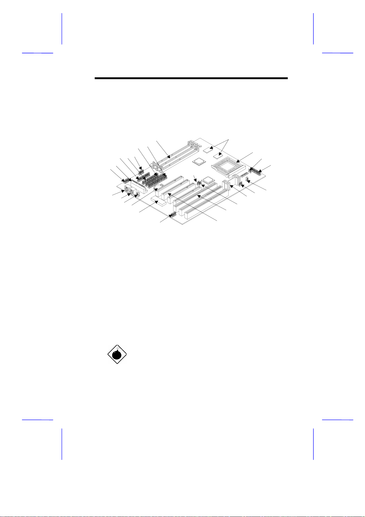
Figure 1-1 shows the board layout and the locations of the important
components.
18
17
9
10
11
12
13
14
15
16
6
3
5
4
2
1
24
23
22
21
1 COM1 connector 14 HDD LED connector
2 Power connector 15 Voltage regulator with heatsink
3 Parallel/Printer connector 16 InfraRed (IrDA) connector
4 Floppy disk drive connector 17 ISA slots
5 COM2 connector 18 PCI slots
6 IDE2 connector 19 USB connector
7 IDE1 connector 20 BIOS chip
8 DIMM sockets 21 Battery
9 Second-level cache 22 Resume Power connector
10 CPU socket 23 PS/2 mouse port
11 Power button connector 24 PS/2 keyboard port
12 Multifunction connector 25 Ring-in connector
13 2-pin fan connector
8
7
25
20
19
Figure 1-1 System Board Layout
The heatsink becomes very hot when the
system is on. NEVER touch the heatsink with
any metal or with your hands.
System Board 1-3

1.4 Jumpers and Connectors
1.4.1 Jumper and Connector Locations
Figure 1-2 shows the jumper and connector locations.
Figure 1-2 Jumper and Connector Locations
The shaded pin indicates pin 1.
1-4 User’s Guide

1.4.2 Jumper Settings
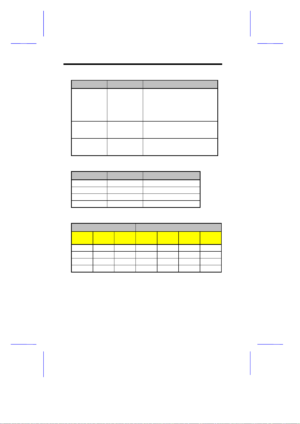
The following tables list the jumper settings and their corresponding
functions:
Table 1-1 Jumper Settings
Jumper Setting Function
Power Supply Type
JP1
1-3, 2-4
3-5, 4-6
JP4 1-2
2-3 *
JP5 1-2
2-3
3-4 *
JP7
1-2
3-4
5-6 *
*
Traditional power supply
Resume power supply
L2 Burst Mode
Linear burst
Interleave / 1+4 mode
BIOS Programming Voltage
12V for MX2 2MB
5V for SST, ATMEL
Normal operation
Hardware Monitoring
Vcore
3.2V
2.9V
2.8V
JP9
1-2
3-4 *
JP10
1-2
2-3 *
JP8 1-3, 2-4
3-5, 4-6
VI/O
3.5V
3.3V
Thermal Event
Disabled
Enabled
CPU Type
Dual-voltage CPU (P55C)
Single-voltage CPU (P54C)
*
Default
System Board 1-5

Table 1-1 Jumper Settings (continued)
)
Jumper Setting Function
CPU Core Voltage
JP11 1-2 *
3-4
5-6
7-8
9-10
S2 of SW1 On
Off
S3 of SW1 On
Off
3.3V
2.8V
2.9V
3.2V
3.5V
Boot Logo
OEM
Acer
Password Check
Check password
Bypass password
Table 1-2 Host Bus Frequency Select
JP2 JP3 Host Bus
1-3, 2-4 3-5, 4-6 60 MHz
3-5, 4-6 * 3-5, 4-6 * 66 MHz *
1-3, 2-4 1-3, 2-4 75 MHz
3-5, 4-6 1-3, 2-4 83.3 MHz
Table 1-3 CPU/Host Bus Frequency Ratio
SW1 Switch No. Ratio
S4 S5
(BF1/X34
S6
(BF0/Y33)
Intel M2 6x86L K6
Off Off Off 1.5/3.5 3.5 3 3.5
Off Off On 2 2 2
Off On On 2.5 2.5 2 2.5
OffOnOff3333
1-6 User’s Guide

1.4.3 Onboard Connectors
Table 1-4 lists the onboard connectors.
Table 1-4 Onboard Connectors
Connector Function
CN1 COM1 connector
CN2 COM2 connector
CN3 AT keyboard connector (optional)
CN4 PS/2 keyboard port
CN5 PS/2 mouse port
CN6 Resume power connector
CN7 Main power connector
CN8 Printer/parallel connector
CN9 Floppy disk drive connector
CN10 IDE channel 2 connector
CN11 IDE channel 1 connector
CN12 Connector for clearing CMOS
CN13 WOL (wake-on LAN) connector
CN15 IrDA (InfraRed) connector
CN16 Modem ring-in connector
CN17 USB (Universal Serial Bus) connector
CN18 Power button connector
CN19 Multifunction connector
CN20 HDD LED connector
CN21 CPU fan connector
CN22 CPU fan and H/W monitoring connector
System Board 1-7

1.4.4 Front Panel Connectors
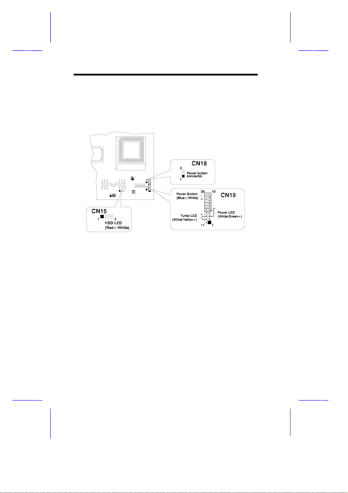
The following figure shows the pin orientation of the front panel
connectors available on board:
Figure 1-3 Front Panel Connectors
1-8 User’s Guide
 Loading...