ZILOG Z8C520PSC, Z8C520SSC, Z8E520PSC, Z8E520SSC Datasheet

DS97KEY2005
P R E L I M I N A R Y
1
P
RELIMINARY
P
RODUCT
S
PECIFICATION
Z8E520/C520
1
1.5 MBPS USB L
OW
-P
OWER
D
EVICE
C
ONTROLLER
F
OR
M
ULTIPROTOCOL
P
OINTING
D
EVICES
FEATURES
■
Six Vectored Interrupts with Fixed Priority
■
Processor Speed Dividable by Firmware Control
■
Operating Current: 5 mA typical in USB Mode; 2.5 mA
typical in Serial Mode (@ 3 MHz); 5 mA typical in PS/2
Mode
■
16 Total Input/Output Pins (Open-Drain/Push-Pull)
Configurable
■
6 inputs with 3 level Programmable Reference
Comparators
■
16-Bit Programmable Watch-Dog Timer (WDT) with
Internal RC Oscillator
■
Software Programmable Timers Configurable as:
– Two 8-Bit Standard Timers and One 16-Bit
Standard Timer or
– One 16-Bit Standard Timer and One 16-Bit Pulse
Width Modulator (PWM) Timer
■
Identical Masked ROM Version (Z8C520)
■
On-Chip Oscillator that accepts a Ceramic Resonator or
External Clock
■
Hardware Support for PS/2, Serial, USB, and GeneralPurpose I/O (GPIO)
■
Power Reduction Modes:
– STOP Mode (functionality shut down e xcept SMR)
– HALT Mode (XTAL still running-peripherals active)
■
USB SIE Compliant with USB Spec 1.0
■
4.0 VDC to 6.0 VDC Operating Range @ 0 ° C to +70 ° C
GENERAL DESCRIPTION
Zilog’s Z8E520 (OTP) and Z8C520 (Masked ROM) microcontrollers are low-power Z8
Plus
MCUs, designed for the
cost-effective implementation of USB and multiprotocol
pointing devices.
For applications demanding powerful I/O capabilities, the
Z8E520's input and output lines are grouped into two ports,
and are configurable under software control to provide timing, status signals, or parallel I/O.
Both 8-bit and 16-bit timers, with a large number of user selectable modes, off-load the system of administering realtime tasks such as counting/timing and I/O data communications.
The microcontroller clock frequency is derived from the
system clock by a programmable divider under firmware
control.
The device is capable of functioning in four distinct, selectable communications modes: PS/2, RS232, GPIO (General-purpose I/O), and USB. The communications mode determines the functionality of the two special serial
communications pins (PB6 and PB7). The device is placed
in the required mode when firmware sets the specified
mode bit in the communications control register. The firmware interface is similar in all modes. The same buffer area
in RAM will accept the data to be transmitted. Up to 8 bytes
may be loaded, and the data will actually be transmitted as
soon as the appropriate command is issued (setting In
Packet Ready in USB mode, for example).
Part ROM RAM Speed
Number (KB) (Bytes) (MHz)
Z8E520 (OTP) 6 176 12
Z8C520 (ROM) 6 176 12
Z8E520/C520
1.5 MBPS USB Device Controller Zilog
2
P R E L I M I N A R Y
DS97KEY2005
GENERAL DESCRIPTION (Continued)
Power connections follow conventional descriptions at
right:
Connection Circuit Device
Power
V
CC
V
DD
Ground GND
V
SS
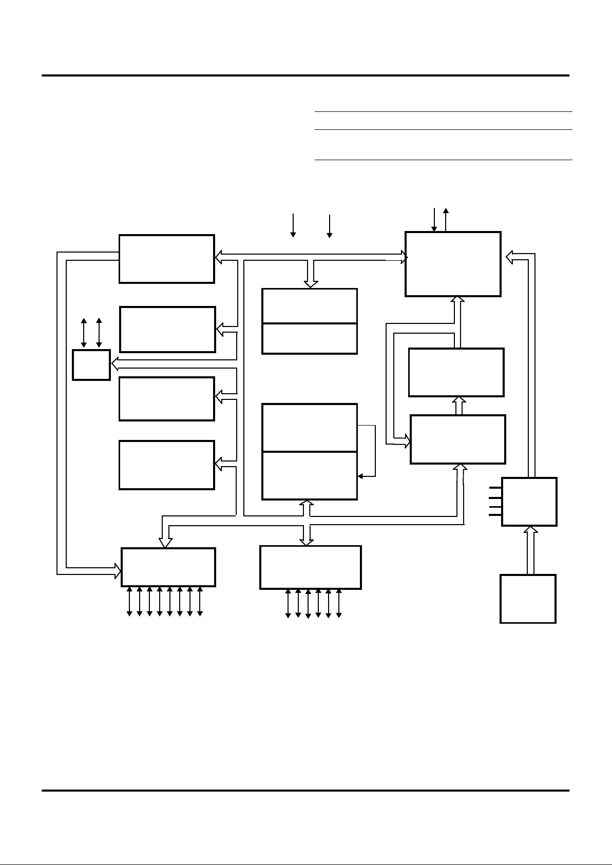
Figure 1. Z8E520 Functional Block Diagram
One 16-bit
Std. Timer
Interrupt
Control
6 Analog
Comparators
ALU
FLAG
Register
Pointer
RAM
Register File
(160 Bytes)
Machine Timing
& Inst. Control
6 K Bytes
Prg. Memory
Program
Counter
V
CC
GND
Ceramic Resonator
Port A
Port B
I/O
Two 8-bit Timers
or
One 16-bit PWM
Timer
I/O
ZIE
WDT
RC OSC
INTERNAL
Port B
(6–7)
Z8E520/C520
Zilog 1.5 MBPS USB Device Controller
DS97KEY2005
P R E L I M I N A R Y
3
1
COMMUNICATION MODES
The Z8E520/C520 allows its user to function in a variety of
communication modes. Having this freedom within a single chip opens up many possibilities when utilizing multiple
protocol applications. The modes incorporated into the
Z8E520/C520 include PS/2, RS232, GPIO, and USB. A
description of each mode is detailed below.
PS/2 Mode . The serial baud rate is fixed at 12.5 K baud.
Received data is automatically checked for parity and
framing errors while HOST abort is supported. The serial
communications pins function as PS/2 compatible DATA
(PB6) and CLOCK (PB7).
RS232 Mode. The data rate is fixed at 1200 baud. The se-
rial communications pins function as RxD (PB6) and TxD
(PB7).
GPIO Mode . In General-Purpose I/O Mode, the serial
communications pins function as standard I/O pins, with
Input, Output P/P (Push/Pull) and OD (Open Drain) Output.
USB Mode . The Z8E520 includes two bidirectional end-
points that support communications compliant to the USB
Specification version 1.0. The serial communications pins
function as D– (PB6) and D+ (PB7). The detailed behavior
of the SIE is controllable by the firmware, and three separate power states are provided for USB Suspend Mode
support (see section below).
USB SUSPEND/RESUME FUNCTIONALITY
Suspend is dedicated through firmware by timing the Activity bit which is set by the SIE.
In Stop Mode, with the WDT disabled, power requirements
are minimized. No power is consumed by the voltage regulator, the Z8
Plus
core, nor differential detector. Only the
Stop Mode Recovery (SMR) is enabled, so an input signal
or Resume from the host can be detected and used to
wake up the microcontroller.
In Stop Mode, with the WDT enabled, slightly more power
is consumed, but the device can wake up periodically to
perform maintenance and detect a change of state in the
application.
USB FUNCTIONAL BLOCK DESCRIPTION
The USB portion of the chip is divided into two areas, the
transceiver and the Serial Interface Engine (SIE). The
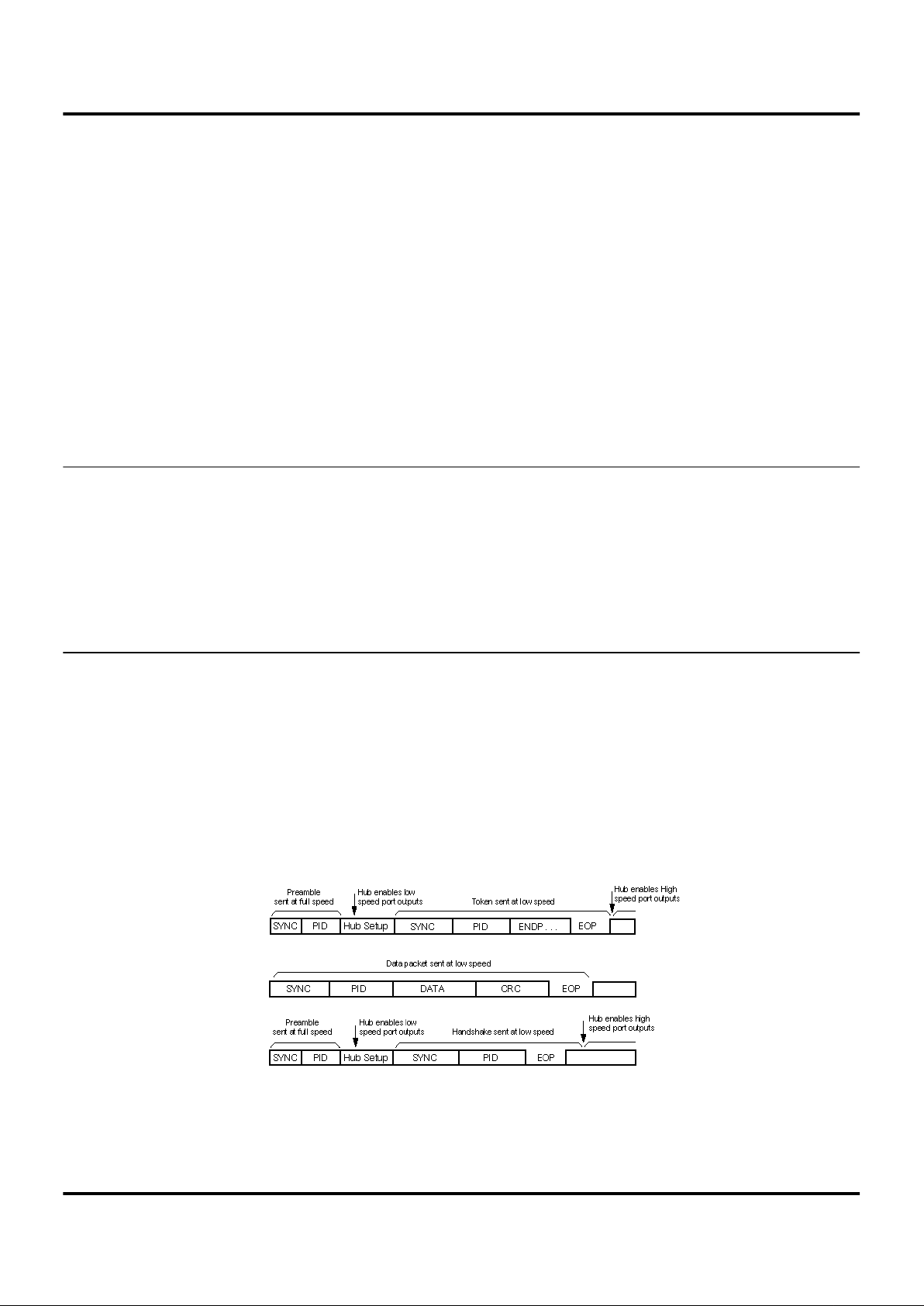
transceiver handles incoming differential signals and “single ended zero (SE0)”. It also converts output data in digital form to differential drive at the proper levels (Figure 2).
The SIE performs all other processing on incoming and out
going data, including signal recovery timing, bit stuffing,
validity checking, data sequencing, and handshaking to
the host. Data flow into and out of the MCU portions are
dedicated registers mapped into Expanded Register File
Memory.
The USB SIE handles three endpoints (control at Endpoint
0, data into the host from Endpoint 1 and data out from the
host as Endpoint 2). All communications are at the
1.5 MB/sec data rate. Endpoint 1 and 2 can be combined
as Control EP1.
Figure 2. Data To/From Z8E520/C520

Z8E520/C520
1.5 MBPS USB Device Controller Zilog
4
P R E L I M I N A R Y
DS97KEY2005
PIN IDENTIFICATION
Figure 3. 20-Pin DIP/SOIC Pin Assignments
PA6
PA7
PB0
PB1
PB2
PB3
PB4
PB5
PA0
PA1
PA5
PA4
XTAL (2)
GND
XTAL (1)
VCC
PB7
PB6
PA3
PA2
20
20-Pin
DIP/SOIC
1
10 11
Table 1. 20-Pin DIP/SOIC Pin Identification
STANDARD Mode
Pin # Symbol Function Direction
1, 2 PA X(6,7) Digital I/O + I SINK Bidirectional
3–8 PB X(0–5) Digital I/O +Comparators Bidirectional
9–12 PA X(0–3) Digital I/O Bidirectional
13–14 PB X (6–7) Digital I/O + Communications Bidirectional
15 V
cc
Power
16 XTAL (1) Clock
17 GND Power
18 XTAL (2) Clock
19, 20 PA X(4,5) Digital I/O + I SINK Bidirectional

Z8E520/C520
Zilog 1.5 MBPS USB Device Controller
DS97KEY2005
P R E L I M I N A R Y
5
1
Figure 4. 20-Pin DIP/SOIC Pin Assignments:
EPROM Programming Mode
D0
D1
D2
D3
D4
D5
D6
D7
TST_CLR
PGM
CLK (1 MHz)
GND
(CLK OUT)
VCC
VPP
ADDRCLK
20
20-Pin
DIP/SOIC
1
10 11
Table 2. 20-Pin DIP/SOIC Pin Identification:
EPROM Programming Mode
EPROM PROGRAMMING Mode
Pin # Symbol Function Direction
1–8 D0–D7 Data Bus I/O
9 TST_CLR Reset Internal Address Counter In
10 PGM Program Pin In
11 ADDRCLK Clock to Address Counter In
12 V
PP
High Voltage to Program Device Power
13–14 Unused
15 V
CC
Power Power
16 CLKOUT Output from Clock Inverter Out
17 GND Power Ref Power
18 CLK 1 MHz to chip In
19 Unused
20 Unused

Z8E520/C520
1.5 MBPS USB Device Controller Zilog
6
P R E L I M I N A R Y
DS97KEY2005
ABSOLUTE MAXIMUM RATINGS
Stresses greater than those listed under Absolute Maximum Ratings may cause permanent damage to the device. This rating is a stress rating only; functional operation
of the device at any condition above those indicated in the
operational sections of these specifications is not implied.
Exposure to absolute maximum rating conditions for an
extended period may affect device reliability. Total power
dissipation should not exceed 880 mW for the package.
Power dissipation is calculated as follows:
Total Power Dissipation = V
DD
x [I
DD
– (sum of I
OH
)]
+ sum of [(V
DD
– V
OH
) x I
OH
]
+ sum of (V
0L
x I
0L
)
Parameter Min Max Units Note
Ambient Temperature under Bias –40 +105 C
Storage Temperature –65 +150 C
Voltage on any Pin with Respect to V
SS
–0.6 +7 V
Voltage on V
DD
Pin with Respect to V
SS
–0.3 +7 V
Total Power Dissipation 880 mW
Maximum Allowable Current out of V
SS
80 mA
Maximum Allowable Current into V
DD
80 mA
Maximum Allowable Current into an Input Pin –600 +600
µ
A 1
Maximum Allowable Current into an Open-Drain Pin –600 +600
µ
A 2
Maximum Allowable Sink Output Current by Any I/O Pin 25 mA
Maximum Allowable Source Output Current by Any I/O Pin 25 mA
Maximum Allowable Sink Output Current by Port A 40 mA
Maximum Allowable Source Output Current by Port A 40 mA
Maximum Allowable Sink Output Current by Port B 40 mA
Maximum Allowable Source Output Current by Port B 40 mA
Notes:
1. Excludes XTAL pins.
2. Device pin is not at an output Low state.
Z8E520/C520
Zilog 1.5 MBPS USB Device Controller
DS97KEY2005
P R E L I M I N A R Y
7
1
STANDARD TEST CONDITIONS
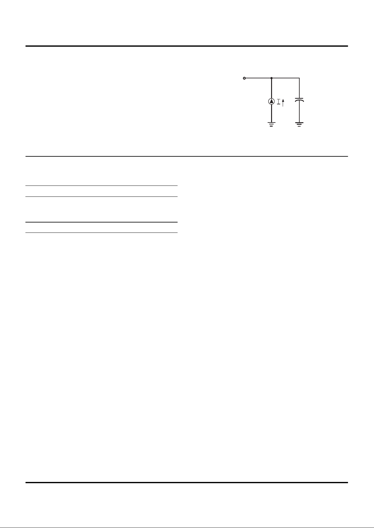
The characteristics listed here apply for standard test conditions as noted. All voltages are referenced to GND. Positive current flows into the referenced pin (Figure 5).
CAPACITANCE
T
A
= 25 ° C; V
CC
= GND = 0V; f = 1.0 MHz; unmeasured pins returned to GND.
Figure 5. Test Load Diagram
From Output
Under Test
150 pF
Parameter Max
Input Capacitance 12 pF
Output Capacitance 12 pF
I/O Capacitance 12 pF
Note: Frequency tolerance ±10%

Z8E520/C520
1.5 MBPS USB Device Controller Zilog
8 P R E L I M I N A R Y DS97KEY2005
DC CHARACTERISTICS: USB MODE
V
cc
= 4.4V – 5.25V
TA = 0°C to +70°C
Sym Parameter
V
CC
Min Max Units Conditions Notes
V
CH
Clock Input High
Voltage
0.7V
CC
VCC+0.3 V Driven by External
Clock Generator
V
CL
Clock Input Low
Voltage
VSS–0.3 0.2V
CC
V Driven by External
Clock Generator
V
IH
Input High Voltage 0.7V
CC
VCC+0.3 V
V
IL
Input Low Voltage VSS–0.3 0.2V
CC
V
V
OH
Output High Voltage
(Port A, B)
VCC–0.4 V IOH = –2.0 mA
V
OL1
Output Low Voltage
(Port A, B)
0.6 V IOL = +4.0 mA 4
V
OL2
Output Low Voltage
(Port A, B)
1.2 V IOL = +6 mA, 4
V
OFFSET
Comparator Input Offset
Voltage
25.0 mV
I
IL
Input Leakage –1.0 2.0 µA VIN = 0V, V
CC
I
OL
Output Leakage –1.0 2.0 µA VIN = 0V, V
CC
V
ICR
Comparator Input
Common Mode
Voltage Range
VSS–0.3 V
CC
–1.0 V
I
CC
Supply Current 6.0V 5.25 6.0 mA @ 6 MHz (Internal open
drain)
1,2
I
CC1
HALT Mode 6.0V 3.5 mA @ 6 MHz (no CPU; RC/WDT
& Detect; D+/D–; I/O active)
1,2
I
CC2
Stop Current 60 µA
I
CC3
Stop Current w/o RC/WDT 40 µA
D+, D– Differential Signaling D– > D+ D+ > D– mV @ >200 mV Difference 3
Notes:
1. All outputs unloaded, I/O pins floating, and all inputs are at V
CC
or VSS level.
2. CL1 = CL2 = 22 pF
3. Except for SE0 for EOP and Reset (see 7.1.4 of USB Specification)
4. General-Purpose I/O Mode.

Z8E520/C520
Zilog 1.5 MBPS USB Device Controller
DS97KEY2005 P R E L I M I N A R Y 9
1
DC CHARACTERISTICS: PS/2 MODE
V
cc
= 4.5V – 5.5V
TA = 0°C to +70°C
Sym Parameter
V
CC
Min Max Units Conditions Notes
V
CH
Clock Input High
Voltage
0.7V
CC
VCC+0.3 V Driven by External
Clock Generator
V
CL
Clock Input Low
Voltage
VSS–0.3 0.2V
CC
V Driven by External
Clock Generator
V
IH
Input High Voltage 0.7V
CC
VCC+0.3 V
V
IL
Input Low Voltage VSS–0.3 0.2V
CC
V
V
OH
Output High Voltage VCC–0.4 V IOH = –2.0 mA
V
OL1
Output Low Voltage 0.6 V IOL = +4.0 mA
V
OL2
Output Low Voltage 1.2 V IOL = +6 mA,
V
OFFSET
Comparator Input Offset
Voltage
25.0 mV
I
IL
Input Leakage –1.0 2.0 µA VIN = 0V, V
CC
I
OL
Output Leakage –1.0 2.0 µA VIN = 0V, V
CC
V
ICR
Comparator Input
Common Mode
Voltage Range
VSS–0.3 V
CC
–1.0 V
I
CC
Supply Current 5.5V 6.0 mA @ 6 MHz 1,2
I
CC1
HALT Current 5.5V 3.5 mA @ 6 MHz (no CPU; no SIE) 1,2
I
CC2
Stop Current 60 µA
I
CC3
Stop Current w/o RC/WDT 40 µA
Notes:
1. All outputs unloaded, I/O pins floating, and all inputs are at V
CC
or VSS level.
2. CL1 = CL2 = 22 pF.

Z8E520/C520
1.5 MBPS USB Device Controller Zilog
10 P R E L I M I N A R Y DS97KEY2005
DC CHARACTERISTICS: RS232 MODE
V
cc
= 4.0V – 6.0V
TA = 0°C to +70°C
Sym Parameter
V
CC
Min Max Units Conditions Notes
V
CH
Clock Input High
Voltage
0.7V
CCVCC
+0.3 V Driven by External
Clock Generator
V
CL
Clock Input Low
Voltage
VSS–0.3 0.2V
CC
V Driven by External
Clock Generator
V
IH
Input High Voltage 0.7V
CCVCC
+0.3 V
V
IL
Input Low Voltage VSS–0.3 0.2V
CC
V
V
OH
Output High Voltage VCC–0.4 V IOH = –2.0 mA
V
OL1
Output Low Voltage 0.6 V IOL = +4.0 mA
V
OL2
Output Low Voltage 1.2 V IOL = +6 mA,
V
OFFSET
Comparator Input Offset
Voltage
25.0 mV
I
IL
Input Leakage –1.0 2.0 µA VIN = 0V, V
CC
I
OL
Output Leakage –1.0 2.0 µA VIN = 0V, V
CC
V
ICR
Comparator Input
Common Mode
Voltage Range
VSS–0.3 V
CC
–1.0 V
I
CC
Supply Current 6.0V 4.0 mA @ 3 MHz (6 MHz/2) 1,2
I
CC1
HALT Mode 6.0V 3.5 mA @ 3 MHz 1,2
I
CC2
Stop Current 60 µA
I
CC3
Stop Current w/o
RC/WDT
40 µA
Notes:
1. All outputs unloaded, I/O pins floating, and all inputs are at V
CC
or VSS level.
2. CL1 = CL2 = 22 pF.

Z8E520/C520
Zilog 1.5 MBPS USB Device Controller
DS97KEY2005 P R E L I M I N A R Y 11
1
DC CHARACTERISTICS: I/O MODE
V
cc
= 4.0V – 6.0V
TA = 0°C to +70°C
Sym Parameter
V
CC
Min Max Units Conditions Notes
V
CH
Clock Input High
Voltage
0.7V
CC
VCC+0.3 V Driven by External
Clock Generator
V
CL
Clock Input Low
Voltage
VSS–0.3 0.2V
CC
V Driven by External
Clock Generator
V
IH
Input High Voltage 0.7V
CC
VCC+0.3 V
V
IL
Input Low Voltage VSS–0.3 0.2V
CC
V
V
OH
Output High Voltage VCC–0.4 V IOH = –2.0 mA
V
OL1
Output Low Voltage 0.6 V IOL = +4.0 mA
V
OL2
Output Low Voltage 1.2 V IOL = +6 mA,
V
OFFSET
Comparator Input Offset
Voltage
25.0 mV
I
IL
Input Leakage –1.0 2.0 µA VIN = 0V, V
CC
I
OL
Output Leakage –1.0 2.0 µA VIN = 0V, V
CC
V
ICR
Comparator Input
Common Mode
Voltage Range
VSS–0.3 V
CC
–1.0 V
I
CC
Supply Current 6.0V 6.0 mA @ 6 MHz 1,2
I
CCA
5.5V 6.0 mA @ 5.5V 1,2
I
CCB
4.0 mA @ 6.0V (6 MHz/2)
I
CC1
HALT w/ RC and WDT 60 µA
I
CC2
50 µA
Notes:
1. All outputs unloaded, I/O pins floating, and all inputs are at V
CC
or VSS level.
2. CL1 = CL2 = 22 pF.
Z8E520/C520
1.5 MBPS USB Device Controller Zilog
12 P R E L I M I N A R Y DS97KEY2005
AC ELECTRICAL CHARACTERISTICS
Timing Diagram
Timing Table
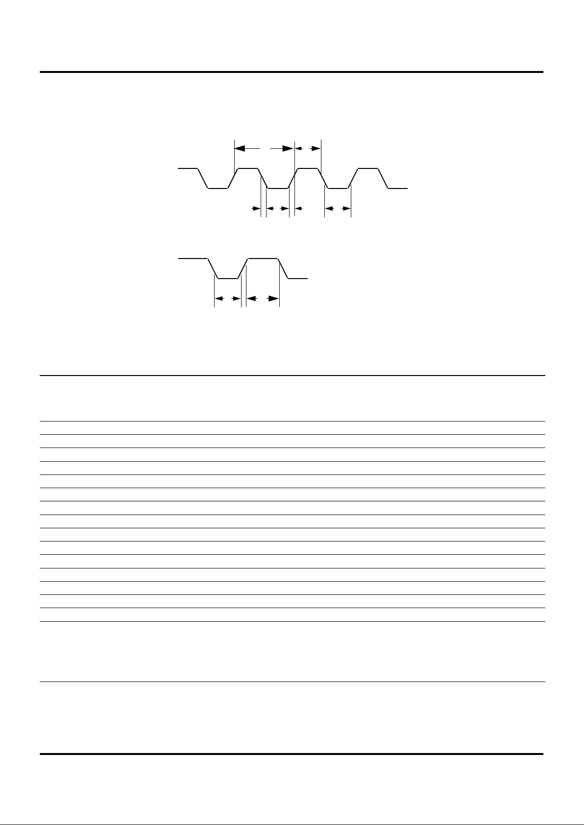
Figure 6. AC Electrical Timing Diagram
1 3
3
2
2
CLOCK
IRQ
N
8
9
TA = 0°C to +70°C
6 MHz
No Symbol Parameter Min Max Units Notes
1 TpC Input Clock Period 83 DC ns 1
2 TrC,TfC Clock Input Rise & Fall Times 5 ns 1
3 TwC Input Clock Width 37 ns 1
4 TwTinL Timer Input Low Width 70 ns 1
5 TwTinH Timer Input High Width 2.5TpC 1
6 TpTin Timer Input Period 4TpC 1
7 TrTin Timer Input Rise & Fall Timer 100 ns 1
8 TwIL Int. Request Low Time 70 ns 1,2
9 TwIH Int. Request Input High Time 3TpC 1,2
10 Twsm Stop-Mode Recovery Width Spec 100TpC ns
11 Tost Oscillator Start-Up Time 0.5 ms
12 Twdt Watch-Dog Timer 1000 ms
13 D+, D– Differential Rise and Fall Times (USB Mode) 70 300 nS 3
14 POR Power supply; POR rate/Volt level
15 TrC RC Clock Period (internal) 12.5 50 µsec 4
Notes:
1. Timing Reference uses 0.7 V
CC
for a logic 1 and 0.2 VCC for a logic 0.
2. Interrupt request
3. See USB Specification 7.1.1.2
4. Corresponds to frequencies of 80 KHz to 20 KHz
Z8E520/C520
Zilog 1.5 MBPS USB Device Controller
DS97KEY2005 P R E L I M I N A R Y 13
1
PIN FUNCTIONS
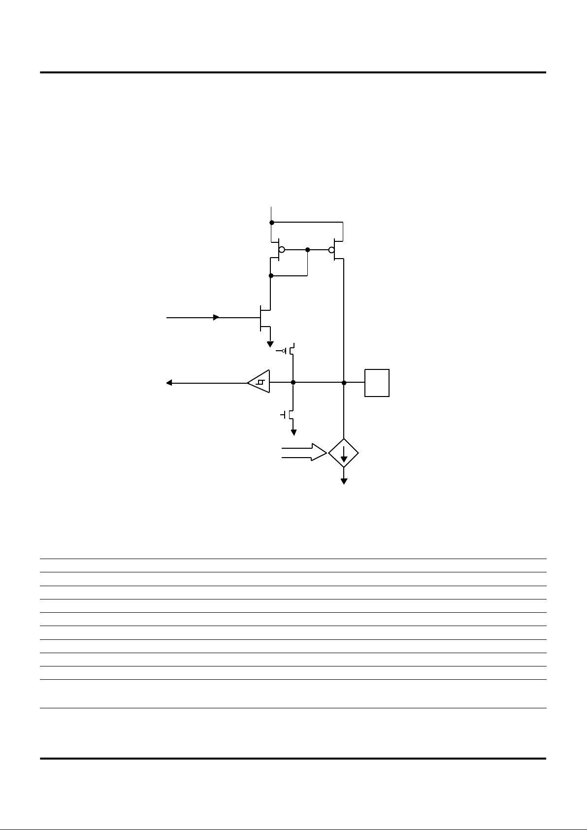
Port A. Port A (4–7) includes a Sink configuration. Port A
(3–0) has a Switch configuration.
In Sink, the options include input wakeup, bidirectional,
push-pull or open drain configurations (Figure 7). The Sink
is programmable from 0–15 mA (in 1 mA increments).
In Switch, the options also include input wakeup, bidirectional, push-pull or open drain configurations (Figure 8).
The only difference between the two is the programmable
Sink option.
Figure 7. Port A (4–7) Sink Configuration
Table 3. Port A (4–7) Programmable Current Sink Table
Symbol Parameter Min. Max. Units Conditions
N Number of Bits Bits 4 bits, 16 settings, 0–15 mA
DNL Diff Non-Linearity 0.50 LSB
I
0
Zero Code/Disable µA Disabled
I
LSB
LSB Current 0.65 1.35 mA 35%
I
F
Full Scale Current 9.75 20.25 mA 35%, Note 1
T
settle
Settling Time 1600 nS Within 10% of final value
I
overshoot
Overshoot Current 1.05*I
set
µA
V
comp
Compliance Voltage 1.1 V Above V
ss
with I
FMAX
Notes:
1. Setting all (4) I
SNK
cells to full scale is a violation of the Absolute Maximum Rating Spec.
0–15 mA/ 1 mA increments
Pad
100K
In
Vcc
Vcc
Wake
TBD
± 30%
I SINK (3:0)
Pullup Resistor Enable
Typical
 Loading...