

Page 1

GENERAL DESCRIPTION
P
RELIMINARY
C
USTOMER PROCUREMENT SPECIFICATION
Z89320
16-BIT DSP DIGITAL
SIGNAL PROCESSOR
The Z89320 is a second generation, 16-bit fractional, two’s
complement CMOS Digital Signal Processor (DSP). Most
instructions, including multiply and accumulate, are
accomplished in a single clock cycle. The processor
contains 1Kbyte of on-chip data RAM (two blocks of 256
16-bit words), 4K words of program ROM. Also, the
processor features a 24-bit ALU, a 16x16 multiplier, a 24bit Accumulator and a shifter. Additionally, the processor
contains a six-level stack, three vectored interrupts and
two inputs for conditional program jumps. Each RAM block
contains a set of three pointers which may be incremented
or decremented automatically to affect hardware looping
without software overhead. The data RAMs can be
simultaneously addressed and loaded to the multiplier for
a true single cycle multiply.
The device includes a 16-bit I/O bus for transferring data
or for mapping peripherals into the processor address
space. Additionally, there are two general purpose user
inputs and two user outputs. Operation with slow peripherals
is accompished with a ready input pin.
Development tools for the IBM PC include a relocatable
assembler, a linker loader, and an ANSI-C compiler. Also,
the development tools include a simulator/debugger, a
cross assembler for the TMS320 family assembly code
and a hardware emulator.
Notes:
All Signals with a preceding front slash, "/", are active Low, e.g.:
B//W (WORD is active Low); /B/W (BYTE is active Low, only).
Power connections follow conventional descriptions below:
Connection Circuit Device
Power V
Ground GND V
CC
V
DD
SS
DC-4128-00 (12-2-92)
1
Page 2
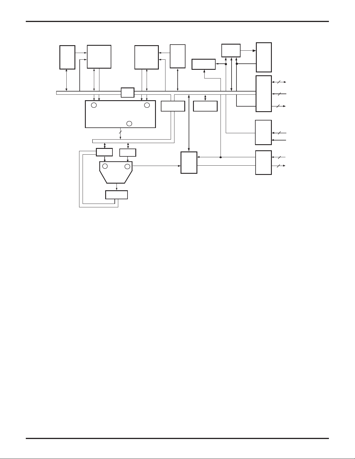
GENERAL DESCRIPTION (Continued)
Register
Pointer
0-2
S-Bus
256 Word
RAM
0
X
16-Bit Bus
16 x16
Multiplier
24-bit
24-Bit Bus
MUX
B A
ALU
ACC
Switch
P
24
Shifter
256 Word
P Bus
RAM
Register
Pointer
Switch
4-6
Status
(5)
Instruction
Register
D Bus
Stack
1
Y
PC
Ready
4K
Word
ROM
16-bit
I/O
Port
Interrupt
User
Port
16
EXT0-15
/RDYE,
ER//W,
/EI
3
EA0-2
3
INTO-2
/RESET
2
UI0-1
2
UO0-1
Functional Block Diagram
2
Page 3
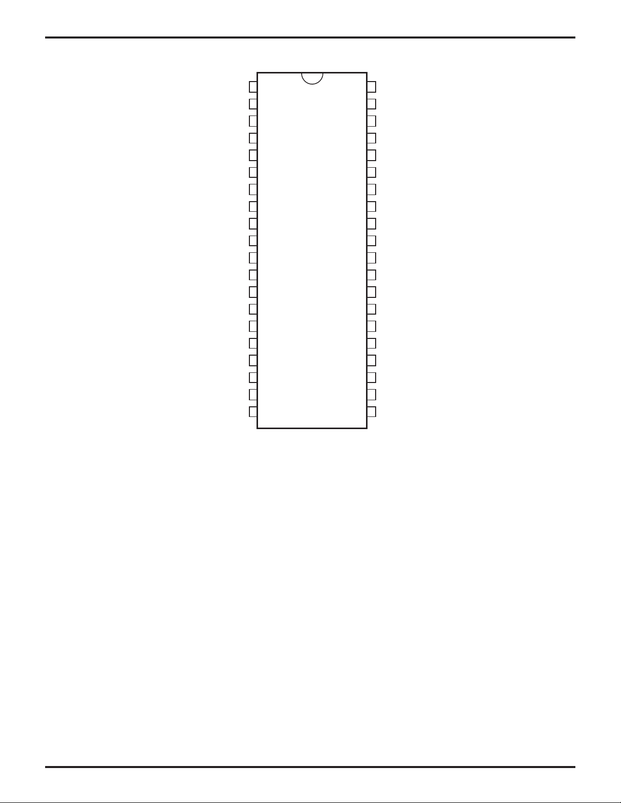
PIN DESCRIPTION
EXT12
EXT13
EXT14
VSS
EXT15
EXT3
EXT4
VSS
EXT5
EXT6
EXT7
EXT8
EXT9
VSS
EXT10
EXT11
INT2
INT1
UI1
UI0
1
2
3
4
5
6
7
8
9
10
11
12
13
14
15
16
17
18
19
20
Z89320
40
39
38
37
36
35
34
33
32
31
30
29
28
27
26
25
24
23
22
21
VSS
EXT2
EXT1
EXT0
VSS
NC (must be VSS)
UO1
UO0
INT0
HALT
CK
/EI
VDD
EA2
EA1
EA0
/RES
/RDYE
ER//W
VDD
40-Pin DIP Pin Assignments
3
Page 4

PIN DESCRIPTION (Continued)
/EI
NC
Uo1
UO0
INT0NCHALT
6543214443424140
CK
VDD
EA2
EA1
VSS
EXT0
EXT1
EXT2
VSS
N/C
EXT12
EXT13
EXT14
VSS
EXT15
7
8
9
10
11
12
13
14
15
16
17
18 19 20 21 22 23 24 25 26 27 28
EXT3
EXT4
44-Pin PLCC Pin Assignments (Standard Mode)
VSS
Z89320
PLCC
EXT5
EXT6
EXT7
NC
EXT8
EXT9
VSS
EXT10
39
38
37
36
35
34
33
32
31
30
29
EA0
/RES
/RDYE
ER//W
VDD
NC
UI0
UI1
INT1
INT2
EXT11
4
Page 5

ABSOLUTE MAXIMUM RATINGS
Storage temperature range -65°C to +150°C
Lead temperature (if packaged) 300°C for 10 sec.
VDD Voltage to V
SS
-0.5 to 7.0V
All other pins VDD+0.5V to VSS-0.5V
STANDARD TEST CONDITIONS
The characteristics listed below apply for standard test
conditions as noted. All voltages are referenced to ground.
Positive current flows into the referenced pin (Test Load
Diagram).
Stresses greater than those listed under Absolute Maximum
Ratings may cause permanent damage to the device. This
is a stress rating only; operation of the device at any
condition above those indicated in the operational sections
of these specifications is not implied. Exposure to absolute
maximum rating conditions for extended period may affect
device reliability.
+5V
2.1 K Ω
From Output
Under Test
150 pF 9.1 K Ω
Test Load Diagram
DC ELECTRICAL CHARACTERISTICS
(V
= 5V ± 5%, TA = 0°C to +70°C unless otherwise specified)
DD
Symbol Parameter Condition Min. Max. Units
I
DD
I
DC
V
IH
V
IL
IL Input Leakage 1 µA
V
OH
V
OL
I
FL
Supply Current VDD=5.25V 40 mA
fclock=10 MHz
DC Power Consumption VDD=5.25V 1 mA 5 mA
Input High Level 0.9 V
DD
Input Low Level 0.1 V
Output High Voltage I
=-100 µAV
OH
-0.2 V
DD
DD
V
V
Output Low Voltage IOL=0.5 mA 0.5 V
Output Floating Leakage Current 5 µA
5
Page 6

AC TIMING DIAGRAM
TCY
PWW
TXVD
CK
TEAD
/EI
ER//W
EXT (15:0)
EA (2:0) Valid Address Out
/RDYE
TIED TIED
EXT Bus:
Output
TXWH
TEAD
Valid
Data Out
TEAD
RDYS
RDYH
WRITE to external device timing
TCY
PWW
CK
/EI
ER//W
EXT (15:0)
EA (2:0) Valid Address Out
/RDYE
TEAD
TIED TIED
EXT Bus:
Input
TXRH
TXRS
Valid
Data In
TEAD
RDYS
RDYH
READ from external device timing
6
Page 7

AC ELECTRICAL CHARACTERISTICS
(V
= 5V ± 5%, TA = 0°C to +70°C unless otherwise specified)
DD
Symbol Parameter Min. Max. Units
TCY Clock Cycle Time 100 1000 ns
PWW Clock Pulse Width 45 ns
Tr Clock Rise Time 2 4 ns
Tf Clock Fall Time 2 4 ns
TEAD EA,ER//W Delay from CK 15 25 ns
TXVD EXT Data Output Valid from CK 5 25 ns
TXWH EXT Data Output Hold from CK 15 ns
TXRS EXT Data Input Setup Time 15 ns
TXRH EXT Data Input Hold from CK 0 15 ns
TIED /EI Delay Time from CK 0 5 ns
RDYS Ready Setup Time 10 ns
RDYH Ready Hold Time 0 ns
Low Margin:
Customer is advised that this product does not meet
Zilog's internal guardbanded test policies for the
specification requested and is supplied on an exception
basis. Customer is cautioned that delivery may be uncertain
and that, in addition to all other limitations on Zilog liability
stated on the front and back of the acknowledgement,
Zilog makes no claim as to quality and reliability under the
CPS. The product remains subject to standard warranty for
replacement due to defects in materials and workmanship.
IBM is a registered trademark of International Business Machines Corporation.
© 1992 by Zilog, Inc. All rights reserved. No part of this document
may be copied or reproduced in any form or by any means
without the prior written consent of Zilog, Inc. The information in
this document is subject to change without notice. Devices sold
by Zilog, Inc. are covered by warranty and patent indemnification
provisions appearing in Zilog, Inc. Terms and Conditions of Sale
only. Zilog, Inc. makes no warranty, express, statutory, implied or
by description, regarding the information set forth herein or
regarding the freedom of the described devices from intellectual
property infringement. Zilog, Inc. makes no warranty of mer-
chantability or fitness for any purpose. Zilog, Inc. shall not be
responsible for any errors that may appear in this document.
Zilog, Inc. makes no commitment to update or keep current the
information contained in this document.
Zilog, Inc. 210 East Hacienda Ave.
Campbell, CA 95008-6600
Telephone (408) 370-8000
FAX 408 370-8056
7
 Loading...