

ZILOG Z89169, Z89165, Z89166, Z89167, Z89168 Datasheet
FEATURES
Z89165/166/167/168/169
DTAD CONTROLLERSZILOG
C
USTOMER
P
ROCUREMENT SPECIFICATION
Z89165/167/169 AND
Z89166/168 (ROMLESS)
ENHANCED DUAL-PROCESSOR
DTAD CONTROLLERS
■ Part Z8 ROM Z8 RAM* Speed
Number (KBytes) (KBytes) (MHz)
Z89165 24 236 20
Z89166 ROMless 236 20
Z89167 24 236 24
Z89168 ROMless 236 24
Z89169 32 236 24
*General-Purpose
■ Part DSP ROM DSP RAM Speed
Number (Words) (Words) (MHz)
Z89165 6K 512 20
Z89166 6K 512 20
Z89167 8K 512 24
Z89168 8K 512 24
Z89169 8K 512 24
■ 68- and 84-Pin PLCC Packages
■ 4.5- to 5.5-Volt Operating Range
■ Low-Power Consumption (200 mW Typical)
■ 0°C to +70°C Temperature Range
■ 25 Expanded Register Files
■ 47 Input/Output Lines (Z89165)
31 Input/Output Lines (Z89166)
43 Input/Output Lines (Core Processor)
■ Six Vectored, Prioritized Z8 Interrupts with
Programmable Polarity
■ Three Vectored, Prioritized DSP Interrupts with
Programmable Polarity
■ Two Analog Comparators
■ Two Programmable Z8 8-Bit Counter/Timers,
Each with Two 6-Bit Programmable Prescaler
■ Watch-Dog Timer /Power-On Reset
■ On-Chip Oscillator that Accepts a Crystal,
Ceramic Resonator, LC, RC, or External Clock Drive
■ RAM and ROM Protect, Low-EMI Option
GENERAL DESCRIPTION
Zilog's Digital Voice Processor Controller family
combines a Z8® microcontroller and a DSP processor
on-chip for a cost-effective turnkey system in digital
telephone answering devices and other voice processing
applications.
The dual-processor architecture is loosely coupled by
mailbox registers and an interrupt system, enabling DSP or
Z8 programs to be directed by events in each other's
domain.
The Z8 microcontroller uses an expanded register file to
allow access to register-mapped peripheral and I/O
circuits for programming versatility.
The 16-bit DSP processor features a 24-bit ALU and
accumulator with single-cycle instructions, providing the
algorithm processing power necessary for telephone voice
quality.
CP96TAD0103
The Z89165/166 devices offer a half-flash 8-bit A/D
converter with up to 128 kHz sample rate and a 10-bit
Pulse-Width modulator (PWM) D/A converter, eliminating
the need for an external CODEC.
The Z89167/168/169 devices feature a hardware ARAM
interface, as well as a dual-CODEC interface. A 10-bit
PWM D/A converter is also on-chip.
Notes:
All Signals with a preceding front slash, "/", are active Low, e.g.:
B//W (WORD is active Low); /B/W (BYTE is active Low, only).
Power connections follow conventional descriptions below:
Connection Circuit Device
Power V
Ground GND V
CC
V
DD
SS
1
ZILOG
GENERAL DESCRIPTION (Continued)
Z89165/166/167/168/169
DTAD CONTROLLERS
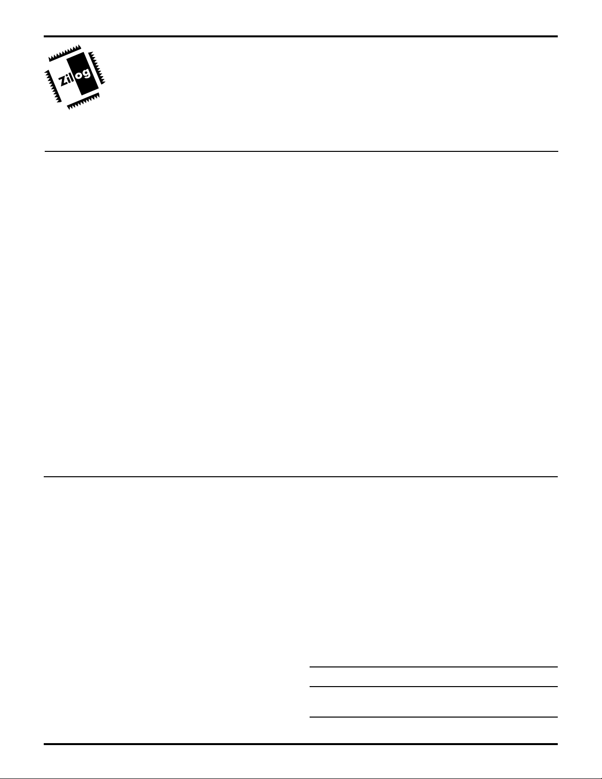
Address
or I/O
(Nibble
Programmable)
Address/Data
or I/O
(Byte
Programmable)
I/O
(Bit
Programmable)
P00
P01
P02
P03
P04
P05
P06
P07
P10
P11
P12
P13
P14
P15
P16
P17
P20
P21
P22
P23
P24
P25
P26
P27
RMLS
/AS
/DS
R/W
XTAL1
XTAL2
VDD
GND
/RESET
Timer 0
Capture Reg.
Port 0
Port 1 Port 4
Register Bus
24 Kbytes
Program
ROM
(Z89165)
Expanded Register
Timer 1
Internal Address Bus
Internal Data Bus
File
(Z8)
Peripheral
Register
(DSP)
mailbox
Port 2 Port 5
6K Words
Program
ROM
Ext.
Memory
Control
OSC
Power
Timer 2 Timer 3
Internal Address Bus
Internal Data Bus
INT 1
INT 2
Register File
256 x 8 Bit
Z8 Core
Expanded
Register Bus
Extended Bus of the DSP
256 Word
RAM 0
Extended Bus of the DSP
256 Word
RAM 1
DSP Core
Port 3
DSP Port
PWM
(10-Bit)
(8-Bit)
ADC
P31
P32
Input
P33
P34
Output
P35
P36
P37
P40
P41
P42
P43
P44
Programmable)
P45
P46
P47
P50
P51
P52
P53
P54
P55
P56
P57
DSP0
DSP1
PWM
AN IN
AN VDD
AN GND
VREF+
VREF-
I/O
(Bit
I/O
(Bit
Programmable)
Z89165/166 Functional Block Diagram
2
CP96TAD0103
GENERAL DESCRIPTION (Continued)
Z89165/166/167/168/169
DTAD CONTROLLERSZILOG
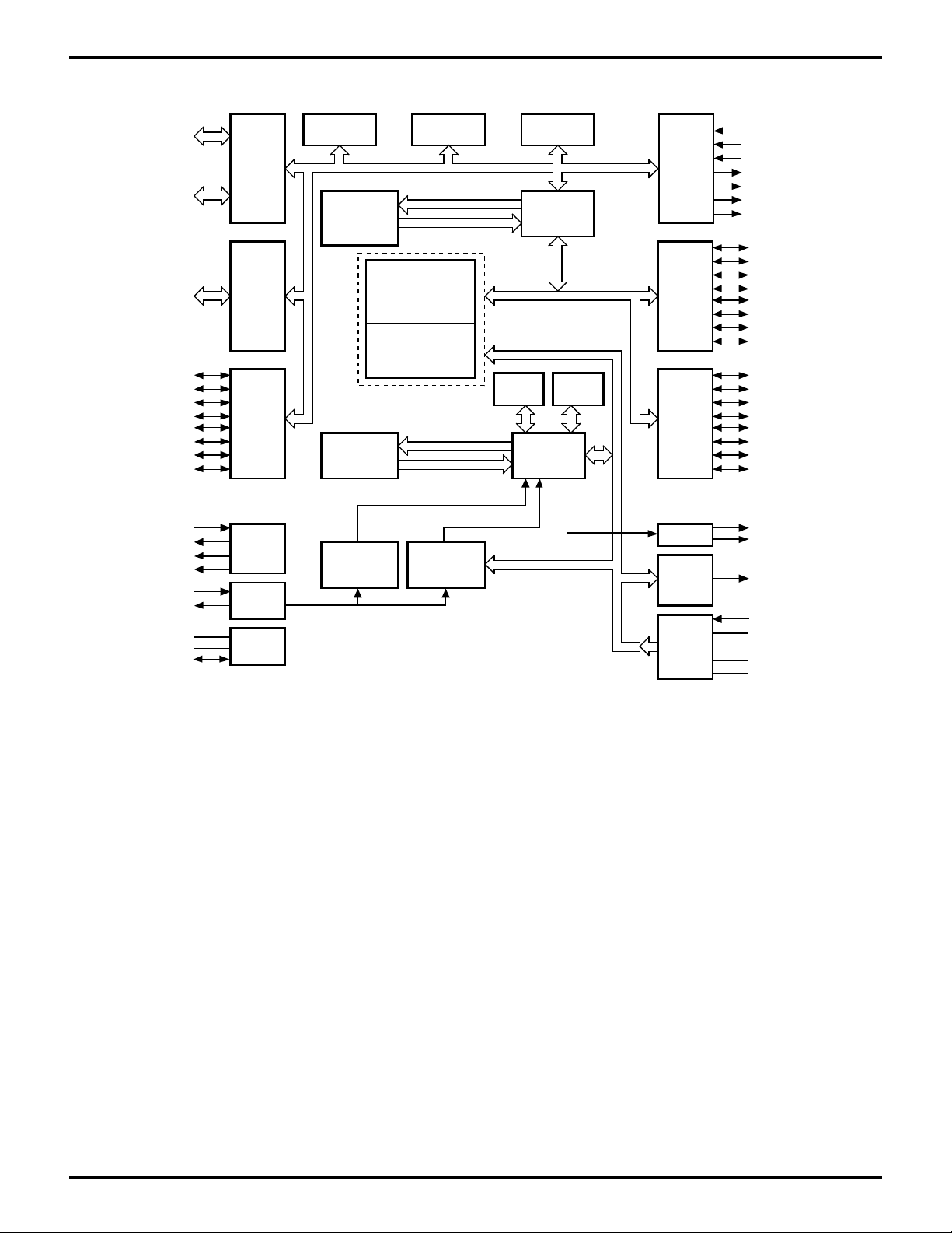
Address
or I/O
(Nibble
Programmable)
Address/Data
or I/O
(Byte
Programmable)
I/O
(Bit
Programmable)
Input
Output
P00
P01
P02
P03
P04
P05
P06
P07
P10
P11
P12
P13
P14
P15
P16
P17
P20
P21
P22
P23
P24
P25
P26
P27
P31
P32
P33
P34
P35
P36
P37
Port 0
Port 1
Port 2
Port 3
Timer0
Z8 Core
Internal Address Bus
Internal Data Bus
8K Words
Program ROM
Peripheral Data Bus of the DSP
Peripheral
Registers
(DSP)
Timer1
Internal Register Bus
24 Kbytes (167)
32 Kbytes (169)
Program ROM
Address Bus
Data Bus
Mailbox
Extended
Register File
(Z8)
Register File
256 x 8-Bit
DSP
Core
Port 4
Port 5
ARAM
Controller
P40
P41
P42
P43
P44
P45
P46
P47
P50
P51
P52
P53
I/O
(Bit
Programmable)
I/O
(Bit
Programmable)
Data0
Data1
Data2
Data3
ADDR0
ADDR1
ADDR2
ADDR3
ADDR4
ADDR5
ADDR6
ADDR7
ADDR8
ADDR9
ADDR10
ARAM_SEL0
ARAM_SEL1
DIN
DENA0
DCLK
DOUT
DENA1
RMLS
/AS
/DS
R/W
PWM
CODEC
Interface
Z8 EXT.
Memory
Control
PWM
(10-Bit)
Timer3 Timer2
Z89167/168/169 Functional Block Diagram
ARAM
Control
Power
-5V
Control
OSC
/RAS
/CAS
ARAM_R/W
ARAM_/OE
/RESET
VDD
GND
Out -5V
XTAL1
XTAL2
CP96TAD0103
3
ZILOG
PIN DESCRIPTION
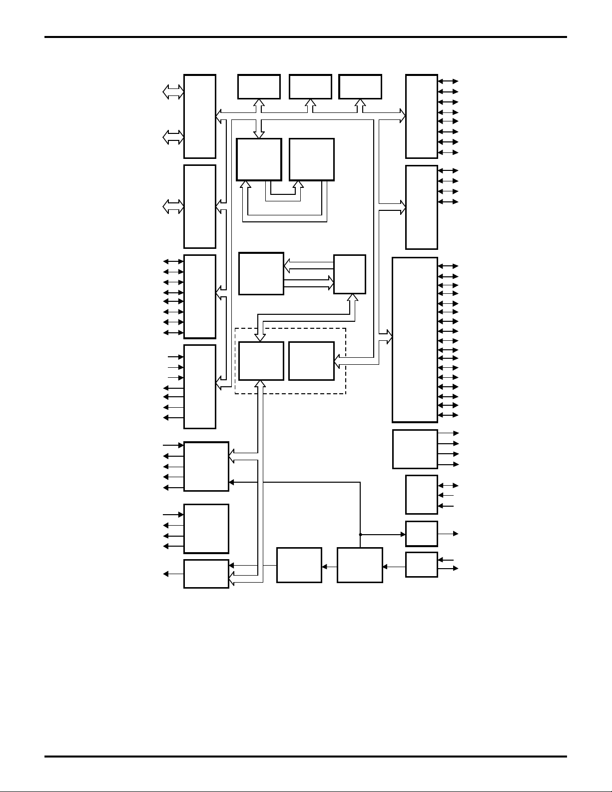
P00
P01
P02
P03
P57
789 654321
P22
P56
P23
P55
P54
GND
P17
P05
P24
P16
P25
P15
P26
P27
N/C
10
11
12
13
14
15
16
17
18
19
20
21
22
23
24
25
26
27 28 29 30 31 32 33 34 35 36 37 38 39 40 41 42 43
P31
P32
P33
P34
VDD
XTAL2
XTAL1
P50
P04
Z89165
P35
P14
VDD
RMLS
/DS
P51
P52
P21
68 67 66 65 64 63 62 61
P36
P13
P37
DSP1
DSP0
P40
P20
P12
P07
P06
GND
P41
ANVDD
60
59
58
57
56
55
54
53
52
51
50
49
48
47
46
45
44
P42
VREF+
ANIN
VREFANGND
/AS
/RESET
R//W
PWM
P10
P47
P11
P46
P53
P45
P44
P43
N/C
XTAL2
XTAL1
P22
P56
P23
P55
P54
GND
P17
P05
P24
P16
P25
P15
P26
P27
SCLK
Z89165/166/167/168/169
P00
P01
P02
P03
P57
P50
P04
VDD
VDD
/DS
P51
P52
P21
P20
789 654321
10
11
12
13
14
15
16
17
18
19
20
21
22
23
24
25
26
27 28 29 30 31 32 33 34 35 36 37 38 39 40 41 42 43
P31
P32
P33
P34
P35
VDD
68 67 66 65 64 63 62 61
Z89166
P14
P36
P13
DSP1
DSP0
P37
P40
P12
DTAD CONTROLLERS
P07
GND
ANVDD
60
VREF+
59
ANIN
58
VREF-
57
ANGND
56
/AS
55
/RESET
54
R//W
53
PWM
52
P10
51
P47
50
P11
49
P46
48
P53
47
P45
46
P44
45
P43
44
/SYNC
P06
P41
P42
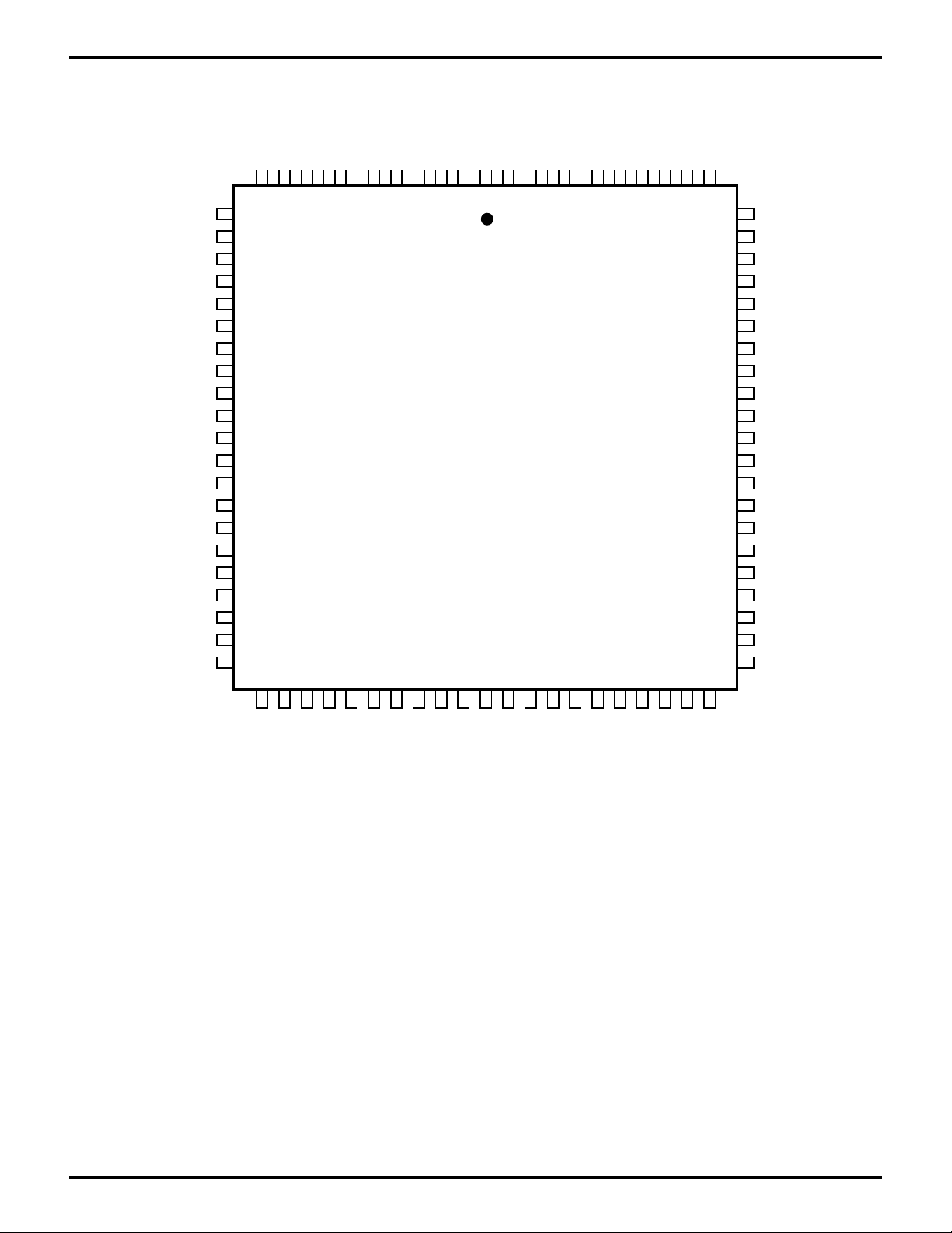
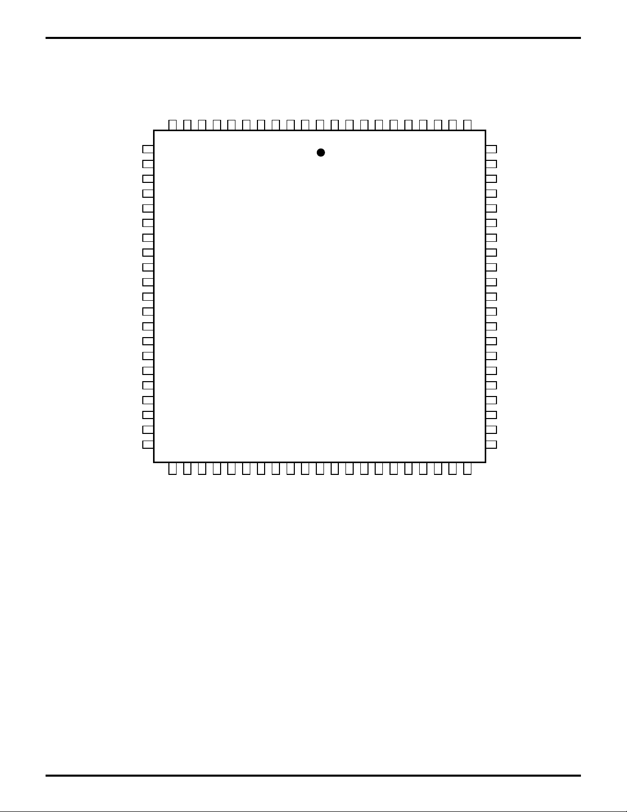
Z89165 68-Pin PLCC Pin Identification Z89166 68-Pin PLCC Pin Identification
Pin Identification
Pin Name Function Direction
+5V Power 5V Power Input
(Digital Power)
GND Power Device Ground
(Digital Ground)
AN AIN 8-Bit A to D Converter Input
Vref– AIN Low Reference Level for
A to D Converter
Vref+ AIN High Reference Level for
A to D Converter
AN VDD Power ADC +5V Power
(Analog Power)
AN GND Power ADC Ground
(Analog Ground)
P00-P07 Data I/O General-Purpose I/O Port
P10-P17 Data I/O General-Purpose I/O Port
P20-P27 Data I/O General-Purpose I/O Port
Pin Name Function Direction
P31-P37 Data I/O General-Purpose I/O Port
P40-P47 Data I/O General-Purpose I/O Port
P50-P57 Data I/O General-Purpose I/O Port
DSP0-DSP1 Data 0 General-Purpose 0 Port
XTAL1 OSC1 20.48 MHz Crystal
Oscillator Input
XTAL2 OSC2 20.48 MHz Crystal
Oscillator Input
/RESET I/O System RESET
PWM Out 10-Bit PWM, 5V TTL Output
4
CP96TAD0103
K
T
PIN DESCRIPTION (Continued)
XTAL1
XTAL2
P27
P26
P25
P24
P23
P22
P21
P20
/DS
P47
P46
P45
P44
P43
P42
P41
P40
C_DIN
C_DOU
Z89165/166/167/168/169
DTAD CONTROLLERSZILOG
ADDR0
ADDR1
ADDR2
ADDR3
ADDR4
ADDR5
ADDR6
ADDR7
ADDR8
ADDR9
ADDR10
ARAM_SEL0
ARAM_SEL1
DATA0
DATA1
DATA2
DATA3
/RAS
/CAS
GND
12
32
11
33
184
Z89168
84-Pin PLCC
42 43
75
74VCC
53
54
VCC
C_CLOC
C_EN0
C_EN1
P50
P51
P52
P53
OUT_5V
GND
/AS
P37
P36
P35
P34
P33
P32
P31
PWM
P10
GND
/RESET
ARAM_OE
ARAM_R/W
P07
P06
P05
P04
P03
P02
P01
P00
VCC
VCC
P17
P16
Z89168 84-Pin PLCC Pin Identification
P15
P14
R/W
P13
P12
P11
CP96TAD0103
5

ZILOG
PIN DESCRIPTION (Continued)
Z89168 84-Pin PLCC Pin Identification
I/O Port
Functions Pin Number I/O Function
Z89165/166/167/168/169
DTAD CONTROLLERS
V
SS
V
CC
32, 54, 65 Digital Ground
12, 44, 74, 45 Digital VCC = +5 V
P00-P07 43-36 Input/Output P00-P07 (General-purpose nibble programmable I/O port.)
P10-P17 55, 53-51, 49-46 Input/Output P10-P17 (General-purpose byte programmable I/O port.)
P20-P27 2-9 Input/Output P20-P27 (General-purpose bit programmable I/O.)
P31-P37 57-63 Input/Output P31-P37 (General-purpose I/O port. Bits P31-P33 are inputs, while
bits P34-P37 are outputs.)
P40-P47 77-84 Input/Output P40-P47 (General-purpose bit programmable I/O.)
P50-P53 70-67 Input/Output P50-P53 (General-purpose bit programmable I/O.)
C_DIN 76 Input Data input from CODEC.
C_DOUT 75 Output Data output to CODEC.
C_CLOCK 73 Output CODEC clock (2.048 MHz)
C_ENA0 72 Output CODEC 0 enable (8 kHz)
C_ENA1 71 Output CODEC 1 enable (8 kHz)
PWM 56 Output Pulse Width Modulator output
DATA0 26 Input/Output Data 0 I/O of the ARAM Interface
DATA1 27 Input/Output Data 1 I/O of the ARAM Interface
DATA2 28 Input/Output Data 2 I/O of the ARAM Interface
DATA3 29 Input/Output Data 3 I/O of the ARAM Interface
ADDR0 13 Output Address 0 line of the ARAM Interface
ADDR1 14 Output Address 1 line of the ARAM Interface
ADDR2 15 Output Address 2 line of the ARAM Interface
ADDR3 16 Output Address 3 line of the ARAM Interface
ADDR4 17 Output Address 4 line of the ARAM Interface
ADDR5 18 Output Address 5 line of the ARAM Interface
ADDR6 19 Output Address 6 line of the ARAM Interface
ADDR7 20 Output Address 7 line of the ARAM Interface
ADDR8 21 Output Address 8 line of the ARAM Interface
ADDR9 22 Output Address 9 line of the ARAM Interface
ADDR10 23 Output Address 10 line of the ARAM Interface for 4 Meg ARAMs. Select 2
output of ARAM Interface for 1 Meg ARAMs support. The latter
mode is used to switch between different pages of ARAM.
ARAM_SEL0 24 Output Select 0 output of ARAM Interface. Used to switch between
different pages of ARAM.
ARAM_SEL1 25 Output Select 1 output of ARAM Interface. Used to switch between
different pages of ARAM.
/RAS 30 Output Row Address Strobe of ARAM Interface.
/CAS 31 Output Column Address Strobe of ARAM Interface.
ARAM_R/W 34 Output Read/Write Strobe of ARAM Interface.
ARAM_/OE 33 Output Output Enable Strobe of ARAM Interface.
XTAL1 11 Input 24.57 MHz crystal input
XTAL2 10 Output 24.57 MHz crystal output
/Reset 35 Input /RESET input
R/W 50 Output Z8® external memory interface R/W output
/AS 64 Output Z8 external memory interface /AS output
/DS 1 Output Z8 external memory interface /DS output
6
CP96TAD0103
K
T
PIN DESCRIPTION (Continued)
XTAL1
XTAL2
P27
P26
P25
P24
P23
P22
P21
P20
/DS
P47
P46
P45
P44
P43
P42
P41
P40
C_DIN
C_DOU
Z89165/166/167/168/169
DTAD CONTROLLERSZILOG
ADDR0
ADDR1
ADDR2
ADDR3
ADDR4
ADDR5
ADDR6
ADDR7
ADDR8
ADDR9
ADDR10
ARAM_SEL0
ARAM_SEL1
DATA0
DATA1
DATA2
DATA3
/RAS
/CAS
GND
12
32
11
33
184
Z89C169/Z89C167
84-Pin PLCC
42 43
75
74VCC
53
54
VCC
C_CLOC
C_EN0
C_EN1
P50
P51
P52
P53
OUT_5V
GND
/AS
P37
P36
P35
P34
P33
P32
P31
PWM
P10
GND
CP96TAD0103
/RESET
ARAM_OE
ARAM_R/W
P07
P06
P05
P04
P03
P02
P01
P00
VCC
P17
RMLS
P16
P15
P14
Z89167/169 84-Pin PLCC Pin Identification
R/W
P13
P12
P11
7
 Loading...