ZILOG Z8913520VSC, Z8913620VSC Datasheet

DS97TAD0300
P R E L I M I N A R Y
1-1
1
P
RELIMINARY
P
RODUCT
S
PECIFICATION
Z89135/Z89136
1
L
OW
-C
OST
DTAD C
ONTROLLER
FEATURES
■
24 KB of Z8 Program ROM (Z89135)
■
Watch-Dog Timer and Power-On Reset
■
Low Power STOP Mode
■
On-Chip Oscillator which Accepts a Crystal or External
Clock Drive
■
Two 8-Bit Z8 Counter Timers with 6-Bit Prescaler
■
Global Power-Down Mode
■
Low Power Consumption - 200 mW (typical)
■
Two Comparators with Programmable Interrupt Priority
■
Six Vectored, Priority Z8 Interrupts
■
RAM and ROM Protect
■
Clock Speed of 20.48 MHz
■
16-Bit Digital Signal Processor (DSP)
■
6K Word DSP Program ROM
■
512 Words On-Chip DSP RAM
■
8-Bit A/D Converter with up to 128 kHz Sample Rate
■
10-Bit PWM D/A Converter (4 kHz to 64 kHz)
■
Three Vectored, Prioritized DSP Interrupts
■
Two DSP Timers to Support Different A/D and
■
D/A Sampling Rates
■
Z8 and DSP Operation in Parallel
■
IBM
®
PC-Based Development Tools
■
Developer’s Toolbox for T.A.M. Applications
IBM is a registered trademark of International Business
Machines Corp.
GENERAL DESCRIPTION
The Z89135/136 is a fully integrated, dual processor controller designed for low-cost digital telephone answering
machines. The I/O control processor is a Z8
®
MCU with 24
KB of program memory, two 8-bit counter/timers, and up to
47 I/O pins. The DSP is a 16-bit processor with a 24-bit
ALU and accumulator, 512 x 16 bits of RAM, single cycle
instructions, and 6K word program ROM plus constants
memory. The chip also contains a half-flash 8-bit A/D converter with up to 128 kHz sample rate and 10-bit PWM D/A
converter. The sampling rates for the converters are programmable. The precision of the 8-bit A/D may be extended by resampling the data at a lower rate in software.
The Z8 and DSP processors are coupled by mailbox registers and an interrupt system, which allows DSP or Z8 programs to be directed by events in each other’s domain.
The Z89136 is the ROMless version of the Z89135. The
DSP is not ROMless. The DSP's program memory is always the internal ROM.
Device
ROM
(KB)
RAM*
(Bytes)
I/O
Lines
Speed
(MHz)
Z89135 24 256 47 20
Z89136 24 256 47 20
Z89135/136 (ROMless)
Low-Cost DTAD Controller Zilog
1-2
P R E L I M I N A R Y
DS97TAD0300
GENERAL DESCRIPTION (Continued)
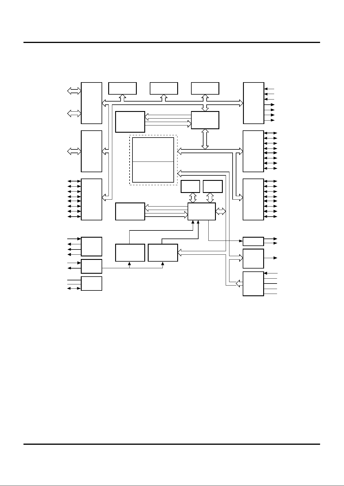
Figure 1. Functional Block Diagram
Port 0
P00
P01
P02
P03
P04
P05
P06
P07
P10
P11
P12
P13
P14
P15
P16
P17
P20
P21
P22
P23
P24
P25
P26
P27
P31
P32
P33
P40
P41
P42
P43
P44
P45
P46
P47
P50
P51
P52
P53
P54
P55
P56
P57
RMLS
/AS
/DS
R/W
Timer 0
Capture Reg.
Port 3
Port 1 Port 4
Port 2 Port 5
Timer 1
Register File
256 x 8 Bit
24 Kbytes
Program
ROM
(Z89165)
Z8 Core
Register Bus
Internal Address Bus
Internal Data Bus
Expanded Register
File
(Z8)
Peripheral
Register
(DSP)
Expanded
Register Bus
Extended Bus of the DSP
6K Words
Program
ROM
DSP Core
Internal Address Bus
Internal Data Bus
DSP Port
PWM
(10-Bit)
ADC
(8-Bit)
Timer 2 Timer 3
Extended Bus of the DSP
Ext.
Memory
Control
OSC
Power
XTAL1
XTAL2
VDD
GND
/RESET
INT 1
INT 2
DSP0
DSP1
AN IN
AN VDD
AN GND
VREF+
VREF-
PWM
256 Word
RAM 0
256 Word
RAM 1
P34
P35
P36
P37
Input
Output
I/O
(Bit
Programmable)
I/O
(Bit
Programmable)
Address
or I/O
(Nibble
Programmable)
Address/Data
or I/O
(Byte
Programmable)
I/O
(Bit
Programmable)
mailbox

Z89135/136 (ROMless)
Zilog Low-Cost DTAD Controller
DS97TAD0300
P R E L I M I N A R Y
1-3
1
Z8 Core Processor
The Z8 is Zilog’s 8-bit MCU core with an Expanded Register File to allow access to register-mapped peripheral and
I/O circuits. The Z8
®
MCU offers a flexible I/O scheme, an
efficient register and address space structure, and a number of ancillary features.
For applications demanding powerful I/O capabilities, the
Z89135/136 offers 47 pins dedicated to input and output.
These lines are grouped into six ports. Each port is configurable under software control to provide timing, status signals and parallel I/O with or without handshake.
There are four basic memory resources for the Z8 that are
available to support a wide range of configurations: Program Memory, Register File, Data Memory, and Expanded
Register File. The Z8 core processor is characterized by
an efficient register file that allows any of 256 on-board
data and control registers to be the source and/or the destination of almost any instruction. Traditional microprocessor accumulator bottlenecks are eliminated.
The Register File is composed of 236 bytes of general-purpose registers, four I/O port register,s and 15 control and
status registers. The Expanded Register File consists of
mailbox registers, WDT mode register, DSP Control register, Stop-Mode Recovery register, Port Configuration register, and the control and data registers for Port 4 and Port
5.
To unburden the software from supporting the real-time
problems, such as counting/timing and data communication, the Z8 offers two on-chip counter/timers with a large
number of user selectable modes.
Watch-Dog Timer and Stop-Mode Recovery features are
software driven by setting specific bits in control registers.
STOP and HALT instructions support reduced power operation. The low power STOP Mode allows parameter information to be stored in the register file if power fails. An
external capacitor or battery retains power to the device.
DSP Coprocessor
The DSP coprocessor is a second generation, 16-bit two’s
complement CMOS Digital Signal Processor (DSP). Most
instructions, including multiply and accumulate, are accomplished in a single clock cycle. The processor contains
two on-chip data RAM blocks of 256 words, a 6K word program ROM, 24-bit ALU, 16 x 16 multiplier, 24-bit Accumulator, shifter, six-level stack, three vectored interrupts, and
two inputs for conditional program jumps. Each RAM block
contains a set of four pointers which may be incremented
or decremented automatically to affect hardware looping
without software overhead. The data RAMs can be simultaneously addressed and loaded to the multiplier for a true
single cycle scalar multiply.
Four external DSP registers are mapped into the expanded register file of the Z8. Communication between the Z8
and the DSP occurs through those common registers
which form the mailbox registers.
The analog signal is generated by a 10-bit resolution Pulse
Width Modulator. The PWM output is a digital signal with
CMOS output levels. The output signal has a resolution of
1 in 1024 with a sampling rate of 16 kHz (XTAL = 20.48
MHz). The sampling rate can be changed under software
control and can be set at 4, 10, 16, and 64 kHz. The dynamic range of the PWM is from 0 to 4V.
An 8-bit resolution half-flash A/D converter is provided.
The conversion is conducted with a sampling frequency of
8, 16, 32, 64, or 128 kHz. (XTAL = 20.48 MHz) in order to
provide oversampling. The input signal is 4V peak to peak.
Scaling is normally ± 1.25V for the 2.5V peak to peak offset.
Two additional timers (Timer2 and Timer3) have been
added to support different sampling rates for the A/D and
D/A converters. These timers are free running counters
that divide the crystal frequency to the appropriate sampling of frequency.
Notes: All signals with a preceding front slash, "/", are ac-
tive Low. For example, B//W (WORD is active Low); /B/W
(BYTE is active Low, only).
Power connections follow conventional descriptions below:
Connection Circuit Device
Power V
CC
V
DD
Ground GND V
SS
Z89135/136 (ROMless)
Low-Cost DTAD Controller Zilog
1-4
P R E L I M I N A R Y
DS97TAD0300
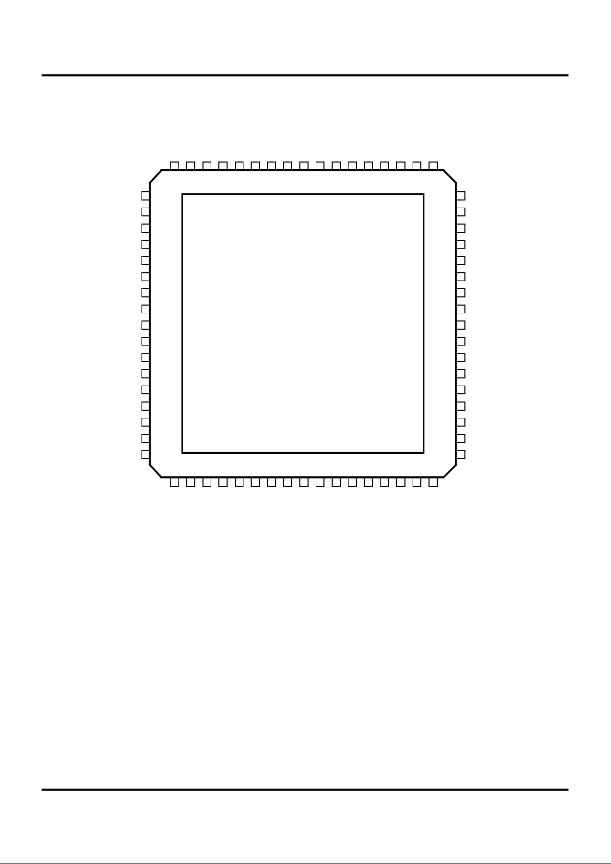
Figure 2. Z89135 68-Pin PLCC Pin Assignments
Z89135
789 654321
10
11
12
13
14
15
16
17
18
19
20
21
22
23
24
25
26
68 67 66 65 64 63 62 61
27 28 29 30 31 32 33 34 35 36 37 38 39 40 41 42 43
60
59
58
57
56
55
54
53
52
51
50
49
48
47
46
45
44
P31
P32
P33
P34
VDD
P35
P14
DSP1
DSP0
P36
P13
P37
P40
P12
P06
P41
P42
VREF+
ANIN
VREFANGND
/AS
/RESET
R//W
PWM
P10
P47
P11
P46
P53
P45
P44
P43
N/C
XTAL2
XTAL1
P22
P56
P23
P55
P54
GND
P17
P05
P24
P16
P25
P15
P26
P27
N/C
P00
P01
P02
P03
P57
P50
P04
VDD
RMLS
/DS
P51
P52
P21
P20
P07
GND
ANVDD
Z89135/136 (ROMless)
Zilog Low-Cost DTAD Controller
DS97TAD0300
P R E L I M I N A R Y
1-5
1
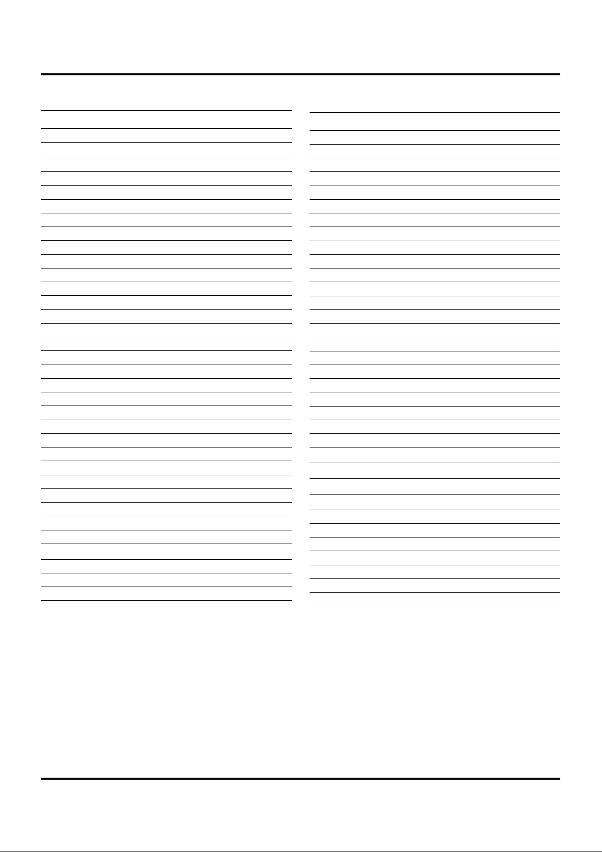
Table 1. Z89135 68-Pin Plastic Leaded Chip Carrier,
Pin Identification
Pin # Symbol Function Direction
1 RMLS ROMless Control Input
2V
DD
Power Supply
3 P04 Port 0, Bit 4 Input/Output
4 P50 Port 5, Bit 0 Input/Output
5 P57 Port 5, Bit 7 Input/Output
6 P03 Port 0, Bit 3 Input/Output
7 P02 Port 0, Bit 2 Input/Output
8 P01 Port 0, Bit 1 Input/Output
9 P00 Port 0, Bit 0 Input/Output
10 XTAL2 Crystal Oscillator Clock Output
11 XTAL1 Crystal Oscillator Clock Input
12 P22 Port 2, Bit 2 Input/Output
13 P56 Port 5, Bit 6 Input/Output
14 P23 Port 2, Bit 3 Input/Output
15 P55 Port 5, Bit 5 Input/Output
16 P54 Port 5, Bit 4 Input/Output
17 GND Ground
18 P17 Port 1, Bit 7 Input/Output
19 P05 Port 0, Bit 5 Input/Output
20 P24 Port 2, Bit 4 Input/Output
21 P16 Port 1, Bit 6 Input/Output
22 P25 Port 2, Bit 5 Input/Output
23 P15 Port 1, Bit 5 Input/Output
24 P26 Port 2, Bit 6 Input/Output
25 P27 Port 2, Bit 7 Input/Output
26 N/C Not Connected
27 P31 Port 3, Bit 1 Input
28 P32 Port 3, Bit 2 Input
29 P33 Port 3, Bit 3 Input
30 P34 Port 3, Bit 4 Output
31 V
DD
Power Supply
32 P35 Port 3, Bit 5 Output
33 P14 Port 1, Bit 4 Input/Output
34 DSP1 DSP User Output 1 Output
35 DSP0 DSP User Output 0 Output
36 P36 Port 3, Bit 7 Output
37 P13 Port 1, Bit 3 Input/Output
38 P37 Port 3, Bit 7 Output
39 P40 Port 4, Bit 0 Input/Output
40 P12 Port 1, Bit 2 Input/Output
41 P06 Port 0, Bit 6 Input/Output
42 P41 Port 4, Bit 1 Input/Output
43 P42 Port 4, Bit 2 Input/Output
44 N/C Not Connected
45 P43 Port 4, Bit 3 Input/Output
46 P44 Port 4, Bit 4 Input/Output
47 P45 Port 4, Bit 5 Input/Output
48 P53 Port 5, Bit 3 Input/Output
49 P46 Port 4, Bit 6 Input/Output
50 P11 Port 1, Bit 1 Input/Output
51 P47 Port 4, Bit 7 Input/Output
52 P10 Port 1, Bit 0 Input/Output
53 PWM Pulse Width Modulator Output
54 R//W Read/Write Output
55 /RESET Reset Input/Output
56 /AS Address Strobe Output
57 ANGND Analog Ground
58 V
REF-
Analog V oltage Ref. Input
59 AN
IN
Analog Input Input
60 V
REF+
Analog V oltage Ref. Input
61 ANV
DD
Analog Power Supply
62 GND Ground
63 P07 Port 0, Bit 7 Input/Output
64 P20 Port 2, Bit 0 Input/Output
65 P21 Port 2, Bit 1 Input/Output
66 P52 Port 5, Bit 2 Input/Output
67 P51 Port 5, Bit 1 Input/Output
68 /DS Data Strobe Output
Table 1. Z89135 68-Pin Plastic Leaded Chip Carrier,
Pin Identification
Pin # Symbol Function Direction
Z89135/136 (ROMless)
Low-Cost DTAD Controller Zilog
1-6
P R E L I M I N A R Y
DS97TAD0300
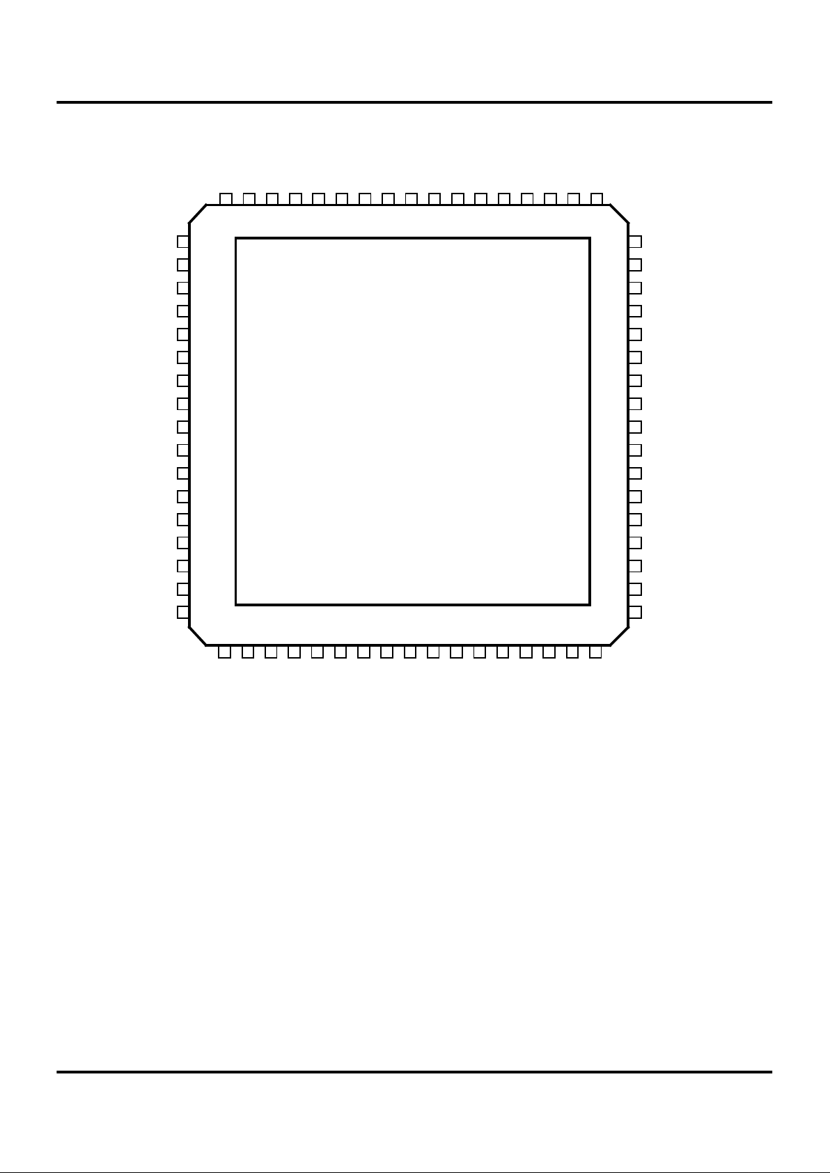
Figure 3. Z89136 68-Pin PLCC Pin Assignments
Z89136
789 654321
10
11
12
13
14
15
16
17
18
19
20
21
22
23
24
25
26
68 67 66 65 64 63 62 61
27 28 29 30 31 32 33 34 35 36 37 38 39 40 41 42 43
60
59
58
57
56
55
54
53
52
51
50
49
48
47
46
45
44
P31
P32
P33
P34
VDD
P35
P14
DSP1
DSP0
P36
P13
P37
P40
P12
P06
P41
P42
VREF+
ANIN
VREFANGND
/AS
/RESET
R//W
PWM
P10
P47
P11
P46
P53
P45
P44
P43
/SYNC
XTAL2
XTAL1
P22
P56
P23
P55
P54
GND
P17
P05
P24
P16
P25
P15
P26
P27
SCLK
P00
P01
P02
P03
P57
P50
P04
VDD
VDD
/DS
P51
P52
P21
P20
P07
GND
ANVDD
Z89135/136 (ROMless)
Zilog Low-Cost DTAD Controller
DS97TAD0300
P R E L I M I N A R Y
1-7
1
Table 2. Z89136 68-Pin Plastic Leaded Chip Carrier,
Pin Identification
Pin # Symbol Function Direction
1V
DD
Power Supply
2V
DD
Power Supply
3 P04 Port 0, Bit 4 Input/Output
4 P50 Port 5, Bit 0 Input/Output
5 P57 Port 5, Bit 7 Input/Output
6 P03 Port 0, Bit 3 Input/Output
7 P02 Port 0, Bit 2 Input/Output
8 P01 Port 0, Bit 1 Input/Output
9 P00 Port 0, Bit 0 Input/Output
10 XTAL2 Crystal Oscillator Clock Output
11 XTAL1 Crystal Oscillator Clock Input
12 P22 Port 2, Bit 2 Input/Output
13 P56 Port 5, Bit 6 Input/Output
14 P23 Port 2, Bit 3 Input/Output
15 P55 Port 5, Bit 5 Input/Output
16 P54 Port 5, Bit 4 Input/Output
17 GND Ground
18 P17 Port 1, Bit 7 Input/Output
19 P05 Port 0, Bit 5 Input/Output
20 P24 Port 2, Bit 4 Input/Output
21 P16 Port 1, Bit 6 Input/Output
22 P25 Port 2, Bit 5 Input/Output
23 P15 Port 1, Bit 5 Input/Output
24 P26 Port 2, Bit 6 Input/Output
25 P27 Port 2, Bit 7 Input/Output
26 SCLK System Clock Output
27 P31 Port 3, Bit 1 Input
28 P32 Port 3, Bit 2 Input
29 P33 Port 3, Bit 3 Input
30 P34 Port 3, Bit 4 Output
31 V
DD
Power Supply
32 P35 Port 3, Bit 5 Output
33 P14 Port 1, Bit 4 Input/Output
34 DSP1 DSP User Output 1 Output
35 DSP0 DSP User Output 0 Output
36 P36 Port 3, Bit 7 Output
37 P13 Port 1, Bit 3 Input/Output
38 P37 Port 3, Bit 7 Output
39 P40 Port 4, Bit 0 Input/Output
40 P12 Port 1, Bit 2 Input/Output
41 P06 Port 0, Bit 6 Input/Output
42 P41 Port 4, Bit 1 Input/Output
43 P42 Port 4, Bit 2 Input/Output
44 /SYNC Synchronization Pin Output
45 P43 Port 4, Bit 3 Input/Output
46 P44 Port 4, Bit 4 Input/Output
47 P45 Port 4, Bit 5 Input/Output
48 P53 Port 5, Bit 3 Input/Output
49 P46 Port 4, Bit 6 Input/Output
50 P11 Port 1, Bit 1 Input/Output
51 P47 Port 4, Bit 7 Input/Output
52 P10 Port 1, Bit 0 Input/Output
53 PWM Pulse Width Modulator Output
54 R//W Read/Write Output
55 /RESET Reset Input/Output
56 /AS Address Strobe Output
57 ANGND Analog Ground
58 V
REF-
Analog V oltage Ref. Input
59 AN
IN
Analog Input Input
60 V
REF+
Analog V oltage Ref. Input
61 ANV
DD
Analog Power Supply
62 GND Ground
63 P07 Port 0, Bit 7 Input/Output
64 P20 Port 2, Bit 0 Input/Output
65 P21 Port 2, Bit 1 Input/Output
66 P52 Port 5, Bit 2 Input/Output
67 P51 Port 5, Bit 1 Input/Output
68 /DS Data Strobe Output
Table 2. Z89136 68-Pin Plastic Leaded Chip Carrier,
Pin Identification
Pin # Symbol Function Direction
Z89135/136 (ROMless)
Low-Cost DTAD Controller Zilog
1-8
P R E L I M I N A R Y
DS97TAD0300
A/D CONVERTER (ADC)
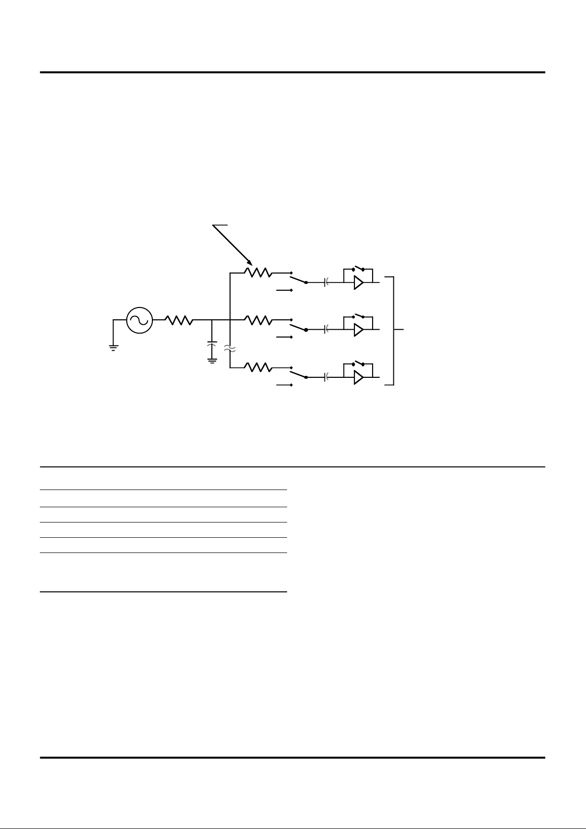
Figure 4 shows the input circuit of the ADC. When conversion starts, the analog input voltage from the input is connected to the MSB and LSB flash converter inputs as
shown in the Input Impedance CKT diagram. Shunting 31
parallel internal resistances of the analog switches and simultaneously charging 31 parallel 1 pF capacitors is equivalent to a 400 Ohms input impedance in parallel with a 31
pF capacitor. Other input stray capacitance adds about 10
pF to the input load. Input source resistances up to 2 Kohms can be used under normal operating conditions without any degradation of the input settling time. For larger input source resistance, longer conversion cycle times may
be required to compensate the input settling time problem.
V
REF
is set using the V
REF
+ pin.
ABSOLUTE MAXIMUM RATINGS
Stresses greater than those listed under Absolute Maximum Ratings may cause permanent damage to the device. This is a stress rating only; operation of the device at
any condition above those indicated in the operational sections of these specifications is not implied. Exposure to absolute maximum rating conditions for an extended period
may affect device reliability.
Figure 4. Input Impedance of ADC
CMOS Switch
on Resistance
2 - 5 k Ω
C Parasitic
R Source
V Ref
C .5 pF
V Ref
C .5 pF
V Ref
C .5 pF
31 CMOS Digital
Comparators
Symbol Description Min Max Units
V
CC
Supply V oltage (*) –0.3 +7.0 V
T
STG
Storage Temp –65 ° +150 ° C
T
A
Oper Ambient Temp † C
Notes:
Voltage on all pins with respect to GND.
† See Ordering Information.
Z89135/136 (ROMless)
Zilog Low-Cost DTAD Controller
DS97TAD0300
P R E L I M I N A R Y
1-9
1
STANDARD TEST CONDITIONS
The characteristics listed below apply for standard test
conditions as noted. All voltages are referenced to GND.
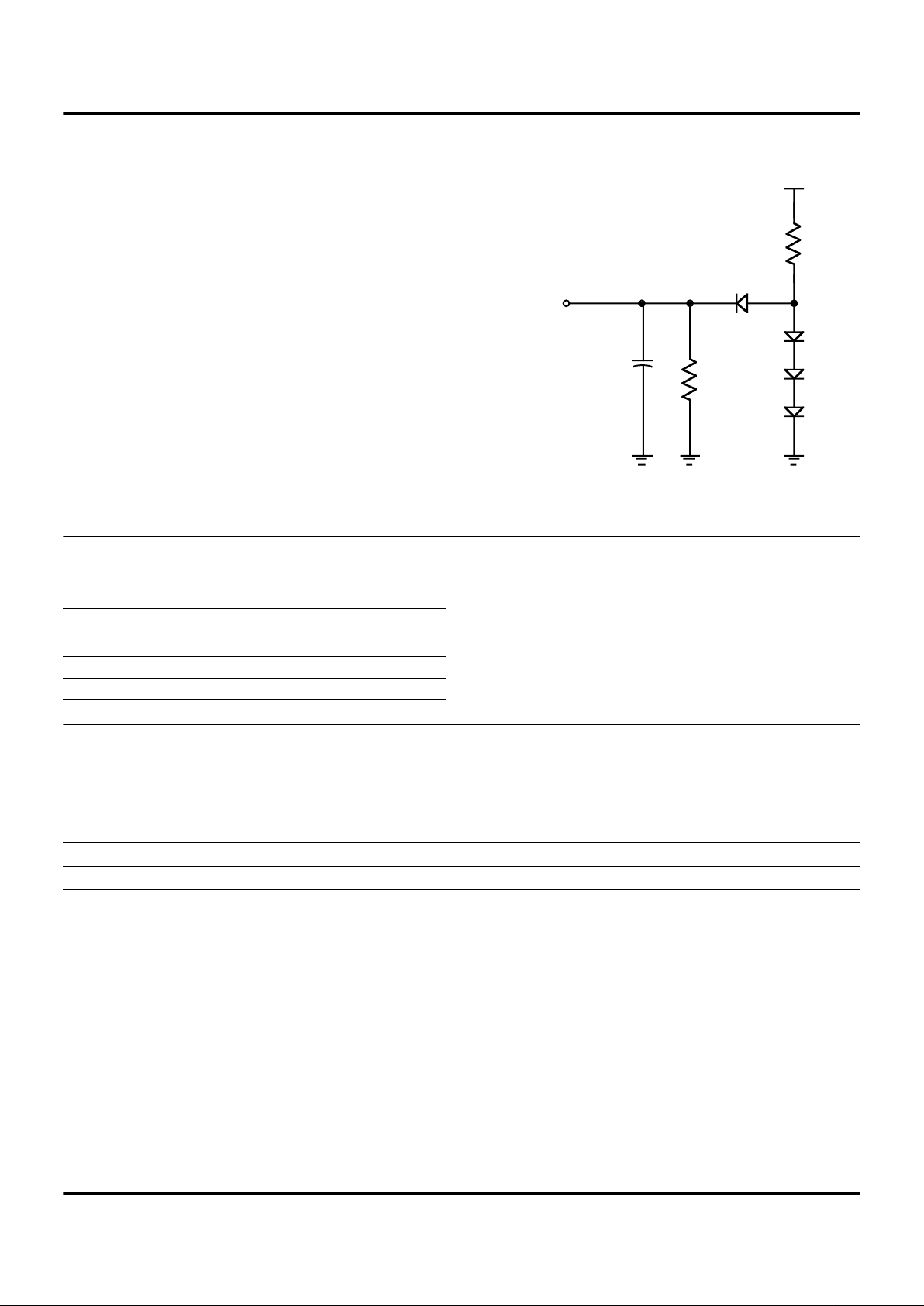
Positive current flows into the referenced pin (Figure 5).
CAPACITANCE
TA = 25°C, VCC = GND = 0V, f = 1.0 MHz, unmeasured pins returned to GND.
DC ELECTRICAL CHARACTERISTICS
Figure 5. Test Load Diagram
+5V
From Output
Under Test
150 pF
9.1 kΩ
2.1 kΩ
Parameter Min Max
Input capacitance 0 12 pF
Output capacitance 0 12 pF
I/O capacitance 0 12 pF
TA = 0°C to +55°C
Typical
Sym Parameter
V
CC
Min Max @ 25°C Units
I
CC
Supply Current 5.0V 65 40 mA
I
CC1
HALT Mode Current 5.0V 20 6 mA
I
CC2
STOP Mode Current 5.0V 400 300 µA
Note: 5.0V ±0.25V.

Z89135/136 (ROMless)
Low-Cost DTAD Controller Zilog
1-10 P R E L I M I N A R Y DS97TAD0300
DC ELECTRICAL CHARACTERISTICS
TA = 0° C to +55°C
Typical
Sym Parameter
V
CC
Min Max @ 25°C Units Conditions
V
MAX
Max Input Voltage 5.0V 7
V
CH
Clock Input High Voltage 5.0V 0.9 V
CC
VCC+0.3 2.5 V Driven by External Clock
Generator
V
CL
Clock Input Low Voltage 5.0V GND–0.3 0.1 V
CC
1.5 V Driven by External Clock
Generator
V
IH
Input High Voltage 5.0V 0.7 V
CC
VCC+0.3 2.5 V
V
IL
Input Low Voltage 5.0V GND–0.3 0.2 V
CC
1.5 V
V
OH
Output High Voltage 5.0V VCC–0.4 4.8 V IOH = –2.0 mA
V
OL1
Output Low Voltage 5.0V 0.4 0.1 V IOL = +4.0 mA
V
OL2
Output Low Voltage 5.0V 1.2 0.3 V IOL = +12 mA, 3 Pin Max
V
RH
Reset Input High Voltage 5.0V 0.8 V
CC
V
CC
2.1 V
V
Rl
Reset Input Low Voltage 5.0V GND–0.3 0.2 V
CC
1.7
V
OFFSET
Comparator Input Offset 5.0V 25 10 mV
Voltage
I
IL
Input Leakage 5.0V –5 5 25 µAVIN = OV, V
CC
I
OL
Output Leakage 5.0V –5 5 25 µAVIN = OV, V
CC
I
IR
Reset Input Current 5.0V –55 –30 µA
Note: 5.0V ±0.25V

Z89135/136 (ROMless)
Zilog Low-Cost DTAD Controller
DS97TAD0300 P R E L I M I N A R Y 1-11
1
DC ELECTRICAL CHARACTERISTICS
Z89165 A/D Converter
TA = 0°C to +55°C
Sym Parameter
V
DD
Min Max Units Conditions
I
IL
Input Leakage Analog Input 5.0V 40 µA ANV
DD
V
IN
V
REFH
V
REFL
=
=
=
=
5.50
0.00
5.50
0.00
V
V
V
V
I
IH
Input Leakage Analog Input 5.25V 2.00 µA ANV
DD
V
IN
V
REFH
V
REFL
=
=
=
=
5.50
5.50
5.50
0.00
V
V
V
V
I
VREFH
Input Current 5.25V 2.00 mA V
IN
V
REFL
ANV
DD
=
=
=
5.50
0.00
5.50
V
V
V
I
V
REFL
Input Current 5.25V 80 µA VIN
V
REFL
ANV
DD
=
=
=
5.50
5.50
5.50
V
V
V
IVEFL
Input Current 5.25V -2.00 mA V
IN
V
REFH
ANV
DD
=
=
=
0.00
5.50
0.00
V
V
V
I
VREFL
Input Current 5.25V -80 µAV
IN
V
REFH
ANV
DD
=
=
=
0.00
5.50
5.50
V
V
V

Z89135/136 (ROMless)
Low-Cost DTAD Controller Zilog
1-12 P R E L I M I N A R Y DS97TAD0300
DC ELECTRICAL CHARACTERISTICS
21 Other Non-Regular I/O
TA = 0°C to +55°C
Sym Parameter
V
DD
Min Max Units Conditions
I
IRH
Input Current ROMless Pin 5.25V 6.00 µAVIN = 5.25 V
I
IR1
Input Current ROMless Pin 5.25V 6.00 µAVIN = 0.00 V
I
IR
Input Current ROMless Pin
During Reset Active
5.25V 1.00 mA VIN = 5.25 V
I
IHX2
Input Current XTAL2 pin in
STOP Mode
5.25V 1.00 µAVIN = 0.00 V
I
ILX2
Input Current XTAL2 Pin in
STOP Mode
5.25V 1.00 µAVIN = 5.25 V
I
IHX1
Input current XTAL1 Pin 5.25V 30 µAVIN = 0.00 V
I
ILX1
Input Current XTAL1 Pin 5.25V 30 µAVIN = 5.25 V
V
OLXR
Output Low Voltage XTAL2
Reset Inactive
5.25V 1.20 V IOL = 4.00 mA
V
OLX
Output Low Voltage XTAL2
Reset Inactive
5.25V 0.60 V IOL = 1.00 mA
V
OHXR
Output High Voltage XTAL2
Reset Inactive
5.25V 4.00 V IOH = 4.00 mA
IV
OHX
Output High Voltage XTAL2
Reset Inactive
5.25V 4.00 V IOH =1.00 mA
I
IH
Input Current P31,P32,P33 5.25V 1.00 µAVIN = 5.25 V
I
IL
Input Current P31, P32, P33 5.25V 1.00 µAVIN = 0.00 V
Z89135/136 (ROMless)
Zilog Low-Cost DTAD Controller
DS97TAD0300 P R E L I M I N A R Y 1-13
1
AC CHARACTERISTIC
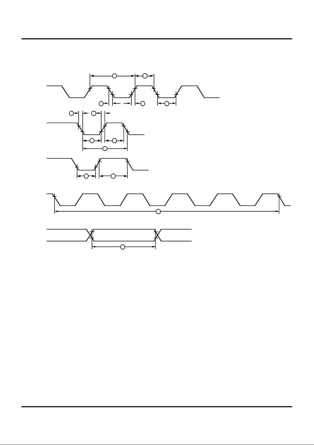
External I/O or Memory Read and Write Timing Diagram
Figure 6. External I/O or Memory Read/Write Timing
R//W
9
12
19
3
16
13
4
5
81811
6
17
10
15714
2
1
Port 0, /DM
Port 1
/AS
/DS
(Read)
Port1
/DS
(Write)
A7 - A0 D7 - D0 IN
D7 - D0 OUTA7 - A0

Z89135/136 (ROMless)
Low-Cost DTAD Controller Zilog
1-14 P R E L I M I N A R Y DS97TAD0300
AC CHARACTERISTICS
External I/O or Memory Read and Write Timing Table
TA=0°C to +55°C
No Symbol Parameter
V
CC
Min Max Units Notes
1 TdA(AS) Address Valid to /AS Rise Delay 5.0V 25 ns 2,3
2 TdAS(A) /AS Rise to Address Float Delay 5.0V 35 ns 2,3
3 TdAS(DR) /AS Rise to Read Data Req’d Valid 5.0V 150 ns 1,2,3
4 TwAS /AS Low Width 5.0V 35 ns 2,3
5 TdAZ(DS) Address Float to /DS Fall 5.0V 0 ns
6 TwDSR /DS (Read) Low Width 5.0V 125 ns 1,2,3
7 TwDSW /DS (Write) Low Width 5.0V 75 ns 1,2,3
8 TdDSR(DR) /DS Fall to Read Data Req’d Valid 5.0V 90 ns 1,2,3
9 ThDR(DS) Read Data to /DS Rise Hold Time 5.0V 0 ns 2,3
10 TdDS(A) /DS Rise to Address Active Delay 5.0V 40 ns 2,3
11 TdDS(AS) /DS Rise to /AS Fall Delay 5.0V 35 ns 2,3
12 TdR/W(AS) R//W Valid to /AS Rise Delay 5.0V 25 ns 2,3
13 TdDS(R/W) /DS Rise to R//W Not Valid 5.0V 35 ns 2,3
14 TdDW(DSW) Write Data Valid to /DS Fall (Write) Delay 5.0V 40 ns 2,3
15 TdDS(DW) /DS Rise to Write Data Not Valid Delay 5.0V 25 ns 2,3
16 TdA(DR) Address Valid to Read Data Req’d Valid 5.0V 180 ns 1,2,3
17 TdAS(DS) /AS Rise to /DS Fall Delay 5.0V 48 ns 2,3
18 TdDI(DS) Data Input Setup to /DS Rise 5.0V 50 ns 1,2,3
19 TdDM(AS) /DM Valid to /AS Fall Delay 5.0V 20 ns 2,3
Notes:
1. When using extended memory timing, add 2 TpC.
2. Timing numbers given are for minimum TpC.
3. See clock cycle dependent characteristics table.
5.0V ±0.25V
Standard Test Load
All timing references use 0.9 V
CC
for a logic 1 and 0.1 VCC for a logic 0.
Z89135/136 (ROMless)
Zilog Low-Cost DTAD Controller
DS97TAD0300 P R E L I M I N A R Y 1-15
1
AC ELECTRICAL CHARACTERISTICS
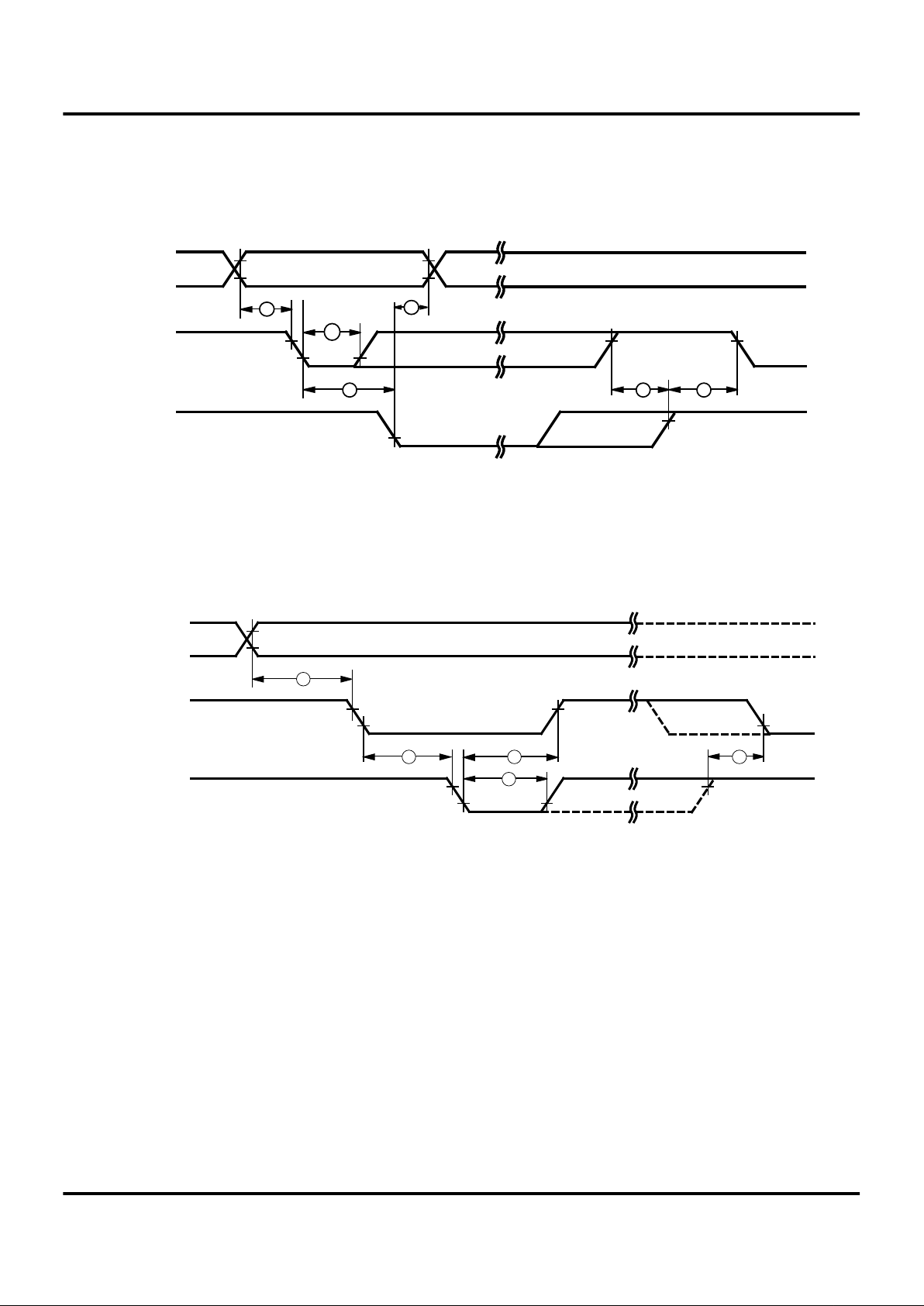
Additional Timing Diagram
Figure 7. Additional Timing
Clock
1
3
4
8
223
TIN
IRQN
6
5
7
7
11
Clock
Setup
10
9
Stop
Mode
Recovery
Source

Z89135/136 (ROMless)
Low-Cost DTAD Controller Zilog
1-16 P R E L I M I N A R Y DS97TAD0300
AC ELECTRICAL CHARACTERISTICS
Additional Timing Table
T
A
=0°C to +55°C
No Symbol Parameter
V
CC
Min Max Units Notes
1 TpC Input Clock Period 5.0V 48.83 ns 1
2 TrC,TfC Clock Input Rise & Fall Times 5.0V 6 ns 1
3 TwC Input Clock Width 5.0V 17 ns 1
4 TwTinL Timer Input Low Width 5.0V 70 ns
5 TwTinH Timer Input High Width 5.0V 3TpC 1
6 TpTin Timer Input Period 5.0V 8TpC 1
7 TrTin,
TfTin
Timer Input Rise & Fall Timer 5.0V 100 ns 1
8A TwIL Int. Request Low Time 5.0V 70 ns 1,2
8B TwIL Int. Request Low Time 5.0V 3TpC 1
9 TwIH Int. Request Input High Time 5.0V 3TpC 1
10 Twsm Stop-Mode Recovery Width
Spec
5.0V 12
5TpC
ns 1
11 Tost Oscillator Start-up Time 5.0V 5TpC 3
12 Twdt Watch-Dog Timer 5.0V
5.0V
5.0V
5.0V
5
15
25
100
ms
ms
ms
ms
D1 = 0, D0 = 0 [4]
D1 = 0, D0 = 1 [4]
D1 = 1, D0 = 0 [4]
D1 = 1, D0 = 1 [4]
Notes:
1. Timing Reference uses 0.9 V
CC
for a logic 1 and 0.1 VCC for a logic 0.
2. Interrupt request through Port 3 (P33-P31)
3. SMR-D5 = 0
4. Reg. WDT
5.0V ±0.25V
Z89135/136 (ROMless)
Zilog Low-Cost DTAD Controller
DS97TAD0300 P R E L I M I N A R Y 1-17
1
AC ELECTRICAL CHARACTERISTICS
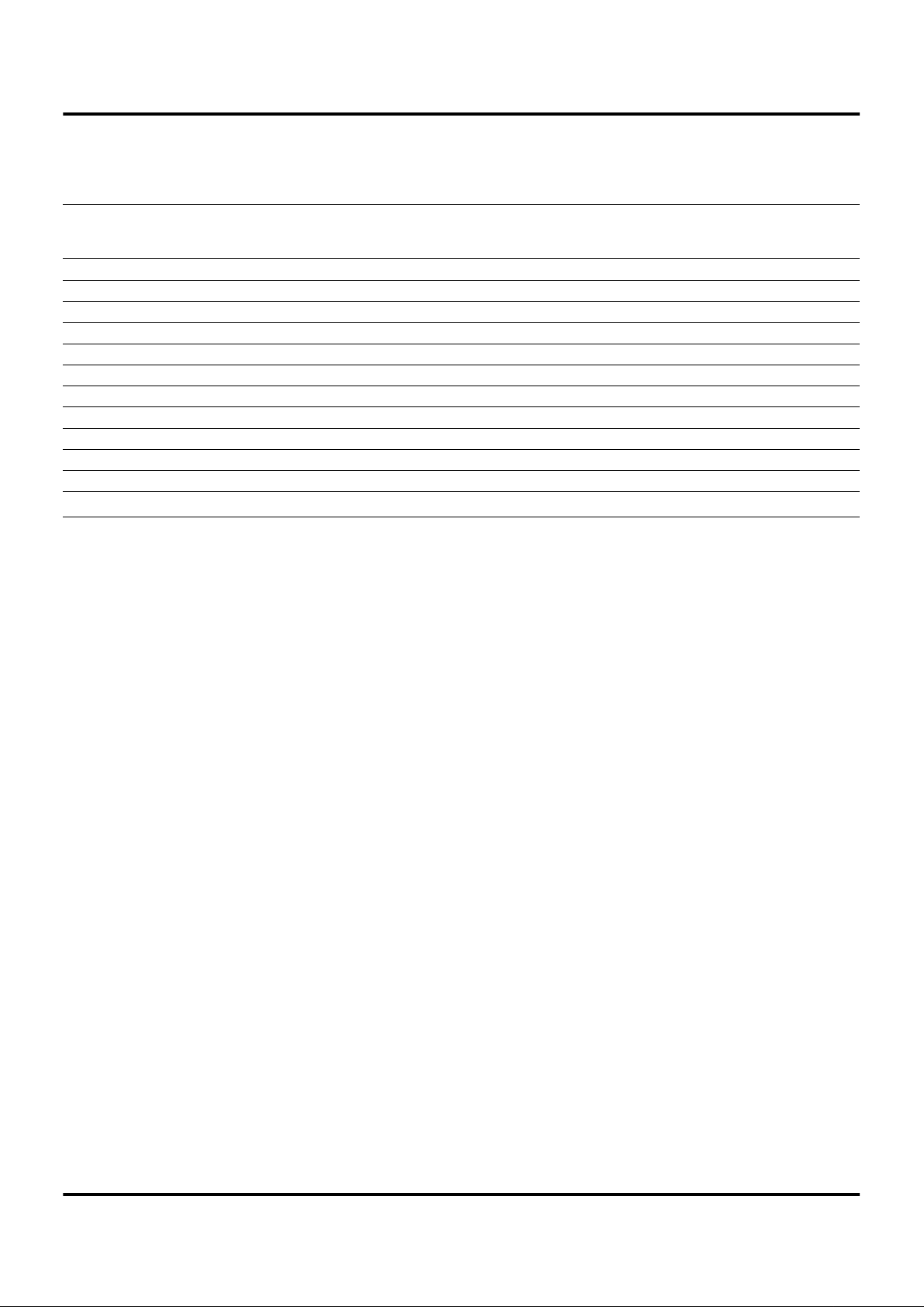
Handshake Timing Diagrams
Figure 8. Input Handshake Timing
Data In
1
3
4
/DAV
(Input)
RDY
(Output)
Next Data In Valid
Delayed RDY
Delayed DAV
Data In Valid
5 6
2
Figure 9. Output Handshake Timing
Data Out
/DAV
(Output)
RDY
(Input)
Next Data Out Valid
Delayed RDY
Delayed DAV
Data Out Valid
7
8 9
10
11
Z89135/136 (ROMless)
Low-Cost DTAD Controller Zilog
1-18 P R E L I M I N A R Y DS97TAD0300
AC ELECTRICAL CHARACTERISTICS (Continued)
Handshake Timing Table
V
CC
TA = 0°C to +55°C
Min Max
Data
DirectionNo Symbol Parameter Units
1 TsDI(DAV) Data In Setup Time 5.0V 0 ns IN
2 ThDI(DAV) RDY to Data Hold Time 5.0V 0 ns IN
3 TwDAV Data Available Width 5.0V 40 ns IN
4 TdDAVI(RDY) DAV Fall to RDY Fall Delay 5.0V 70 ns IN
5 TdDAVId(RDY) DAV Rise to RDY Rise Delay 5.0V 40 ns IN
6 TdDO(DAV) RDY Rise to DAV Fall Delay 5.0V 0 ns IN
7 TcLDAV0(RDY) Data Out to DAV Fall Delay 5.0V TpC ns OUT
8 TcLDAV0(RDY) DAV Fall to RDY Fall Delay 5.0V 0 ns OUT
9 TdRDY0(DAV) RDY Fall to DAV Rise Delay 5.0V 70 ns OUT
10 TwRD Y RD Y Width 5.0V 40 ns OUT
11 TdRDY0d(DAV) RDY Rise to DAV Fall Delay 5.0V 40 ns OUT
Note: 5.0V ±0.25V

Z89135/136 (ROMless)
Zilog Low-Cost DTAD Controller
DS97TAD0300 P R E L I M I N A R Y 1-19
1
AC ELECTRICAL CHARACTERISTICS
A/D Electrical Characteristics
TA = 0°C –55°C; VCC = 5.0V ±0.25V
Parameter Min Max Typical Units
Resolution 8 bits
Integral non-linearity 1 0.5 lsb
Differential non-linearity 0.5 lsb
Zero Error at 25°C50mV
Power Dissipation 75 35 mW
Clock Frequency 20.48 MHz
Clock Pulse Width 35 ns
Analog Input Voltage Range AN
GND
ANV
CC
V
Conversion Time 2 µs
Input Capacitance on 60 pF
VA
HI
range damage AN
GND
ANV
CC
V
VA
LO
range damage AN
GND
ANV
CC
V
AN
GND
V
SS
ANV
CC
V
ANV
CC
AN
GND
V
CC
V

Z89135/136 (ROMless)
Low-Cost DTAD Controller Zilog
1-20 P R E L I M I N A R Y DS97TAD0300
PIN FUCTIONS
/RESET. (input/output, active Low). This pin initializes the
MCU. Reset is accomplished either through Power-On Reset (POR), Watch-Dog Timer reset, Stop-Mode Recovery,
or external reset. During POR and WDT Reset, the internally generated reset is driving the reset pin Low for the
POR time. Any devices driving the reset line must be open
drain to avoid damage from a possible conflict during reset
conditions. A /RESET will reset both the Z8 and the DSP.
For the Z8:
After the POR time, /RESET is a Schmitt-triggered input.
To avoid asynchronous and noisy reset problems, the Z8
is equipped with a reset filter of four external clocks
(4TpC). If the external reset signal is less than 4TpC in duration, no reset occurs. On the fifth clock after the reset is
detected, an internal RST signal is latched and held for an
internal register count of 18 external clocks, or for the duration of the external reset, whichever is longer. Program
execution begins at location 000CH (Hexadecimal), 5-10
TpC cycles after the /RESET is released. The Z8 does not
reset WDT, SMR, P2M, and P3M registers on a StopMode Recovery operation.
For the DSP:
A low level on the /RESET pin generates an internal reset
signal. The /RESET signal must be kept low for at least
one clock cycle. The CPU will fetch a new Program
Counter (PC) value from program memory address
0FFCH after the reset signal is released.
RMLS.
ROMless
(input, active High). This pin, when connected to VDD, disables the internal Z8 ROM. (Note that,
when pulled Low to GND that part functions normally as
the ROM version). The DSP can not be configured as
ROMless. This pin is only available on the Z89135.
R//W.
Read/Write
(output, write Low). The R//W signal defines the signal flow when the Z8 is reading or writing to external program or data memory. The Z8 is reading when
this pin is High and writing when this pin is Low.
/AS.
Address Strobe
(output, active Low). Address Strobe
is pulsed once at the beginning of each machine cycle. Address output is through Port 0/Port 1 for all external programs. Memory address transfers are valid at the trailing
edge of /AS. Under program control, /AS is placed in the
high-impedance state along with Ports 0 and 1, Data
Strobe, and Read/Write.
/DS.
Data Strobe
(output, active Low). Data Strobe is activated once for each external memory transfer. For read
operations, data must be available prior to the trailing edge
of /DS. For write operations, the falling edge of /DS indicates that output data is valid.
XTAL1.
Crystal 1
(time-based input). This pin connects a
parallel-resonant crystal, ceramic resonator, LC, RC network or an external single-phase clock to the on-chip oscillator input.
XTAL2.
Crystal 2
(time-based output). This pin connects a
parallel-resonant, crystal, ceramic resonant, or LC network
to the on-chip oscillator output.
DSP0. (output). DSP0 is a general-purpose output pin
connected to bit 6 of the Analog Control Register (DSP
EXT4). This bit has no special significance and may be
used to output data by writing to bit 6 of the ACR.
DSP1. (output). DSP1 is a general-purpose output pin
connected to bit 7 of the Analog Control Register (DSP
EXT4). This bit has no special significance and may be
used to output data by writing to bit 7 of the ACR.
SCLK.
System Clock
(output). SCLK outputs the system
clock. This pin is available on the Z89136.
/SYNC.
Synchronize
(output). This signal indicates the last
clock cycle of the current executing Z8 instruction. This pin
is only available on the Z89136.
PWM.
Pulse Width Modulator
(output). The PWM is a 10bit resolution D/A converter. This output is a digital signal
with CMOS output levels.
ANIN. (input). Analog input for the A/D converter.
ANVDD. Analog power supply for the A/D converter.
AN
GND
. Analog ground for the A/D converter.
V
REF+
. (input). Reference voltage (High) for the A/D con-
verter.
V
REF
. (input). Reference voltage (Low) for the A/D convert-
er.
VDD. Digital power supply for the Z89135.
GND. Digital ground for the Z89135.
 Loading...