
2
P
RELIMINARY
P
RODUCT
S
PECIFICATION
FEATURES
ROM
Device
Z87010 4 16 44-Pin PLCC
Z87L10 4 16 44-Pin QFP
(Kbyte)
I/O
Lines
Package
Information
44-Pin QFP
Hardware
■
16-Bit DSP Processor
■
3.0V to 3.6V; -20 ° to +70 ° C, Z87L10
4.5V to 5.5V, -20 ° to +70 ° C, Z87010
■
Static Architecture
■
512 Word On-Chip RAM
■
Modified Harvard Architecture
Z87010/Z87L10
A
UDIO
■
■
■
■
■
Software
■
■
■
■
E
NCODER
Direct Interface to 8-Bit µ -law Telephone CODEC
I/O Bus (16-Bit Tristable Data, 3-Bit Address)
Wait State Generator
Two External Interrupts
Four Separate I/O Pins (2 Input, 2 Output)
Full Duplex 32 Kbps ADPCM Encoding/Decoding
Single Tone and DTMF Signal Generation
Sidetone, Volume Control, Mute Functions
Large Phone Number Memory (21 numbers of 23 digits
each)
/D
ECODERS
2
■
Direct Interface to Z87000 Frequency Hopping
Spreader/Despreader
GENERAL DESCRIPTION
The Z87010/Z87L10 is a second generation CMOS Digital
Signal Processor (DSP) that has been ROM-coded by
Zilog to provide full-duplex 32 Kbps, Adaptive Delta Pulse
Code Modulation (ADPCM) speech coding/decoding (CODEC), and interface to the Z87000/Z87L00 Spread Spectrum Cordless Telephone Controller. Together the
Z87000/Z87L00 and Z87010/Z87L10 devices support the
implementation of a 900 MHz frequency-hopping spread
spectrum cordless telephone in conformance with United
States FCC regulations for unlicensed operation.
The Z87010 and Z87L10 are distinct 5V and 3.3V versions
of the ADPCM Audio Encoder/Decoder. For the sake of
brevity, all subsequent references to the Z87010 in this
document also are applicable to the Z87L10, unless specifically noted.
DS96WRL0601
P R E L I M I N A R Y
■
Master-Slave Protocol Interface to Z87000 Spreader/Despreader
The Z87010’s single cycle instruction execution and Harvard bus structure promote efficient algorithm execution.
The processor contains a 4K word program ROM and 512
word data RAM. Six dual operand fetching. Three vectored
interrupts are complemented by a six level stack. The CODEC interface enables high-speed transfer rate to accommodate digital audio and voice data. A dedicated
Counter/Timer provides the necessary timing signals for
the CODEC interface. An additional 13-bit timer is dedicated for general-purpose use.
The Z87010’s circuitry is optimized to accommodate intricate signal processing algorithms and is used here for
speech compression/decompression, generation of DTMF
tones and other cordless telephone functions. Dedicated
hardware allows direct interface to a variety of CODEC
2-1
Z87010/Z87L10
Audio Encoder/Decoders Zilog
GENERAL DESCRIPTION (Continued)
ICs. As configured by the Zilog-provided embedded software for digital cordless phones, the Z87010 supports a
low-cost 8-bit µ -law telephone CODEC. The Z87010 is to
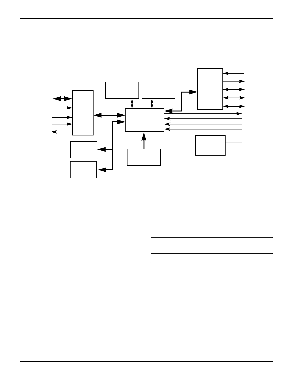
256 Word
RAM0
EXT 0-15
/RDYE
ER//W
16-Bit
I/O
Interface
/EI
EA0-2
Wait
State
Generator
4K Words
Program ROM
13-Bit
Timer
be used with the Z87000 and operates at 16.384 MHz, providing 16 MIPS of processing power needed for the cordless telephone application.
Dual
CODEC
Interface
SCLK
UO0-1
/RESET
DSP
Core
256 Word
RAM1
/INT0-2
Power
VDD
VSS
RXD
TXD
FS0
FS1
UI0-1
Figure 1. Z87010 Functional Block Diagram
Notes: All signals with a preceding front slash, ‘/’, are
active Low, e.g., B//W (WORD is active Low); /B/W (BYTE
is active Low, only).
Power connections follow conventional descriptions below:
Connection Circuit Device
Power V
CC
Ground GND V
V
DD
SS
2-2
P R E L I M I N A R Y
DS96WRL0601
2
Z87010/Z87L10
Zilog Audio Encoder/Decoders
PIN DESCRIPTION
FS1
UO1
UO0
/INTO
FSO
HALT
CLK
/DS
VDD
EA2
EA1
VSS
EXT0
EXT1
EXT2
VSS
RXD
EXT12
EXT13
EXT14
VSS
EXT15
7
17
6
EXT3
VSS
EXT4
1
Z87010
EXT5
EXT6
TXD
EXT7
EXT8
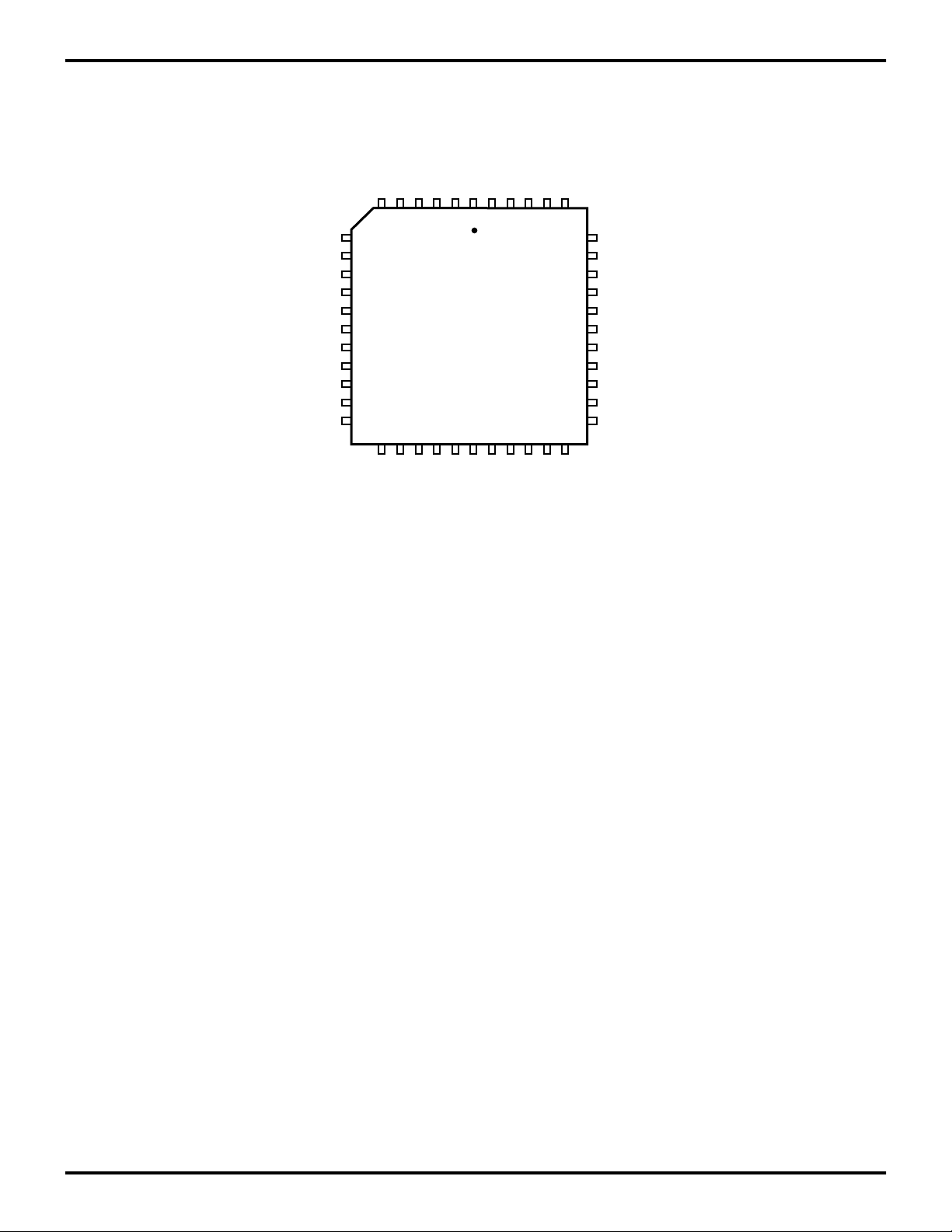
Figure 2. 44-Pin PLCC Pin Assignments
VSS
EXT9
40
39
29
2818
EXT10
EA0
/RESET
WAIT
RD//WR
VDD
SCLK
UI0
UI1
/INT1
/INT2
EXT11
DS96WRL0601
P R E L I M I N A R Y
2-3

Z87010/Z87L10
Audio Encoder/Decoders Zilog
PIN DESCRIPTION (Continued)
Table 1. 44-Pin PLCC Pin Identification
No. Symbol Function Direction
1 HALT Stop execution Input
2 FS0 CODEC0 frame sync Input/Output*
3 /INT0 Interrupt Input
4-5 UO0-UO1 User output Output
6 FS1 CODEC1 frame sync Input/Output*
7,11,16,20,27 V
SS
8-10 EXT0-EXT2 External data bus Input/Output
12 RXD Serial input from CODECs Input
13-15 EXT12-EXT14 External data bus Input/Output
17 EXT15 External data bus Input/Output
18-19 EXT3-EXT4 External data bus Input/Output
21-23 EXT5-EXT7 External data bus Input/Output
24 TXD Serial output to CODECs Output
25-26 EXT8-EXT9 External data bus Input/Output
28-29 EXT10-EXT11 External data bus Input/Output
30 /INT2 Interrupt Input
31 /INT1 Interrupt Input
32 UI1 User input Input
33 UI0 User input Input
34 SCLK CODEC serial clock Input/Output*
35,42 V
DD
36 RD//WR RD /WR strobe for EXT bus Output
37 WAIT WAIT state Input
38 /RESET Reset Input
39-41 EA0-EA2 External address bus Output
43 /DS Data strobe for external bus Output
44 CLK Clock Input
Note: *Defined input or output by interface mode selection
Ground
Power supply Input
2-4
P R E L I M I N A R Y
DS96WRL0601
2
Z87010/Z87L10
Zilog Audio Encoder/Decoders
FS1
UO1
UO0
/INT0
FSO
HALTCK/EI
VDD
EA2
EA1
VSS
EXT0
EXT1
EXT2
VSS
RXD
EXT12
EXT13
EXT14
VSS
EXT15
34
44
1
EXT3
VSS
EXT4
Z87010
EXT5
EXT6
TXD
EXT7
EXT8
EXT9
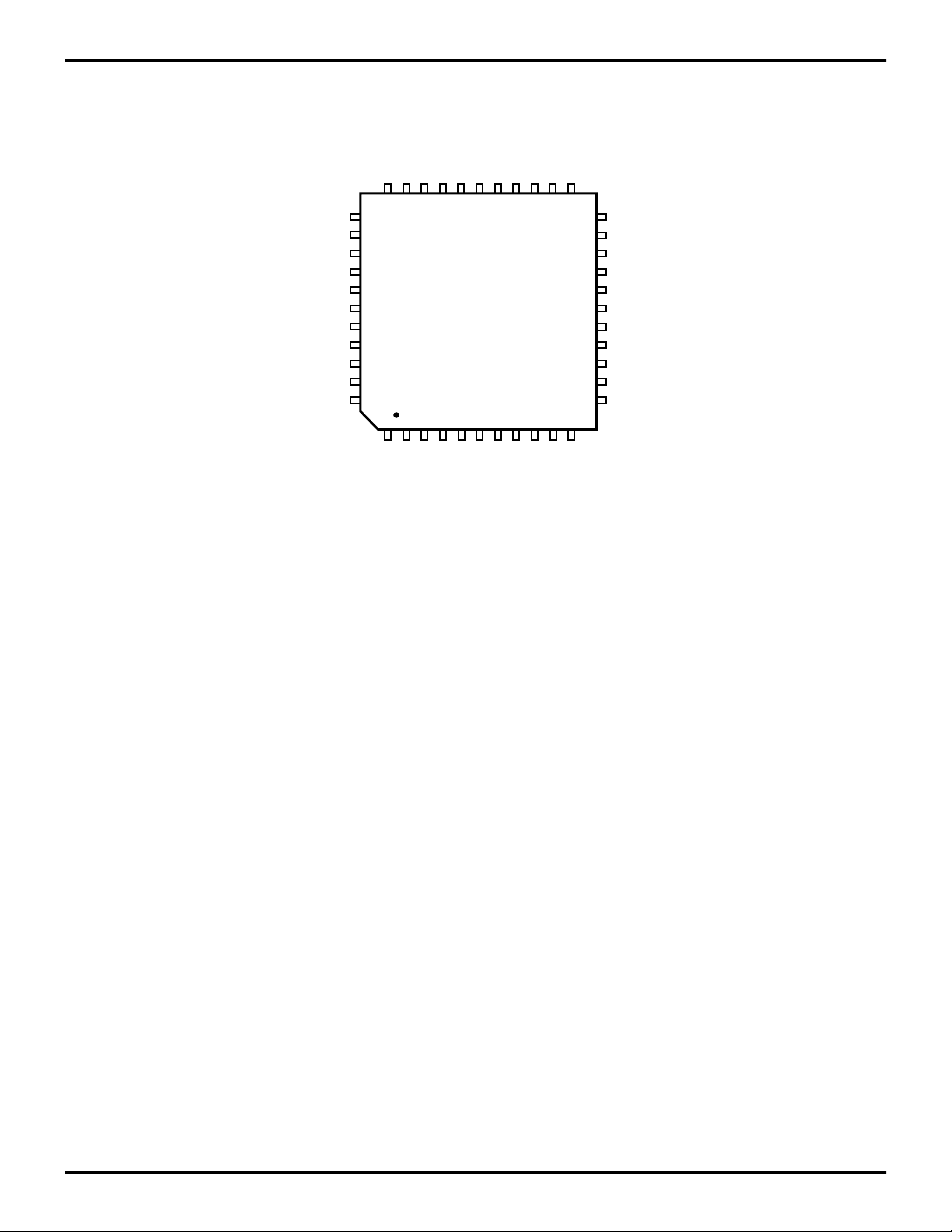
Figure 3. 44-Pin QFP Pin Assignments
2333
12
11
VSS
22
EXT10
EA0
/RES
/RDYE
ER//W
VDD
SCLK
UI0
UI1
/INT1
/INT2
EXT11
DS96WRL0601
P R E L I M I N A R Y
2-5

Z87010/Z87L10
Audio Encoder/Decoders Zilog
PIN DESCRIPTION (Continued)
Table 2. 44-Pin QFP Pin Identification
No. Symbol Function Direction
1-2 EXT3-EXT4 External data bus Input/Output
3,10 V
SS
4-6 EXT5-EXT7 External data bus Input/Output
7 TXD Serial output to CODECs Output
8-9 EXT8-EXT9 External data bus Input/Output
11-12 EXT10-EXT11 External data bus Input/Output
13 /INT2 Interrupt Input
14 /INT1 Interrupt Input
15 UI1 User input Input
16 UI0 User input Input
17 SCLK CODEC serial clock Input/Output*
18,25 V
DD
19 ER//W R/W for External Bus Output
20 /RDYE Data Ready Input
21 /RES Reset Input
22-24 EA0-EA2 External Address Bus Output
26 /EI Data Strobe for External Bus Output
27 CK Clock Input
28 HALT Stop Execution Input
29 FS0 CODEC0 Frame Sync Input/Output*
30 /INT0 Interrupt Input
31-32 U00-U01 User Output –
33 FS1 CODEC1 Frame Sync Input/Output*
34 V
SS
35-37 EXT0-EXT2 External data bus Input/Output
38 V
SS
39 RXD Serial Input to CODEC Input
40-42 EXT12-EXT14 External Data Bus Input/Output
43 V
SS
44 EXT15 External Data Bus Input/Output
Note: *Input or output is defined by interface mode selection.
Ground –
Power supply Input
Ground Input
Ground Input
Ground Input
2-6
P R E L I M I N A R Y
DS96WRL0601
2
≤
≤
Z87010/Z87L10
Zilog Audio Encoder/Decoders
ABSOLUTE MAXIMUM RATING
Symbol Description Min. Max. Units
V
T
Supply V oltage -0.3 +7.0 V
DD
Storage Temp -65 ° C +150 ° CC
STG
T
Oper. Ambient
A
-25 °
+70 °
C
Temp
Note: *Voltage on all pins with respect to GND.
STANDARD TEST CONDITIONS
The characteristics listed below apply for standard test
conditions as noted. All voltages are referenced to ground.
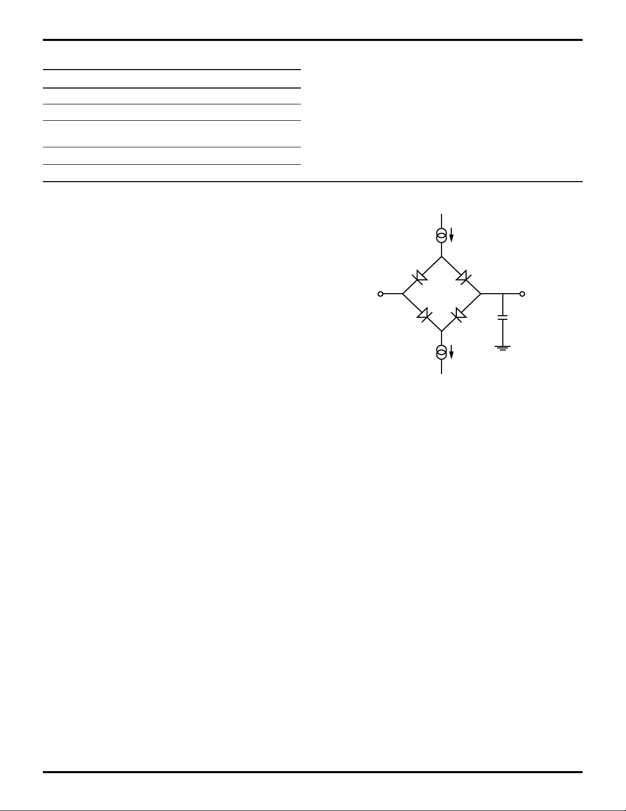
Positive current flows into the referenced pin (Figure 4).
Standard test conditions are as follows:
3.0V ≤ V
4.5V ≤ V
V
= 0V
SS
T
= -20 ° to +70 ° C
A
3.6V (Z87L10)
DD
5.5V (Z87010)
DD
Stresses greater than those listed under Absolute Maximum Ratings may cause permanent damage to the device. This is a stress rating only; operation of the device at
any condition above those indicated in the operational sections of these specifications is not implied. Exposure to absolute maximum rating conditions for extended period may
affect device reliability.
IoL
Threshold
Voltage
IoH
Output
Under
Test
50pF
Figure 4. Test Load Diagram
DS96WRL0601
P R E L I M I N A R Y
2-7
 Loading...