
1
P
RELIMINARY
C
USTOMER
P
ROCUREMENT
S
PECIFICATION
FEATURES
ROM *
Device
Z87001 64 512 32 144-Pin QFP
Z87L01 64 512 32 144-Pin QFP
Note: *Maximum accessible external ROM
Transceiver/Controller Chip Optimized for Implement-
■
ation of 900 MHz Spread Spectrum Cordless Telephone
– Adaptive Frequency Hopping
– Transmit Power Control
– Error Control Signaling
– Handset Power Management
– Support of 32 kbps ADPCM Speech Coding for
(KWords)
High V oice Quality
RAM
(Words)
I/O
Lines
Package
Information
Z87001/Z87L01
ROM
C
■
■
■
■
LESS
ORDLESS
Transceiver Circuitry Provides Primary Cordless Phone
Communications Functions
– Digital Downconversion with Automatic Frequency
– FSK Demodulator
– FSK Modulator
– Symbol Synchronizer
– Time Division Duplex (TDD) Transmit and Receive
On-Chip A/D and D/A to Support 10.7 MHz IF Interface
Up to 64 Kw of External Program Memory Accessible by
the DSP Core
Bus Interface to Z87010 ADPCM Processor
S
PREAD
P
HONE
Control (AFC) Loop
Buffers
S
PECTRUM
C
ONTROLLER
1
■
DSP Core Acts as Phone Controller
– Zilog-Provided Embedded Transceiver Software to
Control Transceiver Operation and Base StationHandset Communications Protocol
– User-Modifiable Software Governs Telephone
Features
GENERAL DESCRIPTION
The Z87001 /Z87L01 FHSS Cordless Telephone Transceiver/Controller is expressly designed to implement a 900
MHz frequency hopping spread spectrum cordless telephone compliant with US FCC regulations for unlicensed
operation. The Z87001 and Z87L01 are distinct 5V and
3.3V versions, respectively, of the core device. For the
sake of brevity, all subsequent references to the Z87001 in
this document also apply to the Z87L01 unless specifically
noted.
The Z87001 is the ROMless version of the Z87000 Spread
Spectrum Controller IC. Specifically intended to facilitate
user specific software development, the Z87001 can access up to 64 kwords of external program ROM.
■
Static CMOS for Low Power Consumption
■
3.0V to 3.6V, -20 ° C to +70 ° C, Z87L01
4.5V to 5.5V, -20 ° C to +70 ° C, Z87001
■
16.384 MHz Base Clock
The Z87001 supports a specific cordless phone system
design that uses frequency hopping and digital modulation
to provide extended range, high voice quality, and low system costs.
The Z87001 uses a Zilog 16-bit fixed-point two’s complement static CMOS Digital Signal Processor core as the
phone and RF section controller. The Z87001’s DSP core
processor further supports control of the RF section’s frequency synthesizer for frequency hopping and the generation of the control messages needed to coordinate incorporation of the phone’s handset and base station. Additional
on-chip transceiver circuitry supports Frequency Shift Keying modulation/demodulation and multiplexing/demulti-
DS96WRL0800
P R E L I M I N A R Y
1
2
Z87001/Z87L01
ROMless Spread Spectrum Cordless Phone Controller Zilog
GENERAL DESCRIPTION (Continued)
plexing of the 32 kbps voice data and 4 kbps command
data between handset and base station. The Z87001 provides thirty-two I/O pins, including four wake-up inputs and
two CPU interrupt inputs. These programmable I/O pins allow a variety of user-determined phone features and board
layout configurations. Additionally, the pins may be used
so that phone features and interfaces are supported by an
Codec
Z87010
ADPCM
Processor
Telephone
Line
Interface
Z87001
Spread
Spectrum
Controller
RF Section
Base Station
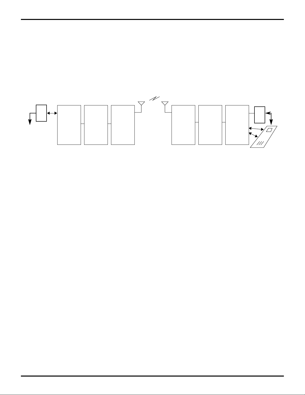
Figure 1. System Block Diagram of a Z87001/Z87010 Based Phone
optional microcontroller rather than by the Z87001’s DSP
core.
In combination with an RF section designed according to
the system specifications, Zilog’s Z87010/Z87L10 ADPCM
Processor, a standard 8-bit PCM telephone codec and
minimal additional phone circuity, the Z87001 and its embedded software provide a total system solution.
Codec
RF Section
Z87001
Spread
Spectrum
Controller
Z87010
ADPCM
Processor
Handset
P R E L I M I N A R Y
DS96WRL0800
1
Z87001/Z87L01
Zilog ROMless Spread Spectrum Cordless Phone Controller
RX
VREF
TX
RXSW
TXSW
PAON
RFEON
SYLE
RSSI
PWLV
ANT0
ANT1
HBSW
RESETB
TEST
ADC
(1-bit)
DAC
(4-bit)
ADC
(8-bit)
DAC
(4-bit)
FSK Demodulator
(downconverter, limiter discriminator,
AFC, bit sync, frame sync, SNR
detector)
FSK Modulator
256 Word
Frame Counter(s),
Event Trigger ,
T/R Switch Ctrl,
Power On/Off Ctrl,
Antenna Select
RAM 0
Receive
Rate
Buffer
Transmit
Rate
Buffer
DSP Core
256 Word
RAM 1
Z87010
Interface
Port 0
Port 1
Analog
Power
Digital
Power
VXDATA[7..0]
VXADD[2..0]
VXSTRB
VXRWB
VXRDYB
CLKOUT
CODCLK
P0[15..0]
P1[15..0]
Addr[15..0]
Data[15..0]
AVDD
AGND
VDD
GND
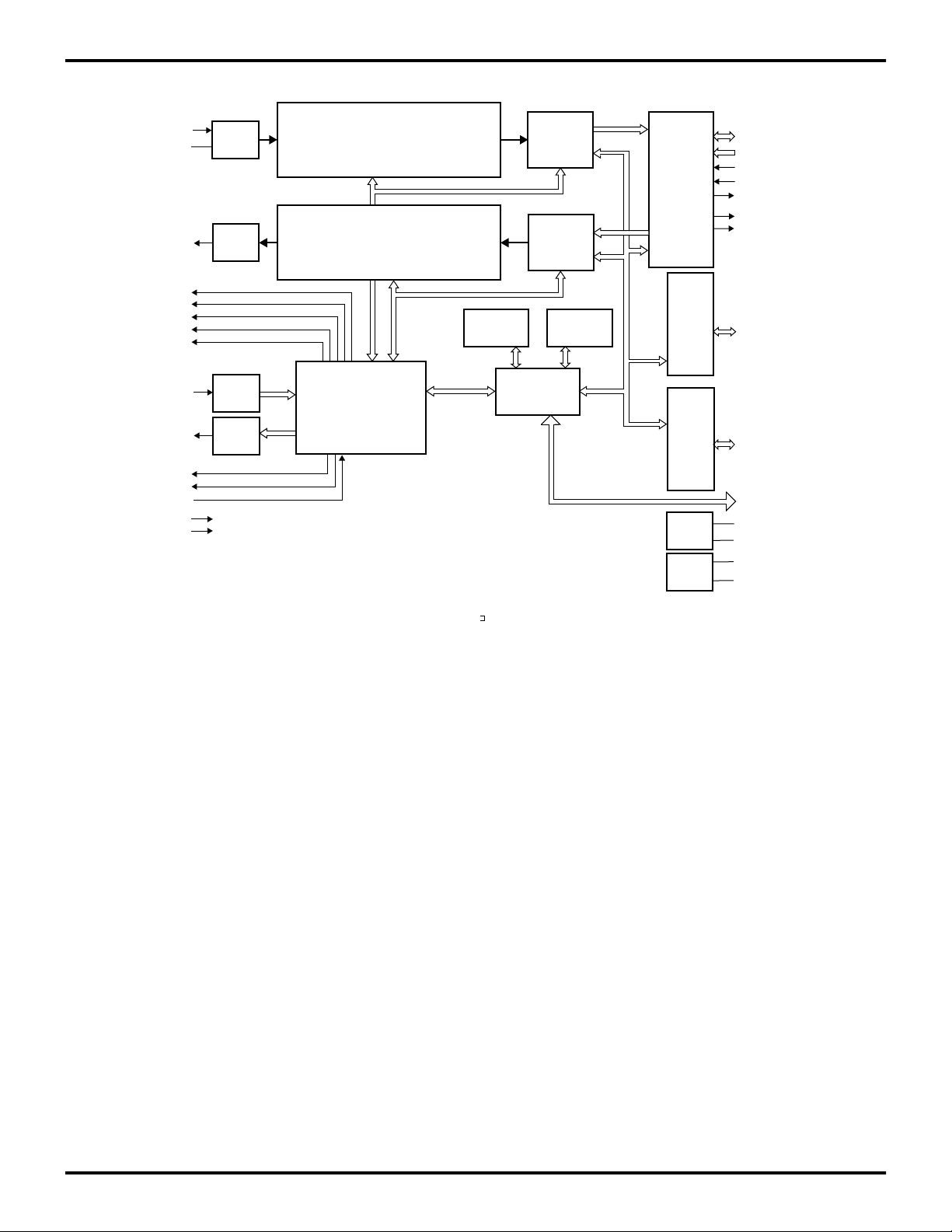
Figure 2. Z87001 Functional Block Diagram
DS96WRL0800
P R E L I M I N A R Y
3
4
Z87001/Z87L01
ROMless Spread Spectrum Cordless Phone Controller Zilog
PIN DESCRIPTION
AGND
RX
AVDD
VREF
RFEON
addr12
P115
addr11
GND
addr10
P114
addr9
P113
addr8
P112
addr7
VDD
addr6
P111
addr5
P110
addr4
P19
addr3
GND
addr2
P18
addr1
P17
addr0
P16
idata15
VDD
idata14
P15
TX
RSSI
AVDD
1
37
PWLV
AGND
TXSW
RXSW
addr13
addr14
dspclk
PAON
SYLE
addr15
VDD
triadd
halt
MCLK
intenb
GND
Z87001
RESETB
irwb
CODCLK
iaddr1
iaddr0
VXADD1
VXADD0
VXADD2
VDD
iaddr3
iaddr2
trice
VXRWB
iaddr4
eib
VXSTRB
GND
VXRDYB
109
73
VXDATA0
data0
VXDATA1
data1
VXDATA2
data2
VDD
VXDATA3
data3
VXDATA4
data4
VXDATA5
data5
VXDATA6
VXDATA7
data6
CLKOUT
data7
HBSW
data8
GND
TEST
VDD
data9
ANT0
data10
ANT1
data11
P00
P01
data12
GND
data13
P02
data14
P03
P14
idata13
P13
idata12
P12
GND
idata11
P11
idata10
P10
idata9
P015
idata8
VDD
P014
P013
idata7
idata6
P012
idata5
P011
P010
GND
idata3
idata4
P09
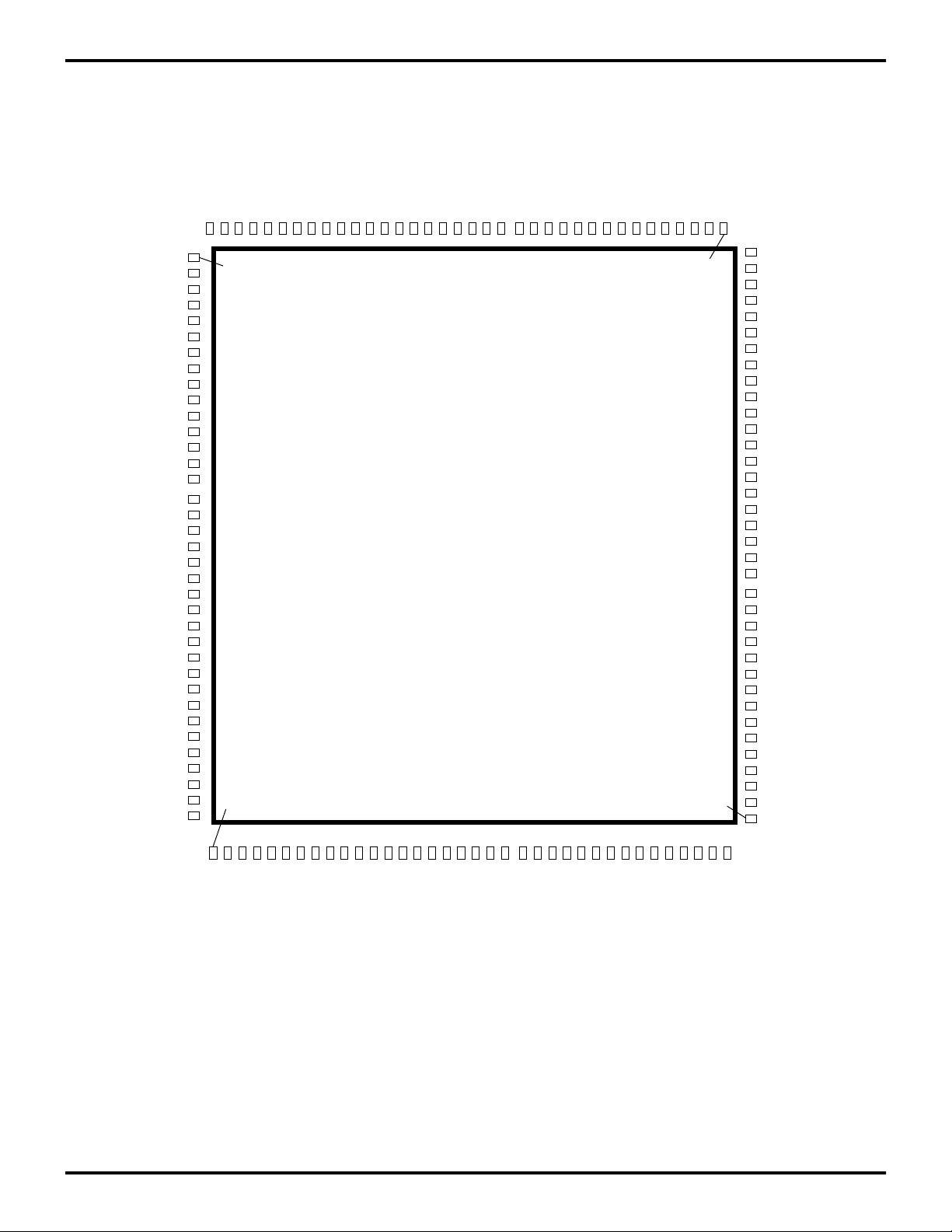
Figure 3. 144 Pin QFP Pin Configuration
P R E L I M I N A R Y
P07
P08
idata2
P06
VDD
idata1
P05
data15
idata0
P04
DS96WRL0800

1
Zilog ROMless Spread Spectrum Cordless Phone Controller
Table 1. 144 Pin QFP Pin Configuration
No Symbol Function Direction
1 TX Analog transmit IF signal Output
2,141 AGND Analog ground –
3 RX Analog receive IF signal Input
4,144 AV
5 VREF Analog reference voltage for RX signal –
6 RFEON RF on/off control Output
7,9,11,13,15,17,19,
21,23,25,27,29,31,
136,138,140
8,12,14,16,20,22,24,
28,30,32,36,37,39,
41,44,46
10,26,43,60,77,88,
109,128
18,34,51,68,86,102,
116,131
33,35,38,40,42,45,
47,49,52,54,56,59,
61,63,66,69
48,50,53,55,57,58,
62,64,65,67,70,72,
73,75,79,80
71,74,76,78,81,83,
85,89,91,93,96,98,
100,103,105,107
82,84 ANT[1..0] RF antenna diversity control Output
87 TEST Test mode select Input
90 HBSW Handset/base mode select Input
92 CLKOUT Clock, ADPCM processor (16.384 MHz) Output
94,95,97,99,101,
104,106,108
110 VXRDYB ADPCM processor ready Output
111 eib External register data strobe Output
112 VXSTRB ADPCM processor data strobe Input
113,117,119,121,
123
114 VXRWB ADPCM processor read/write control Input
115 trice ROMless mode select Input
118,120,122 VXADD[2..0] ADPCM processor address bus Input
124 CODCLK Clock to codec (2.048 MHz) Output
125 irwb External register read/write control Output
126 /RESETB Master reset Input
127 intenb Interrupt enable Input
VXDATA[7..0] ADPCM processor data bus Input
DD
addr[15..0] DSP core program address bus Output
P1[15..0] General-purpose I/O port 1 Input/Output
GND Digital ground –
V
DD
idata[15..0] DSP core internal data bus Output
P0[15..0] General-purpose I/O port 0 Input/Output
data[15..0] DSP core program data bus Input
iaddr[4..0] External register address bus Output
Analog power supply –
Digital power supply –
Z87001/Z87L01
DS96WRL0800
P R E L I M I N A R Y
5

6
Z87001/Z87L01
ROMless Spread Spectrum Cordless Phone Controller Zilog
PIN DESCRIPTION (Continued)
Table 1. 144 Pin QFP Pin Configuration
No Symbol Function Direction
129 halt Halt/ single step control Input
130 MCLK Master clock (16.384 MHz) Input
132 triadd Program address bus enable Input
133 PAON RF transmit enable Output
134 dspclk DSP core clock Output
135 SYLE RF synthesizer load enable Output
137 RXSW Demodulator “on” indication Output
139 TXSW RF receive enable Output
142 PWLV RF transmit power level Input
143 RSSI RF receive signal strength indicator Input
P R E L I M I N A R Y
DS96WRL0800
1
°
°
Z87001/Z87L01
Zilog ROMless Spread Spectrum Cordless Phone Controller
ABSOLUTE MAXIMUM RATINGS
Symbol Parameter Min Max Units
V
DD
, AV
DC Supply
DD
-0.5 7.0 V
Voltage(1)
V
V
T
IN
OUT
A
Input V oltage(2) -0.5 V
Output V oltage(3) -0.5 V
Operating
-20 +70
+ 0.5 V
DD
+ 0.5 V
DD
C
Temperature
T
STG
Storage
-65 +150
C
Temperature
Notes:
1. Voltage on all pins with respect to GND.
2. Voltage on all inputs WRT VDD
3. Voltage on all outputs WRT VDD
STANDARD TEST CONDITIONS
The electrical characteristics listed below apply for the following standard test conditions, unless otherwise noted.
All voltages are referenced to GND. Positive current flows
into the referenced pins. Standard test conditions are as
follows:
■
■
3.0V < V
4.5V < V
< 3.6V (Z87L01)
DD
< 5.5V (Z87001)
DD
Stresses greater than those listed under Absolute Maximum Ratings may cause permanent damage to the device. This is a stress rating only; operation of the device at
any condition above those indicated in the operational sections of these specifications is not implied. Exposure to absolute maximum rating conditions for extended period may
affect device reliability.
IoL
Threshold
Voltage
Output
Under
Test
GND = 0V
■
T
= -20 to +70 ° C
■
A
50pF
IoH
Figure 5. Test Load Diagram
DS96WRL0800
P R E L I M I N A R Y
7

8
Z87001/Z87L01
ROMless Spread Spectrum Cordless Phone Controller Zilog
RECOMMENDED OPERATING CONDITIONS
Table 3. 5V ± 0.5V Operation (Z87001)
Symbol Parameter Min Max Units
V
, AV
DD
DD
V
IH
V
IL
I
OH
I
OHICE
I
OL1
I
OL2
I
OLICE
T
A
Notes:
1. ICE pins are addr[15..0], iaddr[15..0], idata[15..0], eib and irwb
2. Maximum 3 pins total from P0[15..0] and P1[15..0]
Supply V oltage 4.5 5.5 V
Input High Voltage 2.0 V
+ 0.3 V
DD
Input Low Voltage GND -0.3 0.8 V
Output High Current -2.0 mA
Output High Current, ICE pins (1) -0.5 mA
Output Low Current 4.0 mA
Output Low Current, GPIO (limited usage, 2) 12.0 mA
Output Low Current, ICE pins (1) 0.5 mA
Operating Temperature -20 +70 °C
Table 4. 3.3V ± 0.3V Operation (Z87L01)
Symbol Parameter Min Max Units
V
DD
V
IH
V
IL
I
OH
I
OHICE
I
OL1
I
OL2
I
OLICE
T
A
Notes:
1. ICE pins are addr[15..0], iaddr[15..0], idata[15..0], eib and irwb
2. Maximum 3 pins total from P0[15..0] and P1[15..0]
Supply V oltage 3.0 3.6 V
Input High Voltage 0.7 V
DD
Input Low Voltage GND -0.3 0.1 V
VDD+0.3 V
DD
Output High Current -1.0 mA
Output High Current, ICE pins (1) -0.5 mA
Output Low Current 2.0 mA
Output Low Current, Ports (limited usage, 2) 6.0 mA
Output Low Current, ICE pins (1)) 0.5 mA
Operating Temperature -20 +70 °C
V
P R E L I M I N A R Y
DS96WRL0800

Z87001/Z87L01
1
Zilog ROMless Spread Spectrum Cordless Phone Controller
DC ELECTRICAL CHARACTERISTICS
Conditions for DC characteristics are corresponding operating conditions, and standard test conditions, unless otherwise specified.
Table 5. 5V ± 0.5V Operation (Z87001)
Symbol Parameter Test Condition Min Max Units
V
OH
V
OHICE
V
OL1
V
OL2
V
OLICE
I
L
I
CC
I
CC2
Notes:
1. ICE pins are addr[15..0], iaddr[15..0], idata[15..0], eib and irwb
2. Maximum 3 pins total from P0[15..0] and P1[15..0]
3. 2.3 mA typical at 25°C, 5 volts.
Output High Voltage VDD min, IOH max 2.4 V
Output High Voltage, ICE pins (1) VDD min, I
Output Low Voltage VDD min, I
Output Low Voltage, GPIO (2) VDD min, I
Output Low Voltage, ICE pins (1) VDD min, I
Input Leakage VIN = 0V, V
max 2.4 V
OHICE
max 0.6 V
OL1
max 1.2 V
OL2
max 0.4 V
OLICE
DD
-2 2 µA
Supply Current 80 mA
Standby Mode Current (3) 4 mA
Table 6. 3.3V ± 0.3V Operation (Z87L01)
Symbol Parameter Test Condition Min Max Units
V
OH
V
OHICE
V
OL1
V
OL2
V
OLICE
I
L
I
CC
I
CC2
Notes:
1. ICE pins are addr[15..0], iaddr[15..0], idata[15..0], eib and irwb
2. Maximum 3 pins total from P0[15..0] and P1[15..0]
3. 1.6 mA typical at 25°C, 3.3 volts.
Output High Voltage VDD min, IOH max 1.6 V
Output High Voltage, ICE pins (1)VDD min, I
Output Low Voltage VDD min, I
Output Low Voltage, Ports(2) VDD min, I
Output Low Voltage, ICE pins (1) VDD min, I
Input Leakage VIN = 0V, V
max 1.6 V
OHICE
max 0.4 V
OL1
max 1.2 V
OL2
max 0.4 V
OLICE
DD
-2 2 µA
Supply Current 55 mA
Standby Mode Current(2) 1.4 mA
DS96WRL0800 P R E L I M I N A R Y 9

Z87001/Z87L01
ROMless Spread Spectrum Cordless Phone Controller Zilog
ANALOG CHARACTERISTICS
Table 7. 1-Bit ADC (Temperature: -20/+70°C)
Parameter Minimum Typical Maximum Units
Resolution - 1 - bit
Power dissipation 0.54
(70°c)
Power dissipation, Stop mode 0.06
(70°c)
Sample frequency - 8.192 - MHz
Sample window(1) 29 31 33 ns
Bandwidth - 60 - MHz
Supply Range(=AVDD)
Z87L01
Z87001
3.0
4.5
Acquisition time 2 3 8 ns
Settling time 8 10 18 ns
Conversion time 4 6 18 ns
Aperture delay 2 3 8.5 ns
Aperture uncertainty(2) - - 0.5 ns
Input voltage range (p-p) 800 1000 1200 mV
Reference voltage
Z87L01
Z87001
1.7 (AV
2.7 (AV
DD
DD
= 3V)
=4.5V)
1.9 (AV
Input resistance 10 18 25 KOhm
Input capacitance - 10 - pF
Notes:
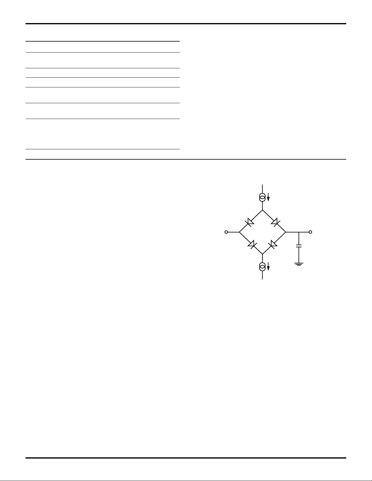
Window of time while input signal is applied to sampling capacitor; see next figure.
Uncertainty in sampling time due to random variations such as thermal noise.
(40°c)
(40°c)
3.0 (AV
1.0
0.2
DD
DD
= 3.3V)
= 5V)
(-20°c)
(-20°c)
2.1 (AV
3.3 (AV
2.75
1.1
3.6
5.5
DD
DD
= 3.6V)
= 5.5V)
mW
mW
V
V
V
V
10 P R E L I M I N A R Y DS96WRL0800
Z87001/Z87L01
1
Zilog ROMless Spread Spectrum Cordless Phone Controller
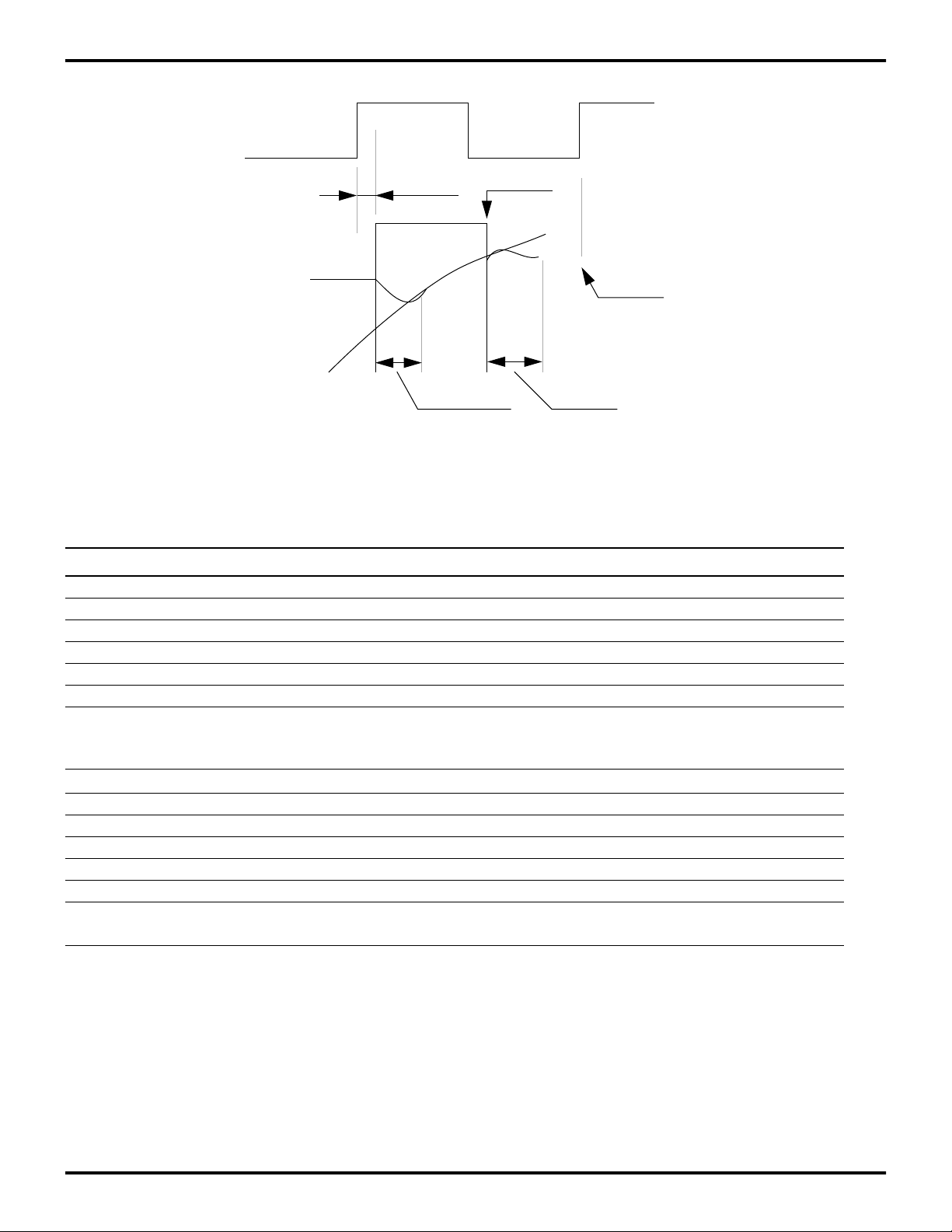
CLK (16.384MHz)
Aperture
Delay
SAMPLING
WINDOW
INPUT
SIGNAL
Sampling
Latched
Output
Acquisition
Time
Settling
Time
Conversion
+
Time (for
digital output)
Figure 6. 1-Bit ADC Definition of Terms
Table 8. 8-bit ADC (Temperature -20/+70°C)
Parameter Minimum Typical Maximum Units
Resolution - 6 - bit
Integral non-linearity - 0.5 1 LSB
Differential non-linearity - - 0.5 LSB
Power Dissipation (peak) 35 70 mW
Sample window 5 - 120 ns
Bandwidth - - 2 Msps
Supply Range (=AVDD)
Z87L01
Z87001
3.0
4.5
Input voltage range 0-AV
3.3
5.0
DD
3.6
5.5
V
V
V
Conversion time 0.5 - - µs
Aperture delay 2 3 8.5 ns
Aperture uncertainty - - 1 ns
Input resistance - 25 - Kohm
Input capacitance - 10 - pF
Notes:
1. 8-bit ADC only tested for 6-bit resolution.
DS96WRL0800 P R E L I M I N A R Y 11

Z87001/Z87L01
ROMless Spread Spectrum Cordless Phone Controller Zilog
Table 9. 4-bit DAC (Temperature: -20/+70°C)
Parameter Minimum Typical Maximum Units
Resolution - 4 - bit
Integral non-linearity - 0.25 0.5 LSB
Differential non-linearity - 0.25 1 LSB
Settling time (1/2 LSB) - - 22.5 ns
Zero error at 25°C-12mV
Conversion time (input change to output change) 14 19 76 ns
Power dissipation, 25 pF load 1.2
(70°c)
Power dissipation, 25 pF load, Stop mode 0.18
(70°c)
20
(40°c)
1.0
(40°c)
24.1
(-20°c)
1.1
(-20°c)
mW
mW
Conversion time (input change to output change) 14.5 19.1 75.8 ns
Rise time (full swing) 11 15 71 ns
Output slew rate 8 67 96 V/µs
Output voltage range - 0.2 AV
Supply Range (=AV
Z87L01
Z87001
DD
)
3.0
4.5
to 0.6A V
DD
3.3
5.0
DD
-V
3.6
5.5
V
V
Output load resistance 330 Ohm
Output load capacitance - 25 - pF
12 P R E L I M I N A R Y DS96WRL0800

Z87001/Z87L01
1
Zilog ROMless Spread Spectrum Cordless Phone Controller
INPUT/OUTPUT PIN CHARACTERISTICS
All digital pins (all pins except VDD, AVDD, GND, AGND,
V
, RX, TX, RSSI and PWLV) have an internal capaci-
REF
tance of 5 pF.
The RX analog input pin has an input capacitance of 10
pF.
The RSSI analog input pin has an input capacitance of 10
pF.
AC ELECTRICAL CHARACTERISTICS
Clocks, Reset and RF Interface
Table 10. Clocks, Reset and RF Interface
No. Symbol Parameter Min Max Units
1 TpC MCLK input clock period (1) 61 61 ns
2 TwC MCLK input clock pulse width 20 40 ns
3 TrC, TfC MCLK input clock rise/fall time 15 ns
4 TrCC, TfCC CLKOUT output clock rise/fall time 2 6 ns
5 TrCO, TfCO CODCLK output clock rise/fall time 2 6 ns
6 TwR RESETB input low width 18 TpC
7 TrRF, TfRF RF output controls rise/fall time (2) 2 6 ns
Notes:
1. MCLK is 16.384 MHz ± 25 ppm
2. RF Controls are PAON, TXSW, RFEON, SYLE.
DS96WRL0800 P R E L I M I N A R Y 13

Z87001/Z87L01
ROMless Spread Spectrum Cordless Phone Controller Zilog
ADPCM Processor Interface
The Z87001 is a peripheral device for the ADPCM Processor. The interface from the Z87001 perspective is composed of an input address bus, a bidirectional data bus,
strobe and read/write input control signals and a
READ CYCLES refer to data transfers from the Z87001 to
the ADPCM Processor.
WRITE CYCLES refer to data transfers from the ADPCM
Processor to the Z87001.
ready/wait output control signal.
Table 11. Read Cycles
Signal Name Function Direction
VXADD[2..0] Address Bus ADPCM Proc. to Z87001
VXDATA[7..0] Data Bus Bidirectional
VXSTRB Strobe Control Signal ADPCM Proc. to Z87001
VXRWB Read/Write Control Signal ADPCM Proc. to Z87001
VXRDYB Ready Control Signal Z87001 to ADPCM Proc.
Table 12. Write Cycles
No. Symbol Parameter Min Max Units
8 TsAS Address, Read/Write setup time before Strobe falls 10 ns
9 ThSA Address, Read/Write hold time after Strobe rises 3 ns
10 TaDrS Data read access time after Strobe falls 30 (1) ns
11 ThDrS Data read hold time after Strobe rises 8.5 40 (2) ns
12 TwS Strobe pulse width 20
13 TsDwS Data write setup time before Strobe rises 10 ns
14 ThDwS Data write hold time after Strobe rises 3 ns
15 TaDrRY Data read valid before Ready falls 22 ns
16 TdSRY Strobe high after Ready falls 0 ns
Notes:
1. Requires wait state on ADPCM Processor read cycles
2. Requires no write cycle directly following read cycle on ADPCM Processor
14 P R E L I M I N A R Y DS96WRL0800
Z87001/Z87L01
1
Zilog ROMless Spread Spectrum Cordless Phone Controller
AC TIMING DIAGRAMS
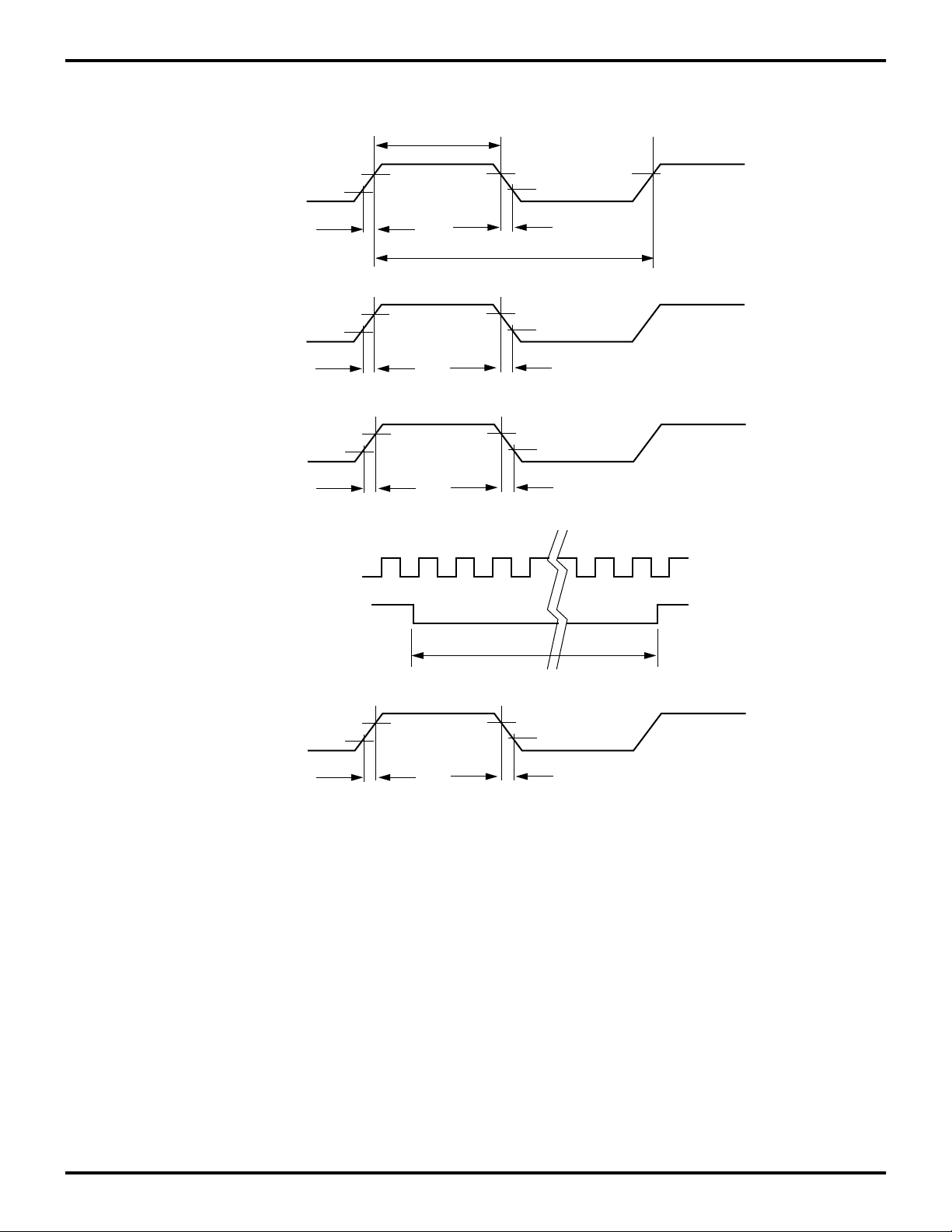
TwC(2)
MCLK
TfC(3)TrC(3)
TpC (1)
CLKOUT
CODCLK
MCLK
RESETB
PAON
TXSW
RXSW
RFEON
SYLE
TrCC(4)
TrCO(5)
TrRF(7)
1
TfCC(4)
TfCO(5)
23
TwR(6)
TfRF(7)
418
16
17
Figure 7. Transceiver Output Signal
DS96WRL0800 P R E L I M I N A R Y 15

Z87001/Z87L01
ROMless Spread Spectrum Cordless Phone Controller Zilog
TsAS(8) ThSA(9)
VXADD
VXRWB
VXSTRB
ThDrS(11)TaDrS(10)
VXDA TA
VXRD YB
VXDATA Read Cycle
VXADD
VXRWB
VXSTRB
VXDATA
VXRDYB
TsAS(8) ThSA(9)
TwS(12)
ThDwS(14)
TsDwS(13)
VXDA TA Write Cycle
Figure 8. Read/Write Cycle TImings
16 P R E L I M I N A R Y DS96WRL0800
 Loading...