ZILOG Z86E0308PSC, Z86E0308SSC, Z86E0612PSC, Z86E0612SSC Datasheet

1
Z86E03/E06
CP95DZ81301
PRELIMINARY
CP95DZ81301 (8/95)
P
RELIMINARY
C
USTOMER PROCUREMENT SPECIFICATION
FEATURES
GENERAL DESCRIPTION
The Z86E03/E06 are One-Time Programmable (OTP)
members of the Z8® microcontroller family allowing easy
software development, debug, and prototyping for small
production runs that are not economically desirable with a
masked ROM version.
Three address spaces, the Program Memory, Register
File, and Expanded Register File (ERF), support a wide
range of memory configurations. Through the ERF, the
designer has access to four additional control registers
that provide extra peripheral devices, I/O ports, register
addresses, an SPI receive buffer and SPI compare
register.
ROM RAM* Speed
Part (Kbytes) (Kbytes) SPI (MHz)
Z86E03 512 61 No 8
Z86E06 1 125 Yes 12
Z86E03/E06
CMOS Z8® OTP
MICROCONTROLLERS
For applications demanding powerful I/O capabilities, the
Z86E03/E06's dedicated input and output lines are grouped
into two ports, and are configurable under software control
to provide timing, status signals, or parallel I/O.
Notes:
All Signals with a preceding front slash, "/", are active Low, e.g.:
B//W (WORD is active Low); /B/W (BYTE is active Low, only).
Power connections follow conventional descriptions below:
Connection Circuit Device
Power V
CC
V
DD
Ground GND V
SS
*General-Purpose
■ 18-Pin DIP, WIN, and SOIC Packages
■ 4.5- to 5.5-Volt Operating Range
■ 0°C to +70°C Temperature Range
■ Low-Power Consumption
■ Expanded Register File (ERF)
■ 14 Input/Output Lines
■ Serial Peripheral Interface (SPI) (Z86E06 Only)
■ Software Watch-Dog Timer (WDT)
■ Power-On Reset (POR)

2
Z86E03/E06
CP95DZ81301
PRELIMINARY
GENERAL DESCRIPTION (Continued)
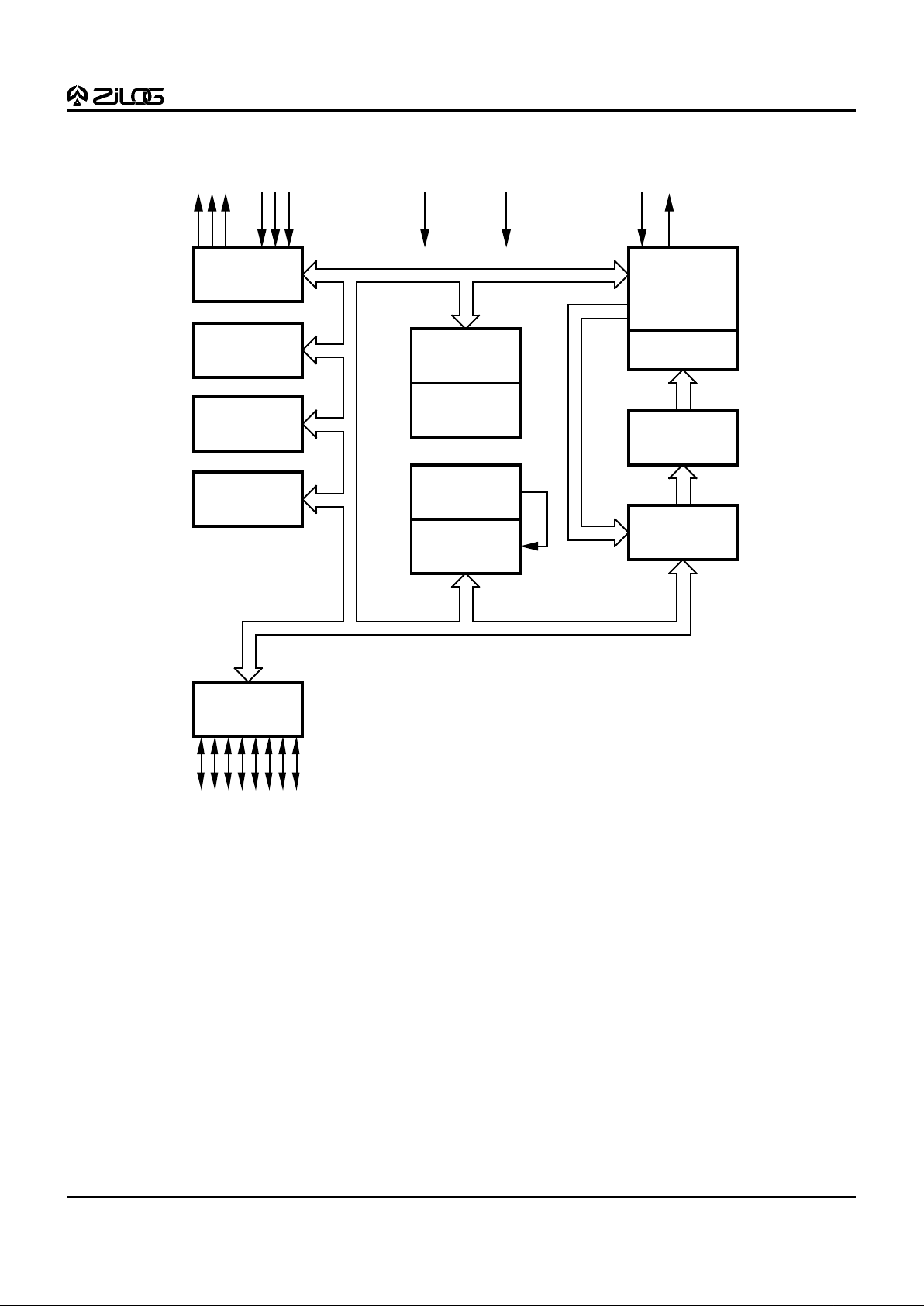
Port 3
Counter/
Timer
Interrupt
Control
T wo Analog
Comparators
Port 2
I/O
(Bit Programmable)
ALU
FLAG
Register
Pointer
Register File
142 x 8-Bit*
Vcc GND XTAL
InputOutput
Machine
Timing & Inst.
Control
Prg. Memory
1K x 8-Bit*
Program
Counter
WDT, POR
Note:
*The Z86E03 has 512 x 8-Bit Program
Memory and 78 x 8-Bit Register File.
Functional Block Diagram

3
Z86E03/E06
CP95DZ81301
PRELIMINARY
GENERAL DESCRIPTION (Continued)
1
2
9
3
4
5
6
7
8
18
17
16
15
14
13
12
11
10
D3
D2
VPP
D1
D0
GND
/PGM
CLOCK
CLEAR
D4
D5
EPM
D6
D7
Vcc
N/C
/CE
/OE
Z86E03/E06
EPROM
1
2
9
3
4
5
6
7
8
18
17
16
15
14
13
12
11
10
P23
P22
P33
P21
P20
GND
P36
P35
P34
P24
P25
P32
P26
P27
Vcc
XTAL2
XTAL1
P31
Z86E03/
E06
PDIP
18-Pin DIP/WIN
Pin Configuration
18-Pin EPROM Mode
Pin Configuration
18-Pin Identification
Pin # Symbol Function Direction
1-4 P24-P27 Port 2, Pins 4,5,6,7 Input/Output
5VCCPower Supply
6 XTAL2 Crystal Oscillator Clock Output
7 XTAL1 Crystal Oscillator Clock Input
8-10 P31-P33 Port 3, Pins 1,2,3 Fixed Input
11-13 P34-P36 Port 3, Pins 4,5,6 Fixed Output
14 GND Ground
15-18 P20-23 Port 2, Pins 0,1,2,3 Input/Output
 Loading...