FEATURES
PRELIMINARY
P
RELIMINARY
C
USTOMER
P
Z86217/C17
CMOS Z8® 8-BIT MICROCONTROLLERS
(POINTING DEVICE/TRACKBALL)
Z86217/C17
CP95KEY1000
ROCUREMENT SPECIFICATION
Part ROM RAM* I/O Speed
Number (Kbytes) (Bytes) Lines (MHz)
Z86217 2 124 14 4
Z86C17 2 124 14 4
* General-Purpose
■ 18-Pin DIP and SOIC Packages
■ 3.0- to 5.5-Volt Operating Range
■ 0°C to 70°C Operating Temperature Range
GENERAL DESCRIPTION
The Z86217/C17 are members of Zilog's Z8® family of
microcontrollers designed to reduce external system components and offer easy software/hardware development
tools for pointing device and trackball applications.
The devices feature on-board pull-up resistors, and a
scalable trip-point buffer to accommodate opto-transistor
outputs. The high drive ports are capable of up to 20 mA
(at VOL = 0.8-volt) current sinking per pin, with three pins
maximum, providing extra sinking current capability.
The Z86217/C17's permanently enabled Watch-Dog Timer
(WDT) operates upon power-up of the MCU, and provides
added operational reliability for pointing device and
trackball environments.
■ Permanent Watch-Dog Timer (WDT)
■ Oscillator Filter
■ Two Programmable 8-Bit Counter/Timers
■ Low-EMI Operation
■ Scalable Trip-Point Buffer
■ On-Board Pull-Up Resistors
■ High Drive Ports Can Sink 20 mA Per Pin, with Three
Pins Maximum
Two on-chip counter/timers with a large number of
selectable modes, offload the system of administering
real-time tasks such as counting/timing and I/O data
communications.
Notes:
Refer to the DC electrical characteristics for detailed specification of the
sinking current.
On the Z86C17, P24-P27 has a 20K pull-up, and P32 has a 47K pulldown. The Z86217 does not have these functions.
All Signals with a preceding front slash, "/", are active Low, e.g.; B//W
(WORD is active Low); /B/W (BYTE is active Low, only).
Power connections follow conventional descriptions below:
Connection Circuit Device
An oscillator filter assists in separating out high-frequency
noise from the oscillator input pin.
CP95KEY1000 8/95
Power V
Ground GND V
CC
V
DD
SS
1

PRELIMINARY
Z86217/C17
CP95KEY1000
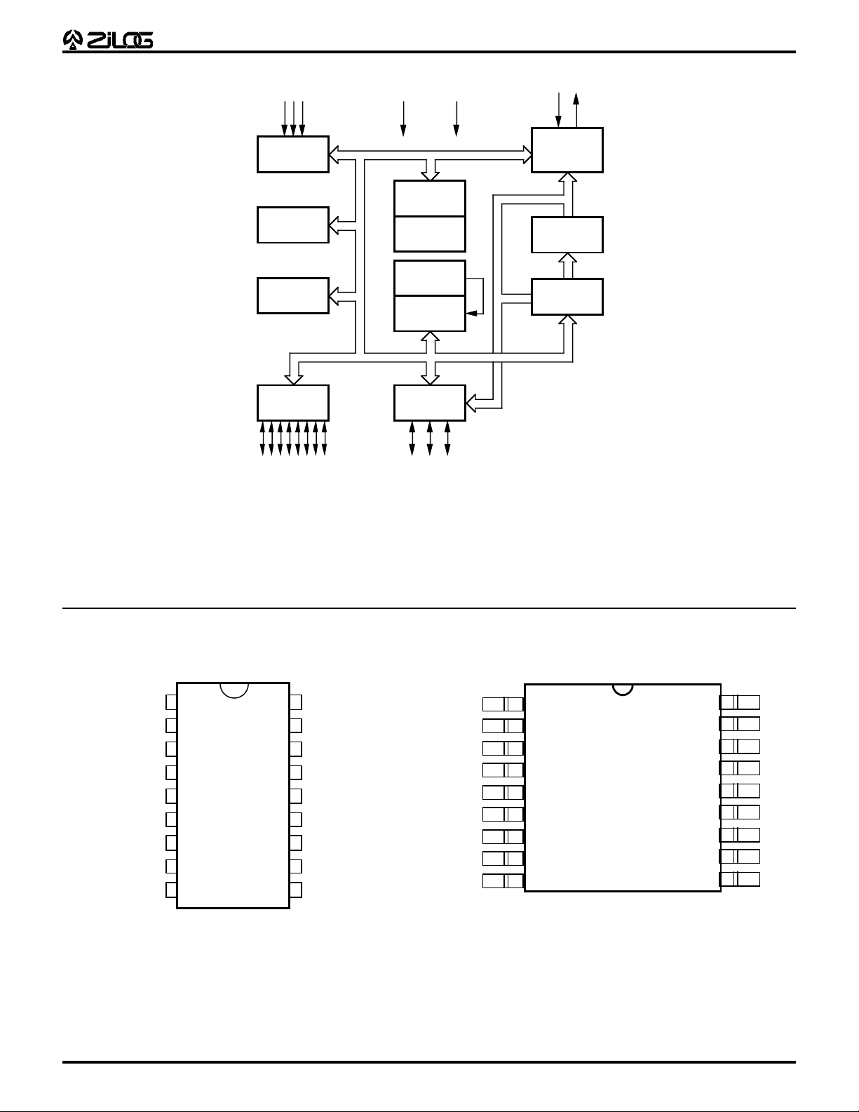
BLOCK DIAGRAM
Input
Port 3
Counter/
Timers (2)
Interrupt
Control
Port 2
I/O
(Bit Programmable)
VDD
ALU
FLAG
Register
Pointer
Register File
144 x 8-Bit
Port 0
I/O
VSS
XTAL
Machine
Timing & Inst.
Control
Prg. Memory
2048 x 8-Bit
Program
Counter
PIN DESCRIPTIONS
P24
P25
P26
P27
VDD
XTAL2
XTAL1
P31
P32
1
2
3
4
5
6
7
8
9
18
17
16
15
14
13
12
11
10
Functional Block Diagram
P23
P22
P21
P20
VSS
P02
P01
P00
P33
XTAL2
XTAL1
P24
P25
P26
P27
VDD
P31
P32
118
2
3
4
5
6
7
8
9
17
16
15
14
13
12
11
10
P23
P22
P21
P20
VSS
P02
P01
P00
P33
18-Pin DIP Configuration
18-Pin SOIC Configuration
2

ABSOLUTE MAXIMUM RATINGS
PRELIMINARY
Z86217/C17
CP95KEY1000
Sym Parameter Min Max Units
V
T
T
Notes:
* Voltages on all pins with respect to GND
† See Ordering Information
DD
STG
A
Supply Voltage (*) –0.3 +7 V
Storage Temp –65° +150° C
Oper Ambient Temp † † C
STANDARD TEST CONDITIONS
The characteristics listed below apply for standard test
conditions as noted. All voltages are referenced to GND.
Positive current flows into the referenced pin (Test Load).
Stress greater than those listed under Absolute Maximum
Ratings may cause permanent damage to the device. This
is a stress rating only; operation of the device at any
condition above those indicated in the operational sections of these specifications is not implied. Exposure to
absolute maximum rating conditions for extended periods
may affect device reliability.
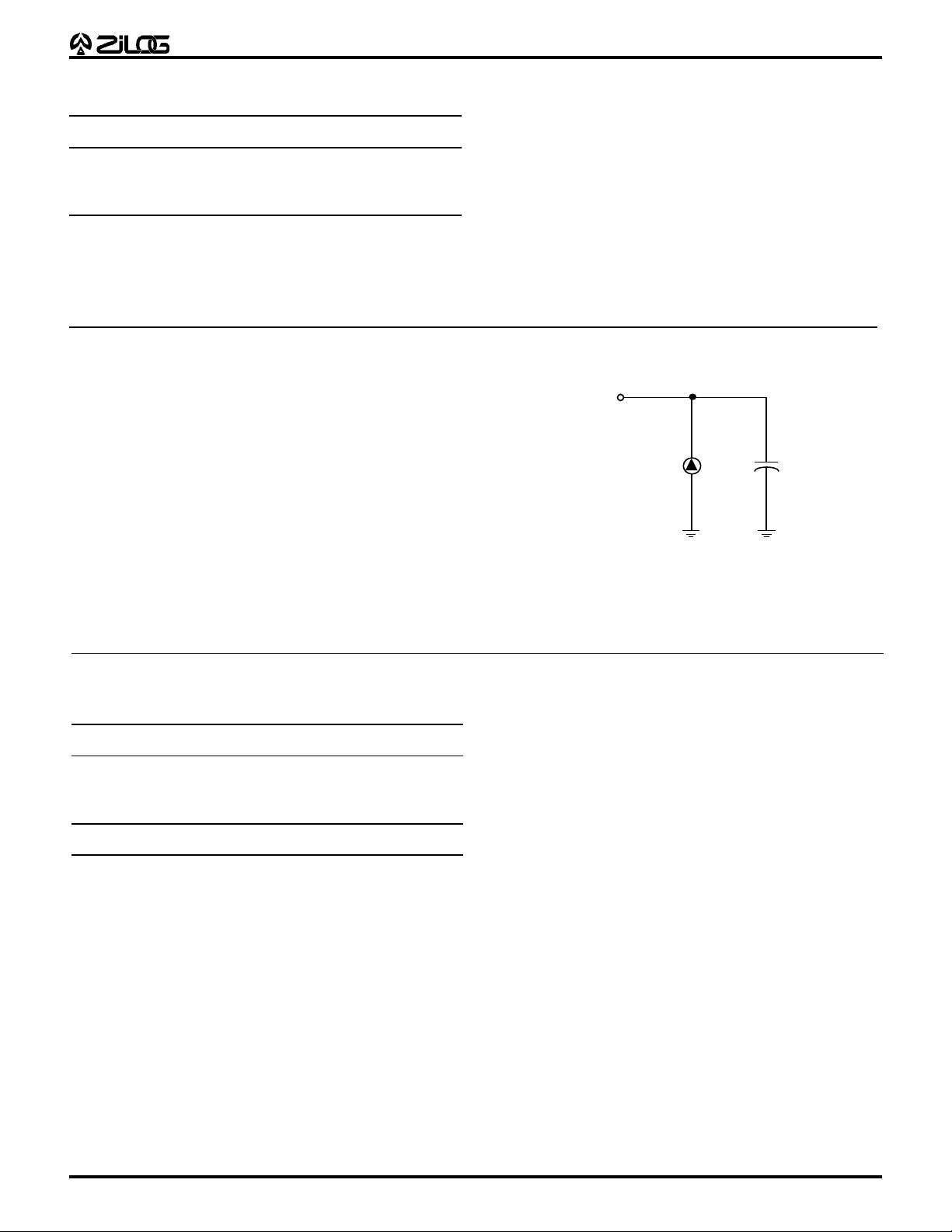
From Output
Under Test
150 pFI
CAPACITANCE
TA = GND = 0V, f = 1.0 MHz, unmeasured pins to GND
Parameter Max
Input capacitance 10 pF
Output capacitance 20 pF
I/O capacitance 25 pF
Vdd SPECIFICATION
Vdd = 3.0V to 5.5V
Test Load Diagram
3
 Loading...