

ZILOG Z8018520FSC, Z8018533FSC, Z8019520FSC, Z8019533FSC Datasheet

Zilog
FEATURES
PRELIMINARY
P
RELIMINARY PRODUCT SPECIFICATION
Z80185/Z80195
SMART PERIPHERAL CONTROLLERS
SMART PERIPHERAL CONTROLLES
Z80185/Z80195
ROM UART Speed
Part (KB) Baud Rate (MHz)
Z80185 32 x 8 512 Kbps 20, 33
Z80195 0 512 Kbps 20, 33
■ 100-Pin QFP Package
■ 5.0-Volt Operating Range
■ Low-Power Consumption
■ 0°C to +70°C Temperature Range
GENERAL DESCRIPTION
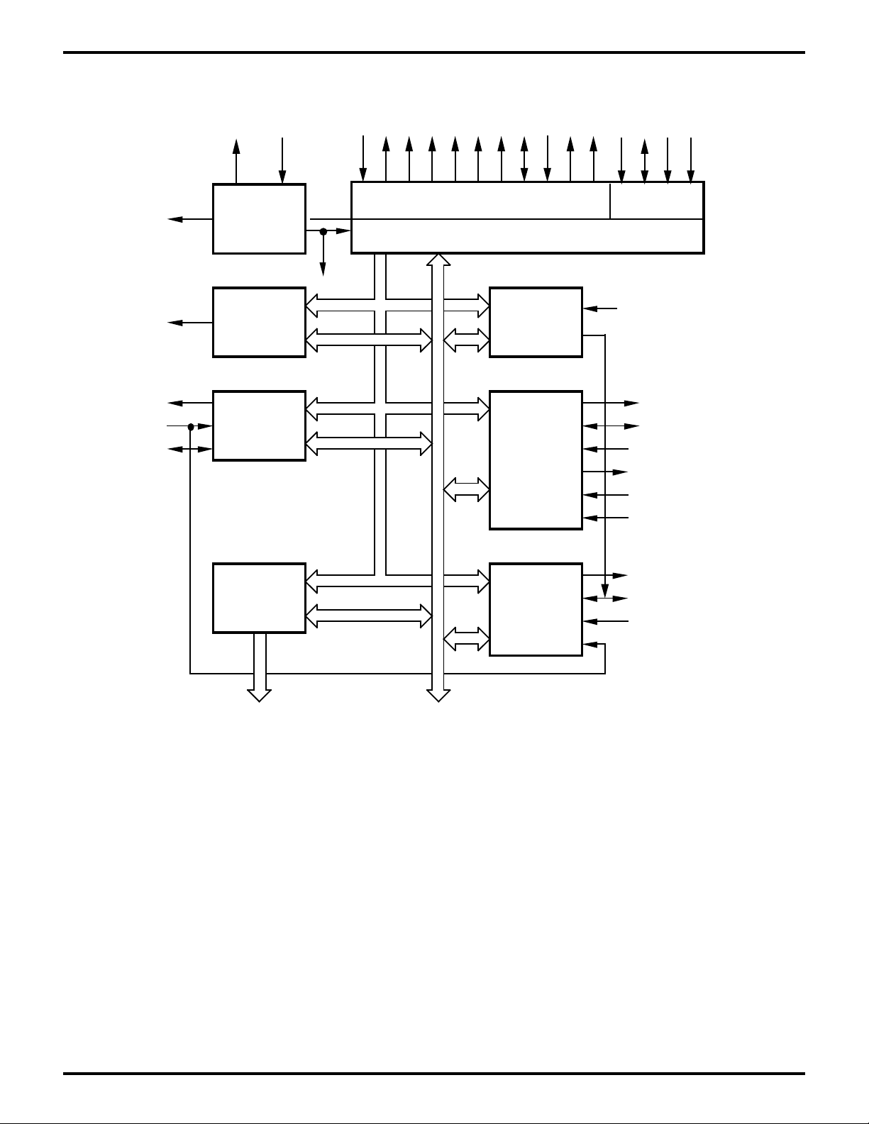
The Z80185 and Z80195 are smart peripheral controller
devices designed for general data communications applications, and architected specifically to accommodate all
input and output (I/O) requirements for serial and parallel
connectivity. Combining a high-performance CPU core
with a variety of system and I/O resources, the Z80185/195
are useful in a broad range of applications. The Z80195 is
the ROMless version of the device.
The Z80185 and Z80195 feature an enhanced Z8S180
microprocessor linked with one enhanced channel of the
Z85230 ESCC™ serial communications controller, and 25
bits of parallel I/O, allowing software code compatibility
with existing software code.
■ Enhanced Z8S180 MPU
■ Four Z80 CTC Channels
■ One Channel ESCC™ Controller
■ Two 8-Bit Parallel I/O Ports
■ Bidirectional Centronics Interface (IEEE 1284)
■ Low-EMI Option
Seventeen lines can be configured as bidirectional
Centronics (IEEE 1284) controllers. When configured as a
1284 controller, an I/O line can operate in either the host or
peripheral role in compatible, nibble, byte or ECP mode. In
addition, the Z80185 includes 32 Kbytes of on-chip ROM.
These devices are well-suited for external modems using
a parallel interface, protocol translators, and cost-effective
WAN adapters. The Z80185/195 is ideal for handling all
laser printer I/O, as well as the main processor in costeffective printer applications.
Notes:
All Signals with a preceding front slash, "/", are active Low.
DS971850301
Power connections follow conventional descriptions below:
Connection Circuit Device
Power V
Ground GND V
CC
V
DD
SS
1
Zilog
TIMING DIAGRAMS (Continued)
PRELIMINARY
SMART PERIPHERAL CONTROLLERS
Z80185/Z80195
Processor
Power Controller
TxD,
RxD
TOUT
16-Bit Address Bus
8-Bit Data Bus
EMSCC
Parallel Ports (2)
Including IEEE
Bidirectional
Centronics Controller
16-Bit Programmable
Reload Timers (2)
MMU A19-0
Decode
DMACs (2)
ROM
32K x 8
(Z80185 Only)
UARTs (2)
TXA1-0,
RXA1-0
/ROMCS
/RAMCS
CLK/TRG ZC/TO
Figure 1. Z80185/195 Functional Block Diagram
CTCs (4)
2
DS971850301
Zilog
PIN DESCRIPTION
/INT0
/NMI
PRELIMINARY
/RESET
/BUSREQ
/BUSACK
/WAIT
EXTAL
XTAL
VSS
A17
PHI
/RD
/WR
/M1
NFAULT
/MREQ
/IORQ
/RFSH
VDD
SMART PERIPHERAL CONTROLLES
Z80185/Z80195
/HALT
/INT1
/INT2
ST
A15
A5
A7
A9
A10
A11
A12
VSS
A13
A14
A16
D0
D4
D5
/RAMCS
A0
A1
A2
A3
A4
A6
A8
D1
D2
D3
D6
D7
100
1
95
90
85
5
10
15
Z80185/Z80195
100-Pin QFP
20
25
30
80
75
70
65
60
55
50454035
NSTROBE
NACK
NAUTOFD
TOUT//DREQ
BUSY
NINIT
RXA1
/IOCS
TXA1
CKA0/CKS
RXA0
TXA0
/DCD0/CKA1
/CTS0/RXS
/RTS0/TXS
A18
A19
VSS
IEI
/ROMCS
IEO
VSS
/DCD
/CTS
/RTS
/DTR
TXD
/TRXC
RXD
PERROR
DS971850301
VSS
PIA11/CLKTRG1
PIA12/CLKTRG2
PIA10/CLKTRG0
PIA13/CLKTRG3
PIA14/ZCTO0
PIA15/ZCTO1
VDD
SELECT
PIA16/ZCTO2
PIA20
PIA21
PIA22
Figure 2. 100-Pin QFP Pin Assignments
PIA23
PIA24
PIA25
PIA26
PIA27
/RTXC
NSELECTIN
3
Zilog
ABSOLUTE MAXIMUM RATINGS
PRELIMINARY
SMART PERIPHERAL CONTROLLERS
Z80185/Z80195
Symbol Description Min Max Units
V
CC
V
IN
T
OPR
T
STG
Notes:
Voltage on all pins with respect to GND. Permanent LSI damage may
occur if maximum ratings are exceeded. Normal operation should be
recommended operating conditions. If these conditions are exceeded, it
could affect reliability of LSI.
Supply Voltage –0.3 +7.0 V
Input Voltage –0.3 VCC+0.3 V
Operating Temp. 0 70 °C
Storage Temp. –55 +150 °C
STANDARD TEST CONDITIONS
The DC Characteristics and capacitance sections below
apply for the following standard test conditions, unless
otherwise noted. All voltages are referenced to GND (0V).
Positive current flows into the referenced pin (Test Load).
Operating Temperature Range:
S = 0°C to 70°C
Voltage Supply Range:
+4.5V ≤ VCC ≤ +5.5V
Stresses greater than those listed under Absolute Maximum Ratings may cause permanent damage to the device. This is a stress rating only; operation of the device at
any condition above those indicated in the operational
sections of these specifications is not implied. Exposure to
absolute maximum rating conditions for extended periods
may affect device reliability.
= 2 mA
I
OL
1.4 V
All AC parameters assume a load capacitance of 100 pF.
Add 10 ns delay for each 50 pF increase in load up to a
maximum of 150 pF for the data bus and 100 pF for
address and control lines. AC timing measurements are
referenced to 1.5 volts (except for clock, which is referenced to the 10% and 90% points). Maximum capacitive
load for PHI is 125 pF.
100 pF
= 250 µA
I
OH
Figure 3. Test Load Diagram
4
DS971850301

Zilog
PRELIMINARY
DC CHARACTERISTICS
VDD = 5.0V ±10%, VSS = 0V over specified temperature range, unless otherwise noted.
Symbol Item Condition Min. Typ. Max. Unit
SMART PERIPHERAL CONTROLLES
Z80185/Z80195
V
IH
V
IL
V
OH
V
OL1
I
IL
Input “H” Voltage † V
Input “L” Voltage † V
Output “H” Voltage † V
Output “L” Voltage † V
Input Leakage VIN=0.5 to
Current All Inputs VDD–0.5 1.0
Except XTAL,EXTAL µA
I
TL
Tri-State Leakage VIN=0.5 to
Current VDD–0.5 1.0 µA
VDD Supply Current*
Normal Operation
For 5.0V: f = 20 MHz 60 120 mA
For 5.0V: f = 33 MHz 68 132 mA
ICC* Power Dissipation*
System Stop Mode
For 5.0V: f = 20 MHz 5 10 mA
For 5.0V: f = 33 MHz 7 13 mA
Notes:
† See Class Reference Table
* V
min = VDD –1.0V, VIL max = 0.8V (All output terminals are at no load.)
IH
DS971850301
5
Zilog
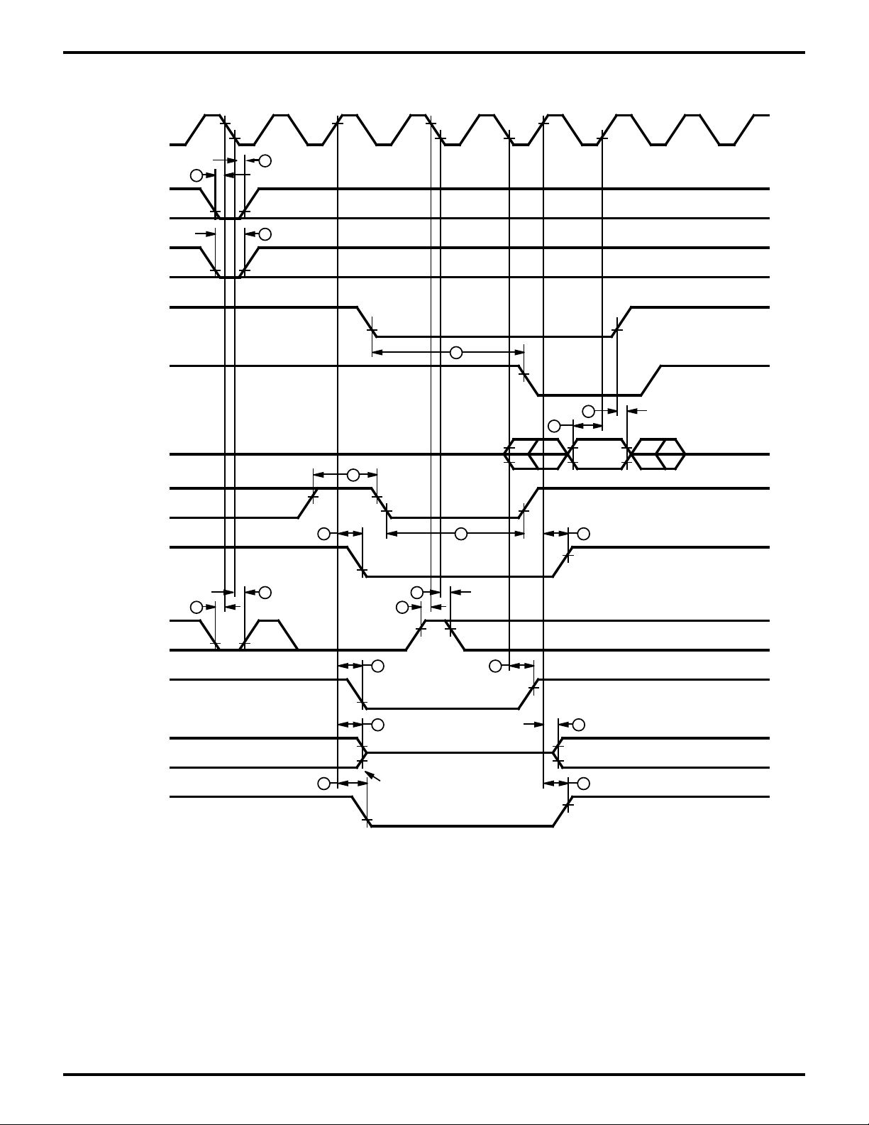
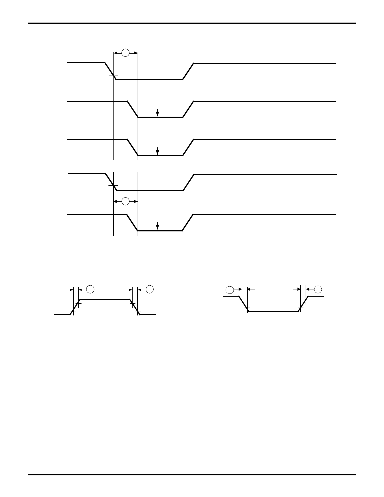
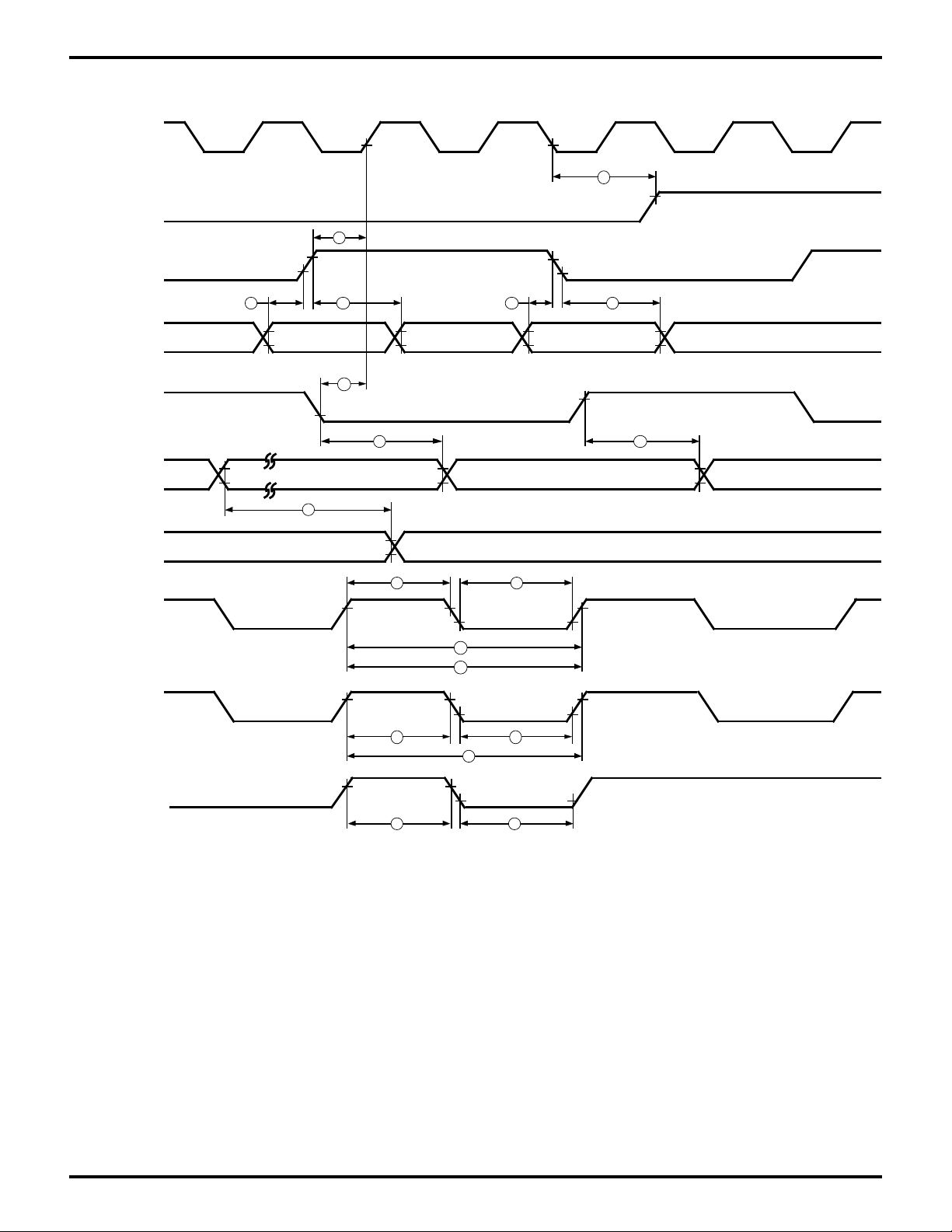
TIMING DIAGRAMS
Z8S180 MPU Timing
PRELIMINARY
SMART PERIPHERAL CONTROLLERS
Z80185/Z80195
ø
Address
/WAIT
/MREQ
/IORQ
/RD
/WR
Opcode Fetch Cycle
I/O Write Cycle †
I/O Read Cycle †
T1 T2 TW T3 T1 T2 TW T3 T1
5
4
32
1
6
19
20
19
7
8
9b
9a
14
12
20
13
11
7
28b
11
28a
9
22
29
13
25
26 and 26a
11
11
/M1
ST
Data
IN
Data
OUT
/RESET
54
48
10
17
49
53
18
15
16
23
Figure 4. CPU Timing
(Opcode Fetch Cycle, Memory Read/Write Cycle
I/O Read/Write Cycle)
24
15
16
21
27
49
48
54
53
6
DS971850301
Zilog
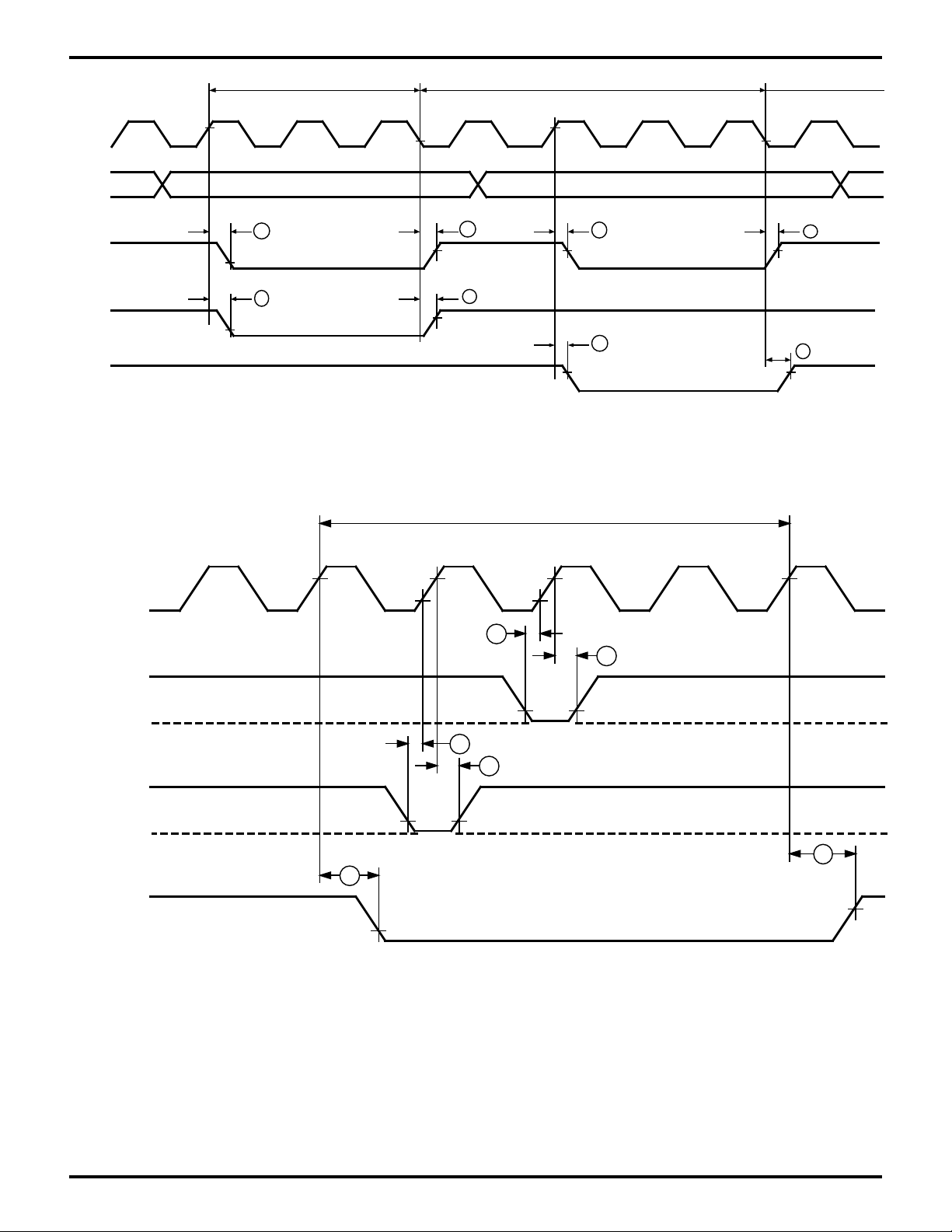
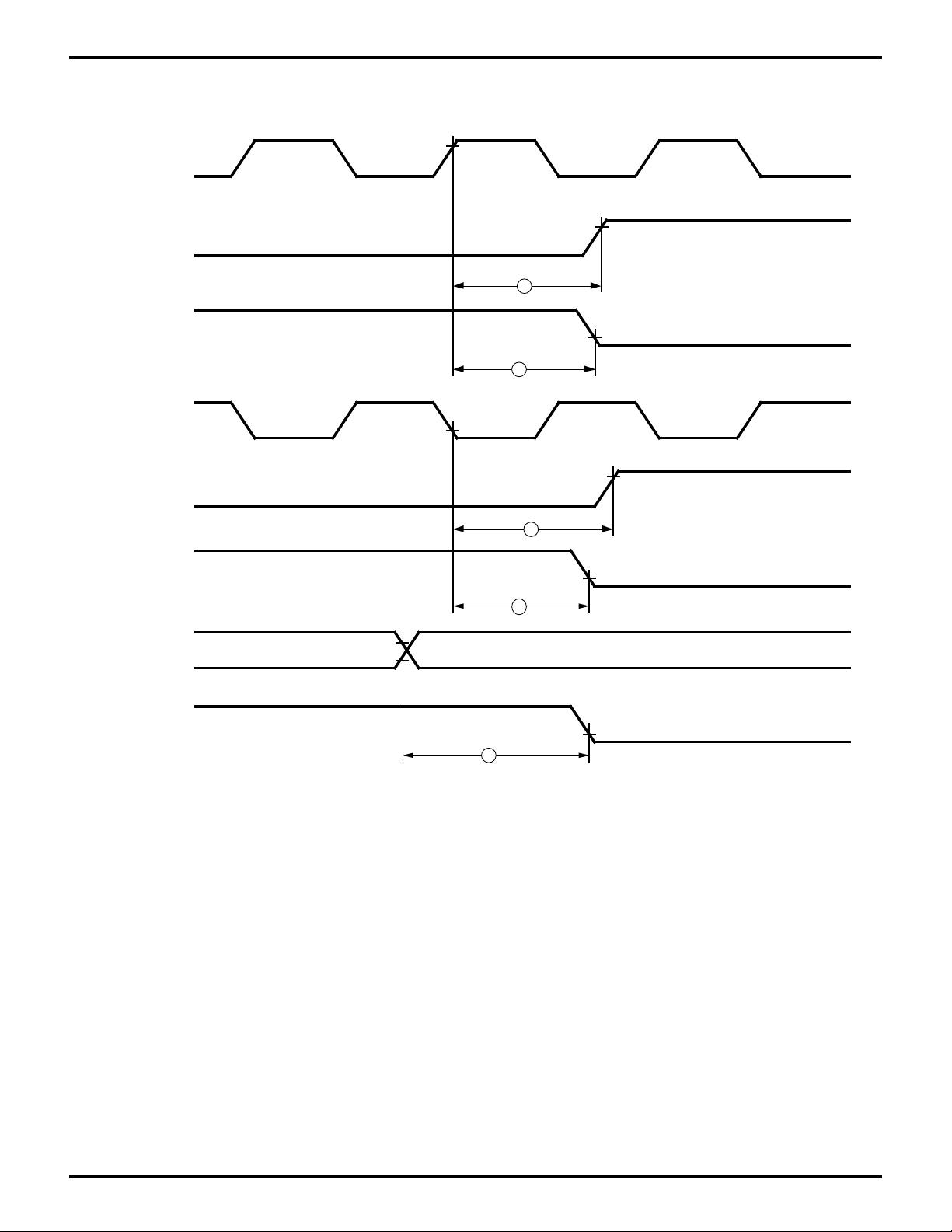
TIMING DIAGRAMS (Continued)
Ø
32
31
/INTI
33
/NMI
/M1 [1]
/IORQ [1]
PRELIMINARY
30
SMART PERIPHERAL CONTROLLES
Z80185/Z80195
16
15
/Data IN [1]
/MREQ [2]
/RFSH [2]
/BUSREQ
/BUSACK
Address
Data /MREQ,
/RD, /WR,
/IORQ
/HALT
39
35 35
34
43
Notes:
[1] During /INT0 acknowledge cycle
[2] During refresh cycle
4041 42
34
3736
[3]
[3] Output buffer is off at this point
[4] Refer to Table C, parameter 7
3838
44
DS971850301
Figure 5. CPU Timing
(/INT0 Acknowledge Cycle, Refresh Cycle, BUS RELEASE mode
HALT mode, SLEEP mode, SYSTEM STOP mode)
7
Zilog
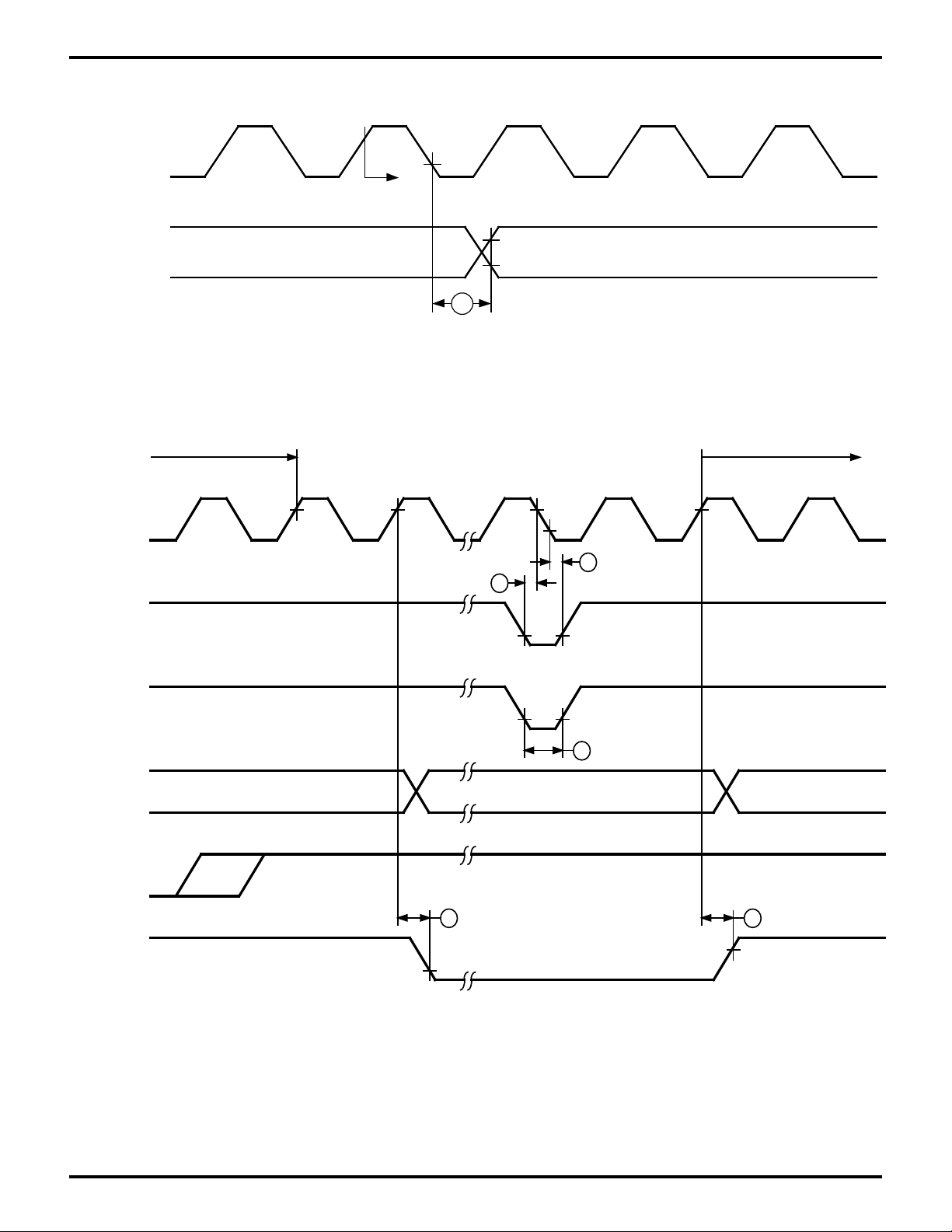
PRELIMINARY
SMART PERIPHERAL CONTROLLERS
Z80185/Z80195
Address
/IROQ
/RD
/WR
I/O Read Cycle
T1 T2 TW T3 T1
0
28
9
29
13
Figure 6. CPU Timing
CPU or DMA Read/Write Cycle
I/O Write Cycle
T2 TW T3
28
22
29
25
TOUT//DREQ
(At level
sense)
TOUT//DREQ
(At edge
sence)
ST
T1 T2 Tw T3 T1
Ø
45
[1]
46
45
[2]
45
[3]
17
18
[4]
DMA Control Signals
[1] tDRQS and tDRQH are specified for the rising edge of clock followed by T3.
[2] tDRQS and tDRQH are specified for the rising edge of clock.
[3] DMA cycle starts.
[4] CPU cycle starts.
Figure 7. DMA Control Signals
8
DS971850301
Zilog
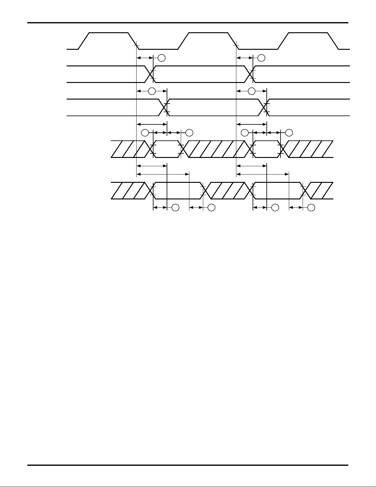
TIMING DIAGRAMS (Continued)
Ø
TOUT/DREQ
SLP Instruction Fetch Next Opcode Fetch
T3 T1 T2 TS TS T1 T2
PRELIMINARY
Timer Data
Reg = 0000H
47
Figure 8. Timer Output Timing
SMART PERIPHERAL CONTROLLES
Z80185/Z80195
Ø
/INTi
/NMI
A18-A0
/MREQ, /M1
/RD
/HALT
32
31
33
43 44
DS971850301
Figure 9. SLEEP Execution Cycle
9
Zilog
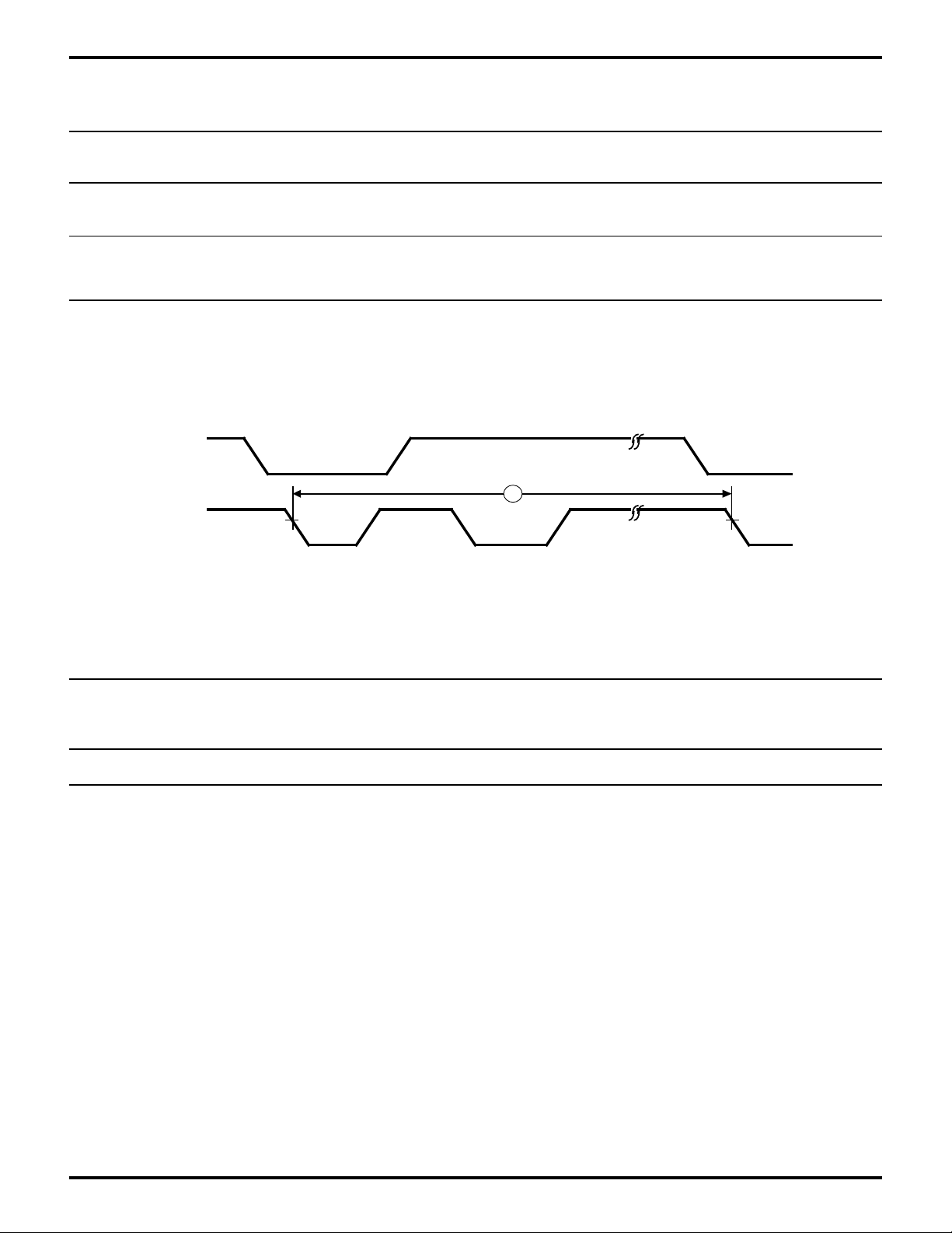
CSI/O Clock
Transmit Data
(Internal Clock)
Transmit Data
(External Clock)
Receive Data
(Internal Clock)
PRELIMINARY
57 57
5858
11 tcyc 11 tcyc
6059 6059
SMART PERIPHERAL CONTROLLERS
Z80185/Z80195
Receive Data
(External Clock)
11.5 tcyc
16.5 tcyc 16.5 tcyc
6261 61 62
11.5 tcyc
Figure 10. CSI/O Receive/Transmit Timing
10
DS971850301
Zilog
TIMING DIAGRAMS (Continued)
63
/MREQ
/RAMCS
/ROMCS
/IORQ
PRELIMINARY
SMART PERIPHERAL CONTROLLES
Z80185/Z80195
64
/IOCS
Figure 11. /ROMCS and /RAMCS Timing
51 52
EXTAL
VIL1
VIH1
VIH1
Figure 12. External Clock Rise Time
and Fall Time
VIL1
56
55
Figure 13. Input Rise and Fall Time
(Except EXTAL, /RESET)
DS971850301
11

Zilog
PRELIMINARY
SMART PERIPHERAL CONTROLLERS
Z80185/Z80195
AC CHARACTERISTICS
VDD = 5V ±10%, VSS = 0V, CL = 50 pF for outputs over
specified temperature range, unless otherwise noted.
Z80185 / Z80195 Z80185 / Z80195
(20 MHz) (33 MHz)
No. Symbol Parameter Min Max Min Max Units
1 tcy Clock Cycle Time 50 (DC) 33 (DC) ns
2 tCHW Clock “H” Pulse Width 15 10 ns
3 tCLW Clock “L” Pulse Width 15 10 ns
4 tcf Clock Fall Time 10 5 ns
5 tcr Clock Rise Time 10 5 ns
6 tAD PHI Rising to Address Valid 30 15 ns
7 tAS Address Valid to (MREQ Falling or IORQ Falling) 5 5 ns
8 tMED1 PHI Falling to MREQ Falling Delay 25 15 ns
9a tRDD1 PHI Falling to RD Falling Delay (IOC=1) 25 15 ns
9b tRDD1 PHI Rising to RD Falling Delay (IOC=0) 25 15 ns
10 tM1D1 PHI Rising to M1 Falling Delay 35 15 ns
11 tAH Address Hold Time from (MREQ, IOREQ, RD, WR) 5 5 ns
12 tMED2 PHI Falling to MREQ Rising Delay 25 15 ns
13 tRDD2 PHI Falling to RD Rising Delay 25 15 ns
14 tM1D2 PHI Rising to M1 Rising Delay 40 15 ns
15 tDRS Data Read Setup Time 10 5 ns
16 tDRH Data Read Hold Time 0 0 ns
17 tSTD1 PHI Falling to ST Falling Delay 30 15 ns
18 tSTD2 PHI Falling to ST Rising Delay 30 15 ns
19 tWS WAIT Setup Time to PHI Falling 15 10 ns
20 tWH WAIT Hold Time from PHI Falling 10 5 ns
21 tWDZ PHI Rising to Data Float Display 35 20 ns
22 tWRD1 PHI Rising to WR Falling Delay 25 15 ns
23 tWDD PHI Rising to Write Data Delay Time 25 15 ns
24 tWDS Write Data Setup Time to WR Falling 10 10 ns
25 tWRD2 PHI Falling to WR Rising Delay 25 15 ns
26 tWRP Write Pulse Width (Memory Write Cycle) 75 45 ns
26a tWRP Write Pulse Width (I/O Write Cycle) 130 70 ns
27 WDH Write Data Hold Time From (WR Rising) 10 5 ns
Notes:
Specifications 1 through 5 refer to an external clock input on EXTAL, and
provisionally to PHI clock output. When a quartz crystal is used with the
on-chip oscillator, a lower maximum frequency than that implied by spec.
#1 may apply.
12
DS971850301

Zilog
PRELIMINARY
SMART PERIPHERAL CONTROLLES
Z80185/Z80195
AC CHARACTERISTICS (Continued)
Z80185 / Z80195 Z80185 / Z80195
(20 MHz) (33 MHz)
No. Symbol Parameter Min Max Min Max Units
28a tIOD PHI Falling to IORQ Falling Delay IOC = 1) 25 15 ns
28b tIOD PHI Rising to IORQ Fallin g Delay (IOC =0) 25 15 ns
29 tIOD2 PHI Falling to IORQ Rising Delay 25 15 ns
30 tIOD3 M1 Falling to IORQ Falling Delay 100 80 ns
31 tINTS INT Setup Time to PHI Falling 20 15 ns
32 tINTH INT Hold Time from PHI Falling 10 10 ns
33 tNMIW NMI Pulse Width 35 25 ns
34 tBRS BUSREQ Setup Time to PHI Falling 10 10 ns
35 tBRH BUSREQ Hold Time from PHI Falling 10 10 ns
36 tBAD1 PHI Rising to BUSACK Falling Delay 25 15 ns
37 tBAD2 PHI Falling to BUSACK Rising Delay 25 15 ns
38 tBZD PHI Rising to Bus Floating Delay Time 40 30 ns
39 tMEWH MREQ Pulse Width (High) tcy –15 tcy –10 ns
40 tMEWL MREQ Pulse Width (Low) 2tcy –15 2tcy–10 ns
41 tRFD1 PHI Rising to RFSH Falling Delay 20 15 ns
42 tRFD2 PHI Rising to RFSH Rising Delay 20 15 ns
43 tHAD1 PHI Rising to HALT Falling Delay 15 15 ns
44 tHAD2 PHI Rising to HALT Rising Delay 15 15 ns
45 tDRQS DREQ Setup Time to PHI Rising 20 15 ns
46 tDRQH DREQ Hold Time from PHI Rising 20 15 ns
47 tTOD PHI Falling to Timer Output Delay 75 50 ns
48 tRES RESET Setup Time to PHI Falling 40 25 ns
49 tREH RESET Hold Time From PHI Falling 25 15 ns
50 tOSC Oscillator Stabilization Time 20 20 ms
51 tEXr External Clock Rise Time (EXTAL) 10 5 ns
52 tEXf External Clock Fall Time (EXTAL) 10 5 ns
53 tRr Reset Rise Time 50 50 ms
54 tRf Reset Fall Time 50 50 ms
55 tIr Input Rise Time (Except EXTAL, RESET) 50 50 ns
56 tIf Input Fall Time (Except EXTAL, RESET) 50 50 ns
57 tSTDI CSIO Transmit Data Delay Time 75 60 ns
(Internal Clock Operation)
58 tSTDE CSIO Transmit Data Delay Time 7.5 tcy +75 7.5 tcy +60 ns
(External Clock Operation)
59 tSRSI CSIO Receive Data Setup Time 75 60 ns
(Internal Clock Operation)
60 tSRHI CSIO Receive Data Hold Time 75 60 ns
(Internal Clock Operation)
61 tSRSE CSIO Receive Data Setup Time 75 60 ns
(External Clock Operation)
62 tSRHE CSIO Receive Data Hold Time 75 60 ns
(External Clock Operation)
63 tdCS MREQ Valid to RAMCS and ROMCS Valid Delay 15 15 ns
64 tdIOCS Rising IORQ Valid to Rising IOCS Valid Delay 10 10 ns
DS971850301
13
Zilog
PRELIMINARY
AC CHARACTERISTICS (Continued)
Read/Write External Bus Master Timing
SMART PERIPHERAL CONTROLLERS
Z80185/Z80195
Address
/IORQ
/RD
Data
/WR
Data
A7-A0
B7
B8
B1
B9
B2
B2
B6
B4
B5
Data Out
B3
Data In
Figure 14. Read/Write External Bus Master Timing
14
DS971850301
Zilog
PRELIMINARY
AC CHARACTERISTICS (Continued)
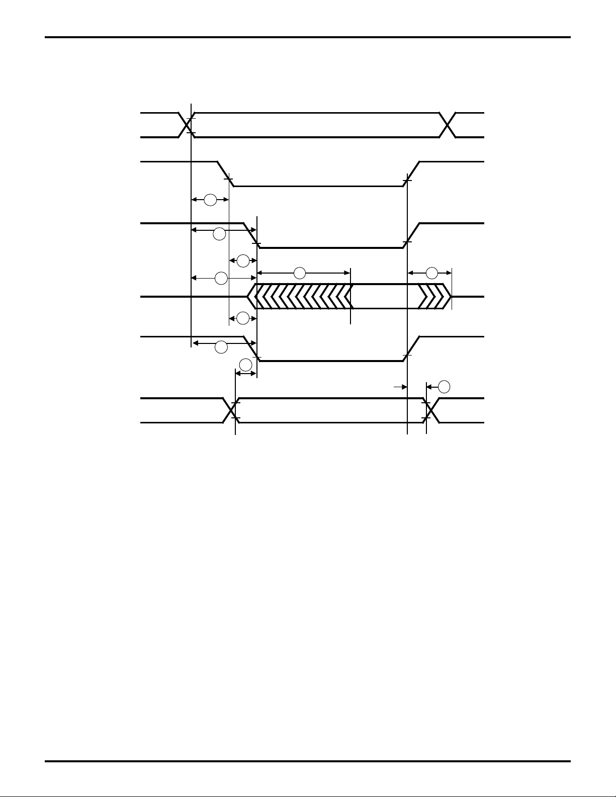
General-Purpose I/O Timing Port Timing
Parameters referenced in Figure 15 appear in the following
Tables. Note: Port 2 timing is different, even when Bidirectional Centronics feature is not in active use.
I/O Port Timing
(Output)
T1
T2
0
TW T3
T1 T2
TW
T3 T1 T2
SMART PERIPHERAL CONTROLLES
Z80185/Z80195
TW
T3
A0-A7
Port Data Dir. Reg. Addr. (Input) Port Data Reg. Addr. (Input) Port Data Reg. Addr. (Input)
B7
/IORQ
D0-D7
/WR
B2
Port
I/O Port Timing (Input)
A0-A7
/IORQ
(In) 'OO'H (Change Port To
Port Data Dir. Reg.
Output)
B6
Addr. (Input)
B7
Port Output Data 1
(In)
B3
B2
B6
B3
Port (Output)
A1
Port Data Reg.
Addr. (Input)
A1 A2
B7
Port Output Data 2 (In)
B6
B2
Port Output Data 1 (Out)
Port Data Reg.
D0-D7
/WR
/RD
Port
DS971850301
Previous
Output
(In) 'FF'H (Change
Port To Input)
Port Data 1 (Out)
B2
B4
Port Input Data
1 (In)
Figure 15. PORT Timing
Port Data
B2
B4
Port Input Data
2 (In)
2 Out
15

Zilog
PRELIMINARY
SMART PERIPHERAL CONTROLLERS
Z80185/Z80195
I/O Port Timing
Z80185 / Z80195 Z80185 / Z80195
(20 MHz) (33 MHz)
No. Symbol Parameter Min Max Min Max Units
A1 TdWR (PIA) Data Valid Delay from WR Rise 60 60 ns
External Bus Master Timing
Z80185 / Z80195 Z80185 / Z80195
(20 MHz) (33 MHz)
No. Symbol Parameter Min Max Min Max Units
B1 TsA(wf) Address Valid to WR or
(rf) RD Fall Time 40 40 ns
B2 TsIO(wf) IORQ Fall to WR or
(rf) RD Fall Time 20 20 ns
B3 Th Data Hold Time (from WR Rise) 5 5 ns
B4 TdRD(DO) RD Fall to Data Out Delay 35 35 ns
B5 TdRIr(DOz) RD,IORQ Rise to Data Float Time 5 5 ns
B6 TsDI(WRf) Data In to WR Fall Setup Time 20 20 ns
B7 TsA(IORQf) Address to IORQ Fall Setup Time 20 20 ns
B8 TsA(RDf) Address to RD Fall Setup Time 40 40 ns
B9 TsA(WRf) Address to WR Fall Setup Time 40 40 ns
16
DS971850301
Zilog
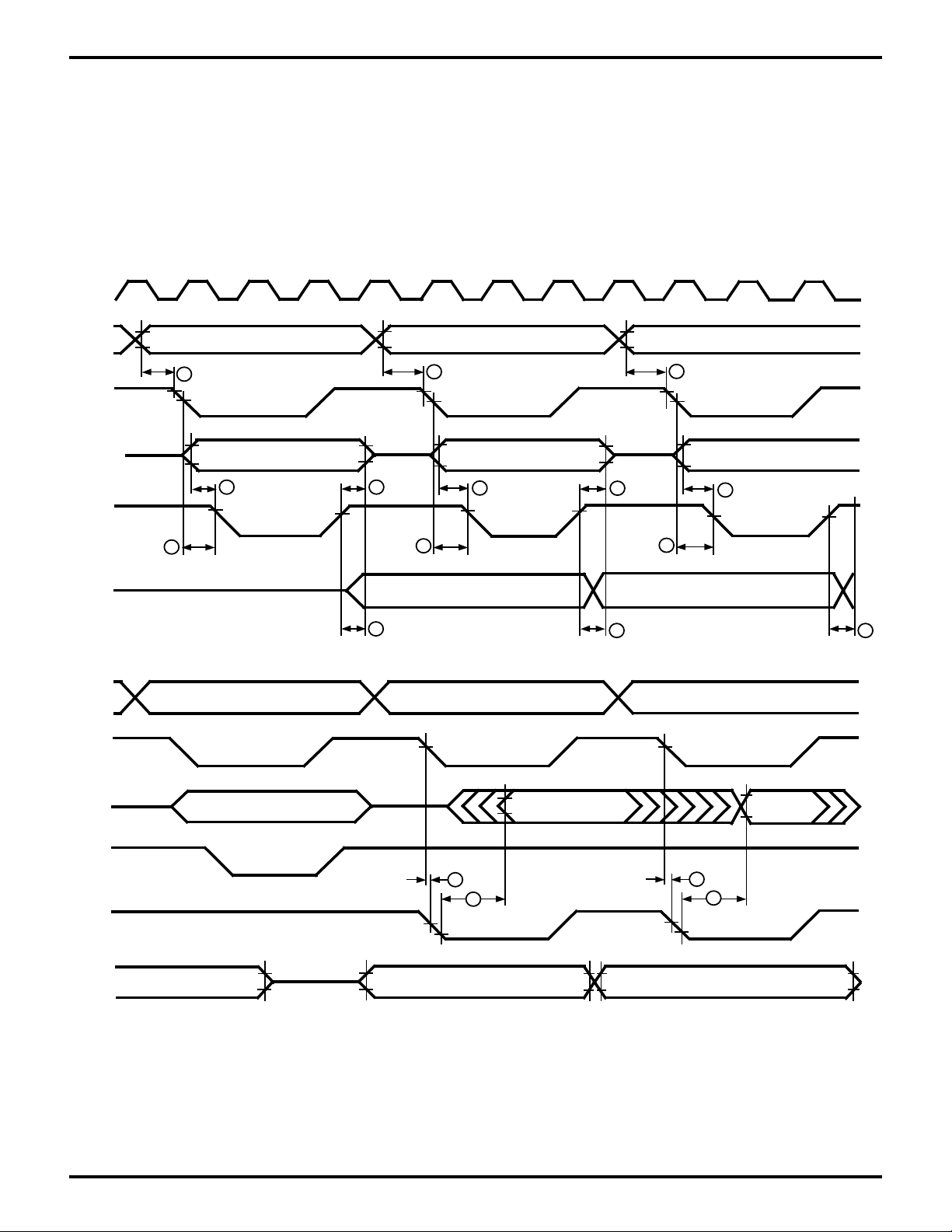
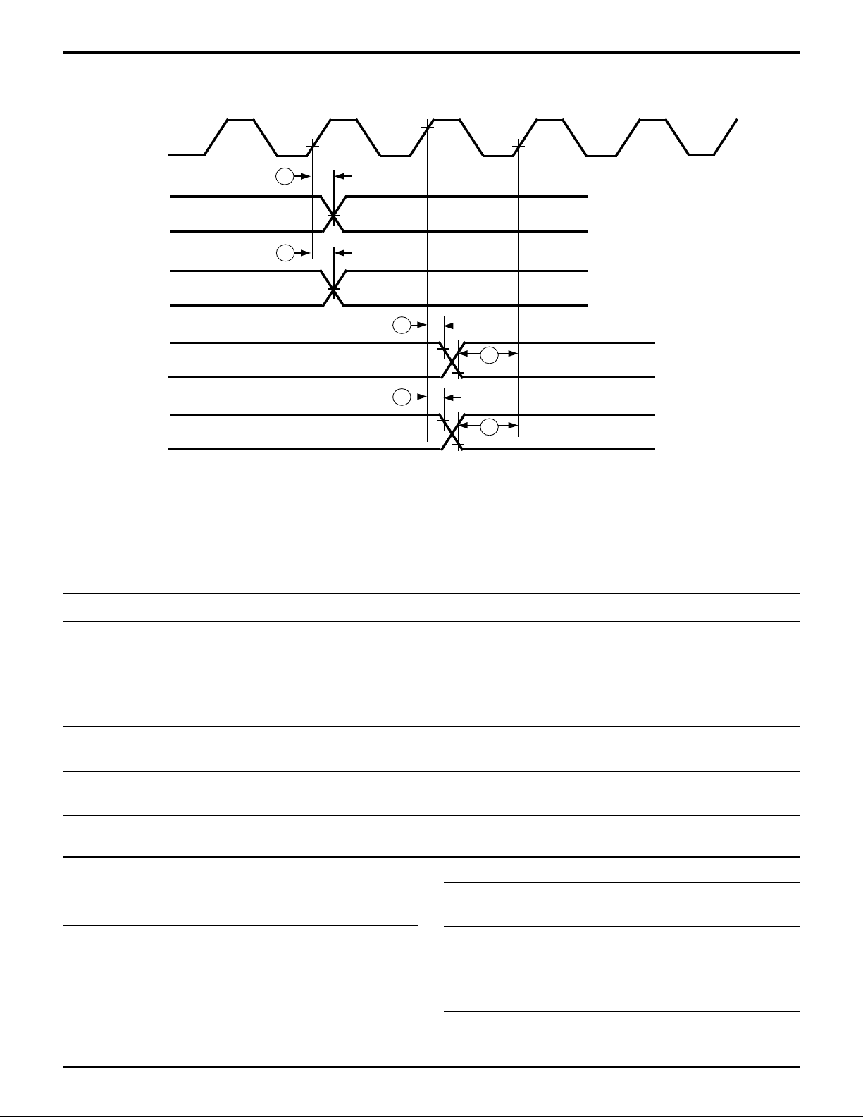
AC CHARACTERISTICS (Continued)
EMSCC Timing
Ø
/WR
/RD
Wait
PRELIMINARY
1
2
SMART PERIPHERAL CONTROLLES
Z80185/Z80195
/INT
EMSCC Timing Parameters
No. Symbol Parameter Min Max Unit
1 TdWR(W) /WR Fall to Wait Valid Delay 50 ns
2 TdRD(W) /RD Fall to Wait Valid Delay 50
6 TdPC(INT) Clock to /INT Valid Delay 160
6
Figure 16. EMSCC AC Parameters
20 MHz
DS971850301
17
Zilog
EMSCC General Timing Diagram
PCLK
Wait
3
/RTxC, /TRxC
Receive
4 5 6 7
RxD
10
/TRxC, /RTxC
Transmit
TxD
PRELIMINARY
2
11 12
SMART PERIPHERAL CONTROLLERS
Z80185/Z80195
/TRxC
Output
/RTxC
/TRxC
/CTS, /DCD
13
14 15
16
17
18 19
20
21 21
Figure 17. EMSCC General Timing Diagram
18
DS971850301

Zilog
PRELIMINARY
SMART PERIPHERAL CONTROLLES
AC CHARACTERISTICS (Continued)
EMSCC General Timing
20 MHz
No. Symbol Parameter Min Max Notes
2 TdPC(W) /PCLK to Wait Inactive 170
3 TsRxC(PC) /RxC to /PCLK Setup Time NA [1,4]
4 TsRxD(RxCr) RxD to /RxC Setup Time 0 [1]
5 ThRxD(RxCr) RxD to /RxC Hold Time 45 [1]
6 TsRxD(RxCf) RxD to /RxC Setup Time 0 [1,5]
7 ThRxD(RxCf) RxD to /RxC Hold Time 45 [1,5]
10 TsTxC(PC) /TxC to /PCLK Setup Time NA [2,4]
11 TdTxCf(TXD) /TxC to TxD Delay 70 [2]
12 TdTxCr(TXD) /TxC to TxD Delay 70 [2,5]
13 TdTxD(TRX) TxD to TRxC Delay 80 70
14 TwRTxh RTxC High Width 70 [6]
15 TwRTxI TRxC Low Width 70 [6]
16a TcRTx RTxC Cycle Time 200 [6,7]
16b TxRx(DPLL) DPLL Cycle Time Min 50 [7,8]
17 TcRTxx Crystal OSC. Period 61 1000 [3]
18 TwTRxh TRxC High Width 70 [6]
Z80185/Z80195
19 TwTRxl TRxC Low Width 70 [6]
20 TcTRx TRxC Cycle Time 200 [6,7]
21 TwExT DCD or CTS Pulse Width 60
Notes:
[1] RxC is /RTxC or /TRxC, whichever is supplying the receive clock.
[2] TxC is /TRxC or /RTxC, whichever is supplying the transmit clock.
[3] Both /RTxC and /SYNC have 30 pF capacitors to Ground connected to them.
[4] Synchronization of RxC to PCLK is eliminated in divide-by-four operation.
[5] Parameter applies only to FM encoding/decoding.
[6] Parameter applies only for transmitter and receiver; DPLL and baud
rate generator timing requirements are identical to case PCLK requirements.
[7] The maximum receive or transmit data rate is 1/4 PCLK.
[8] Applies to DPLL clock source only. Maximum data rate of 1/4 PCLK
still applies. DPLL clock should have a 50% duty cycle.
These AC parameter values are preliminary and subject to change without notice.
DS971850301
19
Zilog
EMSCC System Timing Diagram
/RTxC, /TRxC
Receive
/W/REQ
Wait
/INT
/RTxC, /TRxC
Transmit
PRELIMINARY
2
4
SMART PERIPHERAL CONTROLLERS
Z80185/Z80195
Wait
/INT
/CTS,
/DCD
/INT
6
8
10
Figure 18. EMSCC System Timing
20
DS971850301
Zilog
PRELIMINARY
SMART PERIPHERAL CONTROLLES
AC CHARACTERISTICS (Continued)
EMSCC System Timing
20 MHz
No. Symbol Parameter Min Max Notes
2 TdRxC(W) /RxC to /Wait Inactive 13 18 [1,2]
4 TdRxC(INT) /RxC to /INT Valid 15 22 [1,2]
6 TdTxC(W) /TxC to /Wait Inactive 8 17 [1,3]
8 TdTxC(INT) /TxC to /INT Valid 9 17 [1,3]
10 TdExT(INT) /DCD or /CTS to /INT Valid 3 9 [1]
Notes:
[1] Open-drain output, measured with open-drain test load.
[2] /RxC is /RTxC or /TRxC, whichever is supplying the receive clock.
Valid ESCC
Addr * IORQ
[3] /TxC is /TRxC or /RTxC, whichever is supplying the transmit clock.
[4] Units equal to TcPc
These AC parameter values are preliminary and subject to change
without notice.
Z80185/Z80195
1
/RD or
/WR
Figure 19. EMSCC External Bus Master Timing
External Bus Master Interface Timing (SCC Related Timing)
Z80185 / Z80195 Z80185 / Z80195
(20 MHz) (33 MHz)
No Symbol Parameter Min Max Min Max Unit Notes
1 TrC Valid Access Recovery Time 4TcC 4TcC ns [1]
Notes:
[1] Applies only between transactions involving the EMSCC.
These AC parameter values are preliminary and subject to change
without notice.
TCC = EMSCC Clock Period Time
DS971850301
21
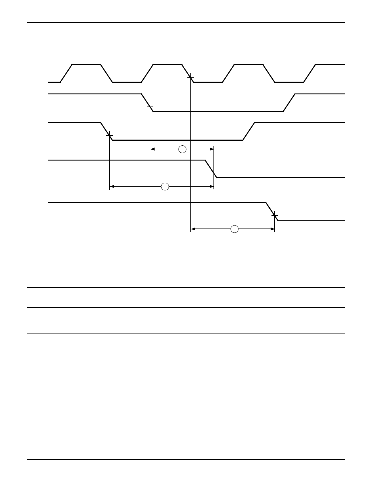
Zilog
AC CHARACTERISTICS (Continued)
φ
1
Port 2
Output
2
Control
Output
PRELIMINARY
4
SMART PERIPHERAL CONTROLLERS
Z80185/Z80195
Control
Input
6
Port 2
Input
3
5
Figure 20. P1284 Bidirectional Centronics Interface Timing
P1284 Bidirectional Centronics Interface Timing
No. Parameter Min Max Units Notes
1 CLK High to Port 2 Output 12 ns
2 CLK High to Control Output 12 ns [1]
3 Setup Time for Control Input to
CLK High for Guaranteed Recognition 10 ns [2]
4 Hold Time for Control Input from
CLK High for Guaranteed Recognition 5 ns [2]
5 Setup Time for Port 2 Inputs to
CLK High for Guaranteed Recognition 10 ns
6 Hold Time for Port 2 Inputs to
CLK High for Guaranteed Recognition 5 ns
Notes:
[1] Control Outputs
Peripheral Mode Host Mode
Busy/PtrBusy/PeriphAck nStrobe/HostClk
nAck/PtrClk/PeriphClk nAutoFd/HostBusy/HostAck
PError/AckDataReq/nAckReverse nSelectIn/P1284Active
nFault/nDataAvail/nPeriphRequest nInit/nReverseRequest
Select/Xflag
22
[2] Control Inputs
Host Mode Peripheral Mode
Busy/PtrBusy/PeriphAck nStrobe/HostClk
nAck/PtrClk/PeriphClk nAutoFd/HostBusy/HostAck
PError/AckDataReq/nAckReverse nSelectIn/P1284Active
nFault/nDataAvail/nPeriphRequest nInit/nReverseRequest
Select/Xflag
DS971850301

Zilog
PIN DESCRIPTIONS
PRELIMINARY
SMART PERIPHERAL CONTROLLES
Z80185/Z80195
Z80185 CPU Signals
A0-A19.
A0-A19 is a 20-bit address bus that provides the address
for memory data bus cycles up to 1 Mbyte, and I/O data
bus cycles up to 64 Kbytes. The address bus enters a High
impedance state during reset and external bus acknowledge cycles. This bus is an input when /BUSACK is Low.
No address lines are multiplexed with any other signals.
D0-D7.
D7 constitute an 8-bit bidirectional data bus, used to
transfer information to and from I/O and memory devices.
The data bus enters the High impedance state during reset
and external bus acknowledge cycles, as well as during
SLEEP and HALT states.
/RD.
cates that the CPU is ready to read data from memory or
an I/O device. The addressed I/O or memory device
should use this signal to gate data onto the CPU data bus.
This pin is tri-stated during bus acknowledge cycles.
/WR.
cates that the CPU data bus holds valid data to be stored
at the addressed I/O or memory location. This pin is tristated during bus acknowledge cycles.
/IORQ.
/IORQ indicates that the address bus contains a valid I/O
address for an I/O read or I/O write operation. /IORQ is also
generated, along with /M1, during the acknowledgment of
the /INT0 input signal to indicate that an interrupt response
vector can be placed onto the data bus. This pin is tristated during bus acknowledge cycles.
/M1.
with /MREQ, /M1 indicates that the current cycle is the
opcode fetch cycle of an instruction execution. Together
with /IORQ, /M1 indicates that the current cycle is for an
interrupt acknowledge. It is also used with the /HALT and
ST signal to indicate the status of the CPU machine cycle.
The processor can be configured so that this signal is
compatible with the /M1 signal of the Z80, or with the /LIR
signal of the Z64180. This pin is tri-stated during bus
acknowledge cycles.
/MREQ.
state). /MREQ indicates that the address bus holds a valid
address for a memory read or memory write operation. It is
included in the /RAMCS and /ROMCS signals, and because of this may not be needed in some applications. This
pin is tri-stated during bus acknowledge cycles.
Address Bus
Data Bus
Read
(input/output, active Low, tri-state). /RD indi-
Write
(input/output, active Low, tri-state). /WR indi-
I/O Request
Machine Cycle 1
Memory Request
(input/output, active High, tri-state).
(bidirectional, active High, tri-state). D0-
(input/output, active Low, tri-state).
(input/output, active Low). Together
(input/output, active Low, tri-
/WAIT. (input/open-drain output, active Low.) /WAIT indicates to the MPU that the addressed memory or I/O
devices are not ready for a data transfer. This input is used
to induce additional clock cycles into the current machine
cycle. External devices should also drive this pin in an
open-drain fashion. This results in a “wired OR” of the Wait
indications produced by external devices and those produced by the two separate Wait State generators in the
Z80185. If the wire-ORed input is sampled Low, then
additional wait states are inserted until the /WAIT input is
sampled High, at which time the cycle is completed.
/HALT.
is asserted after the CPU has executed either the HALT or
SLP instruction, and is waiting for either non-maskable or
maskable interrupt before operation can resume. It is also
used with the /M1 and /ST signals to indicate the status of
the CPU machine cycle. On exit of Halt/Sleep, the first
instruction fetch is delayed 16 clock cycles after the /HALT
pin goes High.
/BUSACK.
/BUSACK indicates to the requesting device that the MPU
address and data bus, as well as some control signals,
have entered their High impedance state.
/BUSREQ.
used by external devices (such as DMA controllers) to
request access to the system bus. This request has a
higher priority than /NMI and is always recognized at the
end of the current machine cycle. This signal stops the
CPU from executing further instructions and places the
address and data buses, and other control signals, into the
High impedance state.
/NMI.
gered). /NMI has a higher priority than /INT and is always
recognized at the end of an instruction, regardless of the
state of the interrupt enable flip-flops. This signal forces
CPU execution to continue at location 0066H.
/INT0.
output, active Low). This signal is generated by internal
and external I/O devices. External devices should also
drive this signal in an open-drain fashion. The CPU will
honor this request at the end of the current instruction cycle
as long as it is enabled, and the /NMI and /BUSREQ signals
are inactive. The CPU acknowledges this interrupt request
with an interrupt acknowledge cycle. During this cycle,
both the /M1 and /IORQ signals will become active.
Halt/Sleep Status
Bus Acknowledge
Bus Request
Non-Maskable Interrupt
(output, active Low). This output
(output, active Low).
(input, active Low). This input is
(input, negative edge trig-
Maskable Interrupt Request 0
(input/open-drain
DS971850301
23

Zilog
PRELIMINARY
SMART PERIPHERAL CONTROLLERS
Z80185/Z80195
/INT1, /INT2.
active Low). These signals are generated by external I/O
devices. The CPU will honor these requests at the end of
the current instruction cycle as long as the /NMI, /BUSREQ,
and /INT0 signals are inactive. The CPU will acknowledge
these interrupt requests with an interrupt acknowledge
cycle. Unlike the acknowledgment for /INT0 during this
cycle, neither the /M1 nor the /IORQ signals will become
active. These pins may be programmed to provide active
Low level, rising or falling edge interrupts. The level of the
external /INT1 and /INT2 pins may be read in the Interrupt
Edge Register.
/RFSH.
/MREQ active indicate that the current CPU machine cycle
and the contents of the address bus should be used for
refresh of dynamic memories. The low order eight bits of
the address bus (A7-A0) contain the refresh address.
Maskable Interrupt Requests 1 and 2
Refresh
(output, active Low, tri-state). /RFSH and
inputs,
Z80185 UART and CSIO Signals
CKA0/CKS.
output). An optional clock input or output for ASCI channel
0 or the Clocked Serial I/O Port.
/DCD0/CKA1.
Clock 1
for ASCI channel 0, or a clock input or output for ASCI
channel 1.
/RTS0/TxS.
Data
(output). A programmable modem control output for
ASCI channel 0, or the serial output from the CSIO channel.
/CTS0/RxS.
Data
(input). A Low-active modem control input for ASCI
channel 0, or the serial data input to the CSIO channel.
TXA0.
from ASCI channel 0.
RXA0.
ASCI channel 0.
RXA1.
ASCI channel 1.
Asynchronous Clock 0 or Serial Clock
(input/
Data Carrier Detect 0 or Asynchronous
(input/output). A Low-active modem status input
Request to Send 0 or Clocked Serial Transmit
Clear to Send 0 or Clocked Serial Receive
Transmit Data 0
Receive Data 0
Receive Data 1
(output). This output transmits data
(input). This input receives data for
(input). This input receives data for
Multiplexed Signal
TOUT//DREQ.
or output). This pin can be programmed to be either TOUT,
the High-active pulse output from PRT channel 1, or a Lowactive DMA Request input from an external peripheral.
Timer Out or External DMA Request
(input
Z80185 EMSCC Signals
TXD.
Transmit Data
data at standard TTL levels.
RXD.
Receive Data
at standard TTL levels.
/TRXC.
functions under program control. /TRXC may supply the
receive clock or the transmit clock in the input mode or
supply the output of the digital phase-locked loop, the
crystal oscillator, the baud rate generator, or the transmit
clock in the output mode.
/RTXC.
under program control. /RTXC may supply the receive
clock, the transmit clock, the clock for the baud rate
generator, or the clock for the digital phase-locked loop.
The receive clock may be 1, 16, 32, or 64 times the data
rate in asynchronous mode.
/CTS.
programmed as an “auto enable”, a Low on it enables the
EMSCC transmitter. If not programmed as an auto enable,
it can be used as a general-purpose input. This pin is
Schmitt-trigger buffered to accommodate slow rise-times.
The EMSCC detects transitions on this input and can
interrupt the processor on either logic level transition.
/DCD.
functions as an EMSCC receiver enable when programmed
as an “auto enable”; otherwise it can be used as a generalpurpose input pin. The pin is Schmitt-trigger buffered to
accommodate slow rise-times. The EMSCC detects transitions on this pin and can interrupt the processor on either
logic level transition.
Transmit/Receive Clock
Receive/Transmit Clock
Clear To Send
Data Carrier Detect
(output). This output transmits serial
(input). This input receives serial data
(input or output). This pin
(input). This pin functions
(input, active Low). If this pin is
(input, active Low). This pin
TXA1.
Transmit Data 1
from ASCI Channel 1.
24
(output). This output transmits data
DS971850301

Zilog
PIN DESCRIPTIONS (Continued)
PRELIMINARY
SMART PERIPHERAL CONTROLLES
Z80185/Z80195
EMSCC Signals
/RTS.
Request to Send
Request to Send (RTS) bit in Write Register 5 is set, the
/RTS signal goes Low. When the RTS bit is reset in the
Asynchronous mode and auto enables is on, the signal
goes High after the transmitter is empty. In Synchronous
mode, or in Asynchronous mode with auto enables off, the
/RTS pin strictly follows the state of the RTS bit. Thus the pin
can be used as a general-purpose output. In a special
“AppleTalk” mode on the Z80185, the pin is under hardware control.
/DTR.
Data Terminal Ready
“/DTR//REQ” functionality found in other SCC family members has been reconfigured internal to the EMSCC
megacell. The /DTR output is routed to this pin, while the
/REQ signal is routed to the DMA request multiplexing
logic as described in a later section on the EMSCC. This
pin follows the state of the DTR bit in WR5 of the EMSCC.
Note: The /W/REQ pin present on other SCC family members has its two possible functions reconfigured internal to
the EMSCC, and both functions are handled internally to
the Z80185. The Wait output of the EMSCC drives the
/WAIT signal in a wire-ORed fashion with other internal and
external peripherals. The /REQ component is routed to the
DMA request multiplexing logic as described in a later
section on the EMSCC.
(output, active Low). When the
(outputs, active Low). The
Z80185 Parallel Ports
PIA16-14.
These lines can be configured as inputs or outputs, or as
the “zero count/timeout” outputs of three of the four CTC
channels, on a bit-by-bit basis.
Port 1, Bits 6-4 or CTC ZC/TO2-0
(input/output).
PIA13-10.
output). These lines can be configured as inputs or outputs, or as the “clock/trigger” inputs of the four CTC
channels, on a bit-by-bit basis.
PIA27-20.
These lines can be configured as inputs or outputs on a bitby-bit basis when not used for Bidirectional Centronics
operation. However, when used for Bidirectional Centronics
operation, software and hardware controls the direction of
all eight as a unit.
Port 1, Bits 3-0 or CTC CLK/TRG3-0
Port 2, Data, or Bidirectional
(input/output).
(input/
Bidirectional Centronics Pins
nStrobe, nAutoFd, nSelectIn, nInit (input/outputs). These
are inputs when using P27-20 for the Peripheral side of a
Centronics controller, or outputs when using P27-20 for the
Host side of such an interface. In certain P1284 modes,
these pins assume other names as described in the
section on the Centronics P1284 controller. When not
using P27-20 for a Centronics controller, these pins can be
used as general-purpose inputs or outputs.
Busy, nAck, PError, nFault, Select (input/outputs). These
are outputs when using P27-20 for the Peripheral side of a
Centronics P1284 controller, or inputs when using P27-20
for the Host side of such an interface. In certain P1284
modes, these pins have other names as described in the
section on the Centronics P1284 controller. When not
using P27-20 for a Centronics P1284 controller, these pins
can be used as general-purpose outputs or inputs. These
pins always function in the opposite direction of the preceding group.
DS971850301
25

Zilog
PRELIMINARY
System Control Signals
ST.
Status
/M1 and /HALT output to indicate the nature of each CPU
machine cycle.
/RESET.
used for initializing the Z80185 and other devices in the
system. It must be kept Low for at least three system clock
cycles.
IEI.
Interrupt Enable Signal
with IEO to form a priority daisy-chain when there are
external interrupt-driven Z80-compatible peripherals.
IEO.
In an interrupt daisy-chain, IEO controls the interrupt of
external peripherals. IEO is active when IEI is 1 and the
CPU is not servicing an interrupt from the on-chip peripherals.
/IOCS. /IOCS decodes /IORQ, /M1, and as many address
lines as are necessary to ensure it is activated for an I/O
space access to any register in any block of eight registers
that does not contain any on-chip registers. Also included
in the decode is any programmed relocation of the “180
register set” in the ICR, and the “Decode High I/O” bit in the
System Configuration Register. If the “180 registers” aren’t
relocated, and “Decode High I/O” is 0, /IOCS is active from
address XX40 though XXD7, XXF8 through XXFF, and
NN00 through NN3F, where NN are non-zero. If the “180
registers” are not relocated and “Decode High I/O” is 1,
/IOCS is active from 0040 through 00D7, and 00F8 through
FFFF. /IOCS is active when an external master is in control
of the bus, as well as when the Z80185 processor has
control.
(output, active High). This signal is used with the
Reset Signal
Interrupt Enable Output Signal
(input, active Low). /RESET signal is
(input, active High). IEI is used
(output, active High).
SMART PERIPHERAL CONTROLLERS
/RAMCS.
signal is driven Low for memory accesses at addresses
that fall between the values programmed into the RAMLBR
and RAMUBR registers. It is active when an external
master has control of the bus, as well as when the Z80185
processor is in control.
/ROMCS.
output is driven Low for memory accesses between the top
of on-chip ROM (if on-chip ROM is enabled) and the value
programmed into the ROMBR register. It is active when an
external master has control of the bus, as well as when the
Z80185 processor is in control.
XTAL.
Crystal oscillator connection and should be left open if an
external clock is used instead of a crystal. The oscillator
input is not a TTL level (reference DC Characteristics
section).
EXTAL.
pin functions as a Crystal oscillator connection. An external clock can be input to the Z80185 on this pin when a
crystal is not used. This input is Schmitt-triggered.
PHI.
processor’s reference clock, and is provided for the use of
external logic. The frequency of this output may be equal
to, or one-half that of the crystal or input clock frequency,
depending on an internal register bit.
RAM Chip Select
ROM Chip Select
Crystal
(input, active High). This pin functions as the
External Clock/Crystal
System Clock
(output, active High). This output is the
(output, active Low). This
(output, active Low). This
(input, active High). This
Z80185/Z80195
26
DS971850301

Zilog
PRELIMINARY
Z80185 MPU FUNCTIONAL DESCRIPTION
SMART PERIPHERAL CONTROLLES
Z80185/Z80195
The Z80185 includes a Zilog Z8S180 MPU (Static Z80180
MPU). This allows software code compatibility with existing Z80/Z180 software code. The following is an overview
of the major functional units of the Z80185.
The MPU portion of the Z80185 is the Z8S180 core with
added features and modifications. The single-channel
EMSCC of the Z80185 is compatible with the Z85233
EMSCC and features additional enhancements for
LocalTalk and the demultiplexing of the /DTR//REQ and
/WT//REQ lines.
Architecture
The Z80185 combines a high performance CPU core with
a variety of system and I/O resources useful in a broad
range of applications. The CPU core consists of four
functional blocks:
■ Clock Generator
■ Bus State Controller (Dynamic Memory Refresh)
■ Memory Management Unit (MMU)
■ Central Processing Unit (CPU).
The integrated I/O resources make up the remaining
functional blocks:
■ Direct Memory Access (DMA control—two channels)
■ Asynchronous Serial Communications Controller
(ASCI, two channels)
■ Programmable Reload Timers (PRT, two channels)
■ Clocked Serial I/O
■ Channel (CSIO)
■ Enhanced Z85C30 (EMSCC)
■ Counter/Timer Channels (CTC)
■ Parallel I/O
■ Bidirectional Centronics Controller.
Clock Generator. This logic generates the system clock
from either an external crystal or clock input. The external
clock is divided by two, or one if programmed, and is
provided to both internal and external devices.
Bus State Controller. This logic performs all of the status
and bus control activity associated with both the CPU and
some on-chip peripherals. This includes wait state timing,
reset cycles, DRAM refresh, and DMA bus exchanges.
Interrupt Controller. This logic monitors and prioritizes
the variety of internal and external interrupts and traps to
provide the correct responses from the CPU. To maintain
compatibility with the Z80 CPU, three different interrupt
modes are supported.
Memory Management Unit. The MMU allows the user to
“map” the memory used by the CPU (logically only 64
Kbytes) into the 1 Mbyte addressing range supported by
the Z80185. The organization of the MMU object code
maintains compatibility with the Z80 CPU while offering
access to an extended memory space. This is accomplished by using an effective “common area-banked area”
scheme.
Central Processing Unit. The CPU is microcoded to
provide a core that is object-code compatible with the Z80
CPU. It also provides a superset of the Z80 instruction set,
including 8-bit multiply. This core has been modified to
allow many of the instructions to execute in fewer clock
cycles.
DMA Controller. The DMA controller provides high-speed
transfers between memory and I/O devices. Transfer operations supported are memory-to-memory, memory to or
from I/O, and I/O-to-I/O. Transfer modes supported are
request, burst, and cycle steal. DMA transfers can access
the full 1 Mbyte addressing range with a block length up to
64 Kbytes, and can cross over the 64 Kbytes boundaries.
DS971850301
27
Zilog
XTAL
EXTAL
PRELIMINARY
/WR
/RD
/RESET
/M1
/MREQ
/HALT
/IORQ
/BUSREQ
/WAIT
/RFSH
/BUSACK
SMART PERIPHERAL CONTROLLERS
Z80185/Z80195
/NMI
/INT0
/INT1
/INT2
TOUT/
/DREQ
/RTS0/TxS
/CTS0/RxS
CKA0/CKS
Timing &
Ø
Clock
Generator
16-Bit
Programmable
Reload Timers
(2)
Clocked
Serial I/O
Port
Address Bus (16-Bit)
MMU
Bus State Control
CPU
DMACs
(2)
Asynchronous
SCI
(Channel 0)
Data Bus (8-Bit)
Asynchronous
SCI
(Channel 1)
Interrupt
TOUT//DREQ
TxA0
CKA0/CKS
RxA0
/RTS0
/CTS0
/DCD0
TxA1
DCD0/CKA1
RxA1
28
A19-A0 D7-D0
Figure 21. Z8S180 MPU Block Diagram
DS971850301
Zilog
PRELIMINARY
Z80185 MPU FUNCTIONAL DESCRIPTION (Continued)
DMA Controller
SMART PERIPHERAL CONTROLLES
Z80185/Z80195
The two DMA channels of the Z80185 can transfer data to
or from the EMSCC channel, the parallel interface, the
async ports, or an external device. The I/O device encoding in SAR18-16 and DAR18-16 of the existing Z80180 is
modified as shown in Table 1.
Table 1. SAR18-16 and DAR18-16 I/O Device Encoding
SM1-0 SAR18-16 Source
11 000 ext (TOUT/DREQ)
11 001 ASCI0 Rx
11 010 ASCI1 Rx
11 011 EMSCC Rx
11 10X Reserved, do not program.
11 1X0
11 111 PIA27-20 in
Asynchronous Serial Communications
Interface (ASCI)
The ASCI logic provides two individual full-duplex UARTs.
Each channel includes a programmable baud rate generator and modem control signals. The ASCI channels can
also support a multiprocessor communications format. For
ASCI0, up to three modem control signals and one clock
signal can be pinned out, while ASCI1 has a data-only
interface.
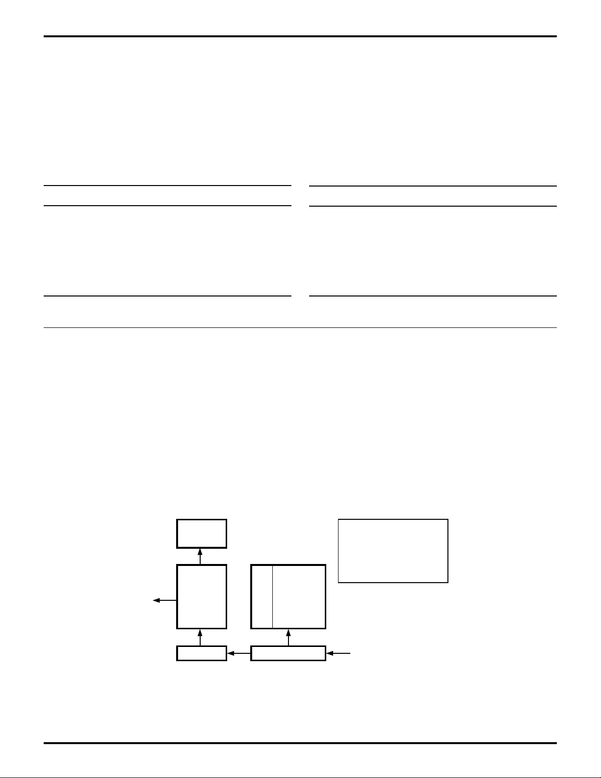
The receiver includes a 4-byte FIFO, plus a shift register as
shown in Figure 22.
DMA request signals between the various cells are handled
internally by the mechanisms described in this section,
and are not pinned-out, nor are the TEND termination
count outputs of the DMA channels.
DM1-0 DAR18-16 Destination
11 000 ext (TOUT/DREQ)
11 001 ASCI0 Tx
11 010 ASCI1 Tx
11 011 EMSCC Tx
11 10X Reserved, do not program.
11 1X0
11 111 PIA27-20 out
During Reset and in I/O Stop state, and for ASCI0 if /DCD0
is auto-enabled and is High, an ASCI is forced to the
following conditions:
■ FIFO Empty
■ All Error Bits Cleared (including those in the FIFO)
■ Receive Enable Cleared (cntla bit 6 = 0)
■ Transmit Enable Cleared (cntla bit 5 = 0).
If DCD is not auto-enabled, the /DCD pin has no effect on
the FIFOs or enable bits.
DS971850301
Overrun
Error
Error
Latches
4x4 Bit
Error
FIFO
P F O B
E E R K
Error Shift Register
MP
Bit
4-Byte
Data FIFO
Figure 22. ASCI Receiver
Notes:
PE = Parity Error
FE = Framing Error
OR = Overrun
BK = Break
MP = Multiprocessor Bit
RXA
29
 Loading...