

ZILOG Z8018110FEC Datasheet

Zilog
FEATURES
SMART ACCESS CONTROLLER SAC
Z80181
PRELIMINARY PRODUCT SPECIFICATION
Z80181
SMART ACCESS CONTROLLER (SAC
™
)
™
■ Z80180 Compatible MPU Core with 1 Channel of
Z85C30 SCC, Z80 CTC, Two 8-Bit General-Purpose
Parallel Ports, and Two Chip Select Signals.
■ High Speed Operation (10 MHz)
■ Low Power Consumption in Two Operating Modes:
- (TBD) mA Typ. (Run Mode)
- (TBD) mA Typ. (STOP Mode)
■ Wide Operational Voltage Range (5V ±10%)
■ TTL/CMOS Compatible
■ Clock Generator
■ One Channel of Z85C30 Serial Communication
Controller (SCC)
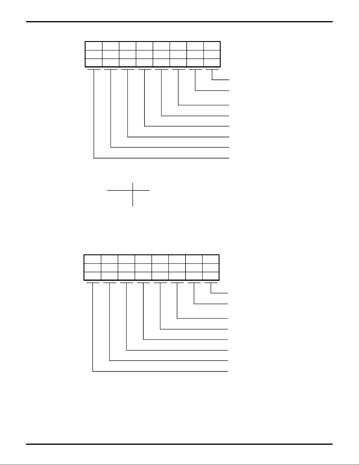
GENERAL DESCRIPTION
The Z80181 SAC™ Smart Access Controller (hereinafter,
referred to as Z181 SAC) is a sophisticated 8-bit CMOS
microprocessor that combines a Z180-compatible MPU
(Z181 MPU), one channel of Z85C30 Serial Communication Controller (SCC), a Z80 CTC, two 8-bit general-purpose parallel ports, and two chip select signals, into a
single 100-pin Quad Flat Pack (QFP) package (Figures 1
and 2). Created using Zilog's patented Superintegration
methodology of combining proprietary IC cores and cells,
this high-end intelligent peripheral controller is well-suited
for a broad range of intelligent communication control
applications such as terminals, printers, modems, and
slave communication processors for 8-, 16- and 32- bit
MPU based systems.
■ Z180 Compatible MPU Core Includes:
- Enhanced Z80 CPU Core
- Memory Management Unit (MMU) Enables Access
to 1MB of Memory
- Two Asynchronous Channels
- Two DMA Channels
- Two 16-Bit Timers
- Clocked Serial I/O Port
■ On-Board Z84C30 CTC
■ Two 8-Bit General-Purpose Parallel Ports
■ Memory Configurable RAM and ROM Chip Select Pins
■ 100-Pin QFP Package
Information on enhancement/cost reductions of existing
hardware using Z80/Z180 with Z8530/Z85C30 applications is also included in this product specification.
Notes:
All Signals with a preceding front slash, "/", are active Low, e.g.,
B//W (WORD is active Low); /B/W (BYTE is active Low, only).
™
Power connections follow conventional descriptions below:
Connection Circuit Device
Power V
Ground GND V
CC
V
DD
SS
DS971800500
2-1
Zilog
GENERAL DESCRIPTION (Continued)
SMART ACCESS CONTROLLER SAC
Z80181
™
D7-D0
Control
A19-A0
/ROMCS
/RAMCS
Compatible
A19-A12
Z80180
Core
(1 Channel)
Glue
Logic
Address
Decode
Logic
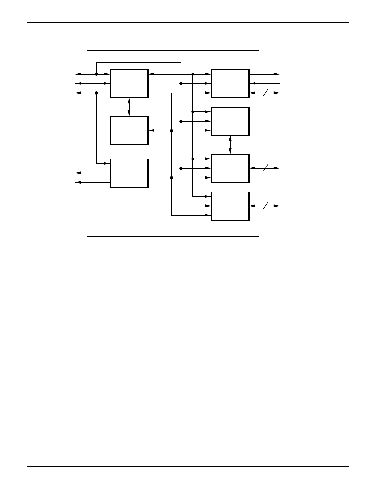
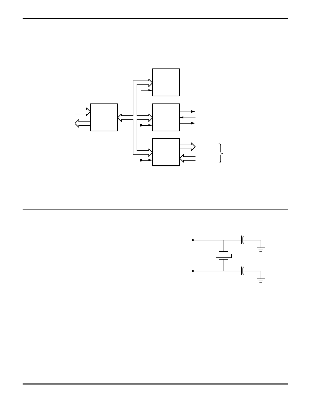
Z80181 = Z180 + SCC/2 + CTC + PIA
SCC
CTC
PIA1
PIA2
Tx Data
Rx Data
Modem/Control
8
Signals
Bit Programmable
8
Bi-directional I/O
or I/O Pins of CTC
Bit Programmable
Bi-directional I/O
8
Figure 1. Z80181 Functional Block Diagram
2-2
DS971800500
Zilog
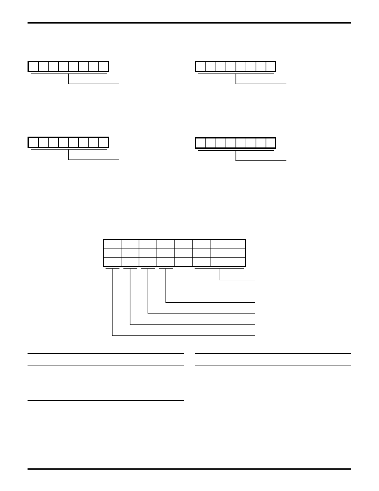
PIN DESCRIPTION
Z80181
SMART ACCESS CONTROLLER SAC
/WAIT
EXTAL
GND
/RESET
/BUSREQ
/BUSACK
/INTO
/NMI
XTAL
A17
PHI
/RD
/WR
/M1E/MREQ
/IORQ
/RFSH
+5V
/HALT
™
/INT1
/INT2
ST
A0
A1
A2
A3
A15
A4
A5
A6
A7
A8
A9
A10
A11
A12
GND
A13
A14
A16
D0
D1
D2
D3
D4
D5
D6
D7
/RAMCS
100
1
5
10
15
95
100-Pin QFP
20
25
30
90
Z80181
85
80
75
70
65
60
55
50454035
/TEND1
/DREQ1
CKS
RxS//CTS1
TxS
CKA1//TEND0
RxA1
TEST
TxA1
CKA0//DREQ0
RxA0
TxA0
/DCD0
/CTS0
/RTS0
A18/TOUT
A19
GND
IEI
/ROMCS
IEO
GND
/DCD
/CTS
/RTS
/DTR//REQ
TxD
/TRxC
RxD
/W//REQ
DS971800500
PIA10
+5V
PIA11
PIA12
PIA13
PAI14
PIA15
PIA16
PIA17
GND
PIA20
PIA21
PIA22
PIA23
Figure 2. 100-Pin QFP Pin Configuration
PIA24
PIA25
PIA26
PIA27
/RTxC
/SYNC
2-3

Zilog
SMART ACCESS CONTROLLER SAC
CPU SIGNALS
Pin Name Pin Number Input/Output, Tri-State Function
A19 - A0 4-17, 19-21, I/O, Active 1 Address Bus. A19 - A0 form a 20-bit address bus which
64, 65, 91 specifies I/O and memory addresses to be accessed.
During the refresh period, addresses for refreshing are
output. The address bus enters a high-impedance state
during Reset and external bus acknowledge cycles. The
bus is an input when the external bus master is accessing
the on-chip peripherals. Address line A18 is multiplexed
Z80181
with the output of PRT Channel 1 (T
output on Reset).
D0-D7 22-29 I/O, Active 1 8-Bit Bidirectional Data Bus. When the on-chip CPU is
accessing on-chip peripherals, these lines are outputs
and hold the data to/from the on-chip peripherals.
/RD 89 I/O, Active 0 Read Signal. CPU read signal for accepting data from
memory or I/O devices. When an external master is accessing the on-chip peripherals, it is an input signal.
/WR 88 I/O, Active 0 Write Signal. This signal is active when data to be stored
in a specified memory or peripheral device is on the MPU
data bus. When an external master is accessing the onchip peripherals, it is an input signal.
, selected as address
OUT
™
/MREQ 85 I/O, tri-state, Active 0 Memory Request Signal. When an effective address for
memory access is on the address bus, /MREQ is active.
This signal is analogous to the /ME signal of the Z64180.
/IORQ 84 I/O, tri-state, Active 0 I/O Request Signal. When addresses for I/O are on the
lower 8 bits (A7-A0) of the address bus in the I/O operation,
“0” is output. In addition, the /IORQ signal is output with the
/M1 signal during the interrupt acknowledge cycle to
inform peripheral devices that the interrupt response vector is on the data bus. This signal is analogous to the /IOE
signal of the Z64180.
/M1 87 I/O, tri-state, Active 0 Machine Cycle “1”. /MREQ and /M1 are active together
during the operation code fetch cycle. /M1 is output for
every opcode fetch when a two byte opcode is executed.
In the maskable interrupt acknowledge cycle, this signal is
output together with /IORQ. It is also used with
/HALT and ST signal to decode the status of the CPU
Machine cycle. This signal is analogous to the /LIR signal
of the Z64180.
/RFSH 83 Out, tri-state, Active 0 The Refresh Signal. When the dynamic memory
refresh address is on the low order 8-bits of the address
bus (A7 - A0), /RFSH is active along with the /MREQ signal.
This signal is analogous to the /REF signal of the Z64180.
2-4
DS971800500

Zilog
SMART ACCESS CONTROLLER SAC
Pin Name Pin Number Input/Output, Tri-State Function
/INT0 100 Wired-OR I/O, Active 0 Maskable Interrupt Request 0. Interrupt is generated by
peripheral devices. This signal is accepted if the interrupt
enable Flip-Flop (IFF) is set to “1”. Internally, the SCC and
CTC’s interrupt signals are connected to this line, and
require an external pull-up resistor.
/INT1, 1, 2, In, Active 0 Maskable Interrupt Request 1 and 2. This signal is
/INT2 generated by external peripheral devices. The CPU hon-
ors these requests at the end of current instruction cycle as
long as the /NMI, /BUSREQ and /INT0 signals are inactive.
The CPU will acknowledge these interrupt requests with an
interrupt acknowledge cycle. Unlike the acknowledgment
for /INT0, during this cycle, neither /M1 or /IORQ will
become active.
/NMI 99 In, Active 0 Non-Maskable Interrupt Request Signal. This interrupt
request has a higher priority than the maskable interrupt
request and does not rely upon the state of the interrupt
enable Flip-Flop (IFF).
/HALT 81 Out, tri-state, Active 0 Halt Signal. This signal is asserted after the CPU has
executed either the HALT or SLP instruction, and is waiting
for either non-maskable interrupt maskable interrupt before operation can resume. It is also used with the /M1 and
ST signals to decode the status of the CPU machine cycle.
Z80181
™
/BUSREQ 97 In, Active 0 BUS Request Signal. This signal is used by external
devices (such as a DMA controller) to request access to
the system bus. This request has higher priority than /NMI
and is always recognized at the end of the current machine
cycle. This signal will stop the CPU from executing further
instructions and place the address bus, data bus, /MREQ,
/IORQ, /RD and /WR signals into the high impedance state.
/BUSREQ is normally wired-OR and a pull-up resistor is
externally connected.
/BUSACK 96 Out, Active 0 Bus Acknowledge Signal. In response to /BUSREQ sig-
nal, /BUSACK informs a peripheral device that the address
bus, data bus, /MREQ, /IORQ, /RD and /WR signals have
been placed in the high impedance state.
/WAIT 95 Wired-OR I/O, Active 0 Wait Signal. /WAIT informs the CPU that the specified
memory or peripheral is not ready for a data transfer. As
long as /WAIT signal is active, the MPU is continuously kept
in the wait state. Internally, the /WAIT signal from the SCC
interface logic is connected to this line, and requires an
external pull-up resistor.
DS971800500
2-5

Zilog
SMART ACCESS CONTROLLER SAC
PERIPHERAL SIGNALS
Pin Name Pin Number Input/Output, Tri-State Function
RXA0, RXA1 70, 74 In, Active 1 ASCI Receive Data 0 and 1. These signals are the receive
data to the ASCI channels.
TXA0, TXA1 69, 72 Out, Active 1 ASCI Transmit Data 0 and 1. These signals are the
receive data to the ASCI channels. Transmit data changes
are with respect to the falling edge of the transmit clock.
/RTS0 66 Out, Active 0 Request to Send 0. This is a programmable modem
control signal for ASCI channel 0.
/DCD0 68 In, Active 0 Data Carrier Detect 0. This is a programmable modem
control signal for ASCI channel 0.
/CTS0 67 In, Active 0 Clear To Send 0. This is a programmable modem control
signal for ASCI channel 0.
/CTS1/RXS 77 In, Active 0 Clear To Send 0/Clocked Serial Receive Data. This is a
programmable modem control signal for ASCI channel 0.
Also, this signal becomes receive data for the CSIO
channel under program control. On power-on Reset, this
pin is set as RxS.
Z80181
™
CKA0//DREQ0 71 I/O, Active 1 Asynchronous Clock0/DMAC0 Request. This pin is the
transmit and receive clock for the Asynchronous channel
0. Also, under program control, this pin is used to request
a DMA transfer from DMA channel 0. DMA0 monitors this
input to determine when an external device is ready for a
read or write operation. On power-on Reset, this pin is
initialized as CKA0.
CKA1//TEND0 75 I/O, Active 1 Asynchronous Clock1/DMAC0 Transfer End. This pin is
the transmit and receive clock for the Asynchronous channel 1. Also, under program control, this pin becomes
/TEND0 and is asserted during the last write cycle of the
DMA0 operation and is used to indicate the end of the
block transfer. On power-on Reset, this pin initializes
as CKA1.
/TEND1 80 Out, Active 0 DMAC1 Transfer End. This pin is asserted during the last
write cycle of the DMA1 operation and is used to indicate
the end of the block transfer.
CKS 78 I/O, Active 1 CSIO Clock. This line is the clock for the CSIO channel.
TXS 76 Out, Active 1 CSI/O Tx Data. This line carries the transmit data from the
CSIO channel.
/DREQ1 79 In, Active 0 DMAC1 Request. This pin is used to request a DMA
transfer from DMA channel 1. DMA1 monitors this input to
determine when an external device is ready for a read or
write operation.
2-6
DS971800500

Zilog
SMART ACCESS CONTROLLER SAC
SCC SIGNALS
Pin Name Pin Number Input/Output, Tri-State Function
/W//REQ 51 Active 0 Wait/Request. Open-drain when programmed for a Wait
function, driven “1” or “0” when programming for a Request function. Used as /WAIT or /REQUEST depending
upon SCC programming. When programmed as /WAIT,
this signal is asserted to alert the CPU that addressed
memory or I/O devices are not ready and that the CPU
should wait. When programmed as /REQUEST, this signal
is asserted when a peripheral device associated with a
DMA port is ready to read/write data. After reset, this pin
becomes “/WAIT”.
/SYNC 50 I/O, Active 0 Synchronization. This pin can act either as input, output,
or part of the crystal oscillator circuit. In asynchronous
receive mode (crystal oscillator option not selected), this
pin is an input similar to /CTS and /DCD. In this mode,
transitions on this line affect the state of the Sync/Hunt
status bit in Read Register 0 but has no other function.
In external sync mode with crystal oscillator option not
selected, this line also acts as an input. In this mode,
/SYNC must be driven “0” two receive clock cycles after
the last bit in the synchronous character is received.
Character assembly begins on the rising edge of the
receive clock immediately preceding the activation
of /SYNC.
Z80181
™
In internal sync mode (Monosync and Bisync) with the
crystal oscillator option not selected, this line acts as
output and is active only during the part of the receive clock
cycle in which a synchronous character is recognized
(regardless of character boundaries). In SDLC mode, this
pin acts as an output and is valid on receipt of a flag.
RxD 52 In, Active 1 Receive Data. This input signal receives serial data at
standard TTL levels.
/RTxC 49 In, Active 0 Receive/Transmit Clock. This pin can be programmed in
several different modes of operation. /RTxC may supply
the receive clock, the transmit clock, the clock for the Baud
Rate Generator, or the clock for the Digital Phase-Locked
Loop. This pin can also be programmed for use with the
/SYNC pin as a crystal oscillator. The receive clocks can be
1, 16, 32, or 64 times the data transfer rate in Asynchronous
mode.
/TRxC 53 I/O, Active 0 Transmit/Receive Clock. This pin can be programmed in
several different modes of operation. /TRxC can supply the
receive clock or the transmit clock in the input mode. Also,
it can supply the output of the Digital Phase-Locked Loop,
the crystal oscillator, the Baud Rate Generator, or the
transmit clock in the output mode.
DS971800500
2-7

Zilog
SMART ACCESS CONTROLLER SAC
SCC SIGNALS (Continued)
Pin Name Pin Number Input/Output, Tri-State Function
TxD 54 Out, Active 1 Transmit Data. This Output signal transmits serial data at
standard TTL level.
/DTR//REQ 55 Out, Active 0 Data Terminal Ready/Request. This output follows the
state programmed into the DTR bit. It can also be used as
general-purpose output or as Request line for a DMA
controller.
/RTS 56 Out, Active 0 Request To Send. When the RTS bit in Write Register 5 is
set, the /RTS signal goes low. When the RTS bit is reset in
Asynchronous mode and auto enable is on, the signal
goes high after the transmitter is empty. In synchronous
mode or in Asynchronous mode, with Auto Enable off, the
/RTS pin follows the state of the RTS bit. This pin can be
used as a general-purpose output.
/CTS 57 In, Active 0 Clear To Send. If this pin is programmed as auto enable,
a “0” on the input enables the transmitter. If not programmed as Auto Enable, it may be used as a generalpurpose input. This input is Schmitt-trigger buffered to
accommodate inputs with slow rise times. The SCC detects pulses on this input and can interrupt the CPU on both
logic level transitions.
Z80181
™
/DCD 58 In, Active 0 Data Carrier Detect. This pin functions as receiver enable
if it is programmed for auto enable. Otherwise, it may be
used as a general-purpose input. This input is Schmitttrigger buffered to accommodate slow rise-time inputs.
The SCC detects pulses on this input and can interrupt the
CPU on both logic level transitions.
2-8
DS971800500

Zilog
SMART ACCESS CONTROLLER SAC
PIA/CTC SIGNALS
Pin Name Pin Number Input/Output, Tri-State Function
PIA17-PIA14 35-38 I/O Port 1 Data 7-Port 1 Data 4 or CTC ZC/TO3 - ZC/TO0.
These lines can be configured as inputs or outputs on a bit
-by-bit basis. Also, under program control, these bits
become Z80 CTC’s ZC/TO3 - ZC/TO0, and in either timer
or counter mode, pulses are output when the down counter
has reached zero. On reset, these signals function as
PIA17-14 and are inputs.
PIA13-PIA10 31-34 I/O Port 1 Data 3-Port 1 Data 0 or CTC CLK/TRG3-0. These
lines can be configured as inputs or outputs on a bit by bit
basis. Also, under program control, these bits become Z80
CTC’s CLK/TRG3-CLK/TRG0, and correspond to four
Counter/Timer Channels. In the counter mode, each active
edge causes the downcounter to decrement by one. In
timer mode, an active edge starts the timer. It is program
selectable whether the active edge is rising or falling. On
reset, these signals are set to PIA13-10 as inputs.
PIA27-20 41-48 I/O Port 2 Data. These lines are configured as inputs or
outputs on a bit-by-bit basis. On reset, they are inputs.
Z80181
™
DS971800500
2-9

Zilog
SMART ACCESS CONTROLLER SAC
SYSTEM CONTROL SIGNALS
Pin Name Pin Number Input/Output, Tri-State Function
ST 3 Out, Active 1 Status. This signal is used with the /M1 and /HALT output
to decode the status of the CPU machine cycle. Note that
the /M1 output is affected by the status of the M1E bit in the
OMCR register. The following table shows
the status while M1E=1.
ST /HALT /M1 Operation
0 1 0 CPU Operation
(1st Opcode fetch)
1 1 0 CPU Operation
(2nd and 3rd Opcode fetch)
1 1 1 CPU Operation
(MC other than Opcode fetch)
0 X 1 DMA operation
0 0 0 HALT mode
1 0 1 SLEEP mode
(Incl. System STOP mode)
Z80181
™
2-10
DS971800500

Zilog
SMART ACCESS CONTROLLER SAC
Pin Name Pin Number Input/Output, Tri-State Function
IEI 62 In, Active 1 Interrupt enable input signal. IEI is used with the IEO to
form a priority daisy chain when there is more than one
interrupt-driven peripheral.
IEO 60 Out, Active 1 The interrupt enable output signal. In the daisy-chain
interrupt control, IEO controls the interrupt of external
peripherals. IEO is active when IEI is “1” and the CPU is not
servicing an interrupt from the on-chip peripherals.
/ROMCS 61 Out, Active 0 ROM Chip select. Used to access ROM. Refer to “Func-
tional Description” on chip select signals for further explanation.
/RAMCS 30 Out, Active 0 RAM Chip Select. Used to access RAM. Refer to “Func-
tional Description” on chip select signals for further explanation.
/RESET 98 In, Active 0 Reset signal. /RESET signal is used for initializing the MPU
and other devices in the system. It must be kept in the
active state for a period of at least 3 system clock cycles.
Z80181
™
EXTAL 94 In, Active 1 Crystal oscillator connecting terminal. A parallel reso-
nant crystal is recommended. If an external clock source
is used as the input to the Z180 Clock Oscillator unit,
supply the clock into this terminal.
XTAL 93 Out Crystal oscillator connecting terminal.
PHI 90 Out, Active 1 System Clock. Single-phase clock output from Z181
MPU.
E 86 Out, Active 1 Enable Clock. Synchronous Machine cycle clock output
during a bus transaction.
TEST 73 Out Test pin. Used in the open state.
V
CC
V
SS
39, 82 Power Supply. +5 Volts
18, 40, 59, Power Supply. 0 Volts
63, 92
DS971800500
2-11
Zilog
FUNCTIONAL DESCRIPTION
SMART ACCESS CONTROLLER SAC
Z80181
™
Functionally, the on-chip Z181 MPU, SCC, and CTC are
the same as the discrete devices (Figure 1). Therefore,
refer to the Product Specification/Technical Manual of
/RD
/RESET
/WR
A18 /TOUT
TxS
RxS//CTS
CKS
XTAL
Ø
Timing
Generator
Programmable
Reload Timers
EXTAL
16-Bit
(2)
Clocked
Serial I/O
Port
each discrete product for a detailed description of each
individual unit. The following subsections describe each
individual functional unit of the SAC.
/M1
/IORQ
/MREQ
/WAIT
/HALT
/BUSREQ
/BUSACK
/RFSH
ST
/NMI
E
/INT0
/INT1
/INT2
Bus State Control Interrupt
CPU
/DREQ1
DMACs
/TEND
(2)
TxA0
CKA0 /DREQ0
Asynchronous
SCI
(Channel 0)
RxA0
/RTS0
/CTS0
/DCD0
Address Bus (16-Bit)
Data Bus (8-Bit)
MMU
A19-A0 D7-D0
Figure 3. Z181 MPU Block Diagram
Asynchronous
SCI
(Channel 1)
TxA1
CKA1 /TEND0
RxA1
2-12
DS971800500

Zilog
Z181 MPU
SMART ACCESS CONTROLLER SAC
Z80181
™
This unit provides all the capabilities and pins of the Zilog
Z180 MPU. Figure 3 shows the Z181 MPU block diagram.
This allows 100% software compatibility with existing Z180
(and Z80) software. Note that the on-chip I/O address
should not be relocated to the I/O address (from 0C0h to
0FFh) to avoid address conflicts. The following is an
overview of the major functional units of the Z181.
Z181 CPU
The Z181 CPU has 100% software compatibility with the
Z80 CPU. In addition, the Z181 CPU has the following
features:
Faster execution speed. The Z181 CPU is “fine tuned”
making execution speed, on average, 10% to 20% faster
than the Z80 CPU.
Enhanced DRAM Refresh Circuit. Z181 CPU’s DRAM
refresh circuit does periodic refresh and generates an
8-bit refresh address. It can be disabled or the refresh
period adjusted, through software control.
Enhanced Instruction Set. The Z181 CPU has seven
additional instructions to those of the Z80 CPU which
include the MLT (Multiply) instruction.
HALT and Low Power Modes of Operation. The Z181
CPU has HALT and low power modes of operation, which
are ideal for the applications requiring low power consumption like battery operated portable terminals.
System Stop Mode. When the Z181 SAC is in SYSTEM
STOP mode, it is only the Z181 MPU which is in STOP
mode. The on-chip CTC and SCC continue their normal
operation.
Instruction Set. The instruction set of the Z181 CPU is
identical to the Z180. For more details about each transaction, please refer to the Data Sheet/Technical Manual for
the Z180/Z80 CPU.
■ Maskable interrupt request operation
■ Trap and Non-Maskable interrupt request operation
■ HALT and low power modes of operation
■ Reset Operation
Memory Management Unit (MMU)
The Memory Management Unit (MMU) allows the user to
“map” the memory used by the CPU (64K bytes of logical
addressing space) into 1M bytes of physical addressing
space. The organization of the MMU allows object code
compatibility with the Z80 CPU while offering access to an
extended memory space. This is accomplished by using
an effective “common area-banked area” scheme.
DMA Controller
The Z181 MPU has two DMA controllers. Each DMA
controller provides high-speed data transfers between
memory and I/O devices. Transfer operations supported
are memory to memory, memory to/from I/O, and I/O to
I/O. Transfer modes supported are request, burst, and
cycle steal. The DMA can access the full 1M bytes addressing range with a block length up to 64K bytes and can
cross over 64K boundaries.
Asynchronous Serial Communication Interface
(ASCI)
This unit provides two individual full-duplex UARTs. Each
channel includes a programmable baud rate generator
and modem control signals. The ASCI channels also
support a multiprocessor communication format.
Programmable Reload Timer (PRT)
The Z181 MPU has two separate Programmable Reload
Timers, each containing a 16-bit counter (timer) and count
reload register. The time base for the counters is system
clock divided by 20. PRT channel 1 provides an optional
output to allow for waveform generation.
Z181 CPU Basic Operation
Z181 CPU’s basic operation consists of the following
events. These are identical to the Z180 MPU. For more
details about each operation, please refer to the Data
Sheet/Technical manual for the Z180.
■ Operation code fetch cycle
■ Memory Read/Write operation
■ Input/Output operation
■ Bus request/acknowledge operation
DS971800500
Clocked Serial I/O (CSI/O)
The CSI/O channel provides a half-duplex serial transmitter and receiver. This channel can be used for simple highspeed data connection to another CPU or MPU.
Programmable Wait State Generator
To ease interfacing with slow memory and I/O devices, the
Z181 MPU unit has a programmable wait state generator.
By programming the DMA/WAIT Control Register (DCNTL),
up to three wait states are automatically inserted in memory and I/O cycles. This unit also inserts wait states during
on-chip DMA transactions.
2-13
Zilog
FUNCTIONAL DESCRIPTION (Continued)
Baud Rate
Generator
Internal
Control
Logic
Channel
Registers
Internal BUS
10 X 19
Frame
Status
FIFO
Channel
Discrete
Control
& Status
SMART ACCESS CONTROLLER SAC
Z80181
} Serial Data
} Channel Clocks
/SYNC
/Wait
Modem, DMA,
or Other
Controls
™
Interrupt
Control
Lines
Interrupt
Control
Logic
Figure 4. SCC Block Diagram
Z85C30 Serial Communication Controller
Logic Unit
This logic unit provides the user with a multi-protocol serial
I/O channel that is completely compatible with the two
channel Z85C30 SCC with the following exceptions:
Their basic functions as serial-to-parallel and parallel-toserial converters can be programmed by the CPU for a
broad range of serial communications applications. This
logic unit is capable of supporting all common asynchronous and synchronous protocols (Monosync, Bisync, and
SDLC/HDLC, byte or bit oriented - Figure 4).
On the discrete version of the SCC (dual channel version),
there are two registers shared between channels A and B,
and two registers whose functions are different by channel. These are: WR2, WR9 (shared registers), and RR2 and
RR3 (different functionality).
Following are the differences in functionality:
■ RR2 - Returns Unmodified Vector or modified vector
depends on the status of “VIS” (Vector Include Status)
bit in WR9.
■ RR3 - Returns IP status (Ch.A side).
■ WR9 - Ch.B Software Reset command has no effect.
The PCLK for the SCC is connected to PHI (System clock),
the /INT signal is connected to /INT0 signal internally
(requires external pull-up resistor) and SCC is reset when
/RESET input becomes active. Interrupt from the SCC is
handled through Mode 2 interrupt. During the interrupt
acknowledge cycle, the on-chip SCC interface circuit
inserts two wait states automatically.
Z84C30 Counter/Timer Logic Unit
This logic unit provides the user with four individual 8-bit
Counter/Timer Channels that are compatible with the
Z84C30 CTC (Figure 5). The Counter/Timers are programmed by the CPU for a broad range of counting and
timing applications. Typical applications include event
counting, interrupt and interval counting, and serial baud
rate clock generation.
2-14
DS971800500
Zilog
SMART ACCESS CONTROLLER SAC
Z80181
™
Each of the Counter/Timer Channels, designated Channels 0-3, have an 8-bit prescaler (when used in timer
mode) and its own 8-bit counter to provide a wide range of
count resolution. Each of the channels have their own
Clock/Trigger input to quantify the counting process and
an output to indicate zero crossing/timeout conditions.
Data
Control
CPU
BUS
I/O
Internal Bus
These signals are multiplexed with the Parallel Interface
Adapter 1 (PIA1). With only one interrupt vector programmed into the logic unit, each channel can generate a
unique interrupt vector in response to the interrupt acknowledge cycle.
Internal
Control
Logic
4
4
/INT
IEI
IEO
ZC/TO
CLK/TRG
Mutiplexed
with PIA1
Interrupt
Logic
Counter/
Timer
Logic
/RESET
Figure 5. CTC Block Diagram
Parallel Interface Adapter (PIA)
The SAC has two 8-bit Parallel Interface Adapter (PIA)
Ports. The ports are referred to as PIA1 and PIA2. Each port
has two associated control registers; a Data Register and
a register to determine each bit’s direction (input or output). PIA1 is multiplexed with the CTC I/O pins. When the
CTC I/O feature is selected, the CTC I/O functions override
the PIA1 feature. Mode Selection is made through the
System Configuration Register (Address: EDh; Bit D0).
PIA1 has Schmitt-triggered inputs to have a better noise
margin. These ports are inputs after reset.
Clock Generator
The SAC uses the Z181 MPU’s on-chip clock generator to
supply system clock. The required clock is easily generated by connecting a crystal to the external terminals
(XTAL, EXTAL). The clock output runs at half the crystal
frequency. The system clock inputs of the SCC and the
CTC are internally connected to the PHI output of the Z181
MPU.
C1
XTAL
Crystal
Inputs
C2
EXTAL
Figure 6. Circuit Configuration For Crystal
DS971800500
2-15

Zilog
FUNCTIONAL DESCRIPTION (Continued)
SMART ACCESS CONTROLLER SAC
Z80181
™
Recommended characteristics of the crystal and the values for the capacitor are as follows (the values will change
with crystal frequency).
Type of crystal: Fundamental, parallel type crystal
(AT cut is recommended).
Frequency tolerance: Application dependent.
CL, Load capacitance: Approximately 22 pF
(acceptable range is 20-30 pF)
Rs, equivalent-series resistance: ≤ 30 Ohms
Drive level: 10 mW (for ≤ 10 MHz crystal) 5 mW
(for ≥ 10 MHz crystal)
CIN = C
= 15 ~ 22 pF.
OUT
Chip Select Signals
The SAC has two chip select (/RAMCS, /ROMCS) pins.
/ROMCS is the chip select signal for ROM and /RAMCS is
the chip select signal for RAM. The boundary value for
each chip select signal is 8 bits wide allowing all memory
accesses with addresses less than or equal to this boundary value. This causes assertion of the corresponding /CS
pin. These features are controlled through the RAM upper
boundary address register (I/O address EAh), RAM lower
boundary address register (I/O address EBh) and ROM
upper boundary address register (I/O address ECh).
These two signals are generated by decoding address
lines A19-A12. Note that glitches may be observed on the
/RAMCS and /ROMCS signals because the address decoding logic decodes only A19-A12, without any control
signals.
Bit D5 of the System Configuration Register allows the
option of disabling the /ROMCS signal. This feature is used
in systems which, for example, have a shadow RAM.
However, prior to disabling the /ROMCS signal, the ROMBR
and RAMLBR registers must be re-initialized from their
default values.
For more details, please refer to “Programming section”.
ROM Emulator Mode
To ease development, the SAC has a mode to support
“ROM emulator” development systems. In this mode, a
read data from on-chip registers (except Z181 MPU onchip registers) are available (data bus direction set to
output) to make data visible from the outside, so that a
ROM Emulator/Logic Analyzer can monitor internal transactions. Otherwise, a read from an internal transaction is
not available to the outside (data bus direction set to Hi-Z
status). Mode selection is made through the D1 bit in the
System Configuration Register (I/O Address: EDh).
Programming
The following subsections explain and define the parameters for I/O Address assignments, I/O Control Register
Addresses and all pertinent Timing parameters.
I/O Address Assignment
The SAC has 78 internal 8-bit registers to control on-chip
peripherals and features. Sixty-four registers out of 78
registers are occupied by the Z181 MPU control registers;
two for SCC control registers, four for PIA control registers,
four for the Counter/Timer, three for RAM/ROM configuration (memory address boundaries) and one for SAC’s
system control. The SAC’s I/O addresses are listed in
Table 1. These registers are assigned in the SAC’s I/O
addressing space and the I/O addresses are fully decoded from A7-A0 and have no image.
2-16
DS971800500

Zilog
PROGRAMMING (Continued)
SMART ACCESS CONTROLLER SAC
Z80181
™
Table 1. I/O Control Register Address
Address Register
00h Z181 MPU Control Registers
to 3Fh (Relocatable to 040h-07Fh, or 080h-0BFh)
E0h PIA1 Data Direction Register (P1DDR)
E1h PIA1 Data Port (P1DP)
E2h PIA2 Data Direction Register (P2DDR)
E3h PIA2 Data Register (P2DP)
E4h CTC Channel 0 Control Register (CTC0)
E5h CTC Channel 1 Control Register (CTC1)
E6h CTC Channel 2 Control Register (CTC2)
E7h CTC Channel 3 Control Register (CTC3)
E8h SCC Control Register (SCCCR)
E9h SCC Data Register (SCCDR)
EAh RAM Upper Boundary Address Register
(RAMUBR)
EBh RAM Lower Boundary Address Register
(RAMLBR)
ECh ROM Address Boundary Register (ROMBR)
EDh System Configuration Register (SCR)
EEh Reserved
EFh Reserved
Z181 MPU Control Registers
The I/O address for these registers can be relocated in 64
byte boundaries by programming of the I/O Control Register (Address xx111111b).
Do not relocate these registers to address from 0C0h since
this will cause an overlap of the Z180 registers and the 16
registers of the Z181 (address 0E0h to 0EFh).
Also, the OMCR register (Address: xx111101b) must be
programmed as 0x0xxxxxb (x: don’t care) as a part of the
initialization procedure. The M1E bit (Bit D7) of this register
must be programmed as 0 or the interrupt daisy chain is
corrupted. The /IOC bit (Bit D5) of this register is programmed as 0 so that the timing of the /RD and /IORQ
signals are compatible with Z80 peripherals.
For detailed information, refer to the Z180 Technical Manual.
DS971800500
2-17
Zilog
ASCI CHANNELS CONTROL REGISTERS
SMART ACCESS CONTROLLER SAC
Z80181
™
Bit
Upon RESET
R/W
CNTLA0
MPE
R/W0R/W0R/W1R/WxR/W0R/W0R/W0R/W
RE TE /RTS0
0
MPBR/
MOD2 MOD1 MOD0
EFR
0 0 0 Start + 7-Bit Data + 1 Stop
0 0 1 Start + 7-Bit Data + 2 Stop
0 1 0 Start + 7-Bit Data + Parity + 1 Stop
0 1 1 Start + 7-Bit Data + Parity + 2 Stop
1 0 0 Start + 8-Bit Data + 1 Stop
1 0 1 Start + 8-Bit Data + 2 Stop
1 1 0 Start + 8-Bit Data + Parity + 1 Stop
1 1 1 Start + 8-Bit Data + Parity + 2 Stop
Addr 00h
Figure 7. ASCI Control Register A (Ch. 0)
MODE Selection
Read - Multiprocessor Bit Receive
Write - Error Flag Reset
Request To Send
Transmit Enable
Receive Enable
Multiprocessor Enable
Bit
Upon RESET
R/W
CNTLA1
MPE RE TE
0
R/W0R/W0R/W1R/WxR/W0R/W0R/W0R/W
CKA1D
MPBR/
MOD2 MOD1 MOD0
EFR
0 0 0 Start + 7-Bit Data + 1 Stop
0 0 1 Start + 7-Bit Data + 2 Stop
0 1 0 Start + 7-Bit Data + Parity + 1 Stop
0 1 1 Start + 7-Bit Data + Parity + 2 Stop
1 0 0 Start + 8-Bit Data + 1 Stop
1 0 1 Start + 8-Bit Data + 2 Stop
1 1 0 Start + 8-Bit Data + Parity + 1 Stop
1 1 1 Start + 8-Bit Data + Parity + 2 Stop
Addr 01h
Figure 8. ASCI Control Register A (Ch. 1)
MODE Selection
Read - Multiprocessor Bit Receive
Write - Error Flag Reset
CKA1 Disable
Transmit Enable
Receive Enable
Multiprocessor Enable
2-18
DS971800500
Zilog
SMART ACCESS CONTROLLER SAC
Z80181
™
Addr 02h
Clock Source and Speed Select
Divide Ratio
Parity Even or Odd
Clear To Send/Prescale
Multiprocessor
Multiprocessor Bit Transmit
Bit
Upon Reset
CNTLB0
MPBT MP
Invalid
R/W0R/W†R/W0R/W0R/W1R/W1R/W1R/WR/W
† /CTS - Depending on the condition of /CTS pin.
PS - Cleared to 0.
/CTS/
PS
SS2 SS1 SS0
DRPE0
General PS = 0 PS = 1
Divide Ratio (Divide Ratio = 10) (Divide Ratio = 30)
SS, 2, 1, 0 DR = 0 (x16) DR = 1 (x64) DR = 0 (x16) DR = 1 (x64)
000 Ø ÷ 160 Ø ÷ 640 Ø ÷ 480 Ø ÷ 1920
001 Ø ÷ 320 Ø ÷ 1280 Ø ÷ 960 Ø ÷ 3840
010 Ø ÷ 640 Ø ÷ 2580 Ø ÷ 1920 Ø ÷ 7680
011 Ø ÷ 1280 Ø ÷ 5120 Ø ÷ 3840 Ø ÷ 15360
100 Ø ÷ 2560 Ø ÷ 10240 Ø ÷ 7680 Ø ÷ 30720
101 Ø ÷ 5120 Ø ÷ 20480 Ø ÷ 15360 Ø ÷ 61440
110 Ø ÷ 10240 Ø ÷ 40960 Ø ÷ 30720 Ø ÷ 122880
111 External Clock (Frequency < Ø ÷ 40)
Figure 9. ASCI Control Register B (Ch. 0)
DS971800500
2-19
Zilog
ASCI CHANNELS CONTROL REGISTERS (Continued)
SMART ACCESS CONTROLLER SAC
Z80181
™
Bit
Upon Reset
CNTLB1
MPBT MP
Invalid
R/W0R/W0R/W0R/W0R/W1R/W1R/W1R/WR/W
/CTS/
PS
SS2 SS1 SS0
DRPE0
Addr 03h
Clock Source and Speed Select
Divide Ratio
Parity Even or Odd
Read - Status of /CTS pin
Write - Select PS
Multiprocessor
Multiprocessor Bit Transmit
General PS = 0 PS = 1
Divide Ratio (Divide Ratio = 10) (Divide Ratio = 30)
SS, 2, 1, 0 DR = 0 (x16) DR = 1 (x64) DR = 0 (x16) DR = 1 (x64)
000 Ø ÷ 160 Ø ÷ 640 Ø ÷ 480 Ø ÷ 1920
001 Ø ÷ 320 Ø ÷ 1280 Ø ÷ 960 Ø ÷ 3840
010 Ø ÷ 640 Ø ÷ 2580 Ø ÷ 1920 Ø ÷ 7680
011 Ø ÷ 1280 Ø ÷ 5120 Ø ÷ 3840 Ø ÷ 15360
100 Ø ÷ 2560 Ø ÷ 10240 Ø ÷ 7680 Ø ÷ 30720
101 Ø ÷ 5120 Ø ÷ 20480 Ø ÷ 15360 Ø ÷ 61440
110 Ø ÷ 10240 Ø ÷ 40960 Ø ÷ 30720 Ø ÷ 122880
111 External Clock (Frequency < Ø ÷ 40)
Figure 10. ASCI Control Register B (Ch. 1)
2-20
DS971800500
Zilog
SMART ACCESS CONTROLLER SAC
Z80181
™
Bit
Upon Reset
STAT0
RDRF OVRN /DCD0TDRE TIE
0
R
† /DCD
†† /CTS
L 1
H 0
PE
0
0
R
R
0
- Depending on the condition of /DCD0 Pin.
0
Pin TDRE
RIEFE
0
R0R/W R
†
Addr 04h
††
R0R/WR/W
Transmit Interrupt Enable
Transmit Data Register
Empty
Data Carrier Detect
Receive Interrupt Enable
Framing Error
Parity Error
Over Run Error
Receive Data Register Full
Bit
Upon Reset
STAT1
RDRF OVRN
0
R
Figure 11. ASCI Status Register
CTS1E
PE
0
0
R
R
RIEFE
0
R0R/W R/W1R0R/WR/W
TDRE TIE
0
Figure 12. ASCI Status Register (Ch. 1)
Addr 05h
Transmit Interrupt Enable
Transmit Data Register
Empty
/CTS1 Enable
Receive Interrupt Enable
Framing Error
Parity Error
Over Run Error
Receive Data Register Full
DS971800500
2-21
Zilog
ASCI CHANNELS CONTROL REGISTERS (Continued)
SMART ACCESS CONTROLLER SAC
Z80181
™
TDR0
Write Only Addr 06h
76543210
Transmit Data
Figure 13. ASCI Transmit Data Register (Ch. 0)
TDR1
Write Only
76543210
Addr 07h
Transmit Data
Figure 14. ASCI Transmit Data Register (Ch. 1)
CSI/O Registers
TSR0
Read Only
xxxxxxxx
Addr 08h
Received Data
Figure 15. ASCI Receive Data Register (Ch. 0)
TSR1
Read Only
xxxxxxxx
Addr 09h
Received Data
Figure 16. ASCI Receive Data Register (Ch. 1)
CNTR
EF EIE SS2 SS1 SS0
Bit
Upon Reset
0
R0R/W0R/W0R/W
SS2, 1, 0 Baud Rate
000 Ø ÷ 20
001 Ø ÷ 40
010 Ø ÷ 80
011 Ø ÷ 100
RE
Addr 0Ah
-TE
11
R/W1R/W1R/WR/W
Speed Select
Transmit Enable
Receive Enable
End Interrupt Enable
End Flag
SS2, 1, 0 Baud Rate
100 Ø ÷ 320
101 Ø ÷ 640
110 Ø ÷ 1280
111 External Clock
(Frequency < Ø ÷ 20)
2-22
Figure 17. CSI/O Control Register
DS971800500
Zilog
TIMER REGISTERS
Timer Data Registers
TRDR
Read/Write
76543210
Addr 0Bh
Read - Received Data
Write - Transmit Data
Figure 18. CSI/O Transmit/Receive Data Register
SMART ACCESS CONTROLLER SAC
Z80181
™
TMDR0L
Read/Write
76543210
Figure 19. Timer 0 Data Register L
TMDR1L
Read/Write
76543210
Figure 20. Timer 1 Data Register L
Timer Reload Registers
Addr 0Ch
Addr 14h
TMDR0H
Read/Write
15 14 13 12 11 10 9 8
When Read, read Data Register L
before reading Data Register H.
Addr 0Dh
Figure 21. Timer 0 Data Register H
TMDR1H
Read/Write
15 14 13 12 11 10 9 8
When Read, read Data Register L
before reading Data Register H.
Addr 15h
Figure 22. Timer 1 Data Register H
Figure 23. Timer 0 Reload Register L
DS971800500
RLDR0L
Read/Write
76543210
Addr 0Eh
RLDR1L
Read/Write
76543210
Addr 16h
Figure 24. Timer 1 Reload Register L
2-23
 Loading...