


1
P
RELIMINARY
P
RODUCT
S
PECIFICATION
FEATURES
■
Code Compatible with Zilog Z80
■
Extended Instructions
Two Chain-Linked DMA Channels
■
■
Low Power-Down Modes
■
On-Chip Interrupt Controllers
■
Three On-Chip Wait-State Generators
■
On-Chip Oscillator/Generator
■
Expanded MMU Addressing (up to 1 MB)
■
Clocked Serial I/O Port
®
CPU
Z80180/Z8S180/
Z8L180 SL1919
E
NHANCED
■
Two 16-Bit Counter/Timers
■
Two Enhanced UARTs (up to 512 Kbps)
Clock Speeds: 6, 8, 10, 20, 33 MHz
■
■
Operating Range: 5V (3.3V@ 20 MHz)
■
Operating Temperature Range: 0
■
■
°
-40
C to +85
Three Packaging Styles
– 68-Pin PLCC
– 64-Pin DIP
– 80-Pin QFP
Z180 M
°
C Extended Temperature Range
ICROPROCESSOR
°
C to +70
1
°
C
GENERAL DESCRIPTION
The enhanced Z80180/Z8S180/Z8L180
proves on the previous Z80180 models while still providing
full backward compatibility with existing Zilog Z80 devices.
The Z80180/Z8S180/Z8L180 now offers faster execution
speeds, power saving modes, and EMI noise reduction.
This enhanced Z180 design also incorporates additional
feature enhancements to the ASCIs, DMAs, and I
STANDBY Mode power consumption. With the addition of
“ESCC-like” Baud Rate Generators (BRGs), the two ASCIs
now have the flexibility and capability to transfer data asynchronously at rates of up to 512 Kbps. In addition, the ASCI
receiver has added a 4-byte First In First Out (FIFO) which
can be used to buffer incoming data to reduce the incidence of overrun errors. The DMAs have been modified to
allow for a “chain-linking” of the two DMA channels when
set to take their DMA requests from the same peripherals
device. This feature allows for non-stop DMA operation between the two DMA channels, reducing the amount of CPU
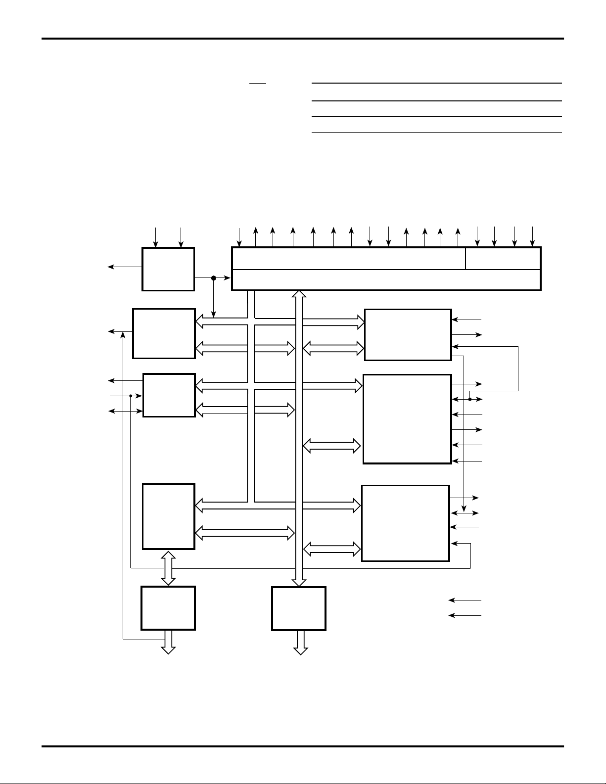
intervention (Figure 1).
™
significantly im-
cc
Not only does the Z80180/Z8S180/Z8L180 consume less
power during normal operations than the previous model,
it has also been designed with three modes intended to further reduce the power consumption. Zilog reduced I
er consumption during STANDBY Mode to a minimum of
10 µ A by stopping the external oscillators and internal
clock. The SLEEP mode reduces power by placing the
CPU into a “stopped” state, thereby consuming less current while the on-chip I/O device is still operating. The
SYSTEM STOP mode places both the CPU and the onchip peripherals into a “stopped” mode, thereby reducing
power consumption even further.
A new clock doubler feature has been implemented in the
Z80180/Z8S180/Z8L180 device that allows the programmer to double the internal clock from that of the external
clock. This provides a systems cost savings by allowing
the use of lower cost, lower frequency crystals instead of
the higher cost, and higher speed oscillators.
The Enhanced Z180 is housed in 80-pin QFP, 68-pin
PLCC, and 64-pin DIP packages.
cc
pow-
DS971800401
P R E L I M I N A R Y
1-1
Z80180/Z8S180/Z8L180
Enhanced Z180 Microprocessor Zilog
Notes: All Signals with a preceding front slash, “/” are ac-
tive Low, for example, B//W (WORD is active Low); /B/W
(BYTE is active Low, only). Alternatively, an overslash
may be used to signify active Low, for example WR
EXTAL
A18/TOUT
XTAL
Ø
Timing
Generator
16-bit
Programmable
Reload Timers
(2)
/RESET
/RD
/WR
Power connections follow conventional descriptions below:
Connection Circuit Device
/M1
/MREQ
Bus State Control
Power V
CC
Ground GND V
IORQ
/HALT
/WAIT
/BUSREQ
/BUSACK
/RFSHSTE
CPU
DMACS
(2)
/NMI
INT0
Interrupt
/DREQ1
TEND1
V
DD
SS
INT1
INT2
TXS
RXS/CTS1
CKS
Clocked
Serial I/O
Port
MMU
Address
Buffer
A19-A0
Address Bus (16-Bit)
Data Bus (8-Bit)
Data
Buffer
D7-D0
Asynchronous
SCI
(Channel 0)
Asynchronous
SCI
(Channel 1)
TXA0
CKA0, /DREQ0
RXA0
/RTS0
/CTS0
/DCD0
TXA1
CKA1, /TEND0
RXA1
VCC
VSS
1-2
Figure 1. Z80180/Z8S180/Z8L180 Functional Block Diagram
P R E L I M I N A R Y
DS971800401
1
Z80180/Z8S180/Z8L180
Zilog Enhanced Z180 Microprocessor
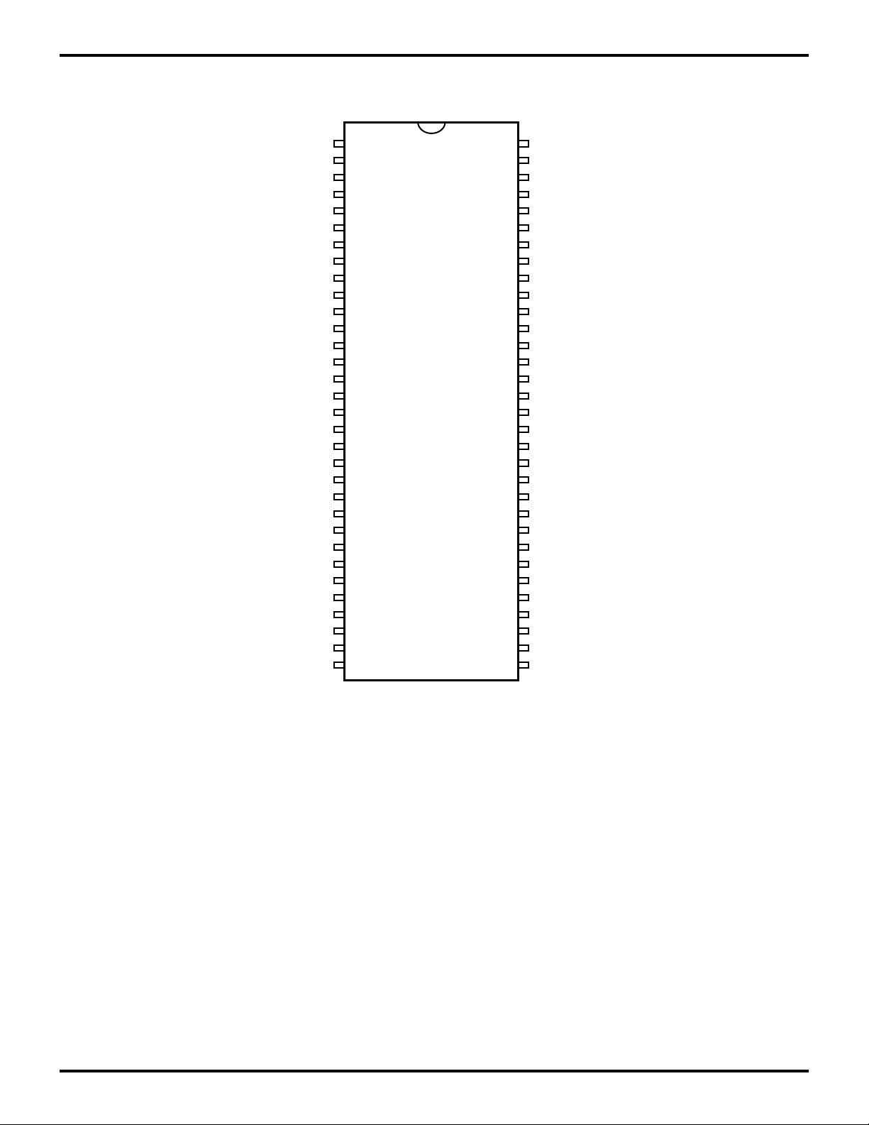
PIN DESCRIPTION
VSS
XTAL
EXTAL
/WAIT
/BUSACK
/BUSREQ
/RESET
/NMI
/INT0
/INT1
/INT2
ST
A0
A1
A2
A3
A4
A5
A6
A7
A8
A9
A10
A11
A12
A13
A14
A15
A16
A17
A18/TOUT
VCC
1
32
Z80180 64-
Pin DIP
64
33
PHI
/RD
/WR
/M1
E
/MREQ
/IORQ
/RFSH
/HALT
/TEND1
/DREQ
CKS
RXS//CTS
TXS
CKA1//TEND0
RXA1
TXA1
CKA//DREQ0
RXA0
TXA0
/DCD0
/CTS0
/RTS0
D7
D6
D5
D4
D3
D2
D1
D0
VSS
DS971800401
Figure 2. Z80180 64-Pin DIP Pin Configuration
P R E L I M I N A R Y
1-3
Z80180/Z8S180/Z8L180
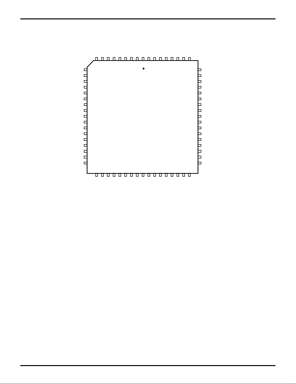
Enhanced Z180 Microprocessor Zilog
/NMI
/RESET
/BUSREQ
/BUSACK
/WAIT
EXTAL
XTAL
VSS
VSS
PHI
/RD
/WR
/M1E/MREQ
/IORQ
/RFSH
/INT0
/INT1
/INT2
ST
A0
A1
A2
A3
VSS
A4
A5
A6
A7
A8
A9
A10
A11
A12
A13
A14
Z80180/Z8S180/
Z8L180
68-Pin PLCC
A15
A16
A17
A18/TOUT
1
VCC
D0D1D2D3D4D5D6
A19
VSS
619
6010
4327
/HALT
/TEND1
/DREQ1
CKS
RXS//CTS1
TXS
CKA1//TEND0
RXA1
TEST
TXA1
CKA0//DREQ0
RXA0
TXA0
/DCD0
/CTS0
/RTS0
D7
Figure 3. Z80180/Z8S180/Z8L180 68-Pin PLCC Pin Configuration
1-4
P R E L I M I N A R Y
DS971800401

1
Z80180/Z8S180/Z8L180
Zilog Enhanced Z180 Microprocessor
/RFSH
N/C
N/C
/HALT
/TEND1
/DREQ1
CKS
RXS/CTS1
TXS
CKA1//TEND0
RXA1
TEST
TXA1
N/C
CKA0//DREQ0
RXA0
TXA0
/DCD0
/CTS0
/RTS0D7N/C
N/C
D6
/IORQ
/MREQ
/M1
/WR
/RD
PHI
VSS
VSS
XTAL
N/C
EXTAL
/WAIT
/BUSACK
/BUSREQ
/RESET
60
65
E
1
/NMI
N/C
5101520
N/C
/INT0
/INT1
/INT2
55 50 45 4164
Z80180/Z8S180/Z8L180
80-Pin QFP
A0A1A2
ST
A3
VSS
A4
A5A6A7A8A9
N/C
A10
A11
N/C
40
N/C
D5
D4
D3
D2
D1
D0
VSS
A19
VCC
A18/TOUT
NC
A17
A16
A15
A14
A13
24
A12
DS971800401
Figure 4. Z80180/Z8S180/Z8L180 80-Pin QFP Pin Configuration
P R E L I M I N A R Y
1-5

Z80180/Z8S180/Z8L180
Enhanced Z180 Microprocessor Zilog
Table 1. Z80180/Z8S180/Z8L180 Pin Identification
Pin Number and Package Type
Default Function
Secondary
Function ControlQFP PLCC DIP
1 9 8 /NMI
2NC
3NC
4 10 9 /INT0
5 11 10 /INT1
6 12 11 /INT2
71312 ST
81413 A0
91514 A1
10 16 15 A2
11 17 16 A3
12 18 V
SS
13 19 17 A4
14 NC
15 20 18 A5
16 21 19 A6
17 22 20 A7
18 23 21 A8
19 24 22 A9
20 25 23 A10
21 26 24 A11
22 NC
23 NC
24 27 25 A12
25 28 26 A13
26 29 27 A14
27 30 28 A15
28 31 29 A16
29 32 30 A17
30 NC
31 33 31 A18 /T
32 34 32 V
CC
OUT
Bit 2 or Bit 3 of TCR
33 35 A19
34 36 33 V
SS
35 37 34 D0
36 38 35 D1
37 39 36 D2
38 40 37 D3
39 41 38 D4
40 42 39 D5
41 43 40 D6
42 NC
43 NC
44 44 41 D7
45 45 42 /RTS0
1-6
P R E L I M I N A R Y
DS971800401

1
Zilog Enhanced Z180 Microprocessor
Table 1. Z80180/Z8S180/Z8L180 Pin Identification
Z80180/Z8S180/Z8L180
Pin Number and Package Type
Default Function
46 46 43 /CTS0
47 47 44 /DCD0
48 48 45 TXA0
49 49 46 RXA0
50 50 47 CKA0 /DREQ0 Bit 3 or Bit 5 of DMODE
51 NC
52 51 48 TXA1
53 52 TEST
54 53 49 RXA1
55 54 50 CKA1 /TEND0 Bit 4 of CNTLA1
56 55 51 TXS
57 56 52 RXS /CTS1 Bit 2 of STAT1
58 57 53 CKS
59 58 54 /DREQ1
60 59 55 /TEND1
61 60 56 /HALT
62 NC
63 NC
64 61 57 /RFSH
65 62 58 /IORQ
66 63 59 /MREQ
67 64 60 E
68 65 61 M1
69 66 62 /WR
70 67 63 /RD
71 68 64 PHI
72 1 1 V
73 2 V
74 3 2 XTAL
75 NC
76 4 3 EXTAL
77 5 4 /WAIT
78 6 5 /BUSACK
79 7 6 /BUSREQ
80 8 7 /RESET
SS
SS
Secondary
Function ControlQFP PLCC DIP
DS971800401
P R E L I M I N A R Y
1-7

Z80180/Z8S180/Z8L180
Enhanced Z180 Microprocessor Zilog
Table 2. Pin Status During RESET BUSACK and SLEEP
Pin Number and Package Type Pin Status
QFP PLCC DIP
Default
Function
Secondary
Function RESET BUSACK
SLEEP
1 9 8 /NMI IN IN IN
2NC
3NC
4 10 9 /INT0 IN IN IN
5 11 10 /INT1 IN IN IN
6 12 11 /INT2 IN IN IN
71312ST 1?1
81413A0 3T 3T 1
91514A1 3T 3T 1
10 16 15 A2 3T 3T 1
11 17 16 A3 3T 3T 1
12 18 V
SS
GND GND GND
13 19 17 A4 3T 3T 1
14 NC
15 20 18 A5 3T 3T 1
16 21 19 A6 3T 3T 1
17 22 20 A7 3T 3T 1
18 23 21 A8 3T 3T 1
19 24 22 A9 3T 3T 1
20 25 23 A10 3T 3T 1
21 26 24 A11 3T 3T 1
22 NC
23 NC
24 27 25 A12 3T 3T 1
25 28 26 A13 3T 3T 1
26 29 27 A14 3T 3T 1
27 30 28 A15 3T 3T 1
28 31 29 A16 3T 3T 1
29 32 30 A17 3T 3T 1
30 NC
31 33 31 A18 /T
32 34 32 V
CC
OUT
3T 3T 1
V
CC
V
CC
V
CC
33 35 A19 3T 3T 1
34 36 33 V
SS
GND GND GND
35 37 34 D0 3T 3T 3T
36 38 35 D1 3T 3T 3T
37 39 36 D2 3T 3T 3T
38 40 37 D3 3T 3T 3T
39 41 38 D4 3T 3T 3T
40 42 39 D5 3T 3T 3T
41 43 40 D6 3T 3T 3T
42 NC
43 NC
44 44 41 D7 3T 3T 3T
1-8
P R E L I M I N A R Y
DS971800401
1
Z80180/Z8S180/Z8L180
Zilog Enhanced Z180 Microprocessor
Table 2. Pin Status During RESET BUSACK and SLEEP
Pin Number and Package Type Pin Status
Default
QFP PLCC DIP
45 45 42 /RTS0 1 OUT 1
46 46 43 /CTS0 IN OUT IN
47 47 44 /DCD0 IN IN IN
48 48 45 TXA0 1 OUT OUT
49 49 46 RXA0 IN IN IN
50 50 47 CKA0 /DREQ0
51 NC
52 51 48 TXA1 1 OUT OUT
53 52 TEST
54 53 49 RXA1 IN IN IN
55 54 50 CKA1 /TEND0
56 55 51 TXS 1 OUT OUT
57 56 52 RXS /CTS1 IN IN IN
58 57 53 CKS 3T I/O I/O
59 58 54 /DREQ1 IN 3T IN
60 59 55 /TEND1 1 OUT 1
61 60 56 /HALT 1 1 0
62 NC
63 NC
64 61 57 /RFSH 1 OUT OUT
65 62 58 /IORQ 1 3T 1
66 63 59 /MREQ 1 3T 1
67 64 60 E 0 OUT OUT
68 65 61 /M1 1 1 1
69 66 62 /WR 1 3T 1
70 67 63 /RD 1 3T 1
71 68 64 PHI OUT OUT OUT
72 1 1 V
73 2 V
74 3 2 XTAL OUT OUT OUT
75 NC
76 4 3 EXTAL IN IN IN
77 5 4 /WAIT IN IN IN
78 6 5 /BUSACK 1 OUT OUT
79 7 6 /BUSREQ IN IN IN
80 8 7 /RESET IN IN IN
Function
SS
SS
Secondary
Function RESET BUSACK
3T OUT OUT
3T IN IN
GND GND GND
GND GND GND
SLEEP
DS971800401
P R E L I M I N A R Y
1-9

Z80180/Z8S180/Z8L180
Enhanced Z180 Microprocessor Zilog
PIN DESCRIPTIONS
A0-A19. Address Bus (Output, active High, tri-state). A0-
A19 form a 20-bit address bus. The Address Bus provides
the address for memory data bus exchanges, up to 1 MB,
and I/O data bus exchanges, up to 64K. The address bus
enters a high-impedance state during reset and external
bus acknowledge cycles. Address line A18 is multiplexed
with the output of PRT channel 1 (T
dress output on reset) and address line A19 is not available in DIP versions of the Z80180.
BUSACK. Bus Acknowledge (Output, active Low).
/BUSACK indicated the requesting device, the MPU address and data bus, and some control signals, have entered their high-impedance state.
/BUSREQ. Bus Request (Input, active Low). This input is
used by external devices (such as DMA controllers) to request access to the system bus. This request has a higher
priority than /NMI and is always recognized at the end of
the current machine cycle. This signal will stop the CPU
from executing further instructions and places address and
data buses, and other control signals, into the high-impedance state.
CKA0, CKA1. Asynchronous Clock 0 and 1 (Bidirectional,
active High). When in output mode, these pins are the
transmit and receive clock outputs from the ASCI baud
rate generators. When in input mode, these pins serve as
the external clock inputs for the ASCI baud rate generators. CKA0 is multiplexed with /DREQ0, and CKA1 is multiplexed with /TEND0.
CKS. Serial Clock (Bidirectional, active High). This line is
clock for the CSIO channel.
PHI CLOCK. System Clock (Output, active High). The out-
put is used as a reference clock for the MPU and the external system. The frequency of this output is equal to onehalf that of the crystal or input clock frequency.
/CTS0 - /CTS1. Clear to send 0 and 1 (Inputs, active Low).
These lines are modem control signals for the ASCI channels. /CTS1 is multiplexed with RXS.
, selected as ad-
OUT
for a read or write operation. These inputs can be programmed to be either level or edge sensed. /DREQ0 is
multiplexed with CKA0.
E. Enable Clock (Output, active High). Synchronous machine cycle clock output during bus transactions.
EXTAL. External Clock Crystal (Input, active High). Crystal oscillator connections. An external clock can be input to
the Z80180/Z8S180/Z8L180 on this pin when a crystal is
not used. This input is Schmitt triggered.
/HALT. Halt/SLEEP (Output, active Low). This output is
asserted after the CPU has executed either the HALT or
SLP instruction, and is waiting for either non-maskable or
maskable interrupt before operation can resume. It is also
used with the /M1 and ST signals to decode status of the
CPU machine cycle.
/INT0. Maskable Interrupt Request 0 (Input, active Low).
This signal is generated by external I/O devices. The CPU
will honor these requests at the end of the current instruction cycle as long as the /NMI and /BUSREQ signals are
inactive. The CPU acknowledges this interrupt request
with an interrupt acknowledge cycle. During this cycle,
both the /M1 and /IORQ signals will become active.
/INT1, /INT2. Maskable Interrupt Request 1 and 2 (Inputs,
active Low). This signal is generated by external I/O devices. The CPU will honor these requests at the end of the
current instruction cycle as long as the /NMI, /BUSREQ,
and /INT0 signals are inactive. The CPU will acknowledge
these requests with an interrupt acknowledge cycle. Unlike
the acknowledgment for /INT0, during this cycle neither
the /M1 or /IORQ signals will become active.
I/O
/IORQ.
indicates that the address bus contains a valid I/O address
for an I/O read or I/O write operation. /IORQ is also generated, along with /M1, during the acknowledgment of the
/INT0 input signal to indicate that an interrupt response
vector can be place onto the data bus. This signal is analogous to the /IOE signal of the Z64180.
Request (Output, active Low, tri-state). /IORQ
D0 - D7. Data Bus = (Bidirectional, active High, tri-state).
D0 - D7 constitute an 8-bit bi-directional data bus, used for
the transfer of information to and from I/O and memory devices. The data bus enters the high-impedance state during reset and external bus acknowledge cycles.
DCD0. Data Carrier Detect 0 (Input, active Low). This is a
programmable modem control signal for ASCI channel 0.
/DREQ0, /DREQ1. DMA Request 0 and 1 (Input, active
Low). /DREQ is used to request a DMA transfer from one
of the on-chip DMA channels. The DMA channels monitor
these inputs to determine when an external device is ready
1-10
P R E L I M I N A R Y
/M1. Machine Cycle 1 (Output, active Low). Together with
/MREQ, /M1 indicates that the current cycle is the Opcode
fetch cycle of and instruction execution. Together with
/IORQ, /M1 indicates that the current cycle is for an interrupt acknowledge. It is also used with the /HALT and ST
signal to decode status of the CPU machine cycle. This
signal is analogous to the /LIR signal of the Z64180.
/MREQ. Memory Request (Output, active Low, tri-state).
/MREQ indicates that the address bus holds a valid address for a memory read or memory write operation. This
signal is analogous to the /ME signal of Z64180.
DS971800401

Z80180/Z8S180/Z8L180
1
Zilog Enhanced Z180 Microprocessor
/NMI. Non-maskable Interrupt (Input, negative edge trig-
gered). /NMI has a higher priority than /INT and is always
recognized at the end of an instruction, regardless of the
state of the interrupt enable flip-flops. This signal forces
CPU execution to continue at location 0066H.
/RD. ReOpcoded (Output, active Low, tri-state). /RD indicated that the CPU wants to read data from memory or an
I/O device. The addressed I/O or memory device should
use this signal to gate data onto the CPU data bus.
/RFSH. Refresh (Output, active Low). Together with
/MREQ, /RFSH indicates that the current CPU machine
cycle and the contents of the address bus should be used
for refresh of dynamic memories. The low order 8 bits of
the address bus (A7 - A10) contain the refresh address.
This signal is analogous to the /REF signal of the
Z64180.
/RTS0. Request to Send 0 (Output, active Low). This is a
programmable modem control signal for ASCI channel 0.
RXA0, RXA1. Receive Data 0 and 1 (Input, active High).
These signals are the receive data to the ASCI channels.
RXS. Clocked Serial Receive Data (Input, active High).
This line is the receiver data for the CSIO channel. RXS is
multiplexed with the /CTS1 signal for ASCI channel 1.
TOUT. Timer Out (Output, active High). T
output from PRT channel 1. This line is multiplexed with
A18 of the address bus.
TXA0, TXA1. Transmit Data 0 and 1 (Outputs, active
High). These signals are the transmitted data from the
ASCI channels. Transmitted data changes are with respect to the falling edge of the transmit clock.
TXS. Clocked Serial Transmit Data (Output, active High).
This line is the transmitted data from the CSIO channel.
/WAIT. Wait (Input, active Low). /WAIT indicated to the
MPU that the addressed memory or I/O devices are not
ready for a data transfer. This input is sampled on the falling edge of T2 (and subsequent wait states). If the input is
sampled Low, then the additional wait states are inserted
until the /WAIT input is sampled high, at which time execution will continue.
/WR. Write (Output, active Low, tri-state).
that the CPU data bus holds valid data to be stored at the
addressed I/O or memory location.
XTAL. Crystal (Input, active High). Crystal oscillator con-
nection. This pin should be left open if an external clock is
used instead of a crystal. The oscillator input is not a TTL
level (reference DC characteristics).
is the pulse
OUT
/WR indicated
ST. Status (Output, active High). This signal is used with
the /M1 and /HALT output to decode the status of the CPU
machine cycle.
Table 3. Status Summary
ST
/HALT /M1
0 1 0 CPU Operation
1 1 0 CPU Operation (2nd opcode and
1 1 1 CPU Operation
0 X 1 DMA Operation
0 0 0 HALT Mode
1 0 1 SLEEP Mode
Notes:
X = Reserved
MC = Machine Cycle
/TEND0, /TEND1. Transfer End 0 and 1 (Outputs, active
Low). This output is asserted active during the last write
cycle of a DMA operation. It is used to indicate the end of
the block transfer. /TEND0 is multiplexed with CKA1.
TEST. Test (Output, not in DIP version). This pin is for test
and should be left open.
Operation
(1st opcode fetch)
3rd Opcode fetch)
(MC except for Opcode fetch)
(including SYSTEM STOP Mode)
Several pins are used for different conditions, depending
on the circumstance.
Multiplexed Pin Descriptions
A18 / /T
CKA0 / /DREQ0 During RESET, this pin is initialized as
CKA1 / /TEND0 During RESET, this pin is initialized as
RXS / /CTS1 During RESET, this pin is initialized as
OUT
During RESET, this pin is initialized as
A18 pin. If either TOC1 or TOC0 bit of
the Timer Control Register (TCR) is set
to 1, TOUT function is selected. If
TOC1 and TOC0 are cleared to 0, A18
function is selected.
CKA0 pin. If either DM1 or SM1 in
DMA Mode Register (DMODE) is set to
1, /DREQ0 function is always selected.
CKA1 pin. If CKA1D bit in ASCI control
register ch1 (CNTLA1) is set to 1,
/TEND0 function is selected. If CKA1D
bit is set to 0, CKA1 function is
selected.
RXS pin. If CTS1E bit in ASCI status
register ch1 (STAT1) is set to 1, /CTS1
function is selected. If CTS1E bit is set
to 0, RXS function is selected.
DS971800401 P R E L I M I N A R Y 1-11

Z80180/Z8S180/Z8L180
Enhanced Z180 Microprocessor Zilog
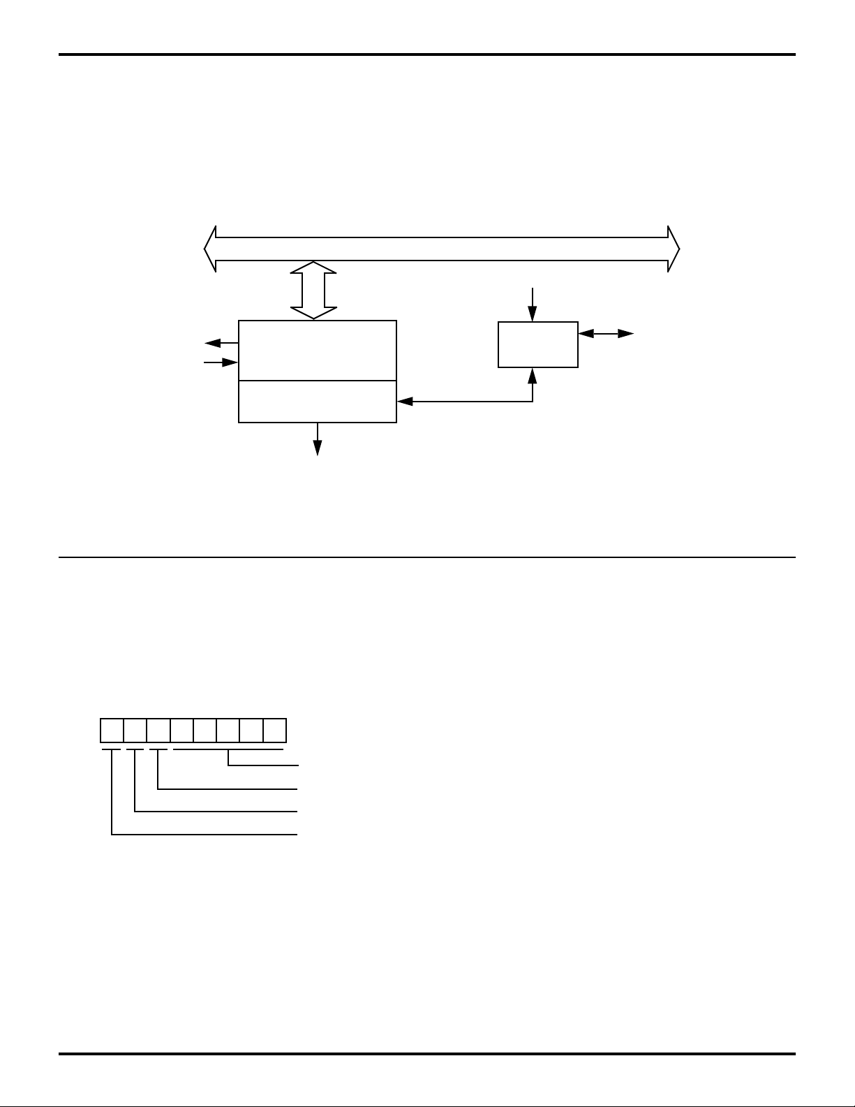
ARCHITECTURE
The Z180® combines a high-performance CPU core with a
variety of system and I/O resources useful in a broad
range of applications. The CPU core consists of five functional blocks: clock generator, bus state controller, Interrupt controller, memory management unit (MMU), and the
central processing unit (CPU). The integrated I/O resources make up the remaining four function blocks: direct
memory access (DMA) control (2 channels), asynchronous serial communication interface (ASCI, 2 channels)
programmable reload timers (PRT, 2 channels), and a
clock serial I/O (CSIO) channel.
Clock Generator. Generates system clock from an external crystal or clock input. The external clock is divided by
two or one and provided to both internal and external devices.
Bus State Controller. This logic performs all of the status
and bus control activity associated with both the CPU and
some on-chip peripherals. This includes wait-state timing,
reset cycles, DRAM refresh, and DMA bus exchanges.
Interrupt Controller. This logic monitors and prioritizes
the variety of internal and external interrupts and traps to
provide the correct responses from the CPU. To maintain
compatibility with the Z80
modes are supported.
Memory Management Unit. The MMU allows the user to
“map” the memory used by the CPU (logically only 64KB)
into the 1 MB addressing range supported by the
Z80180/Z8S180/Z8L180. The organization of the MMU
object code maintains compatibility with the Z80 CPU,
while offering access to an extended memory space. This
is accomplished by using an effective “common areabanked area” scheme.
®
CPU, three different interrupts
Central Processing Unit. The CPU is microcoded to provide a core that is object-code compatible with the Z80
CPU. It also provides a superset of the Z80 instruction set,
including 8-bit multiply. The core has been modified to allow many of the instructions to execute in fewer clock cycles.
DMA Controller. The DMA controller provides high speed
transfers between memory and I/O devices. Transfer operations supported are memory-to-memory, memory
to/from I/O, and I/O-to-I/O. Transfer modes supported are
request, burst, and cycle steal. DMA transfers can access
the full 1 MB address range with a block length up to 64
KB, and can cross over 64K boundaries.
Asynchronous Serial Communication Interface (ASCI). The ASCI logic provides two individual full-duplex
UARTs. Each channel includes a programmable baud rate
generator and modem control signals. The ASCI channels
can also support a multiprocessor communication format
as well as break detection and generation.
Programmable Reload Timers (PRT). This logic consists
of two separate channels, each containing a 16-bit counter
(timer) and count reload register. The time base for the
counters is derived from the system clock (divided by 20)
before reaching the counter. PRT channel 1 provides an
optional output to allow for waveform generation.
1-12 P R E L I M I N A R Y DS971800401
Z80180/Z8S180/Z8L180
1
Zilog Enhanced Z180 Microprocessor
Reset
Timer Data
Register
Timer Reload
Register
TDE Flag
TIF Flag
Timer Data Register
Write (0004H)
FFFFH 0004H 0003H
Timer Reload Register Write (0003H)
FFFFH
0003H
0 < t < 20 φ
20 φ 20 φ 20 φ 20 φ 20 φ 20 φ 20 φ 20 φ 20 φ
0002H 0001H 0000H 0003H 0002H
Reload
Write “1” to TDE
Figure 5. Timer Initialization, Count Down, and Reload Timing
0001H
0000H 0003H
Reload
Timer Data Register Read
Timer Control Requestor Read
φ
TOUT
Timer Data
Reg. = 0001H
Timer Data
Reg. = 0000H
Figure 6. Timer Output Timing
DS971800401 P R E L I M I N A R Y 1-13
Z80180/Z8S180/Z8L180
Enhanced Z180 Microprocessor Zilog
Clocked Serial I/O (CSI/O). The CSIO channel provides a
half-duplex serial transmitter and receiver. This channel
can be used for simple high-speed data connection to another microprocessor or microcomputer. TRDR is used for
both CSI/O transmission and reception. Thus, the system
design must ensure that the constraints of half-duplex operation are met (Transmit and Receive operation cannot
occur simultaneously). For example, if a CSI/O transmis-
Internal Address/Data Bus
TXS
RXS
CSI/O T r ansmit/Receive
Data Register:
TRDR (8)
CSI/O Control Register:
CNTR (8)
Interrupt Request
sion is attempted while the CSI/O is receiving data, a
CSI/O will not work. Also note that TRDR is not buffered.
Therefore, attempting to perform a CSI/O transmit while
the previous transmit data is still being shifted out causes
the shift data to be immediately updated, thereby corrupting the transmit operation in progress. Similarly, reading
TRDR while a transmit or receive is in progress should be
avoided.
φ
Baud Rate
Generator
CKS
Figure 7. CSIO Block Diagram
OPERATION MODES
Z80® versus 64180 Compatibility. The
Z80180/Z8S180/Z8L180 is descended from two different
“ancestor” processors, Zilog's original Z80 and the Hitachi
64180. The Operating Mode Control Register (OMCR),
shown in Figure 8, can be programmed to select between
certain Z80 and 64180differences.
--
D7
D6 D5
--
-- --
Figure 8. Operating Control Register
(OMCR: I/O Address = 3EH)
-Reserved
/IOC (R/W)
/M1TE (W)
M1E (R/W)
M1E (M1 Enable). This bit controls the M1 output and is
set to a 1 during reset.
When M1E=1, the M1 output is asserted Low during the
opcode fetch cycle, the INT0 acknowledge cycle, and the
first machine cycle of the NMI acknowledge.
On the Z80180/Z8S180/Z8L180, this choice makes the
processor fetch an RETI instruction once, and when fetching an RETI from zero-wait-state memory will use three
clock machine cycles, which are not fully Z80-timing compatible but are compatible with the on-chip CTCs.
When M1E=0, the processor does not drive M1 Low during
instruction fetch cycles, and after fetching an RETI instruction once with normal timing, it goes back and re-fetches
the instruction using fully Z80-compatible cycles that include driving M1 Low. This may be needed by some external Z80 peripherals to properly decode the RETI instruction. Figure 9 and Table 4 show the RETI sequence when
M1E=0.
1-14 P R E L I M I N A R Y DS971800401
Z80180/Z8S180/Z8L180
1
Zilog Enhanced Z180 Microprocessor
T1T2T3T1T2T
TITITIT1T2T
3
T1T2T
T
3
I
T
3
I
φ
A0-A18 (A19)
D0-D
7
M1
MREQ
RD
ST
Machine M1
Cycle States Address Data RD WR MREQ IORQ IOC=1 IOC=0 HALT ST
1 T1-T3 1st Opcode EDH 0 1 0 1 0 1 1 0
2 T1-T3 2nd Opcode 4DH 0 1 0 1 0 1 1 0
Ti NA Tri-State 1 1 1 1 1 1 1 1
Ti NA Tri-State 1 1 1 1 1 1 1 1
Ti NA Tri-State 1 1 1 1 1 1 1 1
3 T1-T3 1st Opcode EDH 0 1 0 1 0 0 1 1
Ti NA Tri-State 1 1 1 1 1 1 1 1
4 T1-T3 2nd Opcode 4DH 0 1 0 1 0 1 1 1
5 T1-T3 SP Data 0 1 0 1 1 1 1 1
6 T1-T3 SP+1 Data 0 1 0 1 1 1 1 1
PC
EDH
Figure 9. RETI Instruction Sequence with MIE=0
Table 4. RETI Control Signal States with MIE=0
PC+1
4DH EDH
PC PC+1
4DH
M1TE (M1 Temporary Enable). This bit controls the temporary assertion of the /M1 signal. It is always read back
as a 1 and is set to 1 during reset.
When M1E is set to 0 to accommodate certain external
Z80 peripheral(s), those same device(s) may require a
pulse on M1 after programming certain of their registers to
complete the function being programmed.
DS971800401 P R E L I M I N A R Y 1-15
For example, when a control word is written to the Z80 PIO
to enable interrupts, no enable actually takes place until
the PIO sees an active M1 signal. When M1TE=1, there is
no change in the operation of the /M1 signal and M1E controls its function. When M1TE=0, the M1 output will be asserted during the next opcode fetch cycle regardless of the
state programmed into the M1E bit. This is only momentary (one time) and the user need not preprogram a 1 to
disable the function (see Figure10).
Z80180/Z8S180/Z8L180
Enhanced Z180 Microprocessor Zilog
T
1
T
2
T
φ
/WR
/M1
Write into OMCR
Figure 10. M1 Temporary Enable Timing
IOC. This bit controls the timing of the /IORQ and /RD sig-
nals. It is set to 1 by reset.
T
1
T
φ
/IORQ
/RD
3
T
1
T
2
T
3
Opcode Fetch
When /IOC=1, the /IORQ and /RD signals function the
same as the Z64180 (Figure 11).
2
T
W
T
3
/WR
Figure 11. I/O Read and Write Cycles with IOC = 1
When /IOC = 0, the timing of the /IORQ and RD
signals
match the timing of the Z80. The /IORQ and /RD signals
T
1
T
φ
/IORQ
/RD
/WR
Figure 12. I/O Read and Write Cycles with IOC = 0
go active as a result of the rising edge of T2. (Figure 12.)
2
T
W
T
3
1-16 P R E L I M I N A R Y DS971800401
Z80180/Z8S180/Z8L180
1
Zilog Enhanced Z180 Microprocessor
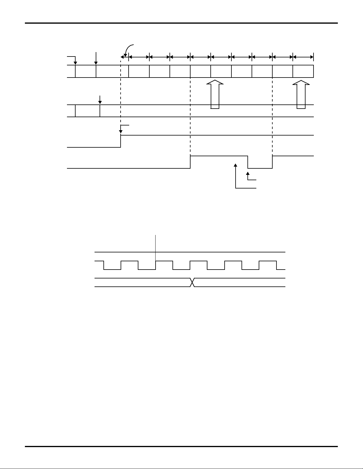
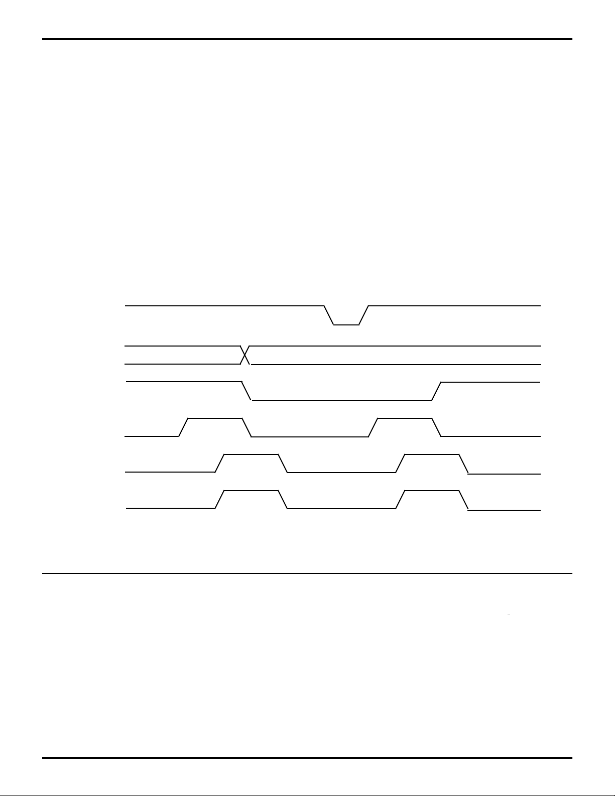
HALT and Low-Power Operating Modes. The
Z80180/Z8S180/Z8L180 can operate in seven modes with
respect to activity and power consumption:
– Normal Operation
– HALT Mode
– IOSTOP Mode
– SLEEP Mode
– SYSTEM STOP Mode
– IDLE Mode
– STANDBY Mode (with or without QUICK
RECOVERY)
Normal Operation. The Z80180/Z8S180/Z8L180 processor is fetching and running a program. All enabled functions and portions of the device are active, and the HALT
pin is High.
, NMI
INT
i
HALT Mode. This mode is entered by the HALT instruction. Thereafter, the Z80180/Z8S180/Z8L180 processor
continually fetches the following opcode but does not execute it, and drives the HALT, ST and M1 pins all Low. The
oscillator and PHI pin remain active, interrupts and bus
granting to external masters, and DRAM refresh can occur
and all on-chip I/O devices continue to operate including
the DMA channels.
The Z80180/Z8S180/Z8L180 leaves HALT mode in response to a Low on RESET, on to an interrupt from an enabled on-chip source, an external request on NMI, or an
enabled external request on INT0, INT1, or INT2. In case
of an interrupt, the return address will be the instruction following the HALT instruction; at that point the program can
either branch back to the HALT instruction to wait for another interrupt, or can examine the new state of the system/application and respond appropriately.
A
0-A19
/HALT
/M1
/MREQ
/RD
SLEEP Mode. This mode is entered by keeping the
IOSTOP bit (ICR5) bits 3 and 6 of the CPU Control Register (CCR3, CCR6) all zero and executing the SLP instruction. The oscillator and PHI output continue operating, but
are blocked from the CPU core and DMA channels to reduce power consumption. DRAM refresh stops but interrupts and granting to external master can occur. Except
when the bus is granted to an external master, A19-0 and
all control signals except /HALT are maintained High.
/HALT is Low. I/O operations continue as before the SLP
instruction, except for the DMA channels.
HALT Opcode Address
Figure 13. HALT Timing
HALT Opcode Address + 1
The Z80180/Z8S180/Z8L180 leaves SLEEP mode in response to a low on /RESET, an interrupt request from an
on-chip source, an external request on /NMI, or an external
request on /INT0, 1, or 2.
DS971800401 P R E L I M I N A R Y 1-17
Z80180/Z8S180/Z8L180
Enhanced Z180 Microprocessor Zilog
If an interrupt source is individually disabled, it cannot
bring the Z80180/Z8S180/Z8L180 out of SLEEP mode. If
an interrupt source is individually enabled, and the IEF bit
is 1 so that interrupts are globally enabled (by an EI instruction), the highest priority active interrupt will occur,
with the return address being the instruction after the SLP
instruction. If an interrupt source is individually enabled,
but the IEF bit is 0 so that interrupts are globally disabled
(by a DI instruction), the Z80180/Z8S180/Z8L180 leaves
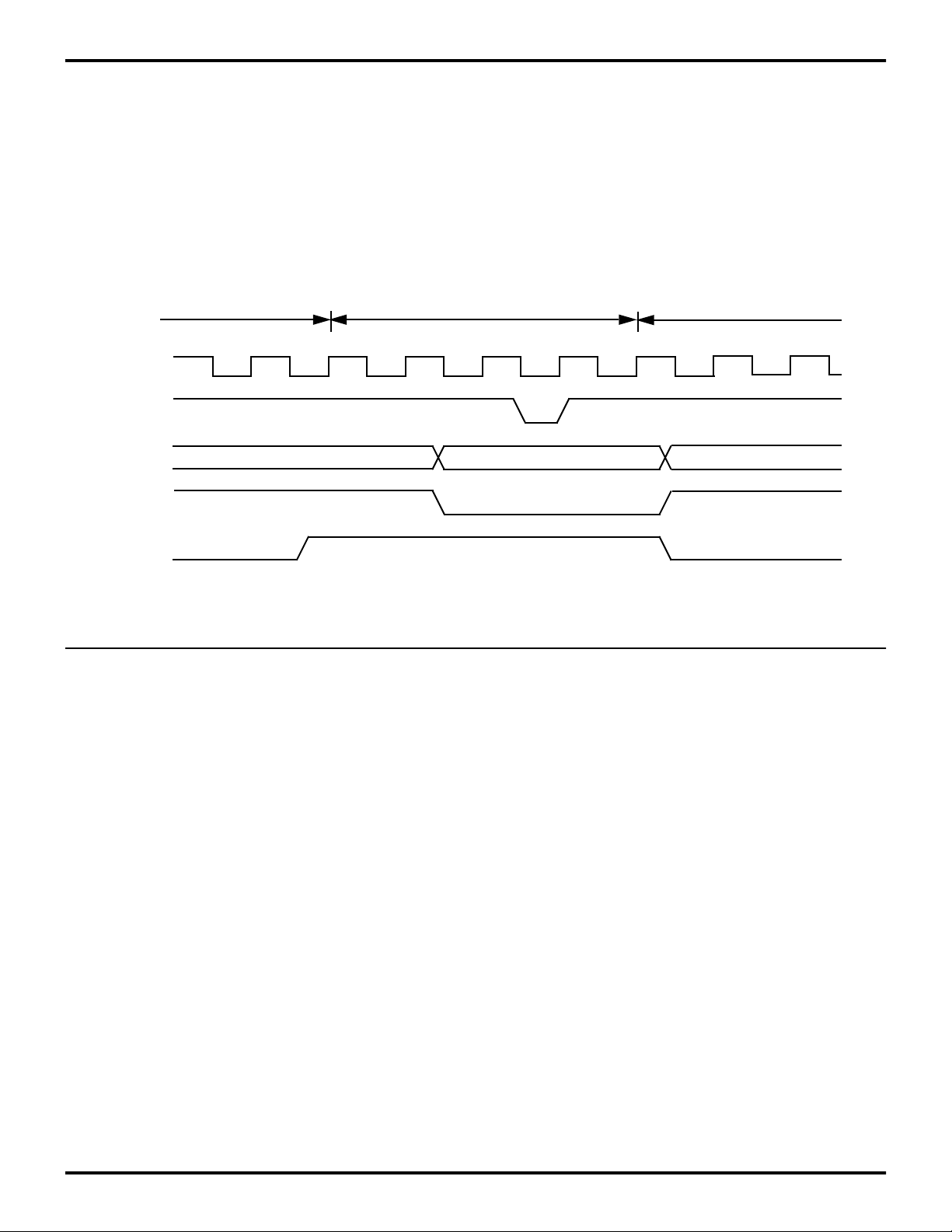
SLP 2nd Opcode
Fetch Cycle
T
2
T
3
T
1
SLEEP Mode
T
2
φ
/INTi, /NMI
A
0-A19
/HALT
SLP 2nd Opcode Address
SLEEP mode by simply executing the following instruction(s).
This provides a technique for synchronization with highspeed external events without incurring the latency imposed by an interrupt response sequence. Figure 14
shows the timing for exiting SLEEP mode due to an interrupt request. Note that the Z80180/Z8S180/Z8L180 takes
about 1.5 clocks to restart.
Opcode Fetch or Interrupt
Acknowledge Cycle
T
S
T
S
T
1
T
2
T
3
FFFFFH
M1
Figure 14. SLEEP Timing
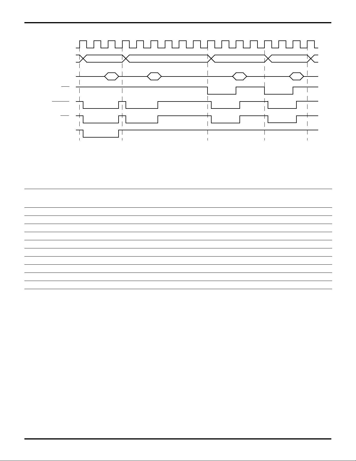
IOSTOP Mode. IOSTOP mode is entered by setting the
IOSTOP bit of the I/O Control Register (ICR) to 1. In this
case, on-chip I/O (ASCI, CSI/O, PRT) stops operating.
However, the CPU continues to operate. Recovery from
IOSTOP mode is by resetting the IOSTOP bit in ICR to 0.
SYSTEM STOP Mode. SYSTEM STOP mode is the combination of SLEEP and IOSTOP modes. SYSTEM STOP
mode is entered by setting the IOSTOP bit in ICR to 1 followed by execution of the SLP instruction. In this mode,
on-chip I/O and CPU stop operating, reducing power consumption, but the PHI output continues to operate. Recovery from SYSTEM STOP mode is the same as recovery
from SLEEP mode except that internal I/O sources (disabled by IOSTOP) cannot generate a recovery interrupt.
IDLE Mode. Software can put the
Z80180/Z8S180/Z8L180 into this mode by setting the
IOSTOP bit (ICR5) to 1, CCR6 to 0, CCR3 to 1 and executing the SLP instruction. The oscillator keeps operating
but its output is blocked to all circuitry including the PHI
pin. DRAM refresh and all internal devices stop, but external interrupts can occur. Bus granting to external masters
can occur if the BREST bit in the CPU control Register
(CCR5) was set to 1 before IDLE mode was entered.
The Z80180/Z8S180/Z8L180 leaves IDLE mode in response to a Low on RESET, an external interrupt request
on NMI, or an external interrupt request on /INT0, /INT1 or
/INT2 that is enabled in the INT/TRAP Control Register. As
previously described for SLEEP mode, when the
Z80180/Z8S180/Z8L180 leaves IDLE mode due to an
NMI, or due to an enabled external interrupt request when
the IEF flag is 1 due to an EI instruction, it starts by performing the interrupt with the return address being that of
the instruction after the SLP instruction.
If an external interrupt enables the INT/TRAP control register while the IEF1 bit is 0, Z80180/Z8S180/Z8L180
leaves IDLE mode; specifically, the processor restarts by
executing the instructions following the SLP instruction.
1-18 P R E L I M I N A R Y DS971800401
Z80180/Z8S180/Z8L180
1
Zilog Enhanced Z180 Microprocessor
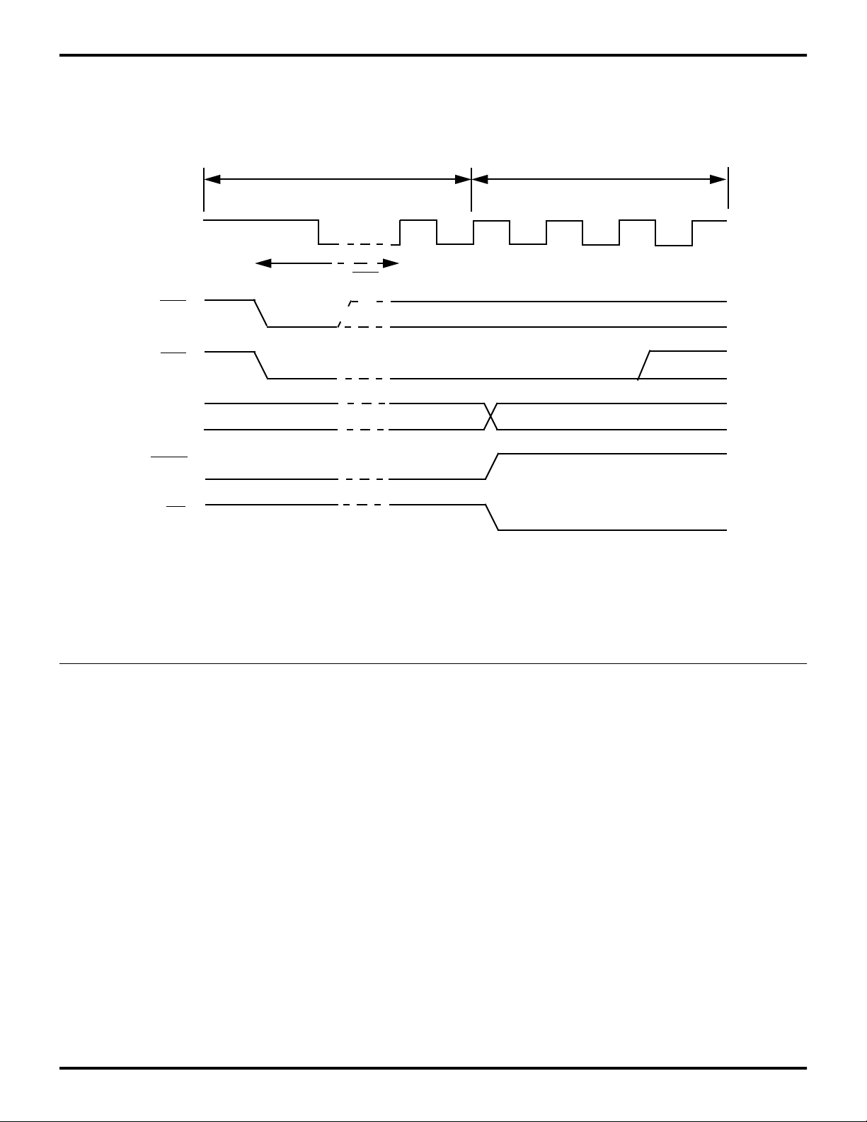
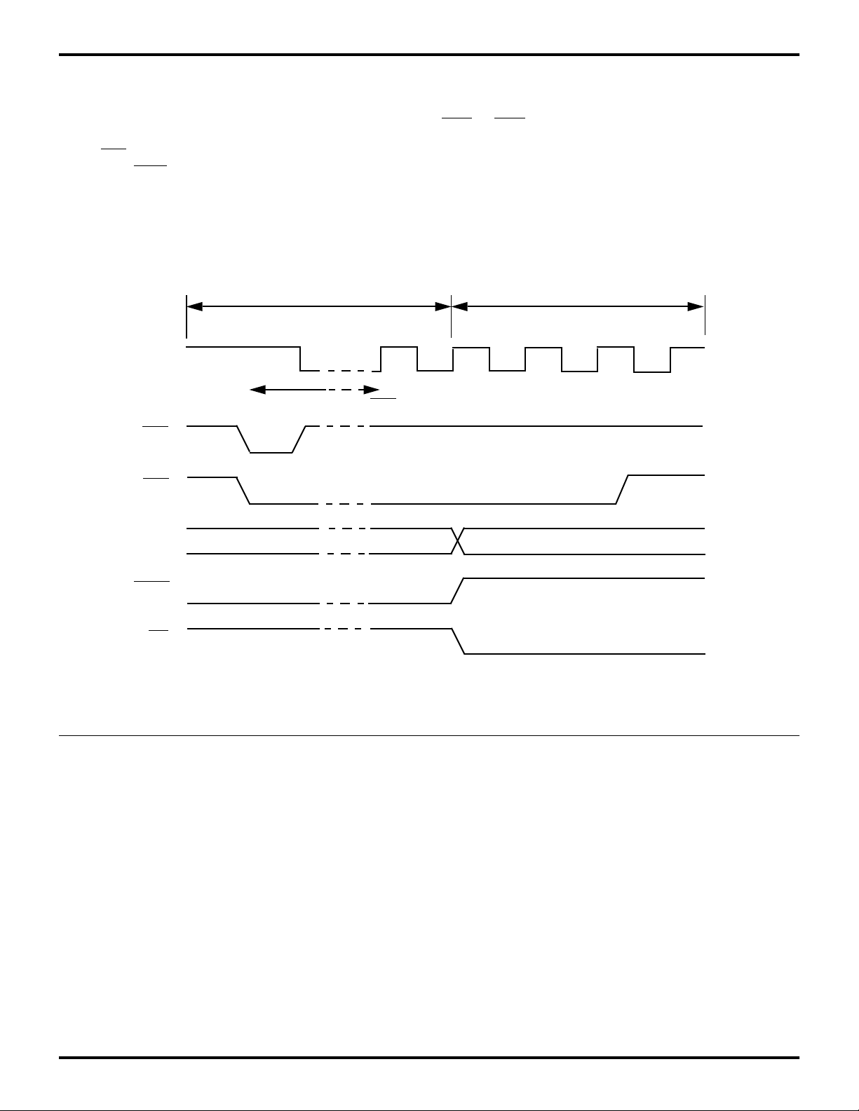
Figure 15 shows the timing for exiting IDLE mode due to
an interrupt request. Note that the
IDLE Mode
φ
9.5 Cycle Delay from INTi Asserted
NMI
or
INTi
A19-A
0
HALT
FFFFFH
Z80180/Z8S180/Z8L180 takes about 9.5 clocks to restart.
Opcode Fetch or Interrupt
Acknowledge Cycle
T
1
T
2
T
3
T
4
M1
Figure 15. Z80180/Z8S180/Z8L180 IDLE Mode Exit due to External Interrupt
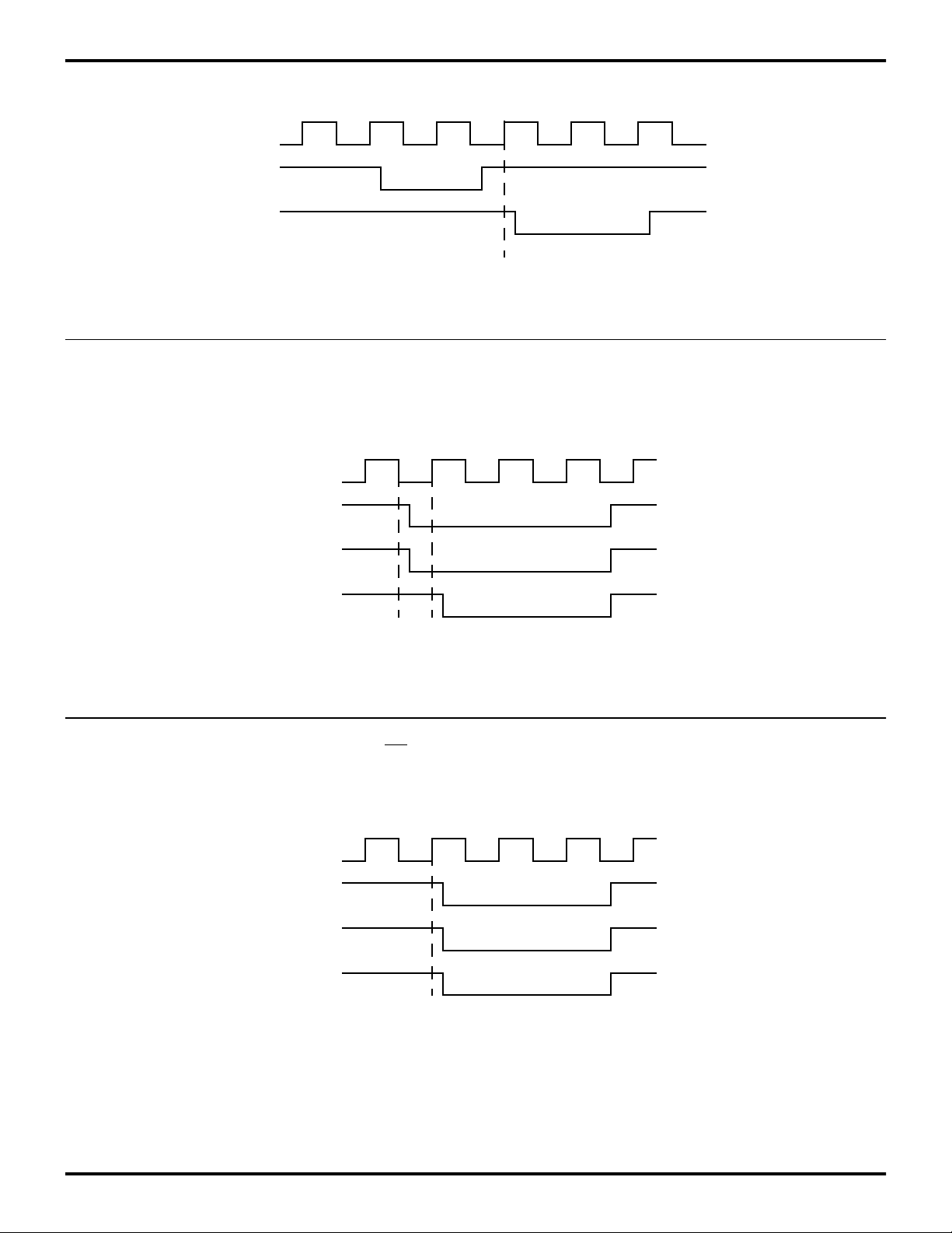
While the Z80180/Z8S180/Z8L180 is in IDLE mode, it will
grant the bus to an external master if the BREXT bit
(CCR5) is 1. Figure 16 shows the timing for this sequence.
Note that the part takes 8 clock cycles longer to respond to
the Bus Request than in normal operation.
After the external master negates the Bus Request, the
Z80180/Z8S180/Z8L180 disables the PHI clock and remains in IDLE mode.
DS971800401 P R E L I M I N A R Y 1-19
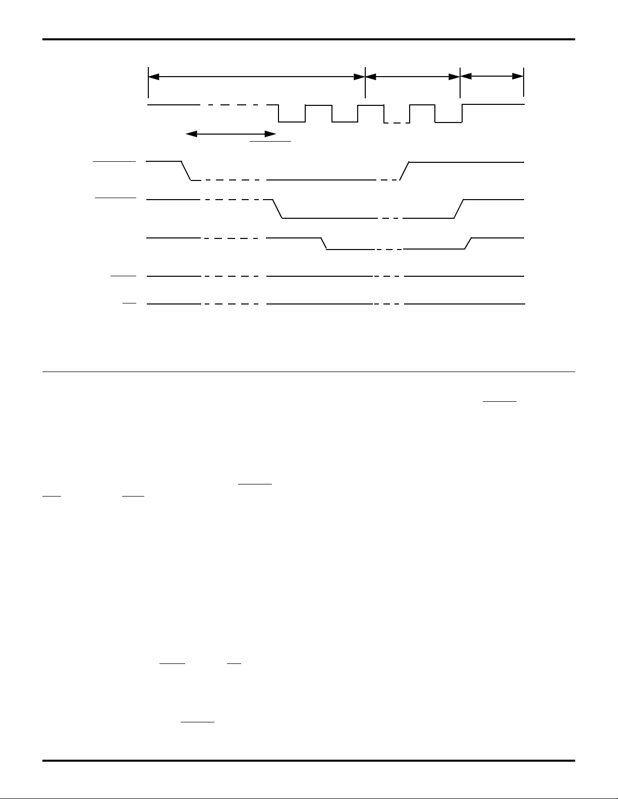
Z80180/Z8S180/Z8L180
Enhanced Z180 Microprocessor Zilog
φ
BUSREQ
BUSACK
A19-A
HALT
M1
IDLE Mode
9.5 Cycle Delay until BUSACK Asserted
0
High
Low
Figure 16. Bus Granting to External Master in IDLE Mode
FFFFFH
Bus RELEASE Mode
TX
High Impedance
TX
IDLE Mode
FFFFFH
STANDBY Mode (With or Without QUICK RECOVERY).
Software can put the Z80180/Z8S180/Z8L180 into this
mode by setting the IOSTOP bit (ICR5) to 1 and CCR6 to
1, and executing the SLP instruction. This mode stops the
on-chip oscillator and thus draws the least power of any
mode, less than 10µµA.
As with IDLE mode, the Z80180/Z8S180/Z8L180 will leave
STANDBY mode in response to a Low on RESET
, or a Low on INT0-2 that is enabled by a 1 in the cor-
NMI
responding bit in the INT/TRAP Control Register, and will
grant the bus to an external master if the BREXT bit in the
CPU Control Register (CCR5) is 1. But the time required
for all of these operations is greatly increased by the need
to restart the on-chip oscillator and ensure that it has stabilized to square-wave operation.
When an external clock is connected to the EXTAL pin
rather than a crystal to the XTAL and EXTAL pins, and the
external clock runs continuously, there is little need to use
STANDBY mode because there is no time required to restart the oscillator, and other modes restart faster. However, if external logic stops the clock during STANDBY mode
(for example, by decoding HALT Low and M1 High for several clock cycles), then STANDBY mode can be useful to
allow the external clock source to stabilize after it is re-enabled.
When external logic drives RESET Low to being a
Z80180/Z8S180/Z8L180 out of STANDBY mode, and a
or on
crystal is used or an external clock source has been
stopped, the external logic must hold RESET
on-chip oscillator or external clock source has restarted
and stabilized.
The clock stability requirements of the
Z80180/Z8S180/Z8L180 are much less in the divide-bytwo mode that's selected by a Reset sequence and thereafter controlled by the Clock Divide bit in the CPU Control
Register (CCR7). Because of this, software should:
a. Program CCR7 to 0 to select divide-by-two mode,
before the SLP instruction that enters STANDBY
mode, and.
b. After a Reset, interrupt or in-line restart after the
SLP 01 instruction, delay programming CCR7
back to 1 to set divide-by-one mode, as long as
possible to allow additional clock stabilization
time.
If software sets CCR6 to 1 before the SLP instruction places the MPU in STANDBY mode, the value in the CCR3 bit
determines how long the Z80180/Z8S180/Z8L180 will wait
for oscillator restart and stabilization when it leaves
STANDBY mode due to an external interrupt request. If
CCR3 is 0, the Z80180/Z8S180/Z8L180 waits 217
(131,072) clock cycles, while if CCR3 is 1, it waits only 64
clock cycles. The latter is called QUICK RECOVERY
mode. The same delay applies to granting the bus to an
Low until the
1-20 P R E L I M I N A R Y DS971800401
Z80180/Z8S180/Z8L180
1
Zilog Enhanced Z180 Microprocessor
external master during STANDBY mode, when the BREXT
bit in the CPU Control Register (CCR5) is 1.
As described previously for SLEEP and IDLE modes,
when a Z80180/Z8S180/Z8L180 leaves STANDBY mode
due to NMI Low, or when it leaves STANDBY mode due to
an enabled INTO-2 low when the IEF, flag is 1 due to an
IE instruction, it starts by performing the interrupt with the
return address being that of the instruction following the
SLP instruction. If the Z80180/Z8S180/Z8L180 leaves
STANDBY mode due to an external interrupt request that's
STANDBY Mode
φ
217 or 64 Cycle Delay from INTi Asserted
NMI
or
enabled in the INT/TRAP Control Register, but the IEF, bit
is 0 due to a DI instruction, the processor restarts by executing the instruction(s) following the SLP instruction. If
INT0, or INT1 or 2 goes inactive before the end of the clock
stabilization delay, the Z80180/Z8S180/Z8L180 stays in
STANDBY mode.
Figure 17 shows the timing for leaving STANDBY mode
due to an interrupt request. Note that the
Z80180/Z8S180/Z8L180 takes either 64 or 217 (131,072)
clocks to restart, depending on the CCR3 bit.
Opcode Fetch or Interrupt
Acknowledge Cycle
T
1
T
2
T
3
T
4
INTi
A19-A
0
HALT
M1
Figure 17. Z80180/Z8S180/Z8L180 STANDBY Mode Exit due to External Interrupt
While the Z80180/Z8S180/Z8L180 is in STANDBY mode,
it will grant the bus to an external master if the BREXT bit
(CCR5) is 1. Figure 18 shows the timing of this sequence.
Note that the part takes 64 or 217 (131,072) clock cycles
to grant the bus depending on the CCR3 bit.
FFFFFH
The latter (non-Quick-Recovery) case may be prohibitive
for many “demand driven” external masters. If so, QUICK
RECOVERY or IDLE mode can be used.
DS971800401 P R E L I M I N A R Y 1-21

Z80180/Z8S180/Z8L180
Enhanced Z180 Microprocessor Zilog
BUSREQ
BUSACK
A19-A
HALT
M1
STANDBY Mode
φ
64 or 217 Cycle Delay after BUSREQ Asserted
0
Low
High
FFFFFH
Bus Release Mode
TX
TX
STANDBY Mode
FFFFFH
Figure 18. Bus Granting to External Master During STANDBY Mode
1-22 P R E L I M I N A R Y DS971800401

Z80180/Z8S180/Z8L180
1
Zilog Enhanced Z180 Microprocessor
STANDARD TEST CONDITIONS
The DC Characteristics and Capacitance sections above
+5 V
apply to the following standard test conditions, unless otherwise noted. All voltages are referenced to GND (0V).
Positive current flows in to the referenced pin.
All AC parameters assume a load capacitance of 100 pF.
From Output
Under Test
Add 10 ns delay for each 50 pF increase in load up to a
maximum of 200 pF for the data bus and 100 pF for the address and control lines. AC timing measurements are referenced to 1.5 volts (except for CLOCK, which is refer-
100 pF
250
µA
enced to the 10% and 90% points). The Ordering
Information section lists temperature ranges and product
numbers. Package drawings are in the Package Information section. Refer to the Literature List for additional documentation.
Figure 19. AC Load Capacitance Parameters
ABSOLUTE MAXIMUM RATINGS
Item Symbol Value Unit
Supply V oltage V
Input V oltage V
Operating Temperature T
Extended Temperature T
Storage Temperature T
cc
in
opr
ext
stg
-0.3 ~ +7.0 V
-0.3 ~ Vcc +0.3 V
0 ~ 70 °C
-40 ~ 85 °C
-55 ~ +150 °C
2.1k
Note: Permanent LSI damage may occur if maximum
ratings are exceeded. Normal operation should be under
recommended operating conditions. If these conditions
are exceeded, it could affect reliability of LSI.
DS971800401 P R E L I M I N A R Y 1-23

Z80180/Z8S180/Z8L180
Enhanced Z180 Microprocessor Zilog
DC CHARACTERISTICS
Note: Vcc = 5V + 10%, Vss = 0V over specified temperature range unless otherwise noted.
Symbol Item Condition Min. Typ. Max. Unit
V
IH1
V
IH2
V
IH3
V
IL1
V
IL2
V
OH
V
OL
I
IL
I
TL
ICC* Power Dissipation*
C
P
Note: **
V
= VCC -1.0V, V
IHmin
Input “H” Voltage
/RESET, EXTAL, /NMI
Input “H” Voltage
Except /RESET, EXTAL, /NMI
Input “H” Voltage
Except CKS, CKA0, CKA1
Input “L” Voltage
/RESET, EXTAL, /NMI
Input “L” Voltage
Except /RESET, EXTAL, /NMI
Outputs “H” Voltage
All outputs
Outputs “L” Voltage
IOH = -200 µA 2.4 – – V
I
= -20 µAV
OH
IOL = -2.2 µA – – 0.45 V
All outputs
Input Leakage
VIN = 0.5 ~ Vcc -0.5 – – 1.0 µA
Current All Inputs
Except XTAL, EXTAL
Three State Leakage
VIN = 0.5 ~ Vcc -0.5 – – 1.0 µA
Current
F = 6 MHz – 15 40 MA
(Normal Operation)
F = 8 MHz – 20 50
F = 10 MHz** – 25 60
Power Dissipation*
(SYSTEM STOP mode)
F = 6 MHz – 3.8 12.5
F = 8 MHz – 5 15
F = 10 MHz** – 6.3 17.5
Pin Capacitance VIN = 0V, f = 1 MHz
Ta = 25° C
= 0.8V (all output terminals are at no load.) VCC = 5.0V
ILmax
Vcc -0.6 – Vcc +0.3 V
2.0 – Vcc +0.3 V
2.4 – Vcc +0.3 V
-0.3 – 0.6 V
-0.3 – 0.8 V
-1.2 – –
cc
– – 12 pF
1-24 P R E L I M I N A R Y DS971800401

Z80180/Z8S180/Z8L180
1
Zilog Enhanced Z180 Microprocessor
AC CHARACTERISTICS
Vcc = 5V + 10%, Vss = 0V, TA - 0 to +70° C, unless otherwise noted.
Z80180-6 Z80180-8 Z80180-10
No. Symbol Item
1. t
2. t
3. t
4. t
5. t
6. t
7. t
8. t
9. t
cyc
CHW
CLW
cf
cr
AD
AS
MED1
RDD1
Clock Cycle Time 162 2000 125 2000 100 2000 ns
Clock “H” Pulse Width 65 – 50 – 40 – ns
Clock “L” Pulse Width 65 – 50 – 40 – ns
Clock Fall Time – 15 – 15 – 10 ns
Clock Rise Time – 15 – 15 – 10 ns
ØRise to Address Valid Delay – 90 – 80 – 70 ns
Address Valid to /MREQ Fall or /IORQ Fall)
Ø Fall to /MREQ Fall Delay
Ø Fall to /RD Fall Delay /IOC = 1
Ø Rise to /RD Rise
10. t
11. t
M1D1
AH
Ø Rise to /M1 Fall Delay
Address Hold Time from
Delay /IOC = 0
30–20–10–ns
–60–50–50ns
–60–50–50ns
–65–60–55
–80–70–60ns
35–20–10–ns
UnitMin. Max. Min. Max. Min. Max.
(/MREQ, /IOREQ, /RD, /WR)
12. t
13. t
14. t
15. t
16. t
17. t
18. t
19. t
20. t
21. t
22. t
23. t
24. t
25. t
26. t
MED2
RDD2
M1D2
DRS
DRH
STD1
STD2
WS
WH
WDZ
WRD1
WDD
WDS
WRD2
WRP
Ø Fall to /MREQ Rise Delay
Ø Fall to /RD Rise Delay
Ø Rise to /M1 Rise Delay
Data Read Set-up Time 40 – 30 – 25 – ns
Data Read Hold Time 0–0–0–ns
Ø Fall to ST Fall Delay
Ø Fall to ST Rise Delay
/WAIT Set-up Time to Ø Fall 40 – 40 – 30 – ns
/WAIT Hold Time from Ø Fall 40 – 40 – 30 – ns
Ø Rise to Data Float Delay – 95 – 70 – 60 ns
Ø Rise to /WR Fall Delay
Ø Fall to Write Data Delay Time – 90 – 80 – 60 ns
Write Data Set-up Time to /WR Fall 40 – 20 – 15 – ns
Ø Fall to /WR Rise Delay
/WR Pulse Width 170 – 130 – 110 – ns
–60–50–50ns
–60–50–50ns
–80–70*–60ns
–90–70–60ns
–90–70–60ns
–65–60–50ns
–80–60–50ns
26a. /WR Pulse Width (I/O Write Cycle) 332 – 255 – 210 – ns
27. t
28. t
29. t
30. t
31. t
32. t
33. t
34. t
35. t
36. t
37. t
38. t
39. t
WDH
IOD1
IOD2
IOD3
INTS
INTS
NMIW
BRS
BRH
BAD1
BAD2
BZD
MEWH
Write Data Hold Time from (/WR Rise)
Ø Fall to /IORQ Fall Delay /IOC = 1
Ø Rise to /IORQ Fall
Delay /IOC = 1
Ø Fall to /IORQ Rise Delay
/M1 Fall to /IORQ Fall Delay
/INT Set-up Time to Ø Fall 40 – 40 – 30 – ns
/INT Hold Time from Ø Fall 40 – 40 – 30 – ns
/NMI Pulse Width 120 – 100 – 80 – ns
/BUSREQ Set-up Time to Ø Fall 40 – 40 – 30 – ns
/BUSREQ Hold Time from Ø Fall 40 – 40 30 ns
Ø Rise to /BUSACK Fall Delay
Ø Fall to /BUSACK Rise Delay
Ø Rise to Bus Floating Delay Time – 125 – 90 – 80 ns
/MREQ Pulse Width (HIGH) 110 – 90 – 70 – ns
40–15–10–
–60–50–50ns
–65–60–55
–60–50–50ns
340 – 250 – 200 – ns
–95–70–60ns
–90–70–60ns
DS971800401 P R E L I M I N A R Y 1-25

Z80180/Z8S180/Z8L180
Enhanced Z180 Microprocessor Zilog
Z80180-6 Z80180-8 Z80180-10
No. Symbol Item
40. t
41. t
42. t
43. t
44. t
45. t
46. t
47. t
48. t
49. t
50. t
51. P
52. P
53. t
54. t
55. t
56. t
MEWL
RFD1
RFD2
HAD1
HAD2
DRQS
DRQH
TED1
TED2
ED1
ED2
Er
Ef
TOD
STDI
/MREQ Pulse Width (LOW) 125 – 100 – 80 – ns
Ø Rise to /RFSH Fall Delay – 90 – 80 – 60 ns
Ø Rise to /RFSH Rise Delay – 90 – 80 – 60 ns
Ø Rise to /HALT Fall Delay – 90 – 80 – 50 ns
Ø Rise to /HALT Rise Delay – 90 – 80 – 50 ns
/DREQi Set-up Time to Ø Rise 40 – 40 – 30 – ns
/DREQi Hold Time from Ø Rise 40 – 40 – 30 – ns
Ø Fall to /TENDi Fall Delay – 70 – 60 – 50 ns
Ø Fall to /TENDI Rise Delay – 70 – 60 – 50 ns
Ø Rise to E Rise Delay – 95 – 70 – 60 ns
Ø Fall or Rise to E Fall Delay – 95 – 70 – 60 ns
E Pulse Width (HIGH) 75 – 65 – 55 – ns
WEH
E Pulse Width (LOW) 180 – 130 – 110 – ns
WEL
Enable Rise Time – 20 – 20 – 20 ns
Enable Fall Time – 20 – 20 – 20 ns
Ø Fall to Timer Output Delay – 300 – 200 – 150 ns
CSI/O Transmit Data Delay Time (Internal
Clock Operation)
57. t
STDE
CSI/O Transmit Data Delay Time (External
Clock Operation)
58. t
SRSI
CSI/O Receive Data Set-up Time (Internal
Clock Operation)
59. t
SRHI
CSI/O Receive Data Hold Time (Internal
Clock Operation)
60. t
SRSE
CSI/O Receive Data Set-up Time (External
Clock Operation)
61. t
SRHE
CSI/O Receive Data Hold Time (External
Clock Operation)
62. t
63. t
64. t
65. t
66. t
67. t
68. t
69. t
70. t
RES
REH
OSC
EXr
EXf
Rr
Rf
Ir
If
/RESET Set-up Time to Ø Fall 120 – 100 – 80 – ns
/RESET Hold Time from Ø Fall 80 – 70 – 50 – ns
Oscillator Stabilization Time – 20 – 20 – TBD ns
External Clock Rise Time (EXTAL) – 25 – 25 – 25 ns
External Clock Fall Time (EXTAL) – 25 – 25 – 25 ns
/RESET Rise Time – 50 – 50 – 50 ns
/RESET Fall Time – 50 – 50 – 50 ns
Input Rise Time (except EXTAL, /RESET) – 100 – 100 – 100 ns
Input Fall Time (except EXTAL, /RESET) – 100 – 100 – 100 ns
UnitMin. Max. Min. Max. Min. Max.
– 200 – 200 – 150 ns
– 7.5tcyc
+300
– 7.5tcyc
+200
– 7.5tcyc
+150
ns
1–1–1–tcyc
1–1–1–tcyc
1–1–1–tcyc
1–1–1–tcyc
1-26 P R E L I M I N A R Y DS971800401

Z80180/Z8S180/Z8L180
1
Zilog Enhanced Z180 Microprocessor
AC CHARACTERISTICS
= 5V ±10% or VCC = 3.3V ±10% over specified temperature range, unless otherwise noted, 33
(V
CC
MHZ characteristics apply only to 5V operation.)
Z80180-20 Z80180-33
No. Symbol Item
1. t
2. t
3. t
4. t
5. t
6. t
7. t
8. t
9. t
10. t
11. t
cyc
CHW
CLW
cf
cr
AD
AS
MED1
RDD1
M1D1
AH
Clock Cycle Time 50 2000 33 2000 ns
Clock “H” Pulse Width 15 – 10 – ns
Clock “L” Pulse Width 15 – 10 – ns
Clock Fall Time – 10 – 5 ns
Clock Rise Time – 10 – 5 ns
ØRise to Address Valid Delay – 15 – 15 ns
Address Valid to /MREQ Fall or /IORQ Fall)
Ø Fall to /MREQ Fall Delay
Ø Fall to /RD Fall Delay /IOC = 1
Ø Rise to /RD Rise
Delay /IOC = 0
Ø Rise to /M1 Fall Delay
Address Hold Time from
20 – 5 – ns
–15–15ns
–15–15ns
–15–15
–15–15ns
–205 –ns
(/MREQ, /IOREQ, /RD, /WR)
12. t
13. t
14. t
15. t
16. t
17. t
18. t
19. t
20. t
21. t
22. t
23. t
24. t
25. t
26. t
MED2
RDD2
M1D2
DRS
DRH
STD1
STD2
WS
WH
WDZ
WRD1
WDD
WDS
WRD2
WRP
Ø Fall to /MREQ Rise Delay
Ø Fall to /RD Rise Delay
Ø Rise to /M1 Rise Delay
Data Read Set-up Time 15 – 15 – ns
Data Read Hold Time 0–0–ns
Ø Fall to ST Fall Delay
Ø Fall to ST Rise Delay
/WAIT Set-up Time to Ø Fall 15 – 15 – ns
/WAIT Hold Time from Ø Fall 5–5–ns
Ø Rise to Data Float Delay – 10 – 10 ns
Ø Rise to /WR Fall Delay
Ø Fall to Write Data Delay Time – 20 – 20 ns
Write Data Set-up Time to /WR Fall 10 – 0 – ns
Ø Fall to /WR Rise Delay
/WR Pulse Width 70 – 40 – ns
–15–15ns
–15–15ns
– 15 – 15* ns
–15–15ns
–15–15ns
–15–15ns
–15–15ns
26a. /WR Pulse Width (I/O Write Cycle) 120 – 70 – ns
27. t
28. t
29. t
30. t
31. t
32. t
33. t
34. t
35. t
36. t
37. t
WDH
IOD1
IOD2
IOD3
INTS
INTS
NMIW
BRS
BRH
BAD1
BAD2
Write Data Hold Time from (/WR Rise)
Ø Fall to /IORQ Fall Delay /IOC = 1
Ø Rise to /IORQ Fall
Delay /IOC = 1
Ø Fall to /IORQ Rise Delay
/M1 Fall to /IORQ Fall Delay
/INT Set-up Time to Ø Fall 15 – 15 – ns
/INT Hold Time from Ø Fall 10 – 10 – ns
/NMI Pulse Width 35 – 25 – ns
/BUSREQ Set-up Time to Ø Fall 10 – 10 – ns
/BUSREQ Hold Time from Ø Fall 10 – 10 ns
Ø Rise to /BUSACK Fall Delay
Ø Fall to /BUSACK Rise Delay
5–5–
–15–15ns
–15–15
–15–15ns
120 – 70 – ns
–15–15ns
–15–15ns
UnitMin. Max. Min. Max.
DS971800401 P R E L I M I N A R Y 1-27

Z80180/Z8S180/Z8L180
Enhanced Z180 Microprocessor Zilog
Z80180-20 Z80180-33
No. Symbol Item
38. t
39. t
40. t
41. t
42. t
43. t
44. t
45. t
46. t
47. t
48. t
49. t
50. t
51. P
52. P
53. t
54. t
55. t
56. t
BZD
MEWH
MEWL
RFD1
RFD2
HAD1
HAD2
DRQS
DRQH
TED1
TED2
ED1
ED2
WEH
WEL
Er
Ef
TOD
STDI
Ø Rise to Bus Floating Delay Time – 10 – 25 ns
/MREQ Pulse Width (HIGH) 45 – 25 – ns
/MREQ Pulse Width (LOW) 45 – 25 – ns
Ø Rise to /RFSH Fall Delay – 15 – 15 ns
Ø Rise to /RFSH Rise Delay – 15 – 15 ns
Ø Rise to /HALT Fall Delay – 15 – 15 ns
Ø Rise to /HALT Rise Delay – 15 – 15 ns
/DREQi Set-up Time to Ø Rise 20 – 20 – ns
/DREQi Hold Time from Ø Rise 15 – 15 – ns
Ø Fall to /TENDi Fall Delay – 15 – 15 ns
Ø Fall to /TENDI Rise Delay – 15 – 15 ns
Ø Rise to E Rise Delay – 15 – 15 ns
Ø Fall or Rise to E Fall Delay – 15 – 15 ns
E Pulse Width (HIGH) 45 – 20 – ns
E Pulse Width (LOW) 70 – 20 – ns
Enable Rise Time – 10 – 10 ns
Enable Fall Time – 10 – 10 ns
Ø Fall to Timer Output Delay – 50 – 50 ns
CSI/O Transmit Data Delay Time (Internal Clock
Operation)
57. t
STDE
CSI/O Transmit Data Delay Time (External Clock
Operation)
58. t
SRSI
CSI/O Receive Data Set-up Time (Internal Clock
Operation)
59. t
SRHI
CSI/O Receive Data Hold Time (Internal Clock
Operation)
60. t
SRSE
CSI/O Receive Data Set-up Time (External Clock
Operation)
61. t
SRHE
CSI/O Receive Data Hold Time (External Clock
Operation)
62. t
63. t
64. t
65. t
66. t
67. t
68. t
69. t
70. t
RES
REH
OSC
EXr
EXf
Rr
Rf
Ir
If
/RESET Set-up Time to Ø Fall 25 – 25 – ns
/RESET Hold Time from Ø Fall 15 – 15 – ns
Oscillator Stabilization Time – 20 – 20 ns
External Clock Rise Time (EXTAL) – 10 – 5 ns
External Clock Fall Time (EXTAL) – 10 – 5 ns
/RESET Rise Time – 50 – 50 ns
/RESET Fall Time – 50 – 50 ns
Input Rise Time (except EXTAL, /RESET) – 50 – 50 ns
Input Fall Time (except EXTAL, /RESET) – 50 – 50 ns
UnitMin. Max. Min. Max.
–2–2ns
– 7.5tcyc
+75
– 7.5tcyc
+60
ns
1–1–tcyc
1–1–tcyc
1–1–tcyc
1–1–tcyc
1-28 P R E L I M I N A R Y DS971800401

Z80180/Z8S180/Z8L180
1
Zilog Enhanced Z180 Microprocessor
TIMING DIAGRAMS
ADDRESS
/WAIT
/MREQ
/IORQ
/RD
/WR
/M1
Opcode fetch Cycle
T
2
4
ø
1
6
1
7
8
9
T
2
3
5
19 19
20
T
W
20
T
14
T
12
13
1
11
7
11
28
9
3
I/O Write Cycle *2
I/O Read Cycle *2
T
22
2
T
W
T
3
29
13
25
11
11
T
1
18
24
23
ST
Data IN
Data OUT
/RESET
68
62
10
17
15 16
63
67
Notes:
*1. Output buffer is off at this point.
*2. Memory Read/Write Cycle timing are the same as I/O Read/Write Cycle except
there are no automatic wait states (T
), and /MREQ is active instead of /IORQ.
W
Figure 20. CPU Timing
(Opcode Fetch Cycle, Memory Read Cycle,
Memory Write Cycle, I/O Write Cycle, I/O Read Cycle)
67
62
15
16
21
27
*1
63
68
DS971800401 P R E L I M I N A R Y 1-29

Z80180/Z8S180/Z8L180
Enhanced Z180 Microprocessor Zilog
/INTi
/NMI
/MI *1
/IORQ *1
Date IN *1
/MREQ *2
/RFSH *2
ø
31
33
32
39
41
10
40
30
28
42
15
14
29
16
34
/BUSREQ
/BUSACk
ADDRESS
DATA
/MREQ /RD
/WR, /IORQ
/HALT
Notes:
1. During /INT0 acknowledge cycle.
2. During refresh cycle.
3. Output buffer is off at this point.
(/INT0 Acknowledge Cycle, Refresh Cycle, BUS RELEASE Mode,
35
36
38
43 44
34
*3
35
37
38
Figure 21. CPU Timing
HALT Mode, SLEEP Mode, SYSTEM STOP Mode)
1-30 P R E L I M I N A R Y DS971800401

Z80180/Z8S180/Z8L180
1
Zilog Enhanced Z180 Microprocessor
ADDRESS
IROQ
RD
WR
1
I/O Write Cycle
T
2
28
22
T
w
T
3
2928 29
25
I/O Read Cycle
T
1
φ
T
2
T
w
9
CPU Timing (IOC=0)
T
3
T
13
I/O Read Cycle
I/O Write Cycle
Figure 22. CPU Timing (/IOC = 0)
(I/O Read Cycle, I/O Write Cycle)
ø
/DREQi
(at level sense)
/DREQi
(at level sense)
/TENDi
ST
1. t
*2. t
DRQS
DRQS
and t
and t
DHQH
DHQH
*3. DMA cycle starts.
*4. CPU cycle starts
CPU or DMA Read/Write Cycle (Only DMA Write Cycle for /TENDi)
T
1
T
2
*2
45
46
T
*1
45 46
47
*3
17
are specified for the rising edge of clock followed by T3.
are specified for the rising edge of clock.
W
T
3
T
1
*4
18
48
Figure 23. DMA Control Signals
DS971800401 P R E L I M I N A R Y 1-31

Z80180/Z8S180/Z8L180
Enhanced Z180 Microprocessor Zilog
T
1
ø
E
(Memory Read//Write)
E
(I/O Read)
E
(I/O Write)
- D
D
0
7
T
2
49
T
W
49
49
T
W
~
~
~
~
~
~
~
~
15
~
~
~
~
T
3
Figure 24. E Clock Timing
(Memory Read/Write Cycle, I/O Read/Write Cycle)
50
50
50
16
ø
E
BUS RELEASE mode
SLEEP mode
SYSTEM STOP mode
49
50
Figure 25. E Clock Timing
(BUS RELEASE Mode, SLEEP Mode, SYSTEM STOP Mode)
T
2
49
53
E
Example
I/O read
→ Opcode fetch
T
2
T
W
49
51
53
T
3
50
54
T
1
50
52
54
Figure 26. E Clock Timing
(Minimum timing example of P
WEL
and P
WEH
)
1-32 P R E L I M I N A R Y DS971800401

Z80180/Z8S180/Z8L180
1
Zilog Enhanced Z180 Microprocessor
SLP Instruction fetch
ø
/INT
i
/NMI
A
T
18
3
/TOUT
Timer Data
Reg.=0000H
T
1
55
Figure 27. Timer Output Timing
T
2
T
~
~
S
31
~
~
~
~
T
S
32
Next Opcode fetch
T
1
T
2
A
~ A
0
18
/MREQ, /MI
/RD
/HALT
33
~
~
~
~
~
~
43
~
~
Figure 28. SLP Execution Cycle
44
DS971800401 P R E L I M I N A R Y 1-33

Z80180/Z8S180/Z8L180
Enhanced Z180 Microprocessor Zilog
CSI/O CLock
Transmit data
(Internal Clock)
Transmit data
(External Clock)
Receive data
(Internal Clock)
Receive data
(External Clock)
65 66
V
EXTAL V
IL1
IH1
56
11t
11.5t
57
cyc
58
59
16.5t
cyc
60
cyc
61
56
57
11t
11.5t
Figure 29. CSI/O Receive/Transmit Timing
V
IH1
V
IL1
cyc
58
59
16.5t
cyc
60
cyc
61
70 69
Input Rise Time and Fall Time
(Except EXTAL, /RESET)
External Clock Rise Time and Fall Time
Figure 30. Rise Time and Fall Times
1-34 P R E L I M I N A R Y DS971800401

Z80180/Z8S180/Z8L180
1
Zilog Enhanced Z180 Microprocessor
CPU CONTROL REGISTER
CPU Control Register (CCR). This register controls the
basic clock rate, certain aspects of Power-Down modes,
CPU Control Register (CCR)
D6 D5 D4
D7
Clock Divide
0 = XTAL/2
1 = XTAL/1
STANDBY/IDLE Enable
00 = No STANDBY
01 = IDLE After SLEEP
10 = STANDBY After SLEEP
11 = STANDBY After SLEEP
64-Cycle Exit
(QUICK RECOVERY)
BREXT
0 = Ignore BUSREQ
on STANDBY/IDLE
1 = STANDBY/IDLE Exit
on BUSREQ
and output drive/low noise options (Figure 31).
D3
D2 D1
D0
LNAD/DATA
0 = Standard Drive
1 = 33% Drive on
A19-A0, D7-D0
LNCPUCTL
0 = Standard Drive
1 = 33% Drive on CPU
Control Signals
LNIO
0 = Standard Drive
1 = 33% Drive on
Group 1 I/O Signals
LNPHI
0 = Standard Drive
1 = 33% Drive on
PHI Pin
Figure 31. CPU Control Register (CCR) Address 1FH
Bit 7. Clock Divide Select. If this bit is 0, as it is after a Re-
set, the Z80180/Z8S180/Z8L180 divides the frequency on
the XTAL pin(s) by two to obtain its master clock PHI. If this
bit is programmed as 1, the part uses the XTAL frequency
as PHI without division.
If an external oscillator is used in divide-by-one mode, the
minimum pulse width requirement given in the AC Characteristics must be satisfied.
Bits 6 and 3. STANDBY/IDLE Control. When these bits
are both 0, a SLP instruction makes the
Z80180/Z8S180/Z8L180 enter SLEEP or SYSTEM STOP
mode, depending on the IOSTOP bit (ICR5).
When D6 is 0 and D3 is 1, setting the IOSTOP bit (ICR5)
and executing a SLP instruction puts the
Z80180/Z8S180/Z8L180 into IDLE mode in which the onchip oscillator runs, but its output is blocked from the rest
of the part, including PHI out.
When D6 and D3 are both 1, setting IOSTOP (ICR5) and
executing a SLP instruction puts the part into QUICK RECOVERY STANDBY mode, in which the on-chip oscillator
is stopped, and the part allows only 64 clock cycles for the
oscillator to stabilize when it's restarted.
The latter section, HALT and LoW POWER Modes, describes the subject more fully.
Bit 5 BREXT. This bit controls the ability of the
Z8S180/Z8L180 to honor a bus request during STANDBY
mode. If this bit is set to 1 and the part is in STANDBY
mode, a BUSREQ is honored after the clock stabilization
timer is timed out.
Bit 4 LNPHI. This bit controls the drive capability on the
PHI Clock output. If this bit is set to 1, the PHI Clock output
will be reduced to 33 percent of its drive capability.
When D6 is 1 and D3 is 0, setting IOSTOP (ICR5) and executing a SLP instruction puts the part into STANDBY
mode, in which the on-chip oscillator is stopped and the
part allows 217 (128K) clock cycles for the oscillator to stabilize when it's restarted.
DS971800401 P R E L I M I N A R Y 1-35

Z80180/Z8S180/Z8L180
Enhanced Z180 Microprocessor Zilog
Bit 2 LNIO. This bit controls the drive capability of certain
external I/O pins of the Z8S180/Z8L180. When this bit is
set to 1, the output drive capability of the following pins is
reduced to 33percent of the original drive capability:
– /RTSO/TxS
– CKA1
– CKAO
– TXAO
– TXAI
– TOUT
Bit 1 LNCPUCTL. This bit controls the drive capability of
the CPU Control pins. When this bit is set to 1, the output
drive capability of the following pins is reduced to
33percent the original drive capability:
– /BUSACK
– /RD
– /WR
– /M1
– /MREQ
– /IORQ
– /RFSH
– /HALT
Bit 0 LNAD/DATA. This bit controls the drive capability of
the Address/Data bus output drivers. If this bit is set to 1,
the output drive capability of the Address and Data bus
output is reduced to 33percent of its original drive
capability.
1-36 P R E L I M I N A R Y DS971800401

Z80180/Z8S180/Z8L180
1
Zilog Enhanced Z180 Microprocessor
IASCI REGISTER DESCRIPTION
Internal Address/Data Bus
Interrupt Request
TXA
RXA
RTS
CTS
DCD
ASCI Transmit Data Register
Ch 0: TDR0
0
0
0
0
0
ASCI Transmit Shift Register*
Ch 0: TSR0
ASCI Receive Data FIFO
Ch 0: RDR0
ASCI Receive Shift Register*
Ch 0: RSR0 (8)
ASCI Control Register A
Ch 0: CNTLA0 (8)
ASCI Control Register B
Ch 0: CNTB0 (8)
ASCI Status FIFO
Ch 0
ASCI Status Register
Ch 0: STAT0 (8)
ASCI Extension Control Reg.
Ch 0: ASEXT0 (7)
ASCI Time Constant Low
Ch 0: ASTCOL (8)
ASCI
Control
ASCI Transmit Data Register
Ch 1: TDR1
ASCI Transmit Shift Register*
Ch 1: TSR1
ASCI Receive Data FIFO
Ch 1: RDR1
ASCI Receive Shift Register*
Ch 1: RSR1 (8)
ASCI Control Register A
Ch 1: CNTLA1 (8)
ASCI Control Register B
Ch 1: CNTB1 (8)
ASCI Status FIFO
Ch 1
ASCI Status Register
Ch 1: STAT1 (8)
ASCI Extension Control Reg.
Ch 1: ASEXT1 (5)
ASCI Time Constant Low
Ch 1: ASTCIL (8)
TXA
RXA
CTS
1
1
1
ASCI Time Constant High
Ch 0: ASTCOH (8)
CKA
CKA
0
1
Baud Rate
Generator 0
Baud Rate
Generator 1
Figure 32. ASCI Block Diagram
ASCI Time Constant High
Ch 1: ASTCIH (8)
Note: *Not Program
Accessible.
φ
DS971800401 P R E L I M I N A R Y 1-37

Z80180/Z8S180/Z8L180
Enhanced Z180 Microprocessor Zilog
The following paragraphs explain the various functions of
the ASCI registers.
ASCI Transmit Register 0. When the ASCI Transmit
Register receives data from the ASCI Transmit Data Register (TDR), the data is shifted out to the TxA pin. When
transmission is completed, the next byte (if available) is
automatically loaded from TDR into TSR and the next
transmission starts. If no data is available for transmission,
TSR IDLEs by outputting a continuous High level. This register is not program accessible
ASCI Transmit Data Register 0,1 (TDR0, 1: I/O address
= 06H, 07H). Data written to the ASCI Transmit Data Reg-
ister is transferred to the TSR as soon as TSR is empty.
Data can be written while TSR is shifting out the previous
byte of data. Thus, the ASCI transmitter is double buffered.
Data can be written into and read from the ASCI Transmit
Data Register. If data is read from the ASCI Transmit Data
ASCI STATUS FIFO
This 4 entry FIFO contains Parity Error, Framing Error, Rx
Overrun, and Break status bits associated with each character in the receive data FIFO. The status of the oldest
character (if any) can be read from the ASCI status registers as described below
Register, the ASCI data transmit operation will not be affected by this read operation
ASCI Receive Shift Register 0,1 (RSR0,1). This register
receives data shifted in on the RxA pin. When full, data is
automatically transferred to the ASCI Receive Data Register (RDR) if it is empty. If RSR is not empty when the next
incoming data byte is shifted in, an overrun error occurs.
This register is not program accessible.
ASCI Receive Data FIFO 0,1 (RDR0, 1:I/O Address = 08H,
09H). The ASCI Receive Data Register is a read-only register. When a complete incoming data byte is assembled
in RSR, it is automatically transferred to the 4 character
Receive Data First-In First-Out (FIFO) memory. The oldest
character in the FIFO (if any) can be read from the Receive
Data Register (RDR). The next incoming data byte can be
shifted into RSR while the FIFO is full. Thus, the ASCI receiver is well buffered.
1-38 P R E L I M I N A R Y DS971800401

Z80180/Z8S180/Z8L180
1
Zilog Enhanced Z180 Microprocessor
ASCI CHANNEL CONTROL REGISTER A
ASCI Control Register A 0 (CNTLA0: I/O Address = 00H)
Bit
Bit
76
MPE
R/W R/W
76
MPE
R/W R/W
RE
ASCI Control Register A 1 (CNTLA1: I/O Address = 01H)
RE
5
TE
R/W R/W R/W
5
TE
R/W R/W R/W
TS0
R
CKA1D
Figure 33. ASCI Channel Control Register A
MPE: Multi-Processor Mode Enable (bit 7). The ASCI
has a multiprocessor communication mode that utilizes an
extra data bit for selective communication when a number
of processors share a common serial bus. Multiprocessor
data format is selected when the MP bit in CNTLB is set to
1. If multiprocessor mode is not selected (MP bit in CNTLB
= 0), MPE has no effect. If multiprocessor mode is selected, MPE enables or disables the “wake-up” feature as follows. If MBE is set to 1, only received bytes in which the
MPB (multiprocessor bit) = 1 can affect the RDRF and error flags. Effectively, other bytes (with MPB = 0) are “ignored” by the ASCI. If MPE is reset to 0, all bytes, regardless of the state of the MPB data bit, affect the REDR and
error flags. MPE is cleared to 0 during RESET.
4
4
3
MPBR/
EFR
3
MPBR/
EFR
210
MOD2 MOD1 MOD0
R/W R/W R/W
21
MOD2 MOD1 MOD0
R/W R/W R/W
0
RTS0: Request to Send Channel 0 (bit 4 in CNTLA0
only). If bit 4 of the System Configuration Register is 0, the
RTS0/TxS pin has the RTS0 function. RTS0 allows the
ASCI to control (start/stop) another communication devices transmission (for example, by connecting to that device’s CTS input). RTS0 is essentially a 1 bit output port,
having no side effects on other ASCI registers or flags.
Bit 4 in CNTLA1 is used.
CKA1D = 1, CKA1/TEND
pin = TEND
0
0
CKA1D = 0, CKA1/TEND0 pin = CKA1
Cleared to 0 on reset.
RE: Receiver Enable (bit 6). When RE is set to 1, the
ASCI transmitter is enabled. When TE is reset to 0, the
transmitter is disables and any transmit operation in
progress is interrupted. However, the TDRE flag is not reset and the previous contents of TDRE are held. TE is
cleared to 0 in IOSTOP mode during RESET.
TE: Transmitter Enable (bit 5). When TE is set to 1, the
MPBR/EFR: Multiprocessor Bit Receive/Error Flag Reset (bit 3). When multiprocessor mode is enabled (MP in
CNTLB = 1), MPBR, when read, contains the value of the
MPB bit for the last receive operation. When written to 0,
the EFR function is selected to reset all error flags (OVRN,
FE, PE and BRK in the ASEXT Register) to 0. MPBR/EFR
is undefined during RESET.
ASCI receiver is enabled. When TE is reset to 0, the transmitter is disabled and any transmit operation in progress is
interrupted. However, the TDRE flag is not reset and the
previous contents of TDRE are held. TE is cleared to 0 in
IOSTOP mode during RESET.
DS971800401 P R E L I M I N A R Y 1-39

Z80180/Z8S180/Z8L180
Enhanced Z180 Microprocessor Zilog
MOD2, 1, 0: ASCI Data Format Mode 2, 1, 0 (bits 2-0).
These bits program the ASCI data format as follows.
MOD2
= 0→7 bit data
= 1→8 bit data
MOD1
= 0→No parity
= 1→Parity enabled
MOD0
= 0→1 stop bit
= 1→2 stop bits
ASCI CHANNEL CONTROL REGISTER B
ASCI Control Register B 0 (CNTLB0: I/O Address = 02H)
ASCI Control Register B 1 (CNTLB1: I/O Address = 03H)
Bit
76
MPBT
MP
5
/
CTS
PS
4
PEO DR SS2 SS1 SS0
The data formats available based on all combinations of
MOD2, MOD1, and MOD0 are shown in Table 5-6.
Table 5. Data Formats
MOD2 MOD1 MOD0 Data Format
0 0 0 Start + 7 bit data + 1 stop
0 0 1 Start + 7 bit data + 2 stop
0 1 0 Start + 7 bit data + parity + 1 stop
0 1 1 Start + 7 bit data + parity + 2 stop
1 0 0 Start + 8 bit data + 1 stop
1 0 1 Start + 8 bit data + 2 stop
1 1 0 Start + 8 bit data + parity + 1 stop
1 1 1 Start + 8 bit data + parity + 2 stop
3
21
0
R/W R/W
R/W R/W R/W
Figure 34. ASCI Channel Control Register B
MPBT: Multiprocessor Bit Transmit (bit 7). When multi-
processor communication format is selected (MP bit = 1),
MPBT is used to specify the MPB data bit for transmission.
If MPBT = 1, then MPB = 1 is transmitted. If MPBT = 0,
then MPB = 0 is transmitted. MPBT state is undefined during and after RESET.
MP: Multiprocessor Mode (bit 6). When MP is set to 1,
the data format is configured for multiprocessor mode
based on the MOD2 (number of data bits) and MOD0
(number of stop bits) bits in CNTLA. The format is as follows.
Start bit + 7 or 8 data bits + MPB bit + 1 or 2 stop bits
Note that multiprocessor (MP=1) format has no provision
for parity. If MP = 0, the data format is based on MOD0,
MOD1, MOD2, and may include parity. The MP bit is
cleared to 0 during RESET.
CTS/PS: Clear to Send/Prescale (bit 5). When read,
/CTS/PS reflects the state of the external /CTS input. If the
/CTS input pin is HIGH, /CTS/PS will be read as 1. Note
that when the /CTS input pin is HIGH, the TDRE bit is inhibited (i.e. held at 0). For channel 1, the /CTS input is multiplexed with RXS pin (Clocked Serial Receive Data).
R/W R/W R/W
Thus, /CTS/PS is only valid when read if the channel 1
CTS1E bit = 1 and the /CTS input pin function is selected.
The read data of /CTS/PS is not affected by RESET.
If the SS2-0 bits in this register are not 111, and the BRG
mode bit in the ASEXT register is 0, then writing to this bit
sets the prescale (PS) control as described in the following
“Clock Modes” section. Under those circumstances, a 0 indicates a divide by 10 prescale function while a 1 indicates
divide by 30. The bit resets to 0.
PEO: Parity Even Odd (bit 4). PEO selects oven or odd
parity. PEO does not affect the enabling/disabling of parity
(MOD1 bit of CNTLA). If PEO is cleared to 0, even parity
is selected. If PEO is set to 1, odd parity is selected. PEO
is cleared to 0 during RESET.
DR: Divide Ratio (bit 3). If the X1 bit in the ASEXT register is 0, this bit specifies the divider used to obtain baud
rate from the data sampling clock. If DR is reset to 0, divide- by-16 is used, while if DR is set to 1 divide-by-64 is
used. DR is cleared to 0 during RESET.
SS2,1,0: Source/Speed Select 2,1,0 (bits 2-0). First, if
these bits are 111, as they are after a Reset, the CKA pin
1-40 P R E L I M I N A R Y DS971800401

Z80180/Z8S180/Z8L180
1
Zilog Enhanced Z180 Microprocessor
is used as a clock input, and is divided by 1, 16, or 64 depending on the DR bit and the X1 bit in the ASEXT register.
If these bits are not 111 and the BRG mode bit is ASEXT
is 0, then these bits specify a power-of-two divider for the
PHI clock as shown in Table 9.
Setting or leaving these bits as 111 makes sense for a
channel only when its CKA pin is selected for the CKA
function. CKAO/CKS has the CKAO function when bit 4 of
the System Configuration Register is 0. DCD0/CKA1 has
ASCI STATUS REGISTER 0, 1 (STAT0, 1)
Each channel status register allows interrogation of ASCI
communication, error and modem control signal status,
ASCI Status Register 0 (STAT0: I/O Address = 04H)
Bit
76
5
the CKA1 function when bit 0 of the Interrupt Edge register
is 1.
Table 6. Divide Ratio
SS2 SS1 SS0 Divide Ratio
000 ÷1
001 ÷2
010 ÷4
011 ÷8
100 ÷16
101 ÷32
110 ÷64
1 1 1 External Clock
and enabling or disabling of ASCI interrupts.
4
3
2
1
0
PE
R R R/W
5
PE
R R R/W
Bit
RDRF
RDRF
OVRN
R
76
RR
R
ASCI Status Register 1 (STAT1: I/O Address = 05H)
OVRN
Figure 35. ASCI Status Registers
RDRF: Receive Data Register Full (bit 7). RDRF is set to
1 when an incoming data byte is loaded into an empty Rx
FIFO. Note that if a framing or parity error occurs, RDRF is
still set and the receive data (which generated the error) is
still loaded into the FIFO. RDRF is cleared to 0 by reading
RDR and last character in the FIFO from IOSTOP mode,
during RESET and for ASCI0 if the /DCD0 input is auto-enabled and is negated (High).
OVRN: Overrun Error (bit 6). An overrun condition occurs if the receiver has finished assembling a character but
the Rx FIFO is full so there is no room for the character.
However, this status bit is not set until the last character received before the overrun becomes the oldest byte in the
FIFO. This bit is cleared when software writes a 1 to the
FE
4
FE
RE
3
RE
DCD
CTSIE
TDRE
0
R R R/W
2
R/W
1
TDRE
R R/W
TIE
0
TIE
EFR bit in the CNTLA register, and also by Reset, in
IOSTOP mode, and for ASCI0 if the /DCD0 pin is auto enabled and is negated (High).
Note that when an overrun occurs, the receiver does not
place the character in the shift register into the FIFO, nor
any subsequent characters, until the last good character
has come to the top of the FIFO so that OVRN is set, and
software then writes a 1 to EFR to clear it.
DS971800401 P R E L I M I N A R Y 1-41

Z80180/Z8S180/Z8L180
Enhanced Z180 Microprocessor Zilog
PE: Parity Error (bit 5). A parity error is detected when
parity checking is enabled by the MOD1 bit in the CNT1LA
register being 1, and a character has been assembled in
which the parity does not match the PEO bit in the CNTLB
register. However, this status bit is not set until/unless the
error character becomes the oldest one in the RxFIFO. PE
is cleared when software writes a 1 to the EFR bit in the
CNTRLA register, and also by Reset, in IOSTOP mode,
and for ASCI0 if the /DCD0 pin is auto-enabled and is negated (High).
FE: Framing Error (bit 4). A framing error is detected
when the stop bit of a character is sampled as 0/Space.
However, this status bit is not set until/unless the error
character becomes the oldest one in the RxFIFO. FE is
cleared when software writes a 1 to the EFR bit in the
CNTLA register, and also by Reset, in IOSTOP mode, and
for ASCIO if the /DCDO pin is auto-enabled and is negated
(High).
REI: Receive Interrupt Enable (bit 3). RIE should be set
to 1 to enable ASCI receive interrupt requests. When RIE
is 1, the Receiver requests an interrupt when a character
is received and RDRF is set, but only if neither DMA channel has its Request-routing field set to receive data from
this ASCI. That is, if SM1-0 are 11 and SAR17-16 are 10,
or DIM1 is 1 and IAR17-16 are 10, then ASCI1 doesn't request an interrupt for RDRF. If RIE is 1, either ASCI requests an interrupt when OVRN, PE or FE is set, and
ASCI0 requests an interrupt when /DCD0 goes High. RIE
is cleared to 0 by Reset.
: Data Carrier Detect (bit 2 STAT0). This bit is set
DCD0
to 1 when the pin is High. It is cleared to 0 on the first read
of STAT0 following the pin's transition from High to Low
and during RESET. Bit 6 of the ASEXT0 register is 0 to select auto-enabling, and the pin is negated (High). Channel
1 has an external CTS1 input which is multiplexed with the
receive data pin RSX for the CSI/O.
Bit 2 = 0; Select RXS function.
Bit 2 = 1; Select CTS1 function.
TDRE: Transmit Data Register Empty (bit 1). TDRE = 1
indicates that the TDR is empty and the next transmit data
byte is written to TDR. After the byte is written to TDR,
TDRE is cleared to 0 until the ASCI transfers the byte from
TDR to the TSR and then TDRE is again set to 1. TDRE is
set to 1 in IOSTOP mode and during RESET. On ASCIO,
if the CTS0
and the pin is High, TDRE is reset to 0.
TIE: Transmit Interrupt Enable (bit 0). TIE should be set
to 1 to enable ASCI transmit interrupt requests. If TIE = 1,
an interrupt will be requested when TDRE = 1. TIE is
cleared to 0 during RESET.
pin is auto-enabled in the ASEXT0 registers
ASCI TRANSMIT DATA REGISTERS
Register addresses 06H and 07H hold the ASCI transmit
data for channel 0 and channel 1, respectively.
Channel 0
Mnemonics TDR0
Address (06H)
76 54 3
-- -- --
Figure 36. ASCI Register
--
--
--
ASCI Transmit
Channel 0
2
--
1
-- --
0
Channel 1
Mnemonics TDR1
Address (07H)
76 54 3
-- -- --
Figure 37. ASCI Register
--
--
--
2
1
-- --
--
ASCI Transmit
Channel 1
0
1-42 P R E L I M I N A R Y DS971800401

Z80180/Z8S180/Z8L180
1
Zilog Enhanced Z180 Microprocessor
ASCI Receive Register
Register addresses 08H and 09H hold the ASCI receive
data for channel 0 and channel 1, respectively.
Channel 0
Mnemonics TSR0 -Address (08H)
76 54 3
-- -- --
Figure 38. ASCI Receive Register Channel 0
--
--
2
--
--
ASCI Transmit Data
1
-- --
0
CSI/O CONTROL/STATUS REGISTER
(CNTR: I/O Address = 0AH). CNTR is used to monitor
CSI/O status, enable and disable the CSI/O, enable and
Channel 1-Mnemonics TSR1
Address (09H)
76 54 3
-- -- --
Figure 39. ASCI Receive Register Channel 1R
disable interrupt generation, and select the data clock
speed and source.
--
--
2
--
--
ASCI Transmit Data
1
-- --
0
Bit
EF: End Flag (bit 7). EF is set to 1 by the CSI/O to indicate
completion of an 8-bit data transmit or receive operation. If
EIE (End Interrupt Enable) bit = 1 when EF is set to 1, a
CPU interrupt request is generated. Program access of
TRDR only occurs if EF = 1. The CSI/O clears EF to 0
when TRDR is read or written. EF is cleared to 0 during
RESET and IOSTOP mode.
EIE: End Interrupt Enable (bit 6). EIE is set to 1 to generate a CPU interrupt request. The interrupt request is inhibited if EIE is reset to 0. EIE is cleared to 0 during RESET.
76
EF
R R/W R/W R/W
EIE
5
RE
Figure 40. CSI/O Control Register
TE
4
3
__
is input on the CKS pin. In either case, data is shifted in on
the RXS pin in synchronization with the (internal or external) data clock. After receiving 8 bits of data, the CSI/O automatically clears RE to 0, EF is set to 1, and an interrupt
(if enabled by EIE = 1) is generated. RE and TE are never
both set to 1 at the same time. RE is cleared to 0 during
RESET and ISTOP mode.
210
SS2 SS1 SS0
R/W R/W R/W
RE: Receive Enable (bit 5). A CSI/O receive operation is
started by setting RE to 1. When RE is set to 1, the data
clock is enabled. In internal clock mode, the data clock is
output from the CKS pin. In external clock mode, the clock
DS971800401 P R E L I M I N A R Y 1-43

Z80180/Z8S180/Z8L180
Enhanced Z180 Microprocessor Zilog
Transmit Enable (bit 4). A CSI/O transmit operation is
started by setting TE to 1. When TE is set to 1, the data
clock is enabled. When in internal clock mode, the data
clock is output from the CKS pin. In external clock mode,
the clock is input on the CKS pin. In either case, data is
shifted out on the TXS pin synchronous with the (internal
or external) data clock. After transmitting 8 bits of data, the
CSI/O automatically clears TE to 0, EF is set to 1, and an
interrupt (if enabled by EIE = 1) is generated. TE and RE
are never both set to 1 at the same time. TE is cleared to
0 during RESET and IOSTOP mode.
SS2, 1, 0: Speed Select 2, 1, 0 (bits 2-0). SS2, SS1 and
SS0 select the CSI/O transmit/receive clock source and
speed. SS2, SS1 and SS0 are all set to 1 during RESET.
Table 10 shows CSI/O Baud Rate Selection.
Table 7. CSI/O Baud Rate Selection
SS2 SS1 SS0 Divide Ratio
000 ÷20
001 ÷40
010 ÷80
011 ÷160
100 ÷320
101 ÷640
110 ÷1280
1 1 1 External Clock Input
(less than ÷20.)
Timer Data Register Channel 0L
TMDR0L
0CH
76 54 32 1
-- -- --
Figure 42. Timer Register Channel OL
--
--
--
-- --
ASCI Receive Data
Timer Data Register Channel 0H
TMDR0H
0D H
76 54 32 1
-- -- --
Figure 43. Timer Data Register Channel OH
--
--
--
-- --
Timer Data
0
--
0
--
After RESET, the CKS pin is configured as an external
clock input (SS2, SS1, SS0 = 1). Changing these values
causes CKS to become an output pin and the selected
clock is output when transmit or receive operations are enabled.
CSI/O Transmit/Receive Data Register
(TRDR: I/O Address = 0BH).
76 54 32 1
-- -- --
Figure 41. CSI/O Transmit/Receive Data Register 1R
--
--
--
CSI/O T/R Data
-- --
0
--
1-44 P R E L I M I N A R Y DS971800401

Z80180/Z8S180/Z8L180
1
Zilog Enhanced Z180 Microprocessor
Timer Reload Register 0L
RLDR0L
0E H
76 54 32 1
-- -- --
Figure 44. Timer Reload Register Low
--
--
--
Timer Reload Data
-- --
0
--
TIMER CONTROL REGISTER (TCR)
TCR monitors both channels (PRT0, PRT1) TMDR status.
It also controls enabling and disabling of down counting
Bit
76
5
Timer Reload Register 0H
RLDR0H
0F H
76 54 32 1
-- -- --
Figure 45. Timer Reload Register Channel
and interrupts along with controlling output pin A18/TOUT
for PRT1.
4
3
210
--
--
--
Timer Reload Data
-- --
0
--
TIF1
R R R/W R/W R/W
Figure 46. Timer Control Register (TCR: I/O Address = 10H)
TIF1: Timer Interrupt Flag 1 (bit 7). When TMDR1 decre-
ments to 0, TIF1 is set to 1. This generates an interrupt request if enabled by TIE1 = 1. TIF1 is reset to 0 when TCR
is read and the higher or lower byte of TMDR1 is read. During RESET, TIF1 is cleared to 0.
TIF0: Timer Interrupt Flag 0 (bit 6). When TMDR0 decrements to 0, TIF0 is set to 1. This generates an interrupt request if enabled by TIE0 = 1. TIF0 is reset to 0 when TCR
is read and the higher or lower byte of TMDR0 is read. During RESET, TIF0 is cleared to 0.
TIE1: Timer Interrupt Enable 1 (bit 5). When TIE0 is set
to 1, TIF1 = 1 generates a CPU interrupt request. When
TIE0 is reset to 0, the interrupt request is inhibited. During
RESET, TIE0 is cleared to 0.
TIF0
TIE1
TIE0 TOC0 TDE1 TDE0
TOC1
R/W R/W R/W
TOC1, 0: Timer Output Control (bits 3, 2). TOC1 and
TOC0 control the output of PRT1 using the multiplexed
TOUT/DREQ pin as shown in Table 11. During RESET,
TOC1 and TOC0 are cleared to 0. If bit 3 of the IAR1B register is 1, the TOUT function is selected. By programming
TOC1 and TOC0, the TOUT/DREQ pin can be forced
High, Low, or toggled when TMDR1 decrements to 0.
Table 8. Timer Output Control
TOC1 TOC0 Output
0 0 Inhibited The TOUT/DREQ pin is not
affected by the PRT.
0 1 Toggled If bit 3 of IAR1B is 1, the
10 0
11 1
TOUT/DREQ pin is toggles or
set Low or High as indicated.
DS971800401 P R E L I M I N A R Y 1-45

Z80180/Z8S180/Z8L180
Enhanced Z180 Microprocessor Zilog
TDE1, 0: Timer Down Count Enable (bits 1, 0). TDE1
and TDE0 enable and disable down counting for TMDR1
and TMDR0, respectively. When TDEn (n = 0, 1) is set to
1, down counting is stopped and TMDRn is freely read or
written. TDE1 and TDE0 are cleared to 0 during RESET
and TMDRn will not decrement until TDEn is set to 1.
ASCI EXTENSION CONTROL REGISTER CHANNEL 0 (ASEXT0) AND CHANNEL 1 (ASEXT1)
Note: This register controls functions that have been
added to the ASCIs in the Z80180/Z8S180/Z8L180 family.
Note: All bits in this register reset to zero.
ASCI Extension Control Register 0(ASEXT0 I/O Address = 12H)
Bit
Bit
76
Reserved
Reserved
DCDO
ASCI Extension Control Register 1 (ASEXT1 I/O Address = 13H)
76
Reserved
5
CTSO
5
Reserved
4
XI
4
XI
Figure 47. ASCI Extension Control Registers, Channel 0 and 1
3
BRGO Break
Mode Nab Break
3
BRGI Break
Mode Enab
210
Break
210
Break
Send
Send
Break
DCD0 dis (bit 6, ASCI0 only). If this bit is 0, then the
DCD0 pin “auto-enables” the ASCI0 receiver, such that
when the pin is negated/High, the Receiver is held in a RESET state. The state of the DCD-pin has no effect on receiver operation. In either state of this bit, software can
read the state of the DCD0 pin in the STAT0 register, and
the receiver will interrupt on a rising edge of DCD0.
CTS0 dis (bit 5, ASCI0 only). If this bit is 0, then the CTS0
pin “auto-enables” the ASCIO transmitter, in that when the
pin is negated/high, the TDRE bit in the STAT0 register is
forced to 0. If this bit is 1, the state of the CTS0 pin has no
effect on the transmitter. Regardless of the state of this bit,
software can read the state of the CTS0 pin the CNTLB0
register.
X1 (bit 4). If this bit is 1, the clock from the Baud Rate Generator or CKA pin is taken as a “1X” bit clock (this is sometimes called “isochronous” mode). In this mode, receive
data on the RXA pin must be synchronized to the clock on
the CKA pin, regardless of whether CKA is an input or an
output. If this bit is 0, the clock from the Baud Rate Generator or CKA pin is divided by 16 or 64 per the DR bit in
CNTLB register, to obtain the actual bit rate. In this mode,
receive data on the RxA pin need not be synchronized to
a clock.
0 bits, to obtain the clock that is presented to the transmitter and receiver and that can be output on the CKA pin. If
SS2-0 are not 111, and this bit is 1, the Baud Rate Generator divides PHI by twice (the 16-bit value programmed
into the Time Constant Registers, plus two). This mode is
identical to the operation of the baud rate generator in the
ESCC.
Break Enable (bit 2). If this bit is 1, the receiver will detect
Break conditions and report them in bit 1, and the transmitter will send Breaks under the control of bit 0.
Break Detect (bit 1). The receiver sets this read-only bit
to 1 when an all-zero character with a Framing Error becomes the oldest character in the Rx FIFO. The bit is
cleared when software writes a 0 to the EFR bit in CNTLA
register, also by Reset, by IOSTOP mode, and for ASCIO
if the DCD0 pin is auto-enabled and is negated (high).
Send Break (bit 0). If this bit and bit 2 are both 1, the transmitter holds the TXA pin low to send a Bread condition.
The duration of the Bread is under software control (one of
the PRTs or CTCs can be used to time it). This bit resets
to 0, in which state TXA carries the serial output of the
transmitter.
BRG Mode (bit 3). If the SS2-0 bits in the CNTLB register
are not 111, and this bit is 0, this ASCI's Baud Rate Generator divides PHI by 10 or 30, depending on the DR bit in
CNTLB, and then by a power of two selected by the SS2-
1-46 P R E L I M I N A R Y DS971800401

Z80180/Z8S180/Z8L180
1
Zilog Enhanced Z180 Microprocessor
Timer Data Register Channel 1L
Mnemonic TMDR1L
Address 14
76 54 32 1 0
Timer Data
Figure 48. Timer Data Register 1L
Timer Data Register Channel 1H
Mnemonic TMDR1H
Address 15
76 54 32 1 0
Timer Reload Register Channel 1L
Mnemonic RLDR1H
Address 17
76 54 32 1 0
Reload Data
Figure 51. Timer Relaod Register Channel 1L
Free Running Counter (Read Only)
Mnemonic FRC
Address 18
76 54 32 1 0
Timer Data
Figure 49. Timer Data Register 1H
Timer Reload Register Channel 1L
Mnemonic RLDR1L
Address 16
76 54 32 1 0
Reload Data
Figure 50. Timer Reload Channel 1L
Counting Data
Figure 52. Free Running Counter
DS971800401 P R E L I M I N A R Y 1-47

Z80180/Z8S180/Z8L180
Enhanced Z180 Microprocessor Zilog
ASCI TIME CONSTANT REGISTERS
If the SS2-0 bits of the CNTLA register are not 111, and the
BRG Mode bit in the ASEXT register is 1, the ASCI divides
the PHI clock by twice (the 16-bit value in these registers,
ASCI Time Constant Register 0 Low (ASTCOL, I/O Address IAH)
ASCI Time Constant Register 1 Low (ASTCIL), I/O Address ICH)
Bit
Bit
76
ASCI Time Constant Register 0 High (ASTCOH, I/O Address IBH)
ASCI Time Constant Register 1 High (ASTCIH), I/O Address IDH)
76
5
LS 8 Bits of Time Constant
5
MS 8 Bits of Time Constant
Figure 53. ASCI Time Constant Registers
plus two), to obtain the clock that is presented to the transmitter and receiver for division by 1, 16, or 64 and that can
be output on the CKA1 pin.
4
4
3
3
210
210
1-48 P R E L I M I N A R Y DS971800401

Z80180/Z8S180/Z8L180
1
Zilog Enhanced Z180 Microprocessor
CLOCK MULTIPLIER REGISTER (Z180 MPU ADDRESS 1EH)
Bit 6. Low Noise Crystal Option. Setting this bit to 1 will
76 54 32 1
1
11100 1
RESERVED
LOW NOISE CRYSTAL
0
1
enable the low noise option for the EXTAL and XTAL pins.
This option reduces the gain, in addition to reduction the
output drive capability to 30% of its original drive capability.
The Low Noise Crystal Option is recommended in the use
of crystals for PCMCIA applications where the crystal may
be driven too hard by the oscillator. Setting this bit to 0 will
select for normal operation of the EXTAL and XTAL pins.
The default for this bit is 0.
X2 CLOCK MULTIPLIER
Figure 54. Clock Multiplier Register
Bit 7. X2 Clock Multiplier Mode. When this bit is set to 1,
this allows the programmer to double the internal clock
from that of the external clock. This feature will only operated effectively with frequencies of 10-16 MHz (20-32MHz
internal). When this bit is set to 0, the
Z80180/Z8S180/Z8L180 device will operate in normal
mode. Upon powerup, this feature is disabled.
Note: Operating restrictions for device operation are listed
below. If low noise option is required, and normal device
operation is needed, use the clock multiplier feature.
Table 9. Low Noise Option
Low Noise
ADDR 1E, bit 6=1
20 MHz @ 4.5V, 100°C 33 MHz @ 4.5V, 100°C
10 MHz @ 3.0V, 100°C 20 MHz @ 3.0V, 100°C
Normal
ADDR 1E, bit 6=0
DS971800401 P R E L I M I N A R Y 1-49

Z80180/Z8S180/Z8L180
Enhanced Z180 Microprocessor Zilog
DMA SOURCE ADDRESS REGISTER CHANNEL 0
(SAR0: I/O Address = 20H to 22H) specifies the physical source address for channel 0 transfers. The register contains
20 bits and can specify up to 1024 KB memory addresses or up to 64 KB I/O addresses. Channel 0 source can be memory, I/O, or memory mapped I/O. For I/O, the MS bits of this register identify the Request Handshake signal.
DMA Source Address Register, Channel 0L
Mnemonic SAR0L
Address 20
76 54 32 1
-- -- --
Figure 55. DMA Source Address Register 0L
--
--
--
-- --
DMA Channel 0 Address
0
--
DMA Source Address Register, Channel 0H
Mnemonic SAR0H
Address 21
76 54 32 1 --0
-- -- --
--
--
-- --
DMA Source Address Register Channel 0B
Mnemonics SAR0B
Address 22
76 54 32 1 --0
--
-- -- --
-- -- --
Figure 57. DMA Source Address Register 0B
--
-- --
--
--
--
-- --
DMA Channel B Address
DMA Channel 0 Address
Figure 56. DMA Source Address Register 0H
1-50 P R E L I M I N A R Y DS971800401

Z80180/Z8S180/Z8L180
1
Zilog Enhanced Z180 Microprocessor
DMA DESTINATION ADDRESS REGISTER CHANNEL 0
(DAR0: I/O Address = 23H to 25H) specifies the physical destination address for channel 0 transfers. The register contains 20 bits and can specify up to 1024 KB memory addresses or up to 64 KB I/O addresses. Channel 0 destination can
be memory, I/O, or memory mapped I/O. For I/O, the MS bits of this register identify the Request Handshake signal for
channel 0.
DMA Destination Address Register Channel
0L
Mnemonic DAR0L
Address 23
Figure 58. DMA Destination Address Register
Channel 0L
DMA Destination Address Register Channel
0H
Mnemonic DAR0H
Address 24
Figure 59. DMA Destination Address Register
Channel 0H
DMA Destination Address Register Channel
0B
Mnemonic DAR0B
Address 25
Figure 60. DMA Destination Address Register
Channel 0B
Note: In the R1 and Z Mask, these DMA registers are
expanded from 4 bit to 3 bits in the package version of CP68
A19* A18 A17 A16 DMA T ransfer
Request
X X 0 0 DREQ0
X X 0 1 TDR0 (ASCI0)
X X 1 0 TDR1 (ASCI1)
X X 1 1 Not Used
DS971800401 P R E L I M I N A R Y 1-51

Z80180/Z8S180/Z8L180
Enhanced Z180 Microprocessor Zilog
DMA BYTE COUNT REGISTER CHANNEL 0
(BCRO: I/O Address = 26H to 27H) specifies the number of bytes to be transferred. This register contains 16 bits and may
specify up to 64 KB transfers. When one byte is transferred, the register is decremented by one. If “n” bytes should be
transferred, “n” must be stored before the DMA operation.
Note: All DMA Count Register channels are undefined during reset.
DMA Byte Count Register Channel 0L
Mnemonic BCR0L
Address 26
Figure 61. DMA Byte Count Register 0L
DMA Byte Count Register Channel 0H
Mnemonic BCR0H
Address 27
Figure 62. DMA Byte Count Register 0H
DMA Byte Count Register Channel 1L
Mnemonic BCR1L
Address 2E
Figure 63. DMA Byte Count Register 1L
DMA Byte Count Register Channel 0H
Mnemonic BCR1H
Address 2F
Figure 64. DMA Byte Count Register 0H
1-52 P R E L I M I N A R Y DS971800401

Z80180/Z8S180/Z8L180
1
Zilog Enhanced Z180 Microprocessor
DMA MEMORY ADDRESS REGISTER CHANNEL 1
(MAR1: I/O Address = 28H to 2AH) specifies the physical memory address for channel 1 transfers. This may be destination or source memory address. The register contains 20 bits and may specify up to 1024 KB memory address.
DMA Memory Address Register, Channel 1L
Mnemonic MAR1L
DMA Memory Address Register, Channel 1B
Mnemonic MAR1B
Address 28
Figure 65. DMA Memory Address Register,
Channel 1L
DMA Memory Address Register, Channel 1H.
Mnemonic MAR1H
Address 29
Figure 66. DMA Memory Address Register,
Channel 1H
Address 2A
Figure 67. DMA Memory Address Register,
Channel 1B
DS971800401 P R E L I M I N A R Y 1-53

Z80180/Z8S180/Z8L180
Enhanced Z180 Microprocessor Zilog
DMA I/O ADDRESS REGISTER CHANNEL 1
(IAR1: I/O Address = 2BH to 2DH) specifies the I/O address for channel 1 transfers. This may be destination or
source I/O address. The register contains 16 bits of I/O address; its most significant byte identifies the Request
Bit
76
A/T
F
A/T
C
54 3
Figure 68. IAR MS Byte Register (IARIB: I/O Address 2DH)
DMA I/O Address Register Channel 1L
Mnemonic IAR1L
Address 2B
Handshake signal and controls the Alternating Channel
feature.
All bits in IAR1B reset to 0.
2
TOUT
/DREQ
1
Req 1 Sel
0
DMA I/O Address Register Channel 1B
Mnemonic IAR1B
Address 2D
Figure 69. DMA I/O Address Register Channel 1L
DMA I/O Address Register Channel 1H
Mnemonic IAR1H
Address 2C
Figure 70. DMA I/O Address Register Channel 1H
Figure 71. DMA I/O Address Register Channel 1B
1-54 P R E L I M I N A R Y DS971800401

Z80180/Z8S180/Z8L180
1
Zilog Enhanced Z180 Microprocessor
DMA STATUS REGISTER (DSTAT)
DSTAT is used to enable and disable DMA transfer and
DMA termination interrupts. DSTAT also indicates DMA
transfer status, in other words, completed or in progress.
Mnemonic DSTAT
Address 30
Bit
76
DE1
R/W
DE0
R/W W
5
WE1
D
4
D
WE0 DIE1
W
Figure 72. DMA Status Register (DSTAT: I/O Address = 30H)
DE1: DMA Enable Channel 1 (bit 7). When DE1 = 1 and
DME = 1, channel 1 DMA is enabled. When a DMA transfer terminates (BCR1 = 0), DE1 is reset to 0 by the DMAC.
When DE1 = 0 and the DMA interrupt is enabled (DIE1 =
1), a DMA interrupt request is made to the CPU.
To perform a software write to DE1, DWE1 should be writ-
ten with 0 during the same register write access. Writing
DE1 to 0 disables channel 1 DMA, but DMA is restartable.
Writing DE1 to 1 enables channel 1 DMA and automatically sets DME (DMA Main Enable) to 1. DE1 is cleared to 0
during RESET.
DE0: DMA Enable Channel 0 (bit 6). When DE0 = 1 and
DME = 1, channel 0 DMA is enabled. When a DMA transfer terminates (BCR0 = 0), DE0 is reset to 0 by the DMAC.
When DE0 = 0 and the DMA interrupt is enabled (DIE0 =
1), a DMA interrupt request is made to the CPU.
To perform a software write to DE0, DWE0 should be writ-
ten with 0 during the same register write access. Writing
DE0 to 0 disables channel 0 DMA. Writing DE0 to 1 enables channel 0 DMA and automatically sets DME (DMA
Main Enable) to 1. DE0 is cleared to 0 during RESET.
: DE1 Bit Write Enable (bit 5). When performing
DWE1
any software write to DE1, DWE1 should be written with 0
during the same access. DWE1 always reads as 1.
3
R/W
2
DIE0
R/W
1
DME
0
R
DWE0: DE0 Bit Write Enable (bit 4). When performing
any software write to DE0, DWE0 should be written with 0
during the same access. DWE0 always reads as 1.
DIE1: DMA Interrupt Enable Channel 1 (bit 3). When
DIE0 is set to 1, the termination channel 1 DMA transfer
(indicated when DE1 = 0) causes a CPU interrupt request
to be generated. When DIE0 = 0, the channel 0 DMA termination interrupt is disabled. DIE0 is cleared to 0 during
RESET.
DIE0: DMA Interrupt Enable Channel 0 (bit 2). When
DIE0 is set to 1, the termination channel 0 of DMA transfer
(indicated when DE0=0) causes a CPU interrupt request to
be generated. When DIE0=0, the channel 0 DMA termination interrupt is disabled. DIE0 is cleared to 0 during RESET.
DME: DMA Main Enable (bit 0). A DMA operation is only
enabled when its DE bit (DE0 for channel 0, DE1 for channel 1) and the DME bit is set to 1.
When NMI occurs, DME is reset to 0, thus disabling DMA
activity during the NMI interrupt service routine. To restart
DMA, DE- and/or DE1 should be written with 1 (even if the
contents are already 1). This automatically sets DME to 1,
allowing DMA operations to continue. Note that DME cannot be directly written. It is cleared to 0 by NMI or indirectly
set to 1 by setting DE0 and/or DE1 to 1. DME is cleared to
0 during RESET.
DS971800401 P R E L I M I N A R Y 1-55

Z80180/Z8S180/Z8L180
Enhanced Z180 Microprocessor Zilog
DMA MODE REGISTER (DMODE).
DMODE is used to set the addressing and transfer mode
for channel 0.
Bit
76
5
DM1
R/W
DM0
R/W
Figure 73. DMA Mode Register (DMODE: I/O Address = 31H)
DM1, DM0: Destination Mode Channel 0 (bits 5,4) spec-
ifies whether the destination for channel 0 transfers is
memory or I/O, and whether the address should be incremented or decremented for each byte transferred. DM1
and DM0 are cleared to 0 during RESET.
Table 10. Channel 0 Destination
Memory
DM1 DM0 Memory I/O Increment/Decrement
0 0 Memory +1
0 1 Memory –1
1 0 Memory fixed
1 1 I/O fixed
Mnemonic DMODE
Address 31H
4
3
SM1
R/W
2
SM0
R/W
1
MMOD
R/W
0
SM1, SM0: Source Mode Channel 0 (bits 3, 2) specifies
whether the source for channel 0 transfers is memory or
I/O, and whether the address should be incremented or
decremented for each byte transferred.
Table 11. Channel 0 Source
Memory
SM1 SM0 Memory I/O Increment/Decrement
0 0 Memory +1
0 1 Memory –1
1 0 Memory fixed
1 1 I/O fixed
1-56 P R E L I M I N A R Y DS971800401

Z80180/Z8S180/Z8L180
1
Zilog Enhanced Z180 Microprocessor
Table 12 shows all DMA transfer mode combinations of
DM0, DM1, SM0, and SM1. Since I/O to/from I/O transfers
Table 12. Transfer Mode Combinations
DM1 DM0 SM1 SM0 Transfer Mode Increment/Decrement
0000 Memory→Memory SAR0+1, DAR0+1
0001 Memory→Memory SAR0–1, DAR0+1
0010 Memory*→Memory SAR0 fixed, DAR0+1
0011 I/O→Memory SAR0 fixed, DAR0+1
0100 Memory→Memory SAR0+1, DAR0–1
0101 Memory→Memory SAR0–1, DAR0–1
0110 Memory*→Memory SAR0 fixed, DAR0–1
0111 I/O→Memory SAR0 fixed, DAR0–1
1000 Memory→Memory* SAR0+1, DAR0 fixed
1001 Memory→Memory* SAR0–1, DAR0 fixed
1010 Reserved
1011 Reserved
1100 Memory→I/O SAR0+1, DAR0 fixed
1101 Memory I/O SAR0–1, DAR0 fixed
1110 Reserved
1110 Reserved
Note: * Includes memory mapped I/O.
are not implemented, 12 combinations are available.
Address
MMOD: Memory Mode Channel 0 (bit). When channel 0
is configured for memory to/from memory transfers there is
no Request Handshake signal to control the transfer timing. Instead, two automatic transfer timing modes are selectable: burst (MMOD = 1) and cycle steal (MMOD = 0).
For burst memory to/from memory transfers, the DMAC
takes control of the bus continuously until the DMA transfer
completes (as shown by the byte count register = 0). In cycle steal mode, the CPU is given a cycle for each DMA
byte transfer cycle until the transfer is completed.
For channel 0 DMA with I/O source or destination, the selected Request signal times the transfer and thus MMOD
is ignored. MMOD is cleared to 0 during RESET.
DS971800401 P R E L I M I N A R Y 1-57

Z80180/Z8S180/Z8L180
Enhanced Z180 Microprocessor Zilog
DMA/WAIT CONTROL REGISTER (DCNTL)
DCNTL controls the insertion of wait states into DMAC
(and CPU) accesses of memory or I/O. Also, it defines the
Request signal for each channel as level or edge sense.
Bit
Figure 74. DMA/WAIT Control Register (DCNTL: I/O Address = 32H)
MWI1, MWI0: Memory Wait Insertion (bits 7-6). Speci-
fies the number of wait states introduced into CPU or
DMAC memory access cycles. MWI1 and MWI0 are set to
1 during RESET.
MWI1 MWI0 Wait State
000
011
102
113
IWI1, IWI0: I/O Wait Insertion (bits 5-4). Specifies the
number of wait states introduced into CPU or DMAC I/O
access cycles. IWI1 and IWI0 are set to 1 during RESET.
See the section on Wait-State Generation for details.
76
MWI1
R/W
MWI0
R/W
54 3
IWI1
R/W
IWI0
R/W
DCNTL also sets the DMA transfer mode for channel 1,
which is limited to memory to/from I/O transfers.
2
DMS1
R/W
DMS1, DMS0: DMA Request Sense (bits 3-2). DMS1
and DMS0 specify the DMA request sense for channel 0
and channel 1 respectively. When reset to 0, the input is
level sense. When set to 1, the input is edge sense. DMS1
and DMS0 are cleared to 0 during RESET.
Typically, for an input/source device, the associated DMS
bit should be programmed as 0 for level sense because
the device has a relatively long time to update its Request
signal after the DMA channel reads data from it in the first
of the two machine cycles involved in transferring a byte.
DMS0
R/W
DMSi Sense
1
DIM1
R/W
1 Edge Sense
0 Level Sense
0
DIM0
R/W
IWI1 IWI0 Wait State
000
012
103
114
An output/destination device has much less time to update
its Request signal, after the DMA channel starts a write operation to it, as the second machine cycle of the two cycles
involved in transferring a byte. With zero-wait state I/O cycles, which apply only to the ASCIs, it is impossible for a
device to update its Request signal in time, and edge sensing must be used.
1-58 P R E L I M I N A R Y DS971800401

Z80180/Z8S180/Z8L180
1
Zilog Enhanced Z180 Microprocessor
With one-wait-state I/O cycles (the fastest possible except
for the ASCIs), it is unlikely that an output device will be
able to update its Request in time, and edge sense is required.
DIM1, DIM0: DMA Channel 1 I/O and Memory Mode
(bits 1-0). Specifies the source/destination and address
INTERRUPT VECTOR LOW REGISTER
Mnemonic: IL
Address 33
Bit
76
IL 7
IL 6
5
IL 5
modifier for channel 1 memory to/from I/O transfer modes.
DIM1 and DIM0 are cleared to 0 during RESET.
Table 13. Channel 1 Transfer Mode
Address
DIM1 DMI0 Transfer Mode Increment/Decrement
0 0 Memory→I/O MAR1 +1, IAR1 fixed
0 1 Memory→I/O MAR1–1, IAR1 fixed
1 0 I/O→Memory IAR1 fixed, MAR1 + 1
1 1 I/O→Memory IAR1 fixed, MAR1 –1
Bits 7-5 of IL are used as bits 7-5 of the synthesized interrupt vector during interrupts for the INT1 and INT2 pins
and for the DMAs, ASCIs, PRTs, and CSI/O. These three
bits are cleared to 0 during Reset (Figure 75).
4
––
3
––
2
––
1
––
0
––
R/W
Figure 75. Interrupt Vector Low Register (IL: I/O Address = 33H)
R/W
Programmable
R/W
INT/TRAP CONTROL REGISTER
Mnemonics ITC
Address 34
INT/TRAP Control Register (ITC, I/O Address 34H).
This register is used in handling TRAP interrupts and to
enable or disable Maskable Interrupt Level 0 and the INT1
and INT2 pins.
Bit
TRAP
76
UFO
R/W R
5
––
4
––
3
ITE2
––
R/W R/W R/W
2
1
ITE1
0
ITE0
Interrupt Source Dependent Code
the starting address of the undefined instruction. This is
necessary since the TRAP may occur on either the second
or third byte of the Opcode. UFO allows the stacked PC
value to be correctly adjusted. If UFO = 0, the first Opcode
should be interpreted as the stacked PC-1. If UFO = 1, the
first Opcode address is stacked PC-2. UFO is Read-Only.
ITE2, 1, 0: Interrupt Enable 2, 1, 0 (bits 2-0). ITE2 and
ITE1 enable and disable the external interrupt inputs /INT2
and /INT1, respectively. ITE0 enables and disables interrupts from the on-chip ESCC, CTCs and Bidirectional Centronics controller as well as the external interrupt input
/INT0. A 1 in a bit enables the corresponding interrupt level
while a 0 disables it. A Reset sets ITE0 to 1 and clears
ITE1 and ITE2 to 0.
TRAP (bit 7). This bit is set to 1 when an undefined Opcode is fetched. TRAP can be reset under program control
by writing it with a 0, however, it cannot be written with 1
under program control. TRAP is reset to 0 during RESET.
UFO: Undefined Fetch Object (bit 6). When a TRAP interrupt occurs, the contents of UFO allow determination of
DS971800401 P R E L I M I N A R Y 1-59
TRAP Interrupt. The Z80180/Z8S180/Z8L180 generates
a non-maskable (not affected by the state of IEF1) TRAP
interrupt when an undefined Opcode fetch occurs. This
feature can be used to increase software reliability, implement an “extended” instruction set, or both. TRAP may occur during Opcode fetch cycles and also if an undefined

Z80180/Z8S180/Z8L180
Enhanced Z180 Microprocessor Zilog
Opcode is fetched during the interrupt acknowledge cycle
for INT
when Mode 0 is used.
0
When a TRAP interrupt occurs, the
Z80180/Z8S180/Z8L180 operates as follows:
1. The TRAP bit in the Interrupt TRAP/Control (ITC)
register is set to 1.
2. The current PC (Program Counter) value, reflecting
the location of the undefined Opcode, is saved on the
stack.
3. The Z80180/Z8S180/Z8L180 vectors to logical
address 0. Note that if logical address 0000H is
mapped to physical address 00000H, the vector is the
same as for RESET. In this case, testing the TRAP bit
2nd Opcode
Fetch Cycle
in ITC will reveal whether the restart at physical
address 00000H was caused by RESET or TRAP.
All TRAP interrupts occur after fetching an undefined second Opcode byte following one of the “prefix” Opcodes
CBH, DDH, EDH, or FDH, or after fetching an undefined
third Opcode byte following one of the “double prefix” Opcodes DDCBH or FDCBH.
The state of the Undefined Fetch Object (UFO) bit in ITC
allows TRAP software to correctly “adjust” the stacked PC,
depending on whether the second or third byte of the Opcode generated the TRAP. If UFO=0, the starting address
of the invalid instruction is equal to the stacked PC-1. If
UFO=1, the starting address of the invalid instruction is
equal to the stacked PC-2.
Restart
from 0000H
Opcode
PC Stacking
Fetch Cycle
φ
A0-A18 (A19)
D0-D
7
M1
MREQ
RD
WR
T1T2T3TTPTiTiTiTiTiT1T2T
PC
SP-1
PC
Undefined
Opcode
Figure 76. TRAP Timing-2
nd
Opcode Undefined
3
1
1
T2T3T
T
SP-2
H
PC
L
T
2
0000H
T
3
1-60 P R E L I M I N A R Y DS971800401

Z80180/Z8S180/Z8L180
1
Zilog Enhanced Z180 Microprocessor
Restart
from 0000H
3nd Opcode
Fetch Cycle
Memory
Read Cycle
T1T2T3T1T2TTPT3TiT
φ
A0-A18 (A19)
D0-D
7
M1
MREQ
RD
WR
REFRESH CONTROL REGISTER
Mnemonic RCR
Address 36
PC
Undefined
Opcode
Figure 77. TRAP Timing-3rd Opcode Undefined
IX + d, IY + d
Opcode
Fetch Cycle
1
L
T
T
2
0000H
3
i
TiT
T1T2T
i
PC Stacking
3
SP-1
PC-1
H
T2T3T
T
1
SP-2
PC-1
REFE: Refresh Enable (bit 7). REFE = disables the refresh controller while REFE = 1 enables refresh cycle insertion. REFE is set to 1 during RESET.
0
--
Cyc0
Cyc1
REFE
REFW
76 54 32 1
-
-- -- --
--
--
-- --
Reserved
Figure 78. Refresh Control Register
(RCA: I/O Address = 36H)
The RCR specifies the interval and length of refresh cycles, while enabling or disabling the refresh function.
REFW: Refresh Wait (bit 6). REFW = 0 causes the refresh cycle to be two clocks in duration. REFW = 1 causes
the refresh cycle to be three clocks in duration by adding a
refresh wait cycle (TRW). REFW is set to 1 during RESET.
CYC1, 0: Cycle Interval (bit 1,0). CYC1 and CYC0 specify the interval (in clock cycles) between refresh cycles. In
the case of dynamic RAMs requiring 128 refresh cycles every 2 ms (0r 256 cycles in every 4 ms), the required refresh
interval is less than or equal to 15.625 µs. Thus, the underlined values indicate the best refresh interval depending
on CPU clock frequency. CYC0 and CYC1 are cleared to
0 during RESET (see Table 14).
DS971800401 P R E L I M I N A R Y 1-61

Z80180/Z8S180/Z8L180
Enhanced Z180 Microprocessor Zilog
Table 14. DRAM Refresh Intervals
Insertion Time Interval
CYC1 CYC0 Interval Ø: 10 MHz 8 MHz 6 MHz 4 MHz 2.5 MHz
0 0 10 states (1.0 µs)* (1.25 µs)* 1.66 µs 2.5 µs 4.0 µs
0 1 20 states (2.0 µs)* (2.5 µs)* 3.3 µs 5.0 µs 8.0 µs
1 0 40 states (4.0 µs)* (5.0 µs)* 6.6 µs 10.0 µs 16.0 µs
1 1 80 states (8.0 µs)* (10.0 µs)* 13.3 µs 20.0 µs 32.0 µs
Note: *calculated interval
Refresh Control and Reset. After RESET, based on the
initialized value of RCR, refresh cycles will occur with an
interval of 10 clock cycles and be 3 clock cycles in duration.
Dynamic RAM Refresh Operation
1. Refresh Cycle insertion is stopped when the CPU is in
the following states:
a. During RESET
b. When the bus is released in response to
BUSREQ.
c. During SLEEP mode.
d. During WAIT states.
2. Refresh cycles are suppressed when the bus is
released in response to BUSREQ. However, the
refresh timer continues to operate. Thus, the time at
MMU COMMON BASE REGISTER
which the first refresh cycle occurs after the
Z80180/Z8S180/Z8L180 re-acquires the bus depends
on the refresh timer and has no timing relationship with
the bus exchange.
3. Refresh cycles are suppressed during SLEEP mode.
If a refresh cycle is requested during SLEEP mode,
the refresh cycle request is internally “latched” (until
replaced with the next refresh request). The “latched”
refresh cycle is inserted at the end of the first machine
cycle after SLEEP mode is exited. After this initial
cycle, the time at which the next refresh cycle occurs
depends on the refresh time and has no relationship
with the exit from SLEEP mode.
4. The refresh address is incremented by one for each
successful refresh cycle, not for each refresh. Thus,
independent of the number of “missed” refresh
requests, each refresh bus cycle will use a refresh
address incremented by one from that of the previous
refresh bus cycles.
Mnemonic CBR
Address 38
Bit
1-62 P R E L I M I N A R Y DS971800401
76
CB7
R/W
Figure 79. MMU Common Base Register (BBR: I/O Address = 38H)
CB6
R/W
5
CB5
CB4
MMU Common Base Register (CBR). CBR specifies the
base address (on 4 KB boundaries) used to generate a 20bit physical address for Common Area 1 accesses. All bits
of CBR are reset to 0 during RESET.
4
3
CB3
R/W
210
CB2 CB1
R/WR/WR/W
R/W
CB0
R/W

Z80180/Z8S180/Z8L180
1
Zilog Enhanced Z180 Microprocessor
MMU BANK BASE REGISTER (BBR).
Mnemonic BBR
Address 39
Bit
76
BB7
R/W
Figure 80. MMU Bank Base Register (BBR: I/O Address = 39H)
BB6
R/W
5
BB5
4
BB4
MMU COMMON/BANK AREA REGISTER (CBAR).
Mnemonic CBAR
Address 3A
MMU Common/Bank Area Register (CBAR: I/O Address = 3 AH)
BBR specifies the base address (on 4 KB boundaries)
used to generate a 19-bit physical address for Bank Area
accesses. All bits of BBR are reset to 0 during RESET.
3
BB3
R/W
CBAR specifies boundaries within the
Z80180/Z8S180/Z8L180 64 KB logical address space for
up to three areas; Common Area), Bank Area and Common Area 1.
210
BB2 BB1
R/WR/WR/W
R/W
BB0
R/W
Bit
Figure 81. MMU Common/Bank Area Register (CBAR: I/O Address = 3 AH
CA3-CA0:CA (bits 7-4). CA specifies the start (Low) ad-
dress (on 4 KB boundaries) for the Common Area 1. This
also determines the last address of the Bank Area. All bits
of CA are set to 1 during RESET.
76
CA3
R/W
CA2
R/W
5
CA1
CA0
4
3
BA3
R/W
BA-BA0 (bits 3-0). BA specifies the start (Low) address
(on 4 KB boundaries) for the Bank Area. This also determines the last address of the Common Area 0. All bits of
BA are set to 1 during RESET.
210
BA2 BA1
R/WR/WR/W
R/W
BA0
R/W
DS971800401 P R E L I M I N A R Y 1-63

Z80180/Z8S180/Z8L180
Enhanced Z180 Microprocessor Zilog
OPERATION MODE CONTROL REGISTER
Mnemonic OMCR
Address 3E
The Z80180/Z8S180/Z8L180 is descended from two dif-
ferent “ancestor” processors, Zilog's original Z80 and the
Hitachi 64180. The Operating Mode Control Register (OMCR) can be programmed to select between certain differences between the Z80 and the 64180.
D7
D6 D5
--
--
-- --
-Reserved
IOC (R/W)
M1TE
(W)
M1E (R/W)
Figure 82. Operating Control Register
(OMCR: I/O Address = 3EH)
M1E (M1 Enable). This bit controls the M1 output and is
set to a 1 during reset.
When M1E=1, the M1 output is asserted Low during the
opcode fetch cycle, the INT0 acknowledge cycle, and the
first machine cycle of the NMI acknowledge.
On the Z80180/Z8S180/Z8L180, this choice makes the
processor fetch an RETI instruction once, and when fetching an RETI from zero-wait-state memory will use three
clock machine cycles which are not fully Z80-timing compatible but are compatible with the on-chip CTCs.
When MIE=0, the processor does not drive M1 Low during
instruction fetch cycles, and after fetching an RETI instruction once with normal timing, it goes back and re-fetches
the instruction using fully Z80-compatible cycles that include driving M1 Low. This may be needed by some external Z80 peripherals to properly decode the RETI instruction.I/O Control Register (ICR).
T1T2T3T1T2T
TITITIT1T2T
3
T1T2T
T
3
I
T
3
I
φ
A0-A18 (A19)
PC
EDH
D0-D
7
M1
MREQ
RD
ST
Figure 83. RETI Instruction Sequence with MIE=0
ICR allows relocating of the internal I/O addresses. ICR also controls enabling/disabling of the IOSTOP mode (Figure 84).
Bit 7
IOA7
6543210
IOA6
IOSTP
PC+1
PC PC+1
4DH EDH
--
-- --
--
4DH
--
R/W R/W R/W
Figure 84. I/O Control Register (ICR: I/O Address = 3FH)
1-64 P R E L I M I N A R Y DS971800401

Z80180/Z8S180/Z8L180
1
Zilog Enhanced Z180 Microprocessor
IOA7, 6: I/O Address Relocation (bits 7,6). IOA7 and
IOA6 relocate internal I/O as shown in Figure 85. Note that
IOA7-IOA6 = 1 1
IOA7-IOA6 = 1 0
IOA7- IOA6 = 0 1
IOA7-IOA6 = 0 0
Figure 85. I/O Address Relocation
the high-order 8 bits of 16-bit internal I/O address are always 0. IOA7 and IOA6 are cleared to 0 during Reset.
00FFH
00COH
00BFH
008OH
007OH
004OH
003FH
000OH
IOSTP. IOSTOP Mode (bit 5). IOSTOP mode is enabled
when IOSTP is set to 1. Normal I/O operation resumes
when IOSTOP is reprogrammed or Reset to 0
DS971800401 P R E L I M I N A R Y 1-65

Z80180/Z8S180/Z8L180
Enhanced Z180 Microprocessor Zilog
PACKAGE INFORMATION
Figure 86. 80-Pin QFP Package Diagram
1-66 P R E L I M I N A R Y DS971800401

Z80180/Z8S180/Z8L180
1
Zilog Enhanced Z180 Microprocessor
Figure 87. 64-Pin DIP Package Diagram
Figure 88. 68-Pin PLCC Package Diagram
DS971800401 P R E L I M I N A R Y 1-67

Z80180/Z8S180/Z8L180
Enhanced Z180 Microprocessor Zilog
ORDERING INFORMATION
Z80180 6, 8, 10MHz
Z8S180 20, 33MHz
CODES
Package
F = Plastic Quad Flatpack
P = Plastic Dual In Line
V = Plastic Leaded Chip Carrier
Temperature
S = 0°C to +70°C
E = -40C to +85C
Speeds
06 = 6 MHz
08 = 8 MHz
10 = 10 MHz
Z8L180 20MHz
Please check availability before placing order.
20 = 20 MHz
33 = 33 MHz
Environmental
C = Plastic Standard
Example:
Z 80180 08 P S C is a Z80180, 08 MHz, Plastic DIP, 0° to +70°C, Standard Flow
Environmental Flow
Temperature
Package
Speed
Product Number
Zilog Prefix
1-68 P R E L I M I N A R Y DS971800401

Z80180/Z8S180/Z8L180
1
Zilog Enhanced Z180 Microprocessor
© 1997 by Zilog, Inc. All rights reserved. No part of this
document may be copied or reproduced in any form or by
any means without the prior written consent of Zilog, Inc.
The information in this document is subject to change
without notice. Devices sold by Zilog, Inc. are covered by
warranty and patent indemnification provisions appearing
in Zilog, Inc. Terms and Conditions of Sale only. Zilog, Inc.
makes no warranty, express, statutory, implied or by
description, regarding the information set forth herein or
regarding the freedom of the described devices from
intellectual property infringement. Zilog, Inc. makes no
warranty of merchantability or fitness for any purpose.
Zilog, Inc. shall not be responsible for any errors that may
appear in this document. Zilog, Inc. makes no commitment
to update or keep current the information contained in this
document.
Zilog’s products are not authorized for use as critical
components in life support devices or systems unless a
specific written agreement pertaining to such intended use
is executed between the customer and Zilog prior to use.
Life support devices or systems are those which are
intended for surgical implantation into the body, or which
sustains life whose failure to perform, when properly used
in accordance with instructions for use provided in the
labeling, can be reasonably expected to result in
significant injury to the user.
Zilog, Inc. 210 East Hacienda Ave.
Campbell, CA 95008-6600
Telephone (408) 370-8000
FAX 408 370-8056
Internet: http://www.zilog.com
DS971800401 P R E L I M I N A R Y 1-69

Z80180/Z8S180/Z8L180
Enhanced Z180 Microprocessor Zilog
1-70 P R E L I M I N A R Y DS971800401
 Loading...