

Page 1

Service
Manual
Model 7014
DL7100/DL7200
Digital Oscilloscope
SM 701410-01E
Yokogawa Electric Corporation
SM 701410-01E
3rd Edition
Page 2

IMPORT ANT NOTICE TO THE USER
This manual contains information for servicing YOKOGAWA’s DL7100/DL7200 Series
Digital Oscilloscopes. Check the serial number to confirm that this is the correct
service manual for the instrument to be serviced. Do not use the wrong manual.
Before any maintenance and servicing, read all safety precautions carefully .
Only properly trained personnel may carry out maintenance and servicing described
in this service manual.
Do not disassemble the instrument or its parts, unless otherwise clearly permitted by
this service manual.
Do not replace any part or assembly, unless otherwise clearly permitted by this
service manual.
In principle, Yokogawa Electric Corporation (YOKOGAWA) does not supply parts
other than those listed in the customer maintenance parts list in this service manual
(mainly modules and assemblies). Therefore if an assembly fails, the user should
replace the whole assembly and not components within the assembly (see “Note”). If
the user attempts to repair the instrument by replacing individual components within the
assembly, YOKOGAWA assumes no responsibility for any consequences such as
defects in instrument accuracy, functionality, reliability, or user safety hazards.
YOKOGAWA does not offer more detailed maintenance and service information than
that contained in this service manual.
All reasonable efforts have been made to assure the accuracy of the content of this
service manual. However, there may still be errors such as clerical errors or omissions.
YOKOGAWA assumes no responsibility of any kind concerning the accuracy or
contents of this service manual, nor for the consequences of any errors.
All rights reserved. No part of this service manual may be reproduced in any form or by
any means without the express written prior permission of YOKOGAWA. The contents
of this manual are subject to change without notice.
Disk No. SM12
3rd Edition : March 2002 (YK)
All Rights Reserved, Copyright © 1999, Yokogawa Electric Corporation
SM 701410-01E
1
Page 3

NOTE YOKOGAWA instruments have been designed in a way that the replacement of elec-
tronic parts can be done on an assembly (module) basis by the user. YOKOGAWA
instruments have also been designed in a way that troubleshooting and replacement of
any faulty assembly can be done easily and quickly. Therefore, YOKOGAWA strongly
recommends replacing the entire assembly over replacing parts or components within
the assembly. The reasons are as follows:
• The instruments use high-performance microprocessors, large scale CMOS gate arrays,
and surface-mount components to provide state-of-the-art performance and functions.
• Repair of components can only be performed by specially trained and qualified maintenance personnel with special highly-accurate tools, including costly ones.
•When taking the service life and cost of the instruments into consideration, the replacement of assemblies offers the user the possibility to use YOKOGAWA instruments more
effectively and economically with a minimum in downtime.
Adobe and Acrobat are trademarks of Adobe system incorporated.
INTRODUCTION
This manual contains information for servicing YOKOGAWA DL7100/DL7200 Series
Digital Oscilloscopes.
NOTE This manual is the third edition, March 2002.
WARNING
This service manual is to be used by properly trained personnel only. To avoid
personal injury, do not perform any servicing unless you are qualified to do so.
Refer to the safety precautions prior to performing any servicing.
Even if servicing is carried out according to this service manual, or by qualified
personnel, YOKOGAWA assumes no responsibility for any result occurring from
that servicing.
SAFETY PRECAUTIONS
The following general safety precautions must be observed during all phases of operation, service, and repair of this instrument. Failure to comply with these precautions or
with specific warnings given elsewhere in this manual violates safety standards of
design, manufacture, and intended use of the instrument.
[Yokogawa Electric Corporation] assumes no liability for the customer’s failure to
comply with these requirements.
2
SM 701410-01E
Page 4
General definitions of safety symbols used on equipment and in manuals
Explanation: To avoid injury, death of personnel or damage to the instrument, the
operator must refer to an explanation in the instruction manual.
This symbol represents a functional grounding terminal. Such terminals should not be
used as a “protective grounding terminal”.
WARNING
CAUTION
WARNING
A WARNING sign denotes a hazard. It calls attention to a procedure, practice,
condition or the like, which, if not correctly performed or adhered to, could result
in injury or death of personnel.
A CAUTION sign denotes a hazard. It calls attention to a procedure, practice,
condition or the like, which, if not correctly performed or adhered to, could result
in damage to or destruction of part of the product.
Power Supply
Ensure the source voltage matches the voltage of the power supply before
turning ON the power.
Power Cord and Plug
To prevent an electric shock or fire, be sure to use the power supply cord
supplied by YOKOGAWA. The main power plug must be plugged in an outlet
with a protective grounding terminal. Do not invalidate protection by using an
extension cord without protective grounding.
Protective Grounding
The protective grounding terminal must be connected to ground to prevent an
electric shock before turning ON the power.
Necessity of Protective Grounding
Never cut off the internal or external protective grounding wire or disconnect the
wiring of the protective grounding terminal. Doing so poses a potential shock
hazard.
Defects in Protective Grounding or Fuses
Do not operate the instrument if you suspect the protective grounding or a fuse
might be defective.
Fuse
To prevent a fire, make sure to use fuses with the specified standard (current,
voltage, type). Before replacing the fuses, turn OFF the power and disconnect
the power source. Do not use a different fuse or short-circuit the fuse holder.
SM 701410-01E
3
Page 5

Do Not Operate Near Flammable Materials
Do not operate the instrument in the presence of flammable liquids or vapors.
Operation of any electrical instrument in such an environment constitutes a
safety hazard.
Do Not Remove Any Covers
Some areas inside the instrument carry high voltage. Do not remove any cover,
especially if the power supply is connected. The cover should be removed by
qualified personnel only.
External Connection
To ground safely, connect the protective grounding before connecting the
instrument to a measurement or control unit.
HOW TO USE THIS MANUAL
This manual is meant to be used by qualified personnel only. Make sure to read the
safety precautions at the beginning of this manual as well as the warnings and cautions
contained in the chapters relevant to any servicing you may be carrying out.
This manual contains the following chapters:
1 GENERAL INFORMATION
Provides an introduction, and describes safety considerations.
2 PERFORMANCE TEST
Describes the tests for checking the performance of the instrument.
3 ADJUSTMENTS
Describes the adjustments which can be performed by users.
4 PRINCIPLES OF OPERATION
Provides function block diagrams and describes the principles of operation.
5 TROUBLESHOOTING
Describes procedures for troubleshooting and how to proceed in case parts need to be
replaced.
6 SCHEMATIC DIAGRAM
Provides a system configuration diagram.
7 CUSTOMER MAINTENANCE PARTS LIST
Contains exploded views and a list of replaceable parts.
Specifications are not included in this manual; for specifications, refer to IM 70141001E.
4
SM 701410-01E
Page 6

CONTENTS
IMPORTANT NOTICE TO THE USER .................................................................................... 1
INTRODUCTION ....................................................................................................................3
SAFETY PRECAUTIONS........................................................................................................3
HOW TO USE THIS MANUAL .................................................................................................4
Chapter 1 GENERAL INFORMATION
1.1 Introduction............................................................................................. 1 - 1
1.2 Safety Considerations ............................................................................ 1 - 1
Chapter 2 PERFORMANCE TEST
2.1 Introduction............................................................................................. 2 - 1
2.2 Test Environment.................................................................................... 2 - 1
2.3 Equipment Required for Performance Test ............................................ 2 - 1
2.4 Self_Diagnosis ....................................................................................... 2 - 2
2.5 Vertical Axis DC Voltage Accuracy Test.................................................. 2 - 2
2.6 Frequency Response Test...................................................................... 2 - 4
2.7 Time-Base Accuracy Test ....................................................................... 2 - 5
2.8 Trigger Sensitivity Test ........................................................................... 2 - 7
2.9 Trigger Accuracy Test ............................................................................. 2 - 8
2.10 Logic Input Function Test ................................................................... 2 - 10
Chapter 3 ADJUSTMENTS
3.1 Introduction............................................................................................. 3 - 1
3.2 Test Environment.................................................................................... 3 - 1
3.3 Equipment Required............................................................................... 3 - 2
3.4 DC Gain Adjustment on the AD board .................................................... 3 - 2
3.5 Flatness Adjustment on the Analog Board ............................................ 3 - 6
1
2
3
4
5
6
7
Chapter 4 PRINCIPLES OF OPERATION
4.1 Introduction............................................................................................. 4 - 1
4.2 Function of Each Assembly.................................................................... 4 - 1
4.3 Function of Each ASIC ........................................................................... 4 - 5
Chapter 5 TROUBLESHOOTING
5.1 Introduction............................................................................................. 5 - 1
5.2 Flowchart................................................................................................ 5 - 1
5.3 Power Supply Secondary Voltage.......................................................... 5 - 5
5.4 Self Test.................................................................................................. 5 - 6
5.4.1 Key Board Test ........................................................................................................ 5 - 7
5.4.2 Memory Test .............................................................................................................. 5 - 7
5.4.3 FDD Test ................................................................................................................... 5 - 8
5.4.4 SCSI Test .................................................................................................................. 5 - 8
5.4.5 Printer Test ................................................................................................................ 5 - 9
5.4.6 Accuracy Test.......................................................................................................... 5 - 10
5.4.7 PC Card Test (Option)............................................................................................. 5 - 10
Chapter 6 SCHEMATIC DIAGRAM
Chapter 7 CUSTOMER MAINTENANCE PARTS LIST
7.1 Customer Maintenance Parts List .......................................................... 7 - 1
7.2 Standard Accessories............................................................................. 7 - 4
SM 701410-01E
5
Page 7

Chapter 1 GENERAL INFORMATION
This chapter provides the general information.
1.1 Introduction
1.2 Safety Considerations
1.1 Introduction
This manual describes servicing information on any YOKOGAWA DL7100/DL7200
Series Digital Oscilloscopes.
This chapter contains information required for using this manual and information that
must be read before starting servicing of DL7100/DL7200 series instruments.
1.2 Safety Considerations
You must thoroughly read the safety precautions at the beginning of this manual. Also
fully read the warnings and cautions contained in each chapter.
1.1 Introduction
1
GENERAL INFORMATION
SM 701410-01E
1 - 1
Page 8

Chapter 2 PERFORMANCE TEST
Contents of This Chapter
2.1 Introduction
2.1 Introduction
2.2 Test Environment
2.3 Equipment Required
2.4 Self-Diagnosis
2.5 Vertical Axis DC Voltage Accuracy Test
2.6 Frequency Response Test
2.7 Time-Base Accuracy Test
2.8 Trigger Sensitivity Test
2.9 Trigger Accuracy Test
2.10 Logic Input Function Test
2.1 Introduction
The aim of the test is to check the basic performance of the instrument. The order of the
test procedures is just for convenience and does not have any significant meaning.
Please use recommended equipment or their equivalents.
2.2 Test Environment
2
PERFORMANCE TEST
1) Operate the instrument under the following conditions.
• Ambient temperature: 23 ±2 °C
• Humidity: 55 ±10% RH
•Voltage of power supply: Specified voltage ±1%
• Frequency of power supply: Specified frequency ±1%
2) Warm up time
•More than 30 minutes after turning ON the instrument.
• Confirm that self-calibration is correctly executed after the 30 minute warm up.
(Be sure to Pay attention to the warm up time of all equipment that will be used in the
test.)
2.3 Equipment Required for Performance Test
Equipment Qty Mandatory Specifications Recommended
Calibrator 1 Accuracy ±0.05% WAVETEK 9500
Output voltage –40 V to 40 V
Output resolution 1 mV
Output frequency range 0.1 MHz to 500 MHz
Programmable head 1 WAVETEK 9520
SM 701410-01E
2 - 1
Page 9
2.4 Self_Diagnosis
Equipment Required
None
Procedure
Follow the procedure described in section 14.3, “Self-Diagnosis Test (Self-Test)” of the
instruction manual (IM 701410-01E) .
2.5 Vertical Axis DC Voltage Accuracy Test
Specifications
2 mV/div to 50 mV/div: ±(1.5% of 8 div.+0.2 mV)
100 mV/div to 500 mV/div: ±(1.5% of 8 div.+2 mV)
1 V/div to 10 V/div: ±(1.5% of 8 div.+20 mV)
Permissible Range
Range Tolerance
2 mV/div ±0.44 mV
5 mV/div ±0.8 mV
10 mV/div ±1.4 mV
20 mV/div ±2.6 mV
50 mV/div ±6.2 mV
100 mV/div ±14 mV
200 mV/div ±26 mV
500 mV/div ±62 mV
1 V/div ±140 mV
2 V/div ±260 mV
5 V/div ±620 mV
10 V/div ±1.22 V
Equipment Required
Equipment Qty Mandatory Specifications Recommended
Calibrator 1 Accuracy ±0.05% WAVETEK 9500
Output voltage –40 V to 40 V
Output resolution 1 mV
Programmable Head 1 WAVETEK 9520
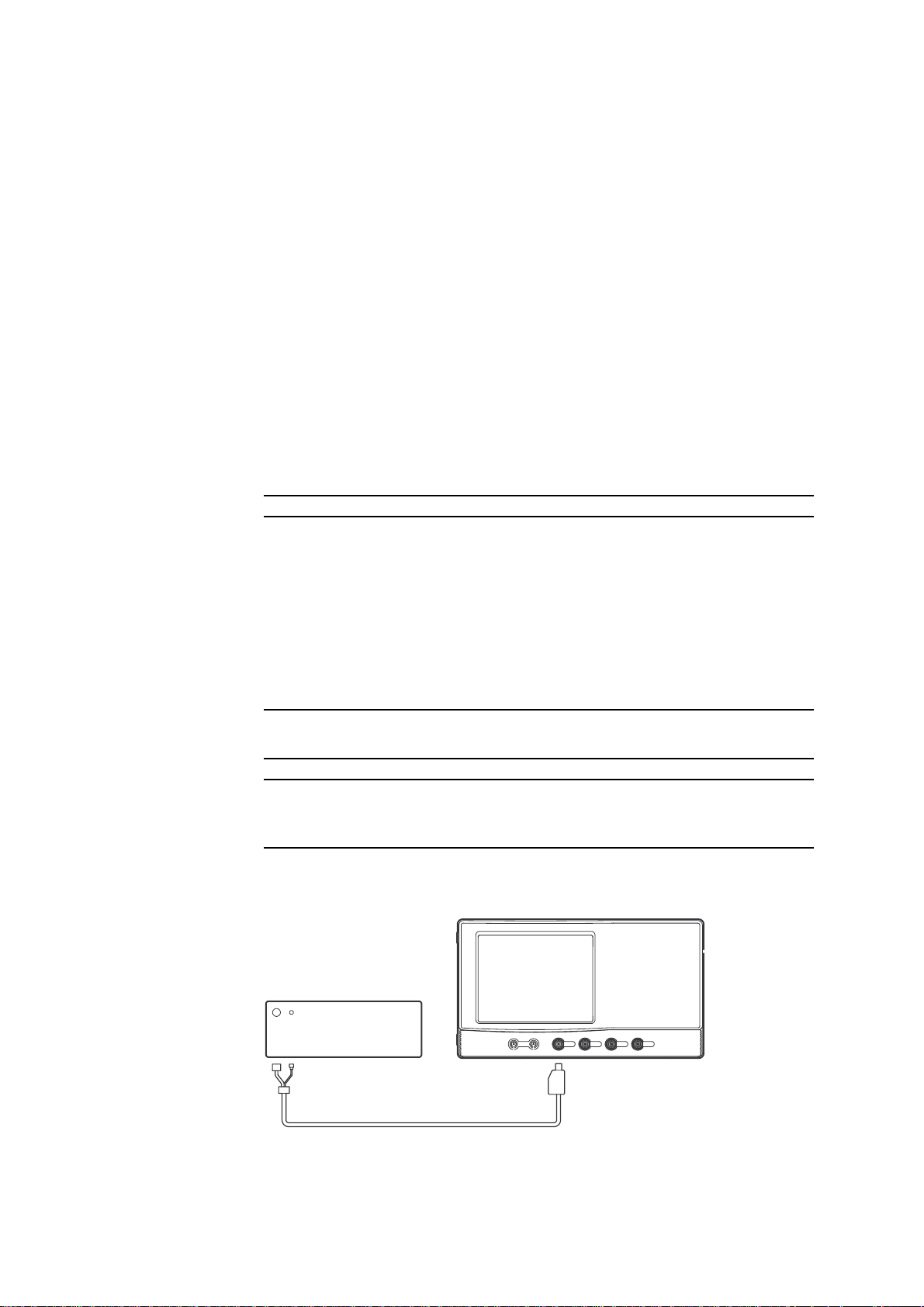
Connection
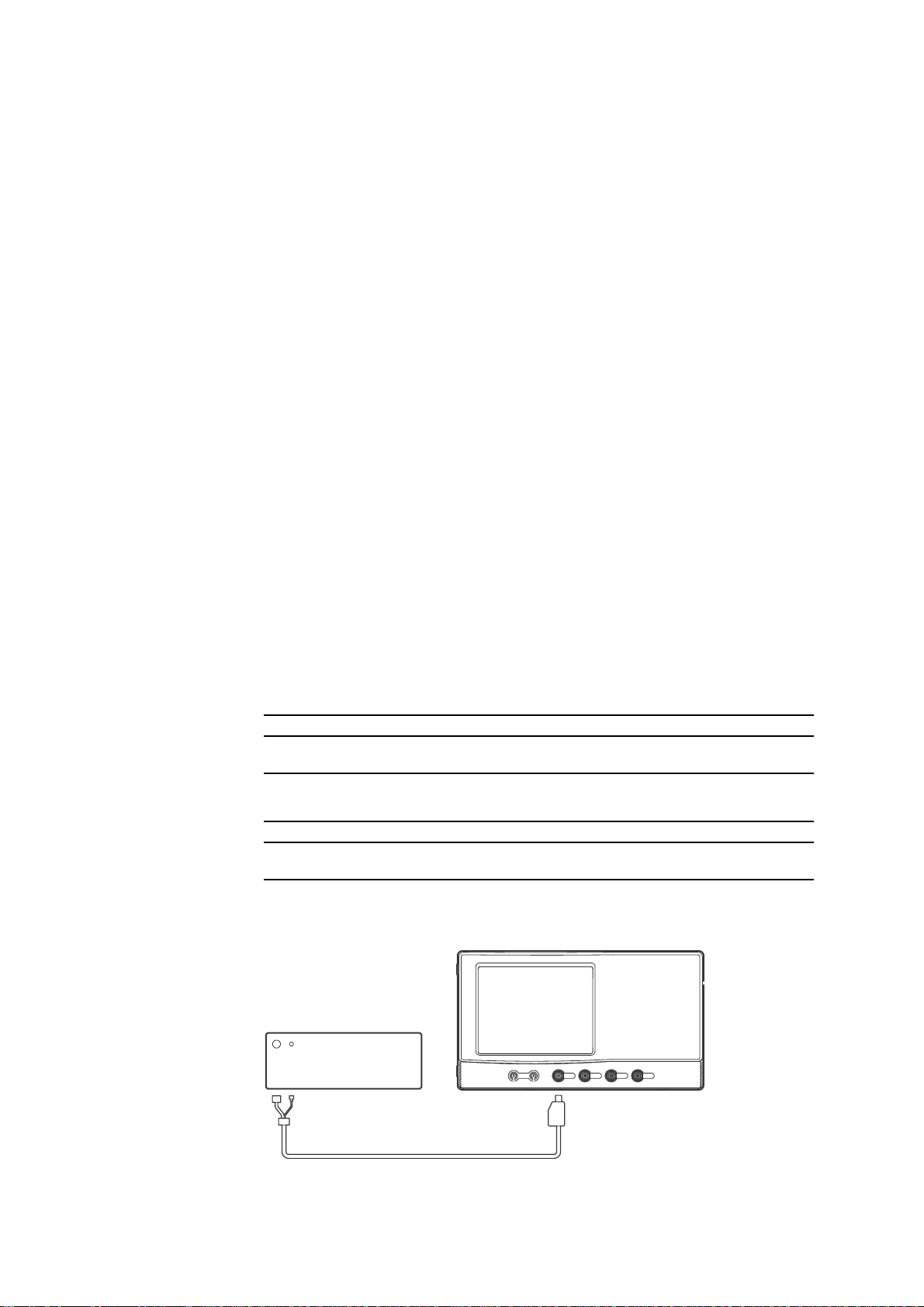
DL7100/DL7200
Calibrator
Programable Head
SM 701410-01E2 - 2
Page 10

2.4 Self diagnosis
Procedure
1) Turn on the power source of the DL7100/DL7200. After warm-up press the MISC key,
followed by Calibration soft key, then press the Cal Exec soft key to calibrate the
instrument.
Next, press the INITIALIZE key, then press the Initialize soft key to initialize the
settings.
2) Set the DL7100/DL7200 oscilloscope as shown below.
VERTICAL (for all channels)
Coupling DC1 MΩ
V/div According to the inspection item below
Probe 1:1
HORIZONTAL
T/div 1 ms/div
TRIGGER
Mode Auto
ACQ
Mode Box Average
Count Infinite
DISPLAY
Format Single
MEASURE
Mode ON
Item Set Up ▼ (Set to channel to be measured)
Select A vg.
Time Range 1 –5 div
Time Range 2 +5 div
2
PERFORMANCE TEST
3) Input the following voltages from the voltage generator to the DL7100/DL7200 to be
tested, read the indication on the DL7100/DL7200 (value of Avg), and compare the
reading with the tolerance.
Measurement Range Test input voltage Tolerance
2 mV/div –8, 0, +8 mV ±0.44 mV
5 mV/div –20, 0, +20 mV ±0.8 mV
10 mV/div –40, 0, +40 mV ±1.4 mV
20 mV/div –80, 0, +80 mV ±2.6 mV
50 mV/div –200, 0, +200 mV ±6.2 mV
100 mV/div –400, 0, +400 mV ±14 mV
200 mV/div –800, 0, +800 mV ±26 mV
500 mV/div –2, 0, +2 V ±62 mV
1 V/div –4, 0, +4 V ±140 mV
2 V/div –8, 0, +8 V ±260 mV
5 V/div –20, 0, +20 V ±620 mV
10 V/div –40, 0, +40 V ±1.22 V
4) Test all channels in the same manner.
SM 701410-01E
2 - 3
Page 11

2.6 Frequency Response Test
Specifications
DC50 Ω (1 V/div to 10 mV/div) DC to 500 MHz (–3 dB point)
DC50 Ω (2 mV/div and 5 mV/div) DC to 400 MHz (–3 dB point)
Permissible Range
Range Input Amplitude (p-p) Input Frequency Permissible Range (Sdev)
1 V/div 5 V 500 MHz 1.26 V to 1.98 V
200 mV/div 1.2 V 500 MHz 301 mV to 476 mV
50 mV/div 0.3 V 500 MHz 75.1 mV to 119 mV
5 mV/div 30 mV 400 MHz 7.51 mV to 11.9 mV
2 mV/div 12 mV 400 MHz 3.01 mV to 4.76 mV
Equipment Required
Equipment Qty Mandatory Specifications Recommended
Calibrator 1 Output voltage 0 V to 10 V WAVETEK 9500
Programmable Head 1 WAVETEK 9520
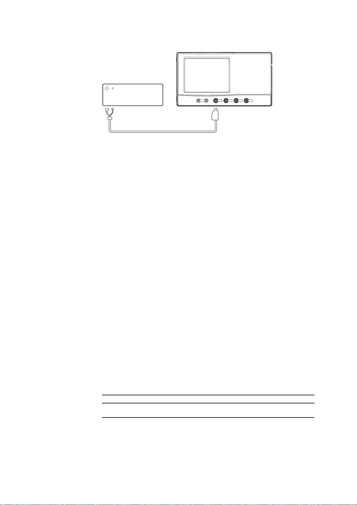
Connection
Output resolution 1 mV
Output frequency range 0.1 MHz to 500 MHz
DL7100/DL7200
Calibrator
Programable Head
Procedure
1) Turn on the power source of the DL7100/DL7200. After warm-up press the MISC key,
followed by Calibration soft key, then press the Cal Exec soft key to calibrate the
instrument.
Next, press the INITIALIZE key, then press the Initialize soft key to initialize the
settings.
2) Set the DL7100/DL7200 as shown below.
VERTICAL (for all channel)
Coupling DC50 Ω
V/div Set this according to following measurement
conditions
Probe 1:1
HORIZONTAL
T/div 2 ns/div
TRIGGER SIMPLE
Mode Normal
SIMPLE
SM 701410-01E2 - 4
Page 12

2.6 Frequency Response Test
Source (Channel to be tested)
ACQ
Mode Average
Count Infinite
Weight 4
Record Length 1 k
DISPLAY
Format Single
MEASURE
Mode ON
Item Set up ▼ (Set to channel to be tested)
Select Sdev
Time Range 1 –5.00 div
Time Range 2 +5.00 div
3) Input voltages as listed on the following table to the DL7100/DL7200 you are testing,
and check if the automatically measured value of waveform parameters (Sdev) is within
the permissible range.
2
PERFORMANCE TEST
Range Input Amplitude (p-p) Input Frequency Permissible Range (Sdev)
1 V/div 5 V 500 MHz 1.26 V to 1.98 V
200 mV/div 1.2 V 500 MHz 301 mV to 476 mV
50 mV/div 0.3 V 500 MHz 75.1 mV to 119 mV
5 mV/div 30 mV 400 MHz 7.51 mV to 11.9 mV
2 mV/div 12 mV 400 MHz 3.01 mV to 4.76 mV
4) Test all channels in the same manner.
2.7 Time-Base Accuracy Test
Specifications
±0.005%
Permissible Range
Time Range Input Frequency Permissible Range
2 µs/div 500.2 MHz 200±25 kHz
5 µs/div 200.1 MHz 100±10 kHz
Equipment Required
Equipment Qty Mandatory Specifications Recommended
Calibrator 1 300mVp-p, sine wave WAVETEK 9500
Programmable Head 1 WAVETEK 9520
200.1MHz and 500.2MHz
SM 701410-01E
2 - 5
Page 13
Connection
DL7100/DL7200
Calibrator
Programable Head
Procedure
1) Turn on the power source of the DL7100/DL7200. After warm-up press the MISC key,
followed by Calibration soft key, then press the Cal Exec soft key to calibrate the
instrument.
Next, press the INITIALIZE key, then press the Initialize soft key to initialize the
settings.
2) Set the DL7100/DL7200 as shown below.
VERTICAL
CH1
V/div 50 mV/div
Coupling DC50 Ω
Probe 1:1
HORIZONTAL
T/div According to the inspection item below
Display
Format Single
ACQ
Record Length 10k
MEASURE
Mode ON
Item Set up ▼
CH1 Select Freq
3) Input a 300 mVp-p sine wave signal with the input frequency listed in the table below to
the DL7100/DL7200 you are testing, and check if the automatically measured waveform parameters (Freq) are within the permissible range.
Time Range Input Frequency Permissible Range (Freq)
2 µs/div 500.2 MHz 200±25 kHz
5 µs/div 200.1 MHz 100±10 kHz
SM 701410-01E2 - 6
Page 14
2.8 Trigger Sensitivity Test
Specifications
DC to 500 MHz: 1 divp-p on the screen
2.8 Trigger Sensitivity Test
Permissible Range
500 mV/div 500 MHz 1 divp-p on the screen
Equipment Required
Equipment Qty Mandatory Specifications Recommended
Calibrator 1 500 mVp-p, 500 MHz, sine wave WAVETEK 9500
Programmable Head 1 WAVETEK 9520
Connection
DL7100/DL7200
Calibrator
Programable Head
2
PERFORMANCE TEST
Procedure
1) Turn on the power source of the DL7100/DL7200. After warm-up press the MISC key,
followed by Calibration soft key, then press the Cal Exec soft key to calibrate the
instrument.
Next, press the INITIALIZE key, then press the Initialize soft key to initialize the
settings.
2) Set the DL7100/DL7200 as shown below.
VERTICAL (for all channels)
V/div 500 mV/div
Coupling DC50 Ω
Probe 1:1
HORIZONTAL
T/div 1ns/div
TRIGGER
Mode Normal
ENHANCED
Type Pattern
Set Pattern ▼
Clock CH (Set to channel to be measured)
Slope ↑ (channel to be measured)
X (the other channel)
SM 701410-01E
2 - 7
Page 15
Condition True
Level / Coupling ▼
Level 0 mV
Coupling DC
DISPLAY
Format Single
ACQ
Record Length 1 k
Mode Average
Count Infinite
Weight 4
3) Input a sine wave signal of 500 mVp-p 500 MHz to the DL7100/DL7200, and confirm
that the waveform stabilizes.
NOTE If the trigger is not activated, adjust the trigger lever within ±250 mV until the trigger is
activated.
4) Test all channels in the same manner.
2.9 Trigger Accuracy Test
Specifications
±(1 div.+10% of the trigger level)
Permissible Range (when 200 mV/div)
Trigger level Offset Permissible Range
600 mV 600 mV –260 mV ≤ (Vin + Vout) / 2 ≤ 260 mV
–600 mV –600 mV –260 mV ≤ (Vin + Vout) / 2 ≤ 260 mV
Equipment Required
Equipment Qty Mandatory Specifications Recommended
Calibrator 1 400mVp-p, 2kHz, sine wave WAVETEK 9500
Programmable head 1 WAVETEK 9520
Connection
Calibrator
DL7100/DL7200
Programable Head
SM 701410-01E2 - 8
Page 16

2.9 Trigger Accuracy Test
Procedure
1) Turn on the power source of the DL7100/DL7200. After warm-up press the MISC key,
followed by Calibration soft key, then press the Cal Exec soft key to calibrate the
instrument.
Next, press the INITIALIZE key, then press the Initialize soft key to initialize the
settings.
2) Set the DL7100/DL7200 oscilloscope as follows.
VERTICAL (for all channels)
V/div 200 mV/div
Probe 1:1
Band Width 20 MHz
Offset –600 mV, 600 mV
HORIZONTAL
T/div 100 µs/div
TRIGGER
ENHANCED
Type OR
Window ON
Set Pattern ▼
IN, OUT (channel to be measured)
– (the other channel)
Level / Coupling ▼
Center –600 mV, 600 mV
Width 1.2 V
DISPLAY
Format Single
CURSOR
Type Marker
Position 0.0 div
2
PERFORMANCE TEST
SM 701410-01E
3) Input a sine wave signal of 400 mVp-p, 2 kHz to the DL7100/DL7200 oscilloscope, and
use cursors to read the voltage of the waveform at the trigger position. Set Vin for
Polarity IN, Vout for Polarity out, and check if (Vin+Vout)/2 is within the permissible
range.
Trigger level Offset Permissible Range
600 mV 600 mV –260 mV ≤ (Vin + Vout) / 2 ≤ 260mV
–600 mV –600 mV –260 mV ≤ (Vin + Vout) / 2 ≤ 260mV
4) Test all channels in the same manner.
2 - 9
Page 17

2.10 Logic Input Function Test
Equipment Required
Equipment Qty Mandatory Specifications Recommended
Probe 1 400 MHz frequency range Yokogawa 700988
Logic Probe 2 8 bit Yokogawa 700985
Connection
DL7100/DL7200
GND (Black)
Input (Red)
Procedure
1) Turn on the power of the DL7100/DL7200 and press the INITIALIZE key, then press
the Initialize soft key to initialize the settings.
2) Press the AUTO SETUP key and select the Auto Setup soft key.
3) Press the LOGIC key, press the Mode function key, then select the ON.
4) Press the Select function key and select the Pod A soft key.
5) Press the Level function key, select the User soft key, and turn the jog shuttle to 0.5V.
6) Set POD B in the same manner as POD A.
7) Press the ENHANCED key, press the Type function key, and select the Logic soft key.
8) Press the Set Pattern function key, set the Clock CH to None and set Condition to
Enter.
9) Set the 1st bit status of POD A to H. The other bits and the bits of the other POD are set
to X.
10) Connect the 1st bit probe of POD A to the PROBE COMPENSATION output terminal.
11) Check whether the trigger activated correctly. If the logic input signal is displayed,
check the waveform on the screen.
12) Change the connection of the probe and test the other bits in the same manner.
13) Change the connection of POD B and test POD B in the same manner.
SM 701410-01E2 - 10
Page 18

Chapter 3 ADJUSTMENTS
Contents of This Chapter
3.1 Introduction
3.2 Test Environment
3.3 Equipment Required
3.4 DC Gain Adjustment on the AD board
3.5 Flatness Adjustment on the Analog board
3.1 Introduction
The main unit cover must be removed before adjusting the DL7100/DL7200 read the
warning and caution below before doing so.
3.1 Introduction
3
ADJUSTMENTS
WARNING
CAUTION
Circuit patterns of the printed circuit board are exposed. Be careful when handling so
that hands or fingers are not injured by the protruding pins.
• Circuit patterns of the printed circuit board are exposed. If these patterns touch other
metallic materials, electrical shorting will occur, causing the circuit to be damaged or
burnt.
• It is sometimes necessary to turn the DL7100/DL7200 upside down for adjustment. Do
not drop, or allow the instrument to fall over.
•When feeding power with the DL7100/DL7200’s cover open, apply a flow of air to the
AD board.
3.2 Test Environment
1) Operate the instrument under the following conditions.
• Ambient temperature: 23 ±2 ˚C
• Humidity: 55 ±10 % RH
•Voltage of power supply: Specified voltage ±1 %
• Frequency of power supply: Specified frequency ±1 %
SM 701410-01E
2) Warm up time
•More than 30 minutes after tuning ON the instrument.
• Confirm that self calibration is correctly executed after a 30 minute warm up.
(Be sure to pay attention to the warm up time of all equipment that will be used in the
test.)
3 - 1
Page 19

3.3 Equipment Required
Table 3.1 Equipment required
Equipment Critical Specification Recommended
Calibrator DC WAVETEK 9500
Programmable Head Output Level : 1 V WAVETEK 9520
Accuracy : < 0.02%
Square wave
Frequency : 10 kHz
Output Level : > 60 Vp-p
NOTE The values shown in the specification column are those set in this service manual.
These values do not indicate the performances of the recommended equipment and
tools. Therefore, non-designated equipment and tools which satisfy the specifications
may be permitted for use.
3.4 DC Gain Adjustment on the AD board
Procedure
1) Remove the main unit cover.
2) Allow the unit to warm up for 10 minutes or more.
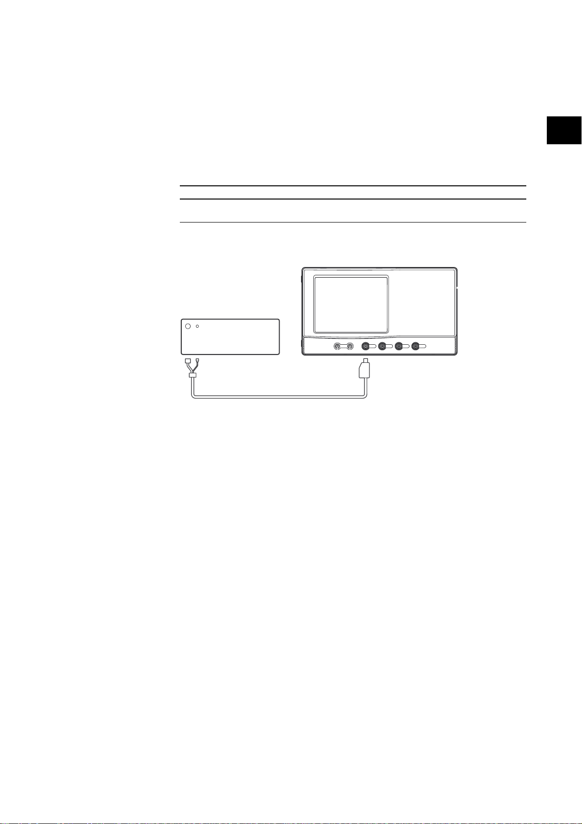
3) Connect each instrument as shown in Figure 3.1 Connection method.
DL7100/DL7200
Calibrator
Programable Head
Figure 3.1 Connection Method
4) Press the INITIALIZE key and select the Initialize soft key to execute initialization.
5) Press the MISC key and select the Calibration soft key.
6) Press the Cal Exec soft key to perform calibration.
3 - 2 SM 701410-01E
Page 20

3.4 DC Gain Adjustment on the AD board
7) Set up the DL7100/DL7200 and calibrator as follows.
DL7100/DL7200 VERTICAL (for all channels)
V/div 2 mV/div
Position 0 div
Probe 1:1
Offset +1.000 V
Bandwidth 20 MHz
HORIZONTAL
T/div 1 ms/div
TRIGGER
Mode Auto
ACQ
Mode Box Average
Count Infinite
DISPLAY
Format Single
MEASURE
Mode ON
Item Set Up ▼(Set to channel to be measured)
Select A vg.
Time Range 1 -5 div
Time Range 2 +5 div
Calibrator DC Output Level +1.0000 V
3
ADJUSTMENTS
8) Adjust the variable resistor (refer to table 3.2, “ Adjustment Point” and figure 3.2,3.3,
“Adjustment Point Location Diagram”) corresponding to each channel so that the DC
wave form fits within 1 V±1 mV as shown in figure 3.4, “Observed Waveform.”
9) Perform the adjustment of 7) for all channels.
Table 3.2 Adjustment Point
Channel Adjustment Point
ch1 R707
ch2 R714
ch3 R721
ch4 R728
SM 701410-01E
3 - 3
Page 21

R707
R714
R721
R728
Figure 3.2 Adjustment Point Location Diagram (DL7100)
3 - 4 SM 701410-01E
Page 22

3.4 DC Gain Adjustment on the AD board
R707
R714
R721
R728
3
ADJUSTMENTS
Figure 3.3 Adjustment Point Location Diagram (DL7200)
SM 701410-01E
3 - 5
Page 23

Figure 3.4 Observed Waveform
3.5 Flatness Adjustment on the Analog Board
NOTE Before performing this flatness adjustment, the DC gain adjustment on the AD board
must have been completed.
Procedure
1) Remove the main unit cover.
2) Turn on the power and allow the unit to warm up for 10 minuets or more.
3) Connect each instrument as shown in figure 3.5, “Connection Method.”
DL7100/DL7200
Calibrator
Programable Head
Figure 3.5 Connection Method
4) Press the INITIALIZE key and select the Initialize soft key to execute initialization.
5) Press the MISC key and select the Calibration soft key.
6) Select the Cal Exec soft key to perform calibration.
3 - 6 SM 701410-01E
Page 24

3.5 Flatness Adjustment on the Analog board
7) For adjustment of the /10 range, set up the DL7100/DL7200 oscilloscope and calibrator
as follows.
DL7100/DL7200 VERTICAL (for all channels)
V/div 100 mV/div
Position 0 div
Probe 1:1
HORIZONTAL
T/div 10 µs/div
TRIGGER
Mode Auto
ACQ
Mode Box Average
Count Infinite
DISPLAY
Format Single
Calibrator Wave Form Square wave
Frequency 10 kHz
Amplitude 600 mVp-p
8) Adjust the variable capacitors CV101 and CV201, (refer to figure 3.6, “Adjustment
Point Location Diagram”) so that the top of the waveform becomes flat as shown in
figure 3.7, “Observed Waveform.” The flatness of the waveform must be fitted within
±0.1 div.
9) For adjustment of the /100 range, set up the DL7100/DL7200 oscilloscope and calibrator as follows.
DL7100/DL7200 VERTICAL (for all channels)
V/div 1 V/div
Position 0 div
Probe 1:1
HORIZONTAL
T/div 10 µs/div
TRIGGER
Mode Auto
ACQ
Mode Box Average
Count Infinite
DISPLAY
Format Single
Calibrator Wave Form Square wave
Frequency 10 kHz
Amplitude 6 Vp-p
10) Adjust the variable capacitors CV102 and CV202 (refer to figure 3.6, “Adjustment
Point Location Diagram”) so that the top of the waveform becomes flat as shown in
figure 3.7, “Observed Waveform.” The flatness of the waveform must be fitted within
±0.1 div.
3
ADJUSTMENTS
SM 701410-01E
3 - 7
Page 25

11)For adjustment of the /200 range, set up the DL7100/DL7200 oscilloscope and calibrator as follows.
DL7100/DL7200 VERTICAL (for all channels)
V/div 10 V/div
Position 0 div
Probe 1:1
HORIZONTAL
T/div 10 µs/div
TRIGGER
Mode Auto
ACQ
Mode Box Average
Count Infinite
DISPLAY
Format Single
Calibrator Wave Form Square wave
Frequency 10 kHz
Amplitude 60 Vp-p
12)Adjust the variable capacitors CV103 and CV203 (refer to figure 3.6, “Adjustment
Point Location Diagram” ) so that the top of the waveform becomes flat as shown in
figure 3.7, “Observed Waveform.” The flatness of the waveform must be come within
±0.1 div.
CV202
The assembly number differs dependeing on
the date of manufacture as follows:
During or before July, 2001: B9969MA
July, 2001 – December, 2001: B9989MA
After December, 2001: B9989ML
CV203
CV103
CV102
CV101
CV201
Figure 3.6 Adjustment Point Location Diagram
3 - 8 SM 701410-01E
Page 26

Figure 3.7 Observed Waveform
3
ADJUSTMENTS
SM 701410-01E
3 - 9
Page 27

4.1 Introduction
Chapter 4 PRINCIPLES OF OPERATION
Contents of This Chapter
4.1 Introduction
4.2 Function of each assembly
4.3 Function of Each ASIC
4.1 Introduction
The block diagrams of the DL7100 are shown in figure 4.1 and figure 4.2.
The block diagrams of the DL7200 are shown in figure 4.3 and figure 4.4.
Figure 4.1 and figure 4.3 are block diagrams of the circuit from the analog input to the
data acquisition circuit including the attenuator, one-chip amplifier, analog multiplexer,
A/D converter, trigger comparator, trigger circuit, and the ring buffer memory and its
controller.
Figure 4.2 and figure 4.4 are block diagrams of (1) the data processing section which
processes the acquired data and displays the waveform, (2) the CPU, and (3) the
peripheral circuitry. In addition, figure 4.2 and figure 4.4 include a block diagram of the
logic input circuit.
4
PRINCIPLE OF THE OPERATION
4.2 Function of Each Assembly
This section describes the ATT board assembly and AFC board assembly.
(1) Analog Board Assembly
The analog board assembly has a coupling switch for AC/DC, 1 MΩ/50 Ω, and GND/
Measure and a switch circuit for the attenuator (1:1/10:1/100:1/200:1). Relays are used
to make the switch. In addition, a one-chip amplifier IC and an analog multiplexer IC
are onboard.
The one-chip amplifier IC has a gain switch circuit, a low-pass filter circuit (external
capacitor), a trigger coupling circuit (external capacitor), and a trigger bandwidth
limiting circuit (external capacitor). In addition, the input offset voltage and the trigger
level are varied using an external DC voltage input. The frequency bandwidth of the IC
is approximately 600 MHz.
As indicated in figure 4.1, the vertical sensitivity from 10 V/div to 2 mV/div is achieved
by switching the gain on the attenuator and the one-chip amplifier IC.
The analog multiplexer IC is used to achieve the interleave operation.
During the interleave operation, the input signal of CH1 (CH3) is supplied to the A/D
converter of CH2 (CH4).
The frequency bandwidth of the IC is approximately 2 GHz.
SM 701410-01E
The above-mentioned control signal, offset, and DC voltage for the trigger level are
supplied by the analog front-end controller (AFC) on the AD board assembly.
4 - 1
Page 28

Table 4.1 Setting Range and Amplifying Level
Setting Range Attenuator Division Ratio Amplifying Rate
2 mV/div 1/1 x25
5 mV/div 1/1 x10
10 mV/div 1/1 x5
20 mV/div 1/1 x2.5
50 mV/div 1/1 x1
100 mV/div 1/10 x5
200 mV/div 1/10 x2.5
500 mV/div 1/10 x1
1 V/div 1/100 x5
2 V/div 1/100 x2.5
5 V/div 1/100 x1
10 V/div 1/200 x1
The setting range here is for the 1:1 probe setting.
(2) AD Board Assembly
The AD board assembly has the time base, trigger, A/D converter, ring buffer controller
(RBC), and analog control circuits onboard.
The time base is of a PLL configuration. 1 GHz and 800 MHz can be switched. On the
DL7100, the frequency of the clock is converted to 500 MHz or 400 MHz using highspeed ECL logic and distributed to each channel. When in interleave mode, the clock
for CH2 and CH4 is delayed by 1 ns with respect to the clock for CH1 and CH3,
respectively. On the DL7200, the 1-GHz or 800-MHz clock is distributed to each
channel without any frequency conversion. When in interleave mode, the clock for
CH2 and CH4 is delayed by 500 ps with respect to the clock for CH1 and CH3, respectively. For making minute time measurements of phase difference between the trigger
and sampling clock (needed during repetitive sampling mode, for example), the T-V
converter (TVC) is used.
The trigger section consists of a comparator, fast trigger logic (FTL), and pulse width
detector (PWD). It also has a TV trigger circuit used only on CH1. The comparator has
a window comparator function that allows window triggering. The window width is
controlled by an external DC voltage input. The frequency bandwidth of the comparator IC is 1 GHz.
On the DL7100, the A/D converter operates at 500 MHz only when the sampling rate is
500 MS/s or when in 1 GS/s interleave mode. In all other cases, the A/D converter
operates at 400 MHz. Sampling rates of 200 MS/s or lower are attained by extracting a
portion of the data sampled at 400 MHz using the RBC. On the DL7200, the A/D
converter operates at 1 GHz only when the sampling rate is 500 MS/s or 1 GS/s or when
in 2 GS/s interleave mode. In all other cases, the A/D converter operates at 800 MHz.
A sampling rate of 500 MS/s is attained by extracting a portion of the data sampled at 1
GHz using the RBC. Sampling rates of 200 MS/s or lower are attained by extracting a
portion of the data sampled at 800 MHz using the RBC.
The RBC performs primary processing such as the above-mentioned data extraction of
sampled data, envelope, and box averaging, then stores the data in the ring buffer
memory. The written data are transferred to the acquisition memory interface (AMI) on
the CPU board assembly according to the trigger address.
4 - 2
The analog control circuit consists of an analog front-end controller (AFC), a PWM D/
A converter, and a serial/parallel converter. This circuit controls the analog section of
the analog board assembly and the AD board assembly.
SM 701410-01E
Page 29

4.2 Function of each assembly
(3) Ring Buffer Memory Board Assembly
The ring buffer memory board assembly consists of a fast bus buffer (FBB) and ring
buffer memory (fast SRAM).
The 701410 and 701420 use a 1-Mbit SRAM and a 4-Mbit SRAM, respectively.
The 701430 and 701440 have twice the amount of SRAM that the 701410 and 701420
have, respectively.
(4) CPU Board Assembly
The CPU board assembly consists of the secondary data processing section, a display
section (for displaying waveforms and other information), the CPU, and its peripheral
circuits.
The secondary data processing section consists of an acquisition memory interface
(AMI), work memory (PBSRAM), and the acquisition memory on the ACQ memory
board assembly. The AMI processes the data (averaging, for example) that are transferred from the RBC on the AD board assembly and stores the result in the acquisition
memory. Then, the AMI converts the stored data to display data by performing additional processing such as compression and interpolation. The resultant data are transferred to the graphic control process (GCP) according to the display update interval.
The AMI also has the computation function (addition, subtraction, multiplication,
division, differentiation, integration, etc.) and auxiliary functions such as automated
measurement of waveform parameters.
The display section consists of a GCP, graphic memory (synchronous GRAM), character memory (fast SRAM), and VGA VIDEO OUT circuits. The GCP writes the waveform data that are transferred from the AMI (includes the AMI on the logic board
assembly) to the graphic memory. It synthesizes the contents of the graphic memory
and the character memory and displays them on the TFT color LCD. The GCP also
controls the built-in printer.
The CPU is Hitachi's HD6417709A operating at 66 MHz. The CPU peripheral circuits
include the main memory (synchronous DRAM), flash memory, backup memory, a
GPIB controller, a SCSI controller, an FDD controller, a Centronics interface, and an
RS-232 interface. The CPU I/O interface (CIO) controls a part of these peripheral
circuits.
4
PRINCIPLE OF THE OPERATION
SM 701410-01E
(5) ACQ Memory Board Assembly
The ACQ memory board assembly has an acquisition memory (synchronous DRAM)
onboard. It is controlled by the acquisition memory interface (AMI) on the CPU board
assembly. The acquisition memory uses a 64-Mbit synchronous DRAM. The 701430 and
701440 uses twice the amount of 64-Mbit synchronous RAMs as the 701410 and 701420.
(6) Logic Board Assembly (Option)
The logic board assembly consists of an interface section of the logic probe, a data
acquisition section, and a logic trigger circuit. The interface section supplies power to
the logic probe and provides a buffer for the logic input. Similar to the analog input
section, the data acquisition section has an RBC, a ring buffer memory, an AMI,
acquisition memory, and a work memory. For the ring buffer memory, a 1-Mbit SRAM
is used for option /N1, /N3 and a 4-Mbit SRAM is used for option /N2, /N4.
Option /N3 and option /N4 use twice the amount of SRAM as option /N1 and option /
N2, respectively.
4 - 3
Page 30

(7) Rear Board Assembly
The rear board assembly provides EXT CLOCK IN/EXT TRIG IN/TRIG GATE IN and
TRIG OUT.
This board supplies the power source (+12V, -12V) for the active probes.
(8) Key Board Assembly
Key switches, LEDs, the rotary encoder, and the jog shuttle are installed on the key
board assembly.
(9) Line Trigger Board Assembly
The AC Line input from the inlet is supplied to the power supply unit across the switch
on the line trigger board assembly.
This assembly also contains the line trigger circuit.
(10) Power Board Assembly
The power board assembly distributes the DC voltage output from the power supply
unit to the AD board assembly, ring buffer memory board assembly, and CPU board
assembly.
(11) Bus Board Assembly
The CPU board assembly and the AD board assembly exchange signals via the bus
board assembly.
(12) LCD Board Assembly
The LCD board assembly converts the connector of the LCD signal cable.
(13) LCD Assembly
8.4-inch color TFT LC display
Full display resolution: 640 x 480
Waveform display resolution: 500 x 384
(14) Printer Assembly (Option)
The printer is of a thermal sensitivity type that prints 8 dots per mm and 832 dots per
line. A hardcopy of the display is printed in approximately 12 seconds.
(15) FDD Assembly
The FDD assembly supports 3.5-inch floppy disks with the formats of 640 KB, 720 KB,
1.2 MB, and 1.44 MB.
(16) Ethernet + PC Card Interface Board Assembly (option)
Option /C9 consists of a PC card interface section. Option /C10 consists of a PC card
interface section and an Ethernet interface section. The PC card interface section has a
PC card slot and a PC card controller. The Ethernet interface section has an Ethernet
connector and a LAN (local area network) controller. These interfaces are controlled by
the CPU and CPU I/O interface (CIO) that are on the CPU board assembly.
4 - 4
(17) OPT TRIG Board Assembly (option)
Option /F7 consists of a CANBus Trigger section. The OPT TRIG Board Assembly
provide CANBus Trigger signal.
SM 701410-01E
Page 31

4.3 Function of Each ASIC
The following items describe the IC and the gate array function used in each assembly.
(1) Analog Front-End Controller (AFC)
The AFC is a Bi-CMOS gate array. Its main functions are controlling the analog frontend circuit and assisting the trigger circuit. It has a PWM signal output circuit used for
D/A conversion, a parallel port, a serial port, a trigger hold-off circuit, an auto trigger
circuit, a TV trigger generator, a fast counter, and a slow counter, etc.
(2) Fast Trigger Logic (FTL)
The FTL is an ECL gate array. Its main functions include generation of trigger signals
according to the trigger functions, trigger hold-off function, and the control of the timeto-voltage converter (TVC).
(3) Pulse Width Detector (PWD)
The PWD is an analog IC. Using an internally-startable oscillator and an external
counter (AFC), it detects the pulse width for width triggering.
(4) Time-to-Voltage Converter (TVC)
This is the analog IC that measures the internal sampling clock and trigger time, and
coverts time to voltage.
4.3 Function of Each ASIC
4
PRINCIPLE OF THE OPERATION
(5) Ring Buffer Memory Controller (RBC)
The RBC is a Bi-CMOS gate array. It performs primary processing of the data such as
the extraction of the sampled data, envelope, and box averaging. It also provides
functions for controlling the ring buffer memory and the interface to the acquisition
memory interface (AMI).
(6) Fast Bus Buffer (FBB)
The FBB is a CMOS gate array. Its function is to provide a buffer for the data bus,
address bus, and control signal between the ring buffer memory controller (RBC) and
the ring buffer memory.
(7) Acquisition Memory Interface (AMI)
The AMI is a CMOS gate array. Its functions include interface to the ring buffer
memory controller (RBC), interface to the graphic control processor (GCP), averaging,
history control, waveform computation, and auxiliary functions for the automated
measurement of waveform parameters.
(8) Graphic Control Processor (GCP)
The GCP is a CMOS gate array. Its functions include interface to the acquisition
memory interface (AMI), graphic memory and character memory control, waveform
drawing function (accumulated display, for example), built-in printer control, and
display data generation for the LCD.
SM 701410-01E
(9) CPU I/O Interface (CIO)
The CIO is a CMOS gate array. Its functions include interface to the CPU
(HD6417709A) and the peripheral ICs, keyboard control, LED control, interrupt
control, and DMA selection.
(10) CANBus Trigger Logic (CTL)
The CTL is Field Programmable Gate array. Its function is generation of CANBus
trigger signal.
4 - 5
Page 32

CH1/CH2
SRAM
SRAM
CH3/CH4
SRAM
SRAM
Signal
Control
FBB
RBC
RBC
FBB
Board Assembly
Ring Buffer Memory
FTL
TVC
Assembly
To Rear Board
*
PWD
AFC
Time Base
Level Converter
AD Board Assembly
*
A/D Converter
To Logic Board
Assembly
Trigger Level
Offset
Filter
(20MHz
100MHz)
TV Trigger
*
Comparator
Line Trigger
*
Assembly
Assembly
From Logic Board
From Bus Board
Assembly
Assembly
To CPU Board
To AD Board
To Ring Buffer
*
*
*
DC
Memory Board Assembly
DC
DC
Analog Board Assembly
one chip Amplifier Multiplexer
Coupling
(GND/MES) ATT
Coupling
(1MΩ/50Ω)
(AC/DC)
Coupling
CH1
CH2
CH3
CH4
Figure 4.1 Block Diagram (Analog Section) of the DL7100
AC/DC
DC/AC/
HFrej
Gain1/1 1/10
1/100 1/200
GND/MES
1MΩ/50Ω
Power Board Assembly
DC
Unit
Power
AC
AC
Line T rigger Boar d Assembl y
4 - 6
SM 701410-01E
Page 33

(Option)
Printer
4.4 Functions of Each Gate Array
Key Board
Assembly
VGA Video OUT
LCD
GCP
CIO
Graphic
Memory
Memory
Character
FD Drive
FD Controller
CENTRONICS
GPIB
GPIB IF
Backup RAM
SCSI
SCSI IF
CENTRONICS IF
CPU
RS-232
RS-232 IF
DRAM
PC Card (/C9, /C10)
Flash ROM
Ethernet (/C10)
PC CARD IF Board
PC CARD IF
ETHERNET IF
Assembly (/C9)
or
Trigger Logic
*
To AD Board Assembly
Ethernet Board
Assembly (/C10)
LOGIC A
*
From AD Board
RBC
AMI
Assembly
FBB
SRAM
SRAM
Work
ACQ
LOGIC B
Memory
Memory
*
From AD Board
Assembly
4
PRINCIPLE OF THE OPERATION
Logic Board Assembly (Option)Rear Board Assembly
CPU Board Assembly
EXT CLOCK IN
EXT TRIG IN
TRIG GATE IN
TRIG OUT
PROBE POWER
From AD Board
x4
*
Assembly
AMI
Work Memory
BUS Board
Assembly
ACQ Memory
ACQ Memory
ACQ Memory
Board Assembly
CH1/CH2
AMI
CH3/CH4
Work Memory
*
To AD Board
Assembly
Signal
Control
Figure 4.2 Block Diagram (Digital Section) of the DL7100
SM 701410-01E
4 - 7
Page 34

CH1/CH2
SRAM
FBB
SRAM
SRAM
FBB
SRAM
CH3/CH4
SRAM
FBB
SRAM
SRAM
FBB
SRAM
Signal
Control
Board Assembly
Ring Buffer Memory
OPT TRIG Board
CTL
Assembly (/F7)
AD Board Assembly
Rate Reducer
A/D Converter
one chip Amplifier Multiplexer
RBC
RBC
RBC
RBC
Time Base
*
Assembly
To Logic Board
Trigger Level
Offset
AFC
TV Trigger
Filter
(20MHz
100MHz)
DC/AC/
HFrej
Gain1/1 1/10
1/100 1/200
PWD
Line Trigger
FTL
Comparator
Power Board Assembly
TVC
Assembly
To Rear Board
*
*
*
Assembly
Assembly
From Logic Board
From Bus Board
Assembly
Assembly
To CPU Board
To AD Board
To Ring Buffer
*
*
*
DC
DC
Power
Unit
AC
Memory Board Assembly
DC
DC
4 - 8
Analog Board Assembly
Coupling
(GND/MES) ATT
Coupling
(1MΩ/50Ω)
(AC/DC)
Coupling
CH1
CH2
CH3
CH4
Figure 4.3 Block Diagram (Analog Section) of the DL7200
AC/DC
GND/MES
1MΩ/50Ω
AC
Line T rigger Boar d Assembl y
SM 701410-01E
Page 35

(Option)
Printer
Key Board
Assembly
LCD
VGA Video OUT
GCP
CIO
Graphic
Memory
Memory
Character
FD Drive
FD Controller
CENTRONICS
GPIB
GPIB IF
Backup RAM
SCSI
SCSI IF
CENTRONICS IF
CPU
RS-232
RS-232 IF
DRAM
PC Card (/C9, /C10)
Flash ROM
Ethernet (/C10)
PC CARD IF Board
PC CARD IF
ETHERNET IF
Assembly (/C9)
or
Trigger Logic
*
To AD Board Assembly
Ethernet Board
Assembly (/C10)
LOGIC A
*
From AD Board
RBC
AMI
Assembly
FBB
SRAM
SRAM
Work
ACQ
LOGIC B
Memory
Memory
*
From AD Board
Assembly
RBC
FBB
SRAM
4
PRINCIPLE OF THE OPERATION
SRAM
Logic Board Assembly (Option)Rear Board Assembly
CPU Board Assembly
Work Memory
BUS Board
SM 701410-01E
EXT CLOCK IN
EXT TRIG IN
TRIG GATE IN
TRIG OUT
PROBE POWER
From AD Board
x4
*
Assembly
AMI
ACQ Memory
ACQ Memory
ACQ Memory
Board Assembly
Assembly
CH1/CH2
AMI
CH3/CH4
Work Memory
*
To AD Board
Assembly
Signal
Control
Figure 4.4 Block Diagram (Digital Section) of the DL7200
4 - 9
Page 36

Chapter 5 TROUBLESHOOTING
Contents of This Chapter
5.1 Introduction
5.2 Flowchart
5.3 Power Supply Secondary Voltage
5.4 Self Test
5.4.1 Key Board Test
5.4.2 Memory Test
5.4.3 FDD Test
5.4.4 SCSI Test
5.4.5 Printer Test
5.4.6 Accuracy Test
5.4.7 PC Card Test (Option)
5.1 Introduction
5
TROUBLESHOOTING
5.1 Introduction
WARNING
NOTE If an error message is displayed, the error may have been caused by incorrectly operat-
5.2 Flowchart
This chapter describes possible solutions for rectifying errors.
In such cases, assembly removal may be required.
Please keep the following precautions in mind.
Assembly replacement is to be performed only by qualified service technicians
who have experience working with the hazards involved (such as fire and
electrical shock).
ing the unit. Refer to the user’s manual, and perform the correct operation.
Figure 5.1, “Troubleshooting Flowchart” shows an analytical method for handling
malfunctions.
SM 701410-01E
5 - 1
Page 37

(1)
START
Power ON
LCD OK?
Check the
fuse
Fuse OK?
Check secondary
voltage of power supply
Voltage O K?
INITIALIZE
†
LCD OK?
*
Check secondary
voltage of power
supply unconnected
to power board
Voltage OK?
(1)’
Check each
board for shorts
Check display.
Connect RGB VIDEO
OUT to monitor
Replace
FUSE
*
Replace Power
Supply Unit or Line
Trig Board Ass’y
‡
No error
messages?
Execute self-test
Self-test
successful?
Execute performance
test.
Performance
test successful?
END
Maintenance Service is Required
Contact your nearest YOKOGAWA representative as listed on the back cover of this manual.
5 - 2
(2)’
Check error
contents.
(3)’
Check self-test
results
(4)’
Check
performance
test results.
Monitor
Replace CPU
display OK?
Check LCD
backlight
Backlight
Replace Lamp
lights up?
Replace LCD
* See section 5.3 for detailed instructions.
†
To initialize the settings, reboot the
DL7100/DL7200 while pressing the RESET
key.
‡
The monitor to be connected must be VGA
Figure 5.1 Troubleshooting Flowchart
Board Ass’y
Unit or
Inverter Unit
Ass’y
SM 701410-01E
Page 38

(1)’
5.2 Flowchart
A short may occur in an assembly other than the power supply unit.
To check in which voltage line a short has occurred, investigate each assembly to which
voltage is supplied, using a circuit tester.
Table 5.1, “Correspondence of Assembly to Voltage” shows the relationship between
assemblies and voltages supplied to them.
Table 5.1 Correspondence of Assembly to Voltage
Voltage Series Assembly No. Assembly
B9969MB AD Board Assembly (Model: 701410, 701420)
B9986MB AD Board Assembly (Model: 701430, 701440)
B9969MC CPU Board Assembly
B9969MD RB MEM2M Board Assembly (Model: 701410)
B9969ME RB MEM8M Board Assembly (Model: 701420)
B9986MD RB MEM4M Board Assembly (Model: 701430)
+3.3V B9969MF ACQ MEM Board Assembly (Model: 701410, 701420)
+5.0V B9969MK KEY Board Assembly
-5.2V B9969MH LOGIC2M Board Assembly (Option: /N1)
+12V B9969MP POWER Board Assembly
-12V B9969MH LOGIC2M Board Assembly (Option: /N1)
+24V B9969EA PRINTER Assembly (Option: /B5)
* The assembly number differs depending on the date of manufacture as follows:
During or before June, 2001: B9969MA
July, 2001 — December, 2001: B9989MA
After December, 2001: B9989ML
B9986ME RB MEM16M Board Assembly (Model: 701440)
B9986MF ACQ MEM Board Assembly (Model: 701430, 701440)
B9969MH LOGIC2M Board Assembly (Option: /N1)
B9969MJ LOGIC8M Board Assembly (Option: /N2)
B9986MH LOGIC4M Board Assembly (Option: /N3)
B9986MJ LOGIC16M Board Assembly (Option: /N4)
B9969MN PC Card I/F Board Assembly (Option: /C9)
B9986MG OPT TRIG Board Assembly (Option: /F7)
B9969MP POWER Board Assembly
B9969MQ LCD Board Assembly
B9969MT PC Card I/F + Ethernet Board Assembly (Option: /C10)
A1057VA LCD Unit
B9989ML
B9969MB AD Board Assembly (Model: 701410, 701420)
B9986MB AD Board Assembly (Model: 701430, 701440)
B9969MC CPU Board Assembly
B9969MH LOGIC2M Board Assembly (Option: /N1)
B9969MJ LOGIC8M Board Assembly (Option: /N2)
B9986MH LOGIC4M Board Assembly (Option: /N3)
B9986MJ LOGIC16M Board Assembly (Option: /N4)
B9969ML LINE TRG Board Assembly
B9969MN PC Card I/F Board Assembly (Option: /C9)
B9986MG OPT TRIG Board Assembly (Option: /F7)
B9969MP POWER Board Assembly
B9969MR REAR Board Assembly
B9969MT PC Card I/F + Ethernet Board Assembly (Option: /C10)
B9969EA PRINTER Assembly (Option: /B5)
A1092UN FDD Unit
B9989ML
B9969MB AD Board Assembly (Model: 701410, 701420)
B9986MB AD Board Assembly (Model: 701430, 701440)
B9969MC CPU Board Assembly
B9969MJ LOGIC8M Board Assembly (Option: /N2)
B9986MH LOGIC4M Board Assembly (Option: /N3)
B9986MJ LOGIC16M Board Assembly (Option: /N4)
B9969MP POWER Board Assembly
B9969MR REAR Board Assembly
B9969MB AD Board Assembly (Model: 701410, 701420)
B9986MB AD Board Assembly (Model: 701430, 701440)
B9969MC CPU Board Assembly
B9969MR REAR Board Assembly
A1476UP INVERTER Unit
B9969MB AD Board Assembly (Model: 701410, 701420)
B9986MB AD Board Assembly (Model: 701430, 701440)
B9969MJ LOGIC8M Board Assembly (Option: /N2)
B9986MH LOGIC4M Board Assembly (Option: /N3)
B9986MJ LOGIC16M Board Assembly (Option: /N4)
B9969MR REAR Board Assembly
B9969MC CPU Board Assembly
B9969SA FAN Assembly
*
*
ANALOG Board Assembly
ANALOG Board Assembly
5
TROUBLESHOOTING
SM 701410-01E
5 - 3
Page 39

(2)
When trouble occurs, refer to the instruction manual to determine whether the trouble
was caused by erroneous operation or by a hardware defect. Table 5.2, “Correspondence of Messages to Defective Assemblies,” shows which a trouble may be due to a
hardware failure.
Table 5.2 Correspondence of Massages to Defective Assemblies
Code Message Assembly No. Assembly
713 Calibration failure. ••• B9989ML
B9969MB AD Board Assembly (Model: 701410, 701420)
B9986MB AD Board Assembly (Model: 701430, 701440)
B9969MC CPU Board Assembly
B9969MD RB MEM2M Board Assembly (Model: 701410)
B9969ME RB MEM8M Board Assembly (Model: 701420)
B9986MD RB MEM4M Board Assembly (Model: 701430)
B9986ME RB MEM16M Board Assembly (Model: 701440)
B9969MF ACQ MEM Board Assembly
B9986MF ACQ MEM Board Assembly
B9969MM BUS Board Assembly
901 Failed to backup setup data. ••• B9969MC CPU Board Assembly
906 Fan stopped ••• B9969SA FAN Assembly
907 Backup battery is flat. B9969MC CPU Board Assembly
* The assembly number differs depending on the date of manufacture as follows:
During or before June, 2001: B9969MA
July, 2001 — December, 2001: B9989MA
After December, 2001: B9989ML
*
ANALOG Board Assembly
(Model: 701410, 701420)
(Model: 701430, 701440)
(3)
When trouble occurs, check the test item displaying FAIL and select the relevant
defective item from table 5.3, “Correspondence of Test Items to Defective Assemblies.”
If necessary, replace the relevant assembly.
Table 5.3 Correspondence of Test Item to Defective Assemblies
Test item Assembly No. Assembly
Key Board B9969MC CPU Board Assembly
Memory B9969MC CPU Board Assembly
FDD B9969MC CPU Board Assembly
SCSI B9969MC CPU Board Assembly
Printer B9969MC CPU Board Assembly
Accuracy B9989ML
PC Card B9969MC CPU Board Assembly
* The assembly number differs depending on the date of manufacture as follows:
During or before June, 2001: B9969MA
July, 2001 — December, 2001: B9989MA
After December, 2001: B9989ML
B9969MK KEY Board Assembly
A1092UN FDD Unit
B9969EA PRINTER Assembly (Option: /B5)
B9969MB AD Board Assembly (Model: 701410, 701420)
B9986MB AD Board Assembly (Model: 701430, 701440)
B9969MC CPU Board Assembly
B9969MD RB MEM2M Board Assembly (Model: 701410)
B9969ME RB MEM8M Board Assembly (Model: 701420)
B9986MD RB MEM4M Board Assembly (Model: 701430)
B9986ME RB MEM16M Board Assembly (Model: 701440)
B9969MF ACQ MEM Board Assembly (Model: 701410, 701420)
B9986MF ACQ MEM Board Assembly (Model: 701430, 701440)
B9969MM BUS Board Assembly
B9969MN PC Card I/F Board Assembly (Option: /C9)
B9969MT PC Card I/F + Ethernet Board Assembly (Option: /C10)
*
ANALOG Board Assembly
5 - 4
SM 701410-01E
Page 40

(4)
5.2 Flowchart
When trouble occurs, check the non-conforming test and select the relevant defective
assembly from table 5.4, “Correspondence of Test Items to Defective Assemblies.” If
necessary, replace the relevant assembly.
Table 5.4 Correspondence of Test Item to Defective Assemblies
Test item Assembly No. Assembly
2.5 Vertical Axis DC Voltage Accuracy B9989ML
Test B9969MB AD Board Assembly (Model: 701410, 701420)
B9986MB AD Board Assembly (Model: 701430, 701440)
2.6 Frequency Response Test B9989ML
B9969MB AD Board Assembly (Model: 701410, 701420)
B9986MB AD Board Assembly (Model: 701430, 701440)
2.7 Time-base Accuracy Test B9989ML
B9969MB AD Board Assembly (Model: 701410, 701420)
B9986MB AD Board Assembly (Model: 701430, 701440)
2.8 Trigger Sensitivity Test B9989ML
B9969MB AD Board Assembly (Model: 701410, 701420)
B9986MB AD Board Assembly (Model: 701430, 701440)
2.9 Trigger Accutracy Test B9989ML
B9969MB AD Board Assembly (Model: 701410, 701420)
B9986MB AD Board Assembly (Model: 701430, 701440)
2.10 Logic Input Function Test B9969MH LOGIC2M Board Assembly (Option: /N1)
B9969MJ LOGIC8M Board Assembly (Option: /N2)
B9986MH LOGIC4M Board Assembly (Option: /N3)
B9986MJ LOGIC16M Board Assembly (Option: /N4)
* The assembly number differs depending on the date of manufacture as follows:
During or before June, 2001: B9969MA
July, 2001 — December, 2001: B9989MA
After December, 2001: B9989ML
*
*
*
*
*
ANALOG Board Assembly
ANALOG Board Assembly
ANALOG Board Assembly
ANALOG Board Assembly
ANALOG Board Assembly
5
TROUBLESHOOTING
5.3 Power Supply Secondary Voltage
Check power supply secondary voltage if they fit the values listed on figure 5.2, “Power
Supply Secondary Terminals” and T able 5.5, “Power Supply Secondary Terminal’s Voltage.”
1
7 Connector
2
8
3
9
4
10
11
12
131415
16
5
6
Figure 5.2 Power Supply Secondary Terminal
To release the security function while checking voltage without connecting the power
supply secondary terminal to the power board, short pins number 1 and 4 (See figure
5.3, “Release Security Function”) of the connector shown in figure 5.2, “Power Supply
Secondary Terminal.” Check the voltage between terminals and GNDs of individual
modules as the GNDs within each module are isolated from each other.
Table 5.5 Power Supply Secondary Terminal’s Voltage
Module T erminal Voltage Cable color
–5.3 V
+3.4 V*
+24 V
+12.1 V
+5.1 V
–12.1 V
* +3.58 V for Models 701430 and 701440.
123456
1, 2
7, 8
3, 4
9, 10
5
11
6
12
13
15
14
16
GND
–5.3 V
+3.4 V
GND
+12.1 V
GND
+5.1 V
GND
+5.1 V
GND
GND
–12.1 V
Black
Brown
Red
Black
White
Black
Yellow
Black
Orange
Black
Black
Blue
SM 701410-01E
Short
Figure 5.3 Release Security Function
5 - 5
Page 41

5.4 Self Test
After turning the power ON, first press the MISC key and then the Next 1/2 soft key.
Press the Self Test soft key and then the Test Item soft key to display the Self T est
menu screen (figure 5.4).
Figure 5.4 Self Test Menu
Press the soft key of the desired self-test object.
5 - 6
Figure 5.5 Self Test Item
SM 701410-01E
Page 42

5.4.1Key Board Test
Check the operations key-switches, rotary knobs and jog-shuttle on the front panel.
1) Press the Test Item soft key in the Self test menu, and select Key Board. Press the
Exec soft key to start the key test.
2) The names of each key you press should be inversely displayed on a white background.
To complete the key test, press all the keys at the front panel one by one. To abort the
key test, press the ESC key twice.
5.4.2 Memory Test
The memory test is performed and its result is displayed. When the test has been
completed normally, “Pass” is displayed on the screen (refer to figure 5.6). When the
test detects a problem, “Failed” is displayed on the screen. Refer to table 5.3 to select
the relevant defective assembly.
5.3 Self Test
5
TROUBLESHOOTING
SM 701410-01E
Figure 5.6 Execution Results of the Memory Test
5 - 7
Page 43

5.4.3 FDD Test
The FDD test is performed and its result is displayed. Insert a floppy disk into the drive
before executing the test. If the test has been completed normally, “Pass” is displayed
on the screen (refer to figure 5.7). When the test detects a problem, “Failed” is displayed on the screen. Refer to table 5.3 to select the relevant defective assembly.
5.4.4 SCSI Test
Figure 5.7 Execution Results of the FDD Test
The SCSI test is performed and its result is displayed. When the test has been completed normally, “Pass” is displayed on the screen (refer to figure 5.8). When the test
detects a problem, “Failed” is displayed on the screen. Refer to the table 5.3 to select
the relevant defective assembly.
5 - 8
Figure 5.8 Execution Results of the Accuracy Test
SM 701410-01E
Page 44

5.4.5 Printer Test
1: Vertically printed lines on alternate dots
2: Checkered pattern every other 1 dot
3: Checkered pattern every other 2 dots
4: Checkered pattern every other 4 dots
5: Checkered pattern every other 8 dots
6: Checkered pattern every other 16 dots
7: Checkered pattern every other 32 dots
8: Checkered pattern every other 64 dots
9: Horizontally printed lines on alternate line
5.3.4 Self Test (PRINTER)
If the DL7100/DL7200 is equipped with the optional printer (/B5), print out the patterns
shown in figure 5.9, “Printer Print Patterns” on the printing paper.
1
5
TROUBLESHOOTING
2
3
4
5
6
7
8
SM 701410-01E
9
Figure 5.9 Printer Print Patterns
5 - 9
Page 45

5.4.6 Accuracy Test
The accuracy test is performed and its result is displayed. When the test has been
completed normally, “Pass” is displayed on the screen (refer to figure 5.10). When the
test detects a problem, “Failed” is displayed on the screen. Refer to the table 5.3 to
select the relevant defective assembly.
5.4.7 PC Card Test (Option)
The PC card test is performed and its result is displayed. Insert a flash ATA card into
the slot before executing the test. The test has been completed normally, “Pass” is
displayed on the screen (refer to figure 5.11). When the test detects a problem, “Failed”
is displayed on the screen. Refer to table 5.3 to select the relevant defective assembly.
Figure 5.10 Execution Results of the Accuracy Test
5 - 10
Figure 5.11 Execution Results of the PC Card Test
SM 701410-01E
Page 46

Chapter 6 SCHEMATIC DIAGRAM
6
SCHEMATIC DIAGRAM
SM 701410-01E
*
* The assembly number differs depending on the date of manufacture as follows:
During or before June, 2001: B9969MA
July, 2001 — December, 2001: B9989MA
After December, 2001: B9989ML
*
Figure 6.1 Schematic Diagram of the DL7100
6 - 1
Page 47

*
*
* The assembly number differs depending on the date of manufacture as follows:
During or before June, 2001: B9969MA
July, 2001 — December, 2001: B9989MA
After December, 2001: B9989ML
Figure 6.2 Schematic Diagram of the DL7200
6 - 2
SM 701410-01E
Page 48

7.1 Customer Maintenance Parts List
Chapter 7 CUSTOMER MAINTENANCE
PARTS LIST
7.1 Customer Maintenance Parts List
7.2 Standard Accessories
7.1 Customer Maintenance Parts List
7
CUSTOMER MAINTENANCE PARTS LIST
SM 701410-01E
Note:
Parts marked with a symbol are CMPL (Customer maintenance parts list) parts.
7 - 1
Page 49

17
16
21
20
19
18
1514
13
12
Item
1
2
3
4
5
6
7
8
B9969DA
B9969DB
B9969DK
B9969DD
B9969DC
B9969DE
A9120ZM
A9083ZM
22 23 24
QtyPart No.
Description
Front Bezel Assembly (701410, 701420)
1
Front Bezel Assembly
1B9986DA
(701430 not /F7, 701440 not /F7)
Front Bezel Assembly
1B9986EH
(701430 /F7, 701440 /F7)
Front Bezel (701410, 701420)
1
Front Bezel (701430, 701440)1B9986DB
Front Bezel (701430 /F7, 701440 /F7)1B9986DE
Lens
10
Knob
1
Knob
1
Knob
1
Foot Assembly
4
Foot
1
Spacer1A9110ZM9
Support2A9086ZM10
Screw2Y9512LB11
34
11
10
5
8
7
1
2
6
Item
B9969EQ
13
B9969DV
14
(select)
15
Y9418LB
16
A9137ZM
17
A9136ZM
18
(select)
B9946GZ
19
A9079ZM
20
B9969CX
B9969DX 1 Case Assembly (701410, 701420 not /B5)
21
9
QtyPart No.
Description
Cover2A9065ZM12
Grip Assembly
1
Rear Foot
4
B.H. Screw, M4x18
4
Cover (/B5)
1
Case (/B5)
1
Screw (/B5)
2
Knob (/B5)
2
Case Assembly (701410, 701420 /B5)
1
Case Assembly (701430, 701440 /B5)1B9986CX
Case Assembly (701430, 701440 not /B5)1B9986DX
Front Cover (see page 7-4)1B9969BY
Knob1B9969DG22
Knob1B9969DH23
Knob2B9969DJ24
Note :
(select)
CMPL parts
7 - 2
SM 701410-01E
Page 50

7.1 Customer Maintenance Parts List
19
27
26
25 24 23 22 21 20
28
34
15
31
181716
33
14
13
12
30
10
32
11
7
CUSTOMER MAINTENANCE PARTS LIST
29
1
2
3
Item
B9969DU
1
A1057VA
2
3
B9969MQ
4
A1214WF
5
B9969MK
6
B9969TD
7
B9969EC
B9986EC 1 Analog Board Assembly (701430, 701440)
8
B9969MP
B9986MD
B9986ME11
B9969MJ 1 Logic 8M Board Assembly (/N2)
B9986MH 1 Logic 4M Board Assembly (/N3)
B9986MJ 1 Logic 16M Board Assembly (/N4)
14 B9969MC 1 CPU Board Assembly
B9969MF15 ACQ MEM Board Assembly (701410, 701420)1
B9986MF 1 ACQ MEM Board Assembly (701430, 701440)
16
B9969DR
17
QtyPart No.
Description
Knob
1
LCD
1
LCD Board Assembly
1
Multi conductor
1
Key Board Assembly
1
Cable
1
Analog Board Assembly (701410, 701420)
1
Power Board Assembly
1
Bus Board Assembly1B9969MM9
Cable1B9969TD10
Tube1A9425XK11
RB MEM 2M Board Assembly (701410)1B9969MD12
RB MEM 8M Board Assembly (701420)1B9969ME
RB MEM 4M Board Assembly (701430)
RB MEM 16M Board Assembly (701440)
Logic 2M Board Assembly (/N1)1B9969MH13
PC Card Bezel (/C9) (/C10)1B9969DQ
PC Card Cover (/C9) (/C10)1
4
5
(select)
6
Part No.
Item
18
B9969DS
(select)
19
B9969MR
21
B9918TD
22
A1092UN
23
B9969ED
B9986ED 1 Power Supply Assembly (701430, 701440)
24
B9969BX
25
(select)
31 B9986DC 1 Cover (not /C10, /C9)
32 B9986DD 1 Cover (not /C10)
33 A9066ZB 2 Cap (not /N1, /N2, /N3, /N4)
34 B9969EB PC Card Assembly (/C9)
B9969FC PC Ether Assembly (/C10)
35 B9986MG OPT TRIG Board Assembly
Qty
Description
Spring (/C9) (/C10)
1
Rear Board Assembly
1
Printer (/B5)1A1207UD20
Cable (/N1, /N2, /N3, /N4)
1
Memory System
1
Power Supply Assembly (701410, 701420)
1
Rivet
4
Fan Assembly1B9969SA
Line Trig Board Assembly
1B9969ML26
Retainer E1Y9250ET27
Power Supply1A1476UP28
Spacer2B9946DG29
Multi conductor1A1214WF30
1
1
1
(701430 /F7, 701440 /F7)
9
8
7
35
Note :
CMPL parts
(select)
(select)
SM 701410-01E
7 - 3
Page 51

7.2 Standard Accessories
1
7
2
8
3
10
4
9
11
5
7 - 4
Part No.
Item
A1006WD
1
2
A1253JZ 1 3P-2P Adapter *
4
A1054WD
5
A1024WD
6
B9850NX
7
B9969ET
IM701410-01E
8
B9969BY
9
10 A9088ZM 2 Stopper
11 A1352EF 2 Fuse
12 700988 2 Probe
700988 2 Probe (/E2)
13 700939 2 FET Probe (/E3)
Qty
Description
1
Power Supply Code (UL/CSA standard) *
1A1009WD3
Power Supply Code (VDE standard)
1
Power Supply Code (BS standard)
1
Power Supply Code (AS standard)
11Roll Chart (/B5)
Soft Case
DL7100/DL7200 Digital Oscilloscope User’s Manual
1
DL7100/DL7200 Digital Oscilloscope Operation Guide1IM701410-02E
DL7100/DL7200 Digital Oscilloscope Communication Interface1IM701410-01E
DL7200 CAN Bus Signal Analysis Function
1IM701410-01E
Front Cover
1
12
13
6
, †
‡
§
||
(select)
#
Note:
7014 - -M
*
†
7014 - -D
‡
7014 - -F
§
7014 - -Q
|| 7014 - -R
# 701430, 701440
CMPL parts
SM 701410-01E
 Loading...