

Page 1

查询XCR3128A供应商
APPLICATION NOTE
0
XCR3128A: 128 Macrocell
CPLD with Enhanced Clocking
DS035 (v1.2) August 10, 2000
014*
Features
• Industry's first TotalCMOS™ PLD - both CMOS design
and process technologies
• Fast Zero Power (FZP™) design technique provides
ultra-low power and very high speed
• 3V, In-System Programmable (ISP) using a JTAG
interface
- On-chip supervoltage generation
- ISP commands include: Enable, Erase, Program,
Verify
- Supported by multiple ISP programming platforms
- 4-pin JTAG interface (TCK, TMS, TDI, TDO)
- JTAG commands include: Bypass, Idcode
• High-speed pin-to-pin delays of 7.5 ns
• Ultra-low static power of less than 100 µA
• 5V tolerant I/Os to support mixed voltage systems
• 100% routable with 100% utilization while all pins and
all macrocells are fixed
• Deterministic timing model that is extremely simple to
use
• Up to 20 clocks available
• Support for complex asynchronous clocking
• Innovative XPLA™ architecture combines high-speed
with extreme flexibility
• 1000 erase/program cycles guaranteed
• 20 years data retention guaranteed
• Logic expandable to 37 product terms
2
• Advanced 0.35µ E
• Security bit prevents unauthorized access
• Design entry and verification using industry standard
and Xilinx CAE tools
• Reprogrammable using industry standard device
programmers
• Innovative Control Term structure provides either sum
terms or product terms in each logic block for:
- Programmable 3-state buffer
- Asynchronous macrocell register preset/reset
- Up to two, asynchronous clocks
• Programmable global 3-state pin facilitates "bed of
nails" testing without using logic resources
• Available in TQFP and VQFP packages
• Available in both commercial and industrial grades
• Industrial grade operates from 2.7V to 3.6V
CMOS process
Product Specification
Description
The XCR3128A CPLD (Complex Programmable Logic
Device) is a member of the CoolRunner
from Xilinx. These devices combine high speed and zero
power in a 128 macrocell CPLD. With the FZP design technique, the XCR3128A offers true pin-to-pin speeds of 7.5
ns, while simultaneously delivering power that is less than
100 µA at standby without the need for ‘turbo bits' or other
power-down schemes. By replacing conventional sense
amplifier methods for implementing product terms (a technique that has been used in PLDs since the bipolar era)
with a cascaded chain of pure CMOS gates, the dynamic
power is also substantially lower than any competing
CPLD. These devices are the first TotalCMOS PLDs, as
they use both a CMOS process technology and the patented full CMOS FZP design technique.
The Xilinx FZP CPLDs utilize the patented XPLA
(eXtended Programmable Logic Array) architecture. The
XPLA architecture combines the best features of both PLA
and PA L type structures to deliver high-speed and flexible
logic allocation that results in superior ability to make
design changes with fixed pinouts. The XPLA structure in
each logic block provides a fast 7.5 ns PAL path with five
dedicated product terms per output. This PAL path is joined
by an additional PLA structure that de ploys a pool of 32
product terms to a fully programmable OR array that can
allocate the PLA product ter ms to any output in the logic
block. This combination allows logic to be allocated efficiently throughout the logic block and supports as many as
37 product terms on an output. The speed with which logic
is allocated from the PLA array to an output is only 1.5 ns,
regardless of the number of PLA product terms used, which
results in worst case t
other pin. In addition, logic that is common to multiple outputs can be placed on a single PLA product term and
shared across multiple outputs via the OR array, effectively
increasing design density.
The XCR3128A CPLDs are supported by industry standard
CAE tools (Cadence/OrCAD, Exemplar Logic, Mentor , Synopsys, Synario, Viewlogic, and Synplicity), using text
(ABEL, VHDL, Verilog) and/or schematic entry . Design v erification uses industry standard simulators for functional
and timing simulation. Development is supported on personal computer, Sparc, and HP platforms. Device fitting
uses a Xilinx developed tool, XPLA Professional (available
on the Xilinx web site).
's of only 9 ns from any pin to any
PD
®
family of CPLDs
DS035 (v1.2) August 10, 2000 www.xilinx.com 1
1-800-255-7778
Page 2
R
XCR3128A: 128 Macrocell CPLD with Enhanced Clocking
The XCR3128A CPLD is electrically reprogrammable using
industry standard device programmers from vendors such
as Data I/O, BP Microsystems, SMS, and others. The
XCR3128A also includes an industry-standard, IEEE
1149.1, JTAG interface through which In-System Program-
ming (ISP) and reprogramming of the device are supported.
XPLA Architecture
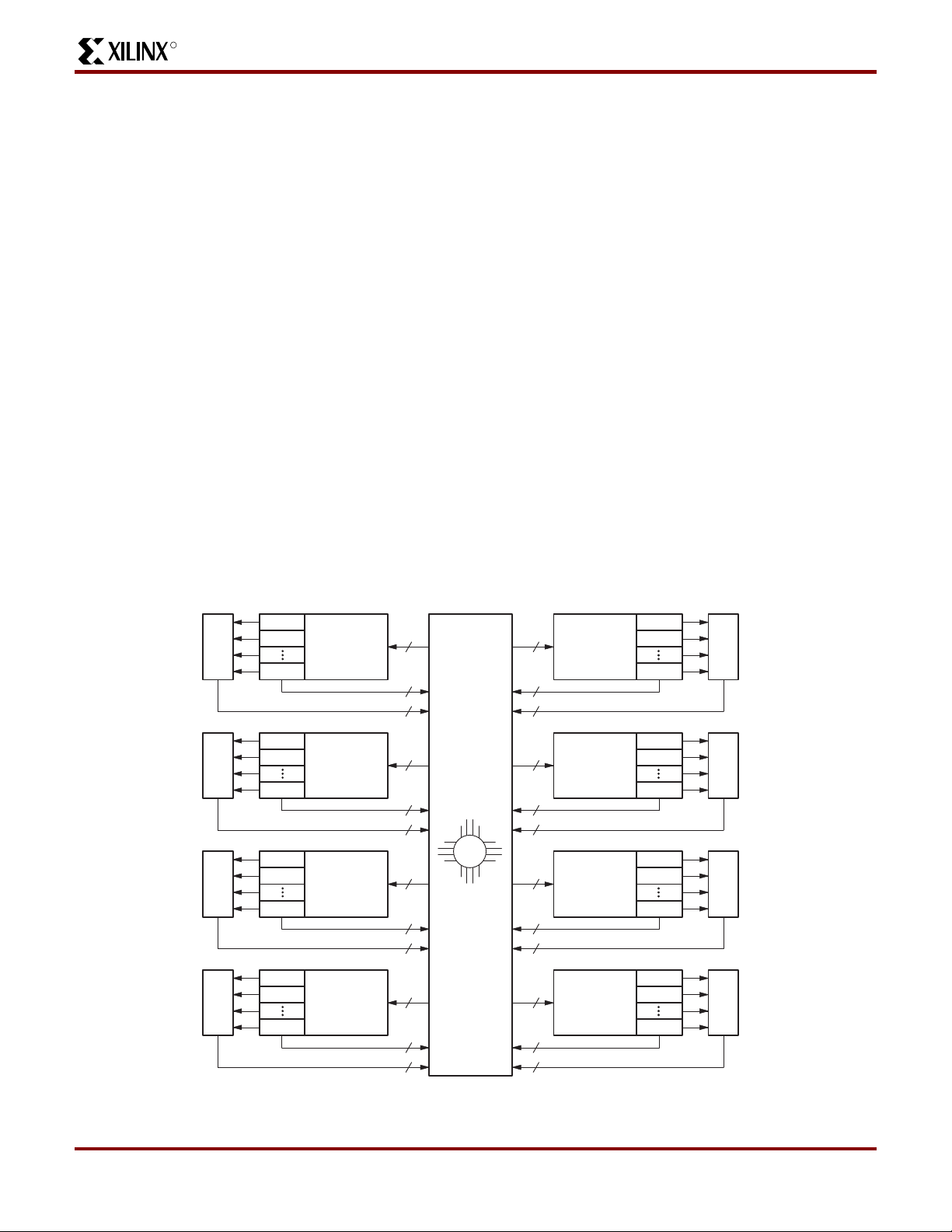
Figure 1 shows a high-level block diagram of a 128 macro-
cell device implementing the XPLA architecture. The XPLA
architecture consists of logic b loc ks that are interconnected
by a zero-power Interconnect Array (ZIA). The ZIA is a virtual crosspoint switch. Each logic block is essentially a
36V16 device with 36 inputs from the ZIA and 16 macrocells. Each logic bloc k also pro vides 32 ZIA f eedbac k paths
from the macrocells and I/O pins.
From this point of view, this architecture looks like many
other CPLD architectures. What makes the CoolRunner
family unique is what is inside each logic block and the
design technique used to implement these logic blocks.
The contents of the logic block will be described next.
Logic Block Architecture
Figure 2 illustrates the logic block architecture. Each logic
block contains control terms, a PAL array, a PLA array, and
16 macrocells. The six control terms can individually be
configured as either SUM or PRODUCT terms, and are
used to control the preset/reset and output enables of the
16 macrocells’ flip-flops. In addition, two of the control
terms can be used as clock signals (see Macrocell Architecture section for details). The PAL array consists of a programmable AND array with a fixed OR array, while the PLA
array consists of a programmable AND array with a programmable OR array. The PAL arra y pr ovides a high speed
path through the array, while the PLA array provides
increased product term density.
Each macrocell has five dedicated product terms from the
PAL array. The pin-to-pin t
through the PAL array is 7.5 ns. If a macrocell needs more
than five product terms, it simply gets the additional product
terms from the PLA array. The PLA array consists of 32
product terms, which are available for use by all 16 macrocells. The additional propagation delay incurred by a macrocell using one or all 32 PLA product terms is just 1.5 ns.
So the total pin-to-pin t
PD
product terms is 9 ns (7.5 ns for the PAL + 1.5 ns for the
PLA).
of the XCR3128A device
PD
for the XCR3128A using six to 37
I/O
I/O
I/O
I/O
MC0
MC1
MC15
MC0
MC1
MC15
MC0
MC1
MC15
MC0
MC1
MC15
LOGIC
BLOCK
LOGIC
BLOCK
LOGIC
BLOCK
LOGIC
BLOCK
MC0
36
16
16
36
16
16
ZIA
36
16
16
36
16
16
36
16
16
36
16
16
36
16
16
36
16
16
LOGIC
BLOCK
LOGIC
BLOCK
LOGIC
BLOCK
LOGIC
BLOCK
MC1
MC15
MC0
MC1
MC15
MC0
MC1
MC15
MC0
MC1
MC15
I/O
I/O
I/O
I/O
SP00464
Figure 1: Xilinx XPLA CPLD Architecture
DS035 (v1.2) August 10, 2000 www.xilinx.com 2
1-800-255-7778
Page 3
XCR3128A: 128 Macrocell CPLD with Enhanced Clocking
36 ZIA INPUTS
R
CONTROL
PAL
ARRAY
6
5
TO 16 MACROCELLS
PLA
ARRAY
(32)
SP00435A
Figure 2: Xilinx XPLA Logic Block Architecture
3 www.xilinx.com DS035 (v1.2) August 10, 2000
1-800-255-7778
Page 4
R
XCR3128A: 128 Macrocell CPLD with Enhanced Clocking
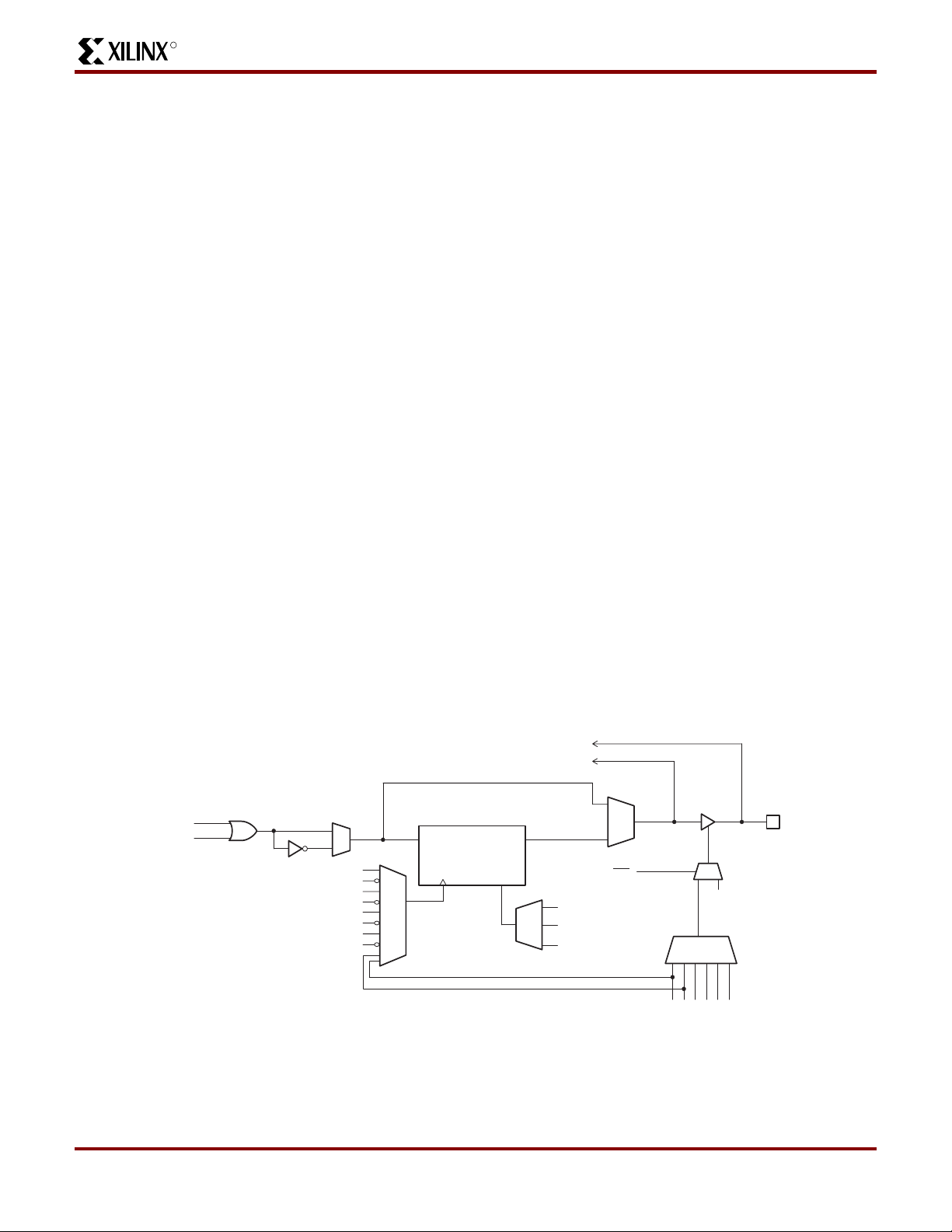
Macrocell Architecture
Figure 3 shows the architecture of the macrocell used in
the CoolRunner XCR3128A. The ma crocell can be configured as either a D- or T-type flip-flop or a combinatorial logic
function. A D-type flip-flop is generally more useful for
implementing state machines and data buffering while a
T-type flip-flop is generally more useful in implementing
counters. Each of these flip-flops can be clocked from any
one of six sources. Four of the cloc k s ourc es (CLK0, CLK1,
CLK2, CLK3) are connected to low-skew , devic e-wide clock
networks designed to preserve the integrity of the clock signal by reducing skew between rising and falling edges.
Clock 0 (CLK0) i s designated as a "synchronous" c loc k and
must be driven by an external source. Clock 1 (CLK1),
Clock 2 (CLK2), and Clock 3 (CLK3) can be used as "synchronous" clocks that are driven by an external source, or
as "asynchronous" clocks that are driven by a macrocell
equation. CLK0, CLK1, CLK2, and CLK3 can clock the
macrocell flip-flops on either the rising edge or the falling
edge of the clock signal. The other cl oc k sources are tw o of
the six control terms (CT2 and CT3) pr ovided in each logic
block. These cloc ks c an be indiv idually configured as either
a PRODUCT term or S UM term equation created from the
36 signals available inside the logic block. The timing for
asynchronous and control term clocks is different in that the
time is extended by the amount of time that it takes for
t
CO
the signal to propagate through the array and reach the
clock network, and the t
The six control terms of each logi c b loc k ar e used to control
the asynchronous Preset/Reset of the flip-flops and the
enable/disable of the output buff ers in each macr ocell. Control terms CT0 and CT1 are used to control the asynchro-
time is reduced.
SU
nous Preset/Reset of the macrocell’s flip-flop. Note that the
Power-on Reset leaves all macrocells in the "zero" state
when power is properly applied, and that the Preset/Reset
feature for each macrocell can also be disabled. Control
terms CT2 and CT3 can be used as a clock signal to the
flip-flops of the macrocells, and as the Output Enable of the
macrocell’s output buffer. Control terms CT4 and CT5 can
be used to control the Output Enab le of the macrocell’s out-
put buffer. Having four dedicated Output Enable control
terms ensures that the C oolRunner devices are PCI compliant. The output buffers can also be always enabled or
always disabled. All CoolRunner devices also provide a
Global 3-state (GTS) pin, which, when ena bled and pulled
Low, will 3-state all the outputs of the device. This pin is
provided to support "In-Circuit Testing" or "Bed-of-Nails"
testing.
There are two feedback paths to the ZIA: one from the macrocell, and one from the I/O pin. The ZIA feedback path
before the output buffer is the macrocell feedback path,
while the ZIA feedback path after the output buffer is the I/O
pin feedback path. When the macrocell is used as an output, the output buffer is enabled, and the macrocell feedback path can be used to feedback the logic implemented
in the macrocell. When the I/O pin is used as an input, the
output buffer will be 3-stated and the input signal will be fed
into the ZIA via the I/O feedback path, and the logic implemented in the buried macrocell can be fed back to the ZIA
via the macrocell feedback path. It should be noted that
unused inputs or I/Os should be properly terminated (see
the section on T erminations in this data sheet and the application note Ter minating Unused I/O Pins in Xilinx XPLA1
and XPLA2 CoolRunner CPLDs.
TO ZIA
PAL
PLA
CLK0
CLK0
CLK1
CLK1
CLK2
CLK2
CLK3
CLK3
D/T Q
INIT
(P or R)
CT0
CT1
GND
GTS
CT2
CT3
GND
CT4
CT5VGND
CC
SP00558
Figure 3: XCR3128A Macrocell Architecture
DS035 (v1.2) August 10, 2000 www.xilinx.com 4
1-800-255-7778
Page 5
XCR3128A: 128 Macrocell CPLD with Enhanced Clocking
R
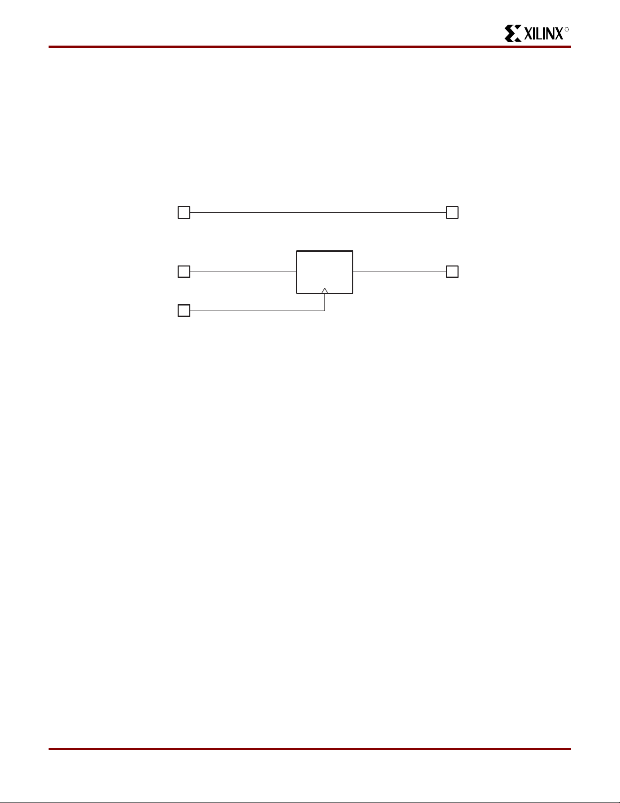
Simple Timing Model
Figure 4 shows the CoolRunner Timing Model. The C ool-
Runner timing model looks very much like a 22V10 timing
model in that there are three main timing parameters,
including t
tures, the user may be able to fit the design into the CPLD,
but is not sure whether system timing requirements can be
met until after the design has been fit into the device . This is
Figure 4: CoolRunner Timing Model
, tSU, and tCO. In other competing architec-
PD
t
PD_PAL
t
PD_PLA
REGISTERED
t
= PAL ONLY
SU_PAL
= PAL + PLA
t
SU_PLA
GLOBAL CLOCK PIN
= COMBINATORIAL PAL ONLY
= COMBINATORIAL PAL + PLA
because the timing models of competing architectures are
very complex and include such things as timing dependencies on the number of parallel expanders borrowed, sharable expanders, varying number of X and Y routing
channels used, etc. In the XPLA architecture, the user
knows up front whether the design will meet system timing
requirements. This is due to the simplicity of the timing
model.
OUTPUT PININPUT PIN
REGISTERED
t
CO
OUTPUT PININPUT PIN DQ
SP00553
5 www.xilinx.com DS035 (v1.2) August 10, 2000
1-800-255-7778
Page 6

R
XCR3128A: 128 Macrocell CPLD with Enhanced Clocking
TotalCMOS D es i gn Technique for Fast Zero
Power
Xilinx is the first to offer a TotalCMOS CPLD, both in process technology and design technique. Xilinx employs a
cascade of CMOS gates to implement its Sum of Products
instead of the traditional sense amp approach. This C MOS
70
60
50
40
I
CC
(mA)
30
gate implementation allows Xilinx to offer CPLDs which are
both high-performance and low power, breaking the paradigm that to have low power, you must have low performance. Refer to Figure 5 and Table 1 showing the I
CC
vs.
Frequency of the XCR3128A TotalCMOS CPLD (data
taken with eight up/down, loadable 16-bit counters at 3.3V,
25°C).
20
10
0
Figure 5: I
Table 1: I
120406080100
vs. Frequency @ VCC = 3.3V, 25°C
CC
vs. Frequency (VCC = 3.3V, 25°C)
CC
FREQUENCY (MHz)
120
SP00617
Frequency (MHz) 0 1 20 40 60 80 100 120
Typical I
(mA) 0.03 0.7 12.7 25.5 38.1 50.5 62.8 74.7
CC
DS035 (v1.2) August 10, 2000 www.xilinx.com 6
1-800-255-7778
Page 7

XCR3128A: 128 Macrocell CPLD with Enhanced Clocking
R
JTAG Te st i n g Capability
JTAG is the commonly-used acronym for the
Boundary-scan Test (BST) feature defined for integrated
circuits by IEEE Standard 1149.1. This standard defines
input/output pins, logic control functions, and commands
which facilitate both board and device level testing without
the use of specialized test equipment. The Xilinx
XCR3128A devices use the JTAG Interface for In-System
Programming/Reprogramming. Although only a subset of
the full JTAG command set is implemented (see Table 2),
the devices are fully capab le of sitting in a JTAG scan chain.
The Xilinx XCR3128A’s JTAG interface incl udes a TAP Port
defined by the IEEE 1149.1 JTAG Specification. As implemented in the Xilinx XCR3128A, the T AP P ort includes four
of the five pins (refer to Table 3) described in the JTAG
specification: TCK, TMS, TDI, and TDO. The fifth signal
defined by the JTAG specification is TRST* (Test Reset).
TRST* is considered an optional signal, since it is not actually required to perform BST or ISP. The Xilinx XCR3128A
saves an I/O pin for general purpose use by not implementing the optional TRST* signal in the JTAG interface.
Instead, the Xilinx XCR3128A supports the test reset functionality through the use of its power-up reset circuit, which
is included in all Xilinx CPLDs. The pins associated with the
TAP Port should connect to an external pull-up resistor to
keep the JTAG signals from floating when they are not
being used. In the Xilinx XCR3128A, the four mandatory
JTAG pins each require a unique, dedicated pin on the
device. The devices come from the factory with these I/O
pins set to perform JTAG functions, but through the software, the final function of these pins can be controlled. If
the end application will require the device to be reprogrammed at some future time with ISP, then the pins can be
left as dedicated JTAG functions, which means they are not
available for use as general purpose I/O pins. However,
unlike competing CPLDs, the Xilinx XCR3128A allow the
macrocells associated with these pins to be used as buried
logic when the JTAG/ISP function is enabled. This is the
default state for the software, and no action is required to
leave these pins enabled for the JTAG/ISP functions. If,
however, JTAG/ISP is not required in the end application,
the software can specify that this function be turned off and
that these pins be used as general purpose I/O. Because
the devices initially have the JTAG/ISP functions enabled,
the JEDEC file can be downloaded into the device once,
after which the JTAG/ISP pins will become general purpose
I/O. This feature is good for manufacturing because the
devices can be programmed during test and assembly of
the end product and yet still use all of the I/O pins after the
programming is done. It eliminates the need for a costly,
separate programming step in the manufacturing process.
Of course, if the JTAG/ISP function is never required, this
feature can be turned off in the s oftw are and the de v ice c an
be programmed with an industry-standard programmer,
leaving the pins available for I/O functions. Table 4 defines
the dedicated pins used by the four mandatory JTAG signals for each of the XCR3128A package types.
Table 2: XCR3128A Low -level JTAG Boundar y-scan Commands
Instruction
(Instruction Code)
Register Used
Bypass
(1111)
Bypass Register
Places the 1-bit bypass register between the TDI and TDO pins, which allows the BST
data to pass synchronously through the selected device to adjacent devices during
normal device operation. The Bypass instruction can be entered by holding TDI at a
constant high value and completing an Instruction-scan cycle.
Idcode
(0001)
Boundary-scan Register
Selects the IDCODE register and places it between TDI and TDO, allowing the
IDCODE to be serially shifted out of TDO. The IDCODE instruction permits blind
interrogation of the components assembled onto a printed circuit board. Thus, in
circumstances where the component population may vary, it is possible to determine
what components exist in a product.
Description
7 www.xilinx.com DS035 (v1.2) August 10, 2000
1-800-255-7778
Page 8

R
XCR3128A: 128 Macrocell CPLD with Enhanced Clocking
Table 3: JTAG Pin Description
Pin Name Description
TCK Test Clock Output Clock pin to shift the ser ial data and instructions in and out of the TDI and TDO pi ns,
respectively.
TMS Test M ode Select Serial input pin selects the JTAG instruction mode. TMS should be driven High
during user mode operation.
TDI Test Data Input Serial input pin for instructions and test data. Data is shifted in on the rising edge of
TCK.
TDO Test Data Output Serial output pin for instructions and test data. Data is shifted out on the falling edge
of TCK. The signal is 3-stated if data is not being shifted out of the device.
Table 4: XCR3128A JTAG Pinout by Package Type
Device
XCR3128A
TCK TMS TDI TDO
(Pin Number / Macrocell #)
100-pin VQFP 62/F15 15/C15 4/B15 73/G15
128-pin TQFP 82/F15 21/C15 8/B15 95/G15
3.3V, In-Syst em Programmin g (IS P )
ISP is the ability to reconfigure the logic and functionality of
a device, printed circuit board, or complete electronic system before, during, and after its manufacture and shipment
to the end customer. ISP provides substantial benefits in
each of the following areas:
• Design
- Faster time-to-market
- Debug partitioning and simplified prototyping
- Printed circuit board reconfiguration during debug
- Better device and board level testing
• Manufacturing
- Multi-functional hardware
- Reconfigurability for test
- Eliminates handling of "fine lead-pitch" components
for programming
- Reduced inventory and manufacturing costs
- Improved quality and reliability
• Field Support
- Easy remote upgrades and repair
- Support for field configuration, reconfiguration, and
customization
The Xilinx XCR3128A allows for 3.3V in-system programming/reprogramming of its EEPROM cells via its JTAG
interface. An on-chip charge pump eliminates the need for
externally provided supervoltages, so that the XCR3128A
may be easily programmed on the circuit board using only
the 3V supply required by the device for normal operation.
A set of low-level ISP basic commands implemented in the
XCR3128A enable this feature. The ISP commands implemented in the Xilinx XCR3128A are specified in Table 5.
Please note that an ENABLE command must precede all
ISP commands unless an ENABLE command has already
been given for a preceding ISP command.
DS035 (v1.2) August 10, 2000 www.xilinx.com 8
1-800-255-7778
Page 9

XCR3128A: 128 Macrocell CPLD with Enhanced Clocking
Table 5: Low Level ISP Commands
R
Instruction
(Register Used)
Enable
Instruction Code Description
1001 Enables the Erase, Program, and Verify commands.
(ISP Shift Register)
Erase
1010 Erases the entire EEPROM array.
(ISP Shift Register)
Program
1011 Programs the data in the ISP Shift Register into the addressed
(ISP Shift Register)
Verify
1100 Transfers the data from the addressed row to the ISP Shift
(ISP Shift Register)
Terminations
The CoolRunner XCR3128A CPLDs are TotalCMOS
devices. As with other CMOS devices, it is important to
consider how to properly terminate unused inputs and I/O
pins when fabricating a PC board. Allowing unused inputs
and I/O pins to float can cause the voltage to be in the li near
region of the CMOS input str uctures, which can increase
the power consumption of the device. The XCR3128A
CPLDs have programmable on-chip pull-down resistors on
each I/O pin. These pull-downs are automatically activated
by the fitter software f or all unused I/O pins. Note that an I/O
macrocell used as buried logic that does not have the I/O
pin used for input is considered to be unused, and the
pull-down resistors will be turned on. We recommend that
any unused I/O pins on the XCR3128A device be left
unconnected.
EEPROM row.
Register. .
There are no on-chip pull-down structures associated with
the dedicated input pins. Xilinx recommends that any
unused dedicated inputs be terminated with external 10kΩ
pull-up resistors. These pins can be directly connected to
or GND, but using the external pull-up resistors main-
V
CC
tains maximum design flexibility should one of the unused
dedicated inputs be needed due to future design changes.
When using the JTAG/ISP functions, it is also recommended that 10kΩ pull-up resistors be used on each of the
pins associated with the four mandatory JTAG signals. Letting these signals float can cause the voltage on TMS to
come close to ground, which could cause the device to
enter JTAG/ISP mode at unspecified times. See the application notes JTAG and ISP Overview for Xilinx XPLA1 and
XPLA2 CPLDs and Terminating Unused I/O Pi ns in Xilinx
XPLA1 and XPLA2 CoolRunner CPLDs for more informa-
tion.
9 www.xilinx.com DS035 (v1.2) August 10, 2000
1-800-255-7778
Page 10

R
XCR3128A: 128 Macrocell CPLD with Enhanced Clocking
JTAG and ISP Interfacing
A number of industry-established methods exist for
JTAG/ISP interfacing with CPLD’s and other integrated circuits. The Xilinx XCR3128A supports the following methods:
• PC parallel port
• Workstation or PC serial port
• Embedded Processor
• Automated test equipment
• Third party programmers
• High-end ISP tools
For more details on JTAG and ISP for the XCR3128A, refer
to the related application note: JTAG and ISP Overview for
Xilinx XPLA1 and XPLA2 CPLDs
Table 6: Programming Specifications
Symbol Parameter Min. Max. Unit
DC Parameters
V
CCP
I
CCP
V
IH
V
IL
V
SOL
V
SOH
TDO_I
TDO_I
OL
OH
VCC supply program/verify 3.0 3.6 V
ICC limit program/verify 200 mA
Input voltage (High) 2.0 V
Input voltage (Low) 0.8 V
Output voltage (Low) 0.5 V
Output voltage (High) 2.4 V
Output current (Low) 8 mA
Output current (High) -8 mA
AC Parameters
f
MAX
CLK maximum frequency 10 MHz
PWE Pulse width erase 100 ms
PWP Pulse width program 10 ms
PWV Pulse width verify 10 µs
INIT Initialization time 100 µs
TMS_SU TMS setup time before TCK goes High 10 ns
TDI_SU TDI setup time before TCK goes High 10 ns
TMS_H TMS hold time after TCK goes High 25 ns
TDI_H TDI hold time after TCK goes High 25 ns
TDO_CO TDO valid after TCK goes Low
40 ns
DS035 (v1.2) August 10, 2000 www.xilinx.com 10
1-800-255-7778
Page 11

XCR3128A: 128 Macrocell CPLD with Enhanced Clocking
R
Absolute Maximum Ratings
1
Symbol Parameter Min. Max. Unit
V
CC
V
I Input voltage -1.2 5.75 V
V
OUT
I
IN Input current -30 30 mA
T
J
T
str
Notes:
1. Stresses above those listed may cause malf unction or perma nent dam age to the device. This is a stress rating only.
2. The chip supply voltage must rise monotonically.
Supply voltage
Output voltage -0.5 5.5 V
Maximum junction temperature -40 150
Storage temperature -65 150
Functional operation at these or any other condition above those indicated in the operational and programming specification
is not implied.
2
-0.5 4.6 V
Operating Range
Product Grade Temperature Voltage
Commercial 0 to +70
Industrial -40 to +85
°
C 3.0 to 3.6 V
°
C 2.7 to 3.6 V
°C
°C
DC Electrical Characteristics For Commercial Grade Devices
Commercial: 0°C ≤ T
Symbol Parameter Test Conditions Min. Max. Unit
V
IL
V
IH
V
I
V
OL
V
OH
I
I
I
OZ
I
CCQ
I
CCD
I
OS
C
IN
C
CLK
C
I/O
Notes:
1
1, 2
Input voltage Low VCC = 3.0V 0.8 V
Input voltage High VCC = 3.6V 2.0 V
Input clamp voltage VCC = 3.0V, IIN = -18 mA -1.2 V
Output voltage Low VCC = 3.0V, IOL = 12 mA 0.5 V
Output voltage High VCC = 3.0V, IOH = -12 mA 2.4 V
Input leakage current VIN = 0 to 5.5V -10 10 µA
3-stated output leakage current VIN = 0 to 5.5V -10 10 µA
Standby current VCC = 3.6V, T
Dynamic current VCC = 3.6V, T
Short circuit output current
Input pin capacitance
Clock input capacitance
I/O pin capacitance
1. See Table 2 on page 7 typical values.
2. This parameter measured with a 16-bit, loadable up/down counter loaded into every logic block, with all outputs disabled
and unloaded. Input s are tied to V
3. Typical valu e s , not tested.
≤ +70°C; 3.0V ≤ VCC ≤ 3.6V
AMB
3
3
3
3
or ground. This parameter guar ant eed by design and characterization, not testing.
CC
= 0°C 100 µA
AMB
= 0°C @ 1 MHz 2 mA
AMB
V
= 3.6V, T
C
One pin at a time for no longer than one
= 0°C @ 50 MHz 50 mA
AMB
-50 -200 mA
second
T
= 25°C, f = 1 MHz 8 pF
AMB
T
= 25°C, f = 1 MHz 5 12 pF
AMB
T
= 25°C, f = 1 MHz 10 pF
AMB
11 www.xilinx.com DS035 (v1.2) August 10, 2000
1-800-255-7778
Page 12

R
XCR3128A: 128 Macrocell CPLD with Enhanced Clocking
AC Electrical Characteristics1 For Commercial Grade Devices
Commercial: 0°C ≤ T
≤ +70°C; 3.0V ≤ VCC ≤ 3.6V
AMB
Symbol Parameter
t
PD_PAL
Propagation delay time, input (or
feedback node) to output through PAL
t
PD_PLA
Propagation delay time, input (or
feedback node) to output through PAL +
PLA
t
CO
Clock to out (global synchronous clock
from pin)
t
SU_PAL
Setup time (from input or feedback node)
through PAL
t
SU_PLA
Setup time (from input or feedback node)
through PAL + PLA
SUPAL
SUPAL
2
2
2
2
2
+ tCF)
+ tCO)
t
H
t
CH
t
CL
t
R
t
F
f
MAX1
f
MAX2
f
MAX3
t
BUF
t
PDF_PAL
Hold time
Clock Hi gh time
Clock Low time
Input rise time
Input fall time
Maximum FF toggle rate2 1/(tCH + tCL) 250 200 167 MHz
Maximum internal frequency
1/(t
Maximum external frequency
1/(t
Output buffer delay time
Input (or feedback node) to internal
feedback node delay time through PAL
t
PDF_PLA
t
CF
t
INIT
t
ER
t
EA
t
RP
t
RR
Notes:
Input (or feedback node) to internal
feedback node delay time through
PAL+PLA
2
Clock to internal feedback node delay
2
time
Delay from valid VCC to valid reset
Input to output disable
Input to output valid
Input to register preset
Input to register reset
1. Specifications me asured with one outpu t switching. See Figure 6 and Table 7 f or derating.
2. This parameter guarant eed by desi gn and characterization, not by test.
3. Output C
= 5 pF.
L
71012Unit
Min. Max. Min. Max. Min. Max.
2 7.5 2 10 2 12 ns
3 9 3 11.5 3 13.5 ns
25.52728ns
3.5 4 6 ns
55.57.5ns
000ns
22.53ns
22.53ns
100 100 100 ns
100 100 100 ns
2
2
2
143 118 91 MHz
111 91 71 MHz
222ns
25.527.52 8 ns
2
373939.5ns
3.5 4.5 5 ns
2
2, 3
2
2
2
20 20 20 µs
8 9.5 10 ns
8 9.5 10 ns
9 9.5 10 ns
9 9.5 10 ns
DS035 (v1.2) August 10, 2000 www.xilinx.com 12
1-800-255-7778
Page 13

XCR3128A: 128 Macrocell CPLD with Enhanced Clocking
DC Electrical Characteristics For Industrial Grade Devices
R
Industrial: -40°C ≤ T
≤ +85°C; 2.7V ≤ VCC ≤ 3.6V
AMB
Symbol Parameter Test Conditions Min. Max. Unit
V
IL
V
IH
V
I
V
OL
V
OH
I
I
I
OZ
I
CCQ
I
CCD
I
OS
C
IN
C
CLK
C
I/O
Notes:
1
1 2
Input voltage Low VCC = 2.7V 0.8 V
Input voltage High VCC = 3.6V 2.0 V
Input clamp voltage VCC = 2.7V, IIN = -18 mA -1.2 V
Output voltage Low VCC = 2.7V, IOL = 8 mA 0.5 V
= 3.0V, IOL = 12 mA 0.5 V
V
CC
Output voltage High VCC = 2.7V, IOH = -8 mA 2.4 V
= 3.0V, IOH = -12 mA 2.4 V
V
CC
Input leakage current VIN = 0 to 5.5V -10 10 µA
3-stated output leakage current VIN = 0 to 5.5V -10 10 µA
Standby current VCC = 3.6V, T
Dynamic current VCC = 3.6V, T
= 3.6V, T
V
CC
Short circuit output current
Input pin capacitance
Clock input capacitance
I/O pin capacitance
1. See Table 1 on page 6 for typical values.
2. This parameter measured with a 16-bit, loadable up/down counter loaded into every logic block, with all outputs disabled
and unloaded. Input s are tied to V
3. Typical valu e s , not tested.
3
3
1 pin at a time for no longer than 1 second -50 -230 mA
3
3
T
= 25°C, f = 1 MHz 8 pF
AMB
T
= 25°C, f = 1 MHz 5 12 pF
AMB
T
= 25°C, f = 1 MHz 10 pF
AMB
or ground. This parameter guar ant eed by design and characterization, not testing.
CC
= -40°C 100 µA
AMB
= -40°C @ 1 MHz 2 mA
AMB
= -40°C @ 50 MHz 50 mA
AMB
13 www.xilinx.com DS035 (v1.2) August 10, 2000
1-800-255-7778
Page 14

R
XCR3128A: 128 Macrocell CPLD with Enhanced Clocking
AC Electrical Characteristics1 For Industrial Grade Devices
Industrial: -40°C ≤ T
≤ +85°C; 2.7V ≤ VCC ≤ 3.6V
AMB
Symbol Parameter
t
PD_PAL
Propagation delay time, input (or feedback node) to output through PAL
t
PD_PLA
Propagation delay time, input (or feedback node) to output through PAL + PLA
t
CO
t
SU_PAL
t
SU_PLA
Clock to out (global synchronous clock from pin) 2728ns
Setup time (from input or feedback node) through PAL 4 6 ns
Setup time (from input or feedback node) through
PAL + PL A
t
H
t
CH
t
CL
t
R
t
F
f
MAX1
f
MAX2
f
MAX3
t
BUF
t
PDF_PAL
t
PDF_PLA
Hold time 0 0 ns
Clock High time 3 4 ns
Clock Low time 3 4 ns
Input rise time 100 100 ns
Input fall time 100 100 ns
Maximum FF toggle rate 2 1/(tCH + tCL) 167 125 MHz
Maximum internal frequency 2 1/(t
Maximum external frequency 2 1/(t
Output buffer delay time
Input (or feedback node) to internal feedback node delay
time through PAL
2
Input (or feedback node) to internal feedback node delay
time through PAL+PLA
t
t
t
t
t
t
Notes:
CF
INIT
ER
EA
RP
RR
1. Specifications me asured with one outpu t switching. See Figure 6 and Table 7 f or derating.
2. This parameter guarant eed by desi gn and characterization, not by test.
3. Output C
Clock to internal feedback node delay time
Delay from valid VCC to valid reset
Input to output disable
Input to output valid
2
Input to register preset
Input to register reset
= 5 pF.
L
2
2
2, 3
2
10 15
Unit
Min. Max. Min. Max.
210215ns
3 11.5 3 16.5 ns
5.5 7.5 ns
+ tCF) 111 87 MHz
SUPAL
+ tCO)91 77 MHz
SUPAL
2
22ns
2829ns
3 9.5 3 10.5 ns
2
2
55.5ns
20 20 µs
10 12 ns
10 12 ns
10 12 ns
10 12 ns
DS035 (v1.2) August 10, 2000 www.xilinx.com 14
1-800-255-7778
Page 15

XCR3128A: 128 Macrocell CPLD with Enhanced Clocking
NUMBER OF OUTPUTS SWITCHING
1 2 4 8 12 16
5.1
t
PD_PAL
(ns)
5.3
5.4
5.6
VDD = 3.3V, 25°C
SP00698
5.7
5.8
5.2
5.5
5.9
6.0
6.1
Switching Characteristics
The test load circuit and load values for the AC Electrical Characteristics are illustrated below.
V
DD
R
S1
Component Values
R1 390Ω
R2 390Ω
R1
V
IN
V
OUT
C1 35 pF
Measurement S1 S2
R2
S2
C1
t
PZH
t
PZL
t
P
NOTE: For t
measured
Open Closed
Closed Open
Closed Closed
PHZ
and t
C = 5 pF, and 3-state levels are
PLZ
0.5V from steady state active level.
+3.0V
SP00699
90%
10%
1.5ns1.5ns
SP00368
0V
t
t
R
F
MEASUREMENTS:
All circuit delays are measured at the +1.5V level of
inputs and outputs, unless otherwise specified.
Input Pulses
Figure 7: Voltage Waveform
Figure 6: t
vs. Outputs Switching
PD_PAL
Table 7: t
(V
= 3.3 V, T = 25°C)
CC
Number of
Outputs
vs. Number of Outputs Switching
PD_PAL
1 2 4 8 12 16
Typical (ns) 5.3 5.3 5.4 5.6 5.9 6.1
15 www.xilinx.com DS035 (v1.2) August 10, 2000
1-800-255-7778
Page 16

R
XCR3128A: 128 Macrocell CPLD with Enhanced Clocking
Pin Function and Laynout
XCR3128A: 1 00 -pin VQFP, and 128-pin TQFP Pi n Function Table
Pin
#
1 I/O-A2 I/O-A3 33 I/O-D5 NC 65 I/O-G4 I/O-E15 97 I/O-A8 NC
2 I/O-A0 I/O-A2 34 V
3V
4 I/ O-B15 (TDI) NC 36 I/O-D2 I/O-C0 68 I/O-G7 NC 100 I/O-A4 I/O-H0
5 I/O-B13 NC 37 I/O-D0/CLK2 GND 69 I/O-G8 NC 101 - I/O-H2
6 I/O-B12 NC 38 GND I/O-D15 70 I/O-G10 NC 102 - I/O-H3
7I/O-B10 V
8 I/O-B8 I/O-B15 (T DI) 40 I/O-E0/
9 I/O-B7 I/O-B13 41 I/O-E2 I/O-D11 7 3 I/O-G15
10 I/O-B5 I/O-B12 42 I/O-E4 I/O-D10 74 GND I/O-F5 106 - I/O-H8
11 GND I/O-B11 43 GND I/O-D8 75 I/O-H0 I/O-F7 107 - I/O-H10
12 I/O-B4 I/O-B10 44 I/O-E5 I/O-D7 76 I/O-H2 I/O-F8 108 - V
13 I/O-B2 I/O-B8 45 I/O-E7 I/O-D5 77 I/O-H4 I/O-F10 109 - I/O-H11
14 I/O-B0 I/O-B7 46 I/O-E8 V
15 I/O-C15
16 I/O-C13 GND 48 I/O-E12 I/O-D3 80 I/O-H8 I/O-F12 112 - I/O-H15
17 I/O-C12 I/O-B4 49 I/O-E13 I/O-D2 81 I/O-H10 I/O-F13 113 - GND
18 V
19 I/O-C10 I/O-B2 51 V
20 I/O-C8 I/O-B0 52 I/O-F0 V
21 I/O-C7 I/O-C15
22 I/O-C5 I/O-C13 54 I/O-F4 I/O-E2 86 GND I/O-G4 118 - V
23 I/O-C4 I/O-C12 55 I/O-F5 I/O-E3 87 IN0/CLK0 V
24 I/O-C2 I/O-C11 56 I/O-F7 I/O-E4 88 IN2/gtsn I/O-G5 120 - I/O-A13
25 I/O-C0 V
26 GND I/O-C10 58 I/O-F10 I/O-E5 90 IN3 I/O-G8 122 - I/O-A12
27 I/O-D15 I/O-C8 59 GND I/O-E7 91 V
28 I/O-D13 I/O-C7 60 I/O-F12 I/O-E8 92 I/O-A15/CLK3 I/O-G11 124 - I/O-A10
29 I/O-D12 I/O-C5 61 I/O-F13 I/O-E10 93 I/O-A13 I/O-G12 1 25 - I/O-A8
30 I/O-D10 I/O-C4 62 I/O-F15
31 I/O-D8 I/O-C3 63 I/O-G0 I/O-E12 95 GND I/O-G15
32 I/O-D7 I/O-C2 64 I/O-G2 I/O-E13 96 I/O-A10 GND 1 28 - I/O-A4
Function
100-pin
VQFP
CC
(TMS)
CC
128-pin
TQFP
I/O-A0 35 I/O-D4 NC 67 I/O-G5 I/O-F0 99 I/O-A5 NC
CC
I/O-B5 47 I/O-E10 I/O-D4 7 9 I/O-H7 I/O-F11 1 11 - I/O-H13
I/O-B3 50 I/O-E15 I/O-D0/CLK2 82 V
(TMS)
CC
Pin
#
39 V
53 I/O-F2 I/O-E0/
57 I/O-F8 GND 89 IN1 I/O-G7 121 - I/O-A12
Function
100-pin
VQFP
CC
CC
CLK1
CC
(TCK)
128-pin
TQFP
NC 66 V
I/O-D13 71 I/O-G12 I/O-F2 103 - I/O-H4
I/O-D12 72 I/O-G13 I/O-F3 104 - I/O-H5
CC
GND 8 3 I/O-H12 I/O-G0 115 - IN2/gtsn
CC
CLK1
I/O-E11 94 I/O-A12 I/O-G13 126 - I/O-A7
Pin
#
78 I/O-H5 GND 110 - I/O-H12
84 I/O-H13 I/O-G2 116 - IN1
85 I/O-H15 I/O-G3 117 - IN3
Function
100-pin
VQFP
CC
(TDO)
CC
CC
128-pin
TQFP
V
CC
I/O-F4 1 05 - I/O-H7
I/O-F15
(TCK)
CC
I/O-G10 123 - GND
(TDO)
Pin
#
98 I/O-A7 NC
114 - IN0/CLK0
119 - I/O-A15/
127 - I/O-A5
Function
100-pin
VQFP
128-pin
TQFP
CC
CC
CLK3
DS035 (v1.2) August 10, 2000 www.xilinx.com 16
1-800-255-7778
Page 17

XCR3128A: 128 Macrocell CPLD with Enhanced Clocking
100-pin VQFP 128-pin TQFP
R
100 76
1
VQFP
TQFP
25
26 50
Ordering Information
Exam ple: XCR3128A -7 VQ 100 C
Device Type
Speed Options
75
51
SP00485A
128
1
TQFP
LQFP
38
39
Temperature Range
Number of Pins
Package Type
103
102
65
64
SP00469B
Speed Options
Temperature Range
-15: 15 ns pin-to-pin delay
-12: 12 ns pin-to-pin delay
-10: 10 ns pin-to-pin delay
-7: 7.5 ns pin-to-pin delay
Packaging Options
Component Avai lability
Pins 100 128
Type Plastic VQFP Plastic TQFP
Code VQ100 TQ128
XCR3128A -15 I I
-12 C C
-10 C, I C, I
-7 C C
Revision History
Date Version # Revision
7/22/99 1.0 Initial Xilinx release
2/10/00 1.1 Converted to Xilinx format and updated.
8/10/00 1.2 Updated pinout table.
C = Commercial, T
I = Industrial, T
= 0°C to +70°C
A
= –40°C to +85°C
A
VQ100: 100-pin VQFP
TQ128: 128-pin TQFP
17 www.xilinx.com DS035 (v1.2) August 10, 2000
1-800-255-7778
 Loading...