Page 1
SERVICE MANUAL
PA
011507
HAMAMATSU, JAPAN
0.27K-8091 Printed in Japan '00.03
CONTENTS
SPECIFICATIONS···································································· 3
PANEL LAYOUT······································································· 3
CONNECTOR CIRCUIT DIAGRAM ········································· 4
DISASSEMBLY PROCEDURE················································· 5
CIRCUIT BOARD······································································ 6
PARTS LIST
CIRCUIT DIAGRAM
POWER SUPPLY
Page 2
PW1D
2
WARNING: CHEMICAL CONTENT NOTICE!
The solder used in the production of this product contains LEAD. In addition, other electrical/electronic and/or plastic (where
applicable) components may also contain traces of chemicals found by the California Health and Welfare Agency (and possibly
other entities) to cause cancer and/or birth defects or other reproductive harm.
DO NOT PLACE SOLDER, ELECTRICAL/ELECTRONIC OR PLASTIC COMPONENTS IN YOUR MOUTH FOR ANY REASON
WHAT SO EVER!
Avoid prolonged, unprotected contact between solder and your skin! When soldering, do not inhale solder fumes or expose eyes
to solder/flux vapor!
If you come in contact with solder or components located inside the enclosure of this product, wash your hands before handling
food.
IMPORTANT NOTICE
This manual has been provided for the use of authorized Yamaha Retailers and their service personnel. It has been assumed that
basic service procedures inherent to the industry, and more specifically Yamaha Products, are already known and understood by
the users, and have therefore not been restated.
WARNING: Failure to follow appropriate service and safety procedures when servicing this product may result in personal
injury, destruction of expensive components and failure of the product to perform as specified. For these
reasons, we advise all Yamaha product owners that all service required should be performed by an authorized
Yamaha Retailer or the appointed service representative.
IMPORTANT: This presentation or sale of this manual to any individual or firm does not constitute authorization, certification,
recognition of any applicable technical capabilities, or establish a principal-agent relationship of any form.
The data provided is belived to be accurate and applicable to the unit(s) indicated on the cover. The research engineering, and
service departments of Yamaha are continually striving to improve Yamaha products. Modifications are, therefore, inevitable and
changes in specification are subject to change without notice or obligation to retrofit. Should any discrepancy appear to exist,
please contact the distributor's Service Division.
WARNING: Static discharges can destroy expensive components. Discharge any static electricity your body may have
accumulated by grounding yourself to the ground bus in the unit (heavy gauge black wires connect to this bus).
IMPORTANT: Turn the unit OFF during disassembly and parts replacement. Recheck all work before you apply power to the
unit.
WARNING
Components having special characteristics are marked and must be replaced with parts having specification equal to those
originally installed.
IMPORTANT NOTICE FOR THE UNITED KINGDOM
Connecting the Plug and Cord
IMPORTANT. The wires in this main lead are coloured in
accordance with the following code:
BLUE: NEUTRAL
BROWN: LIVE
As the colours of the wires in the main lead of this apparatus may not
correspond with the coloured markings identifying the terminals in
your plug, proceed as follows:
The BLUE wire must be connected to the terminal that is marked with
the letter N (or coloured BLACK).
The BROWN wire must be connected to the terminal that is marked
with the letter L (or coloured RED).
Be certain that neither core is connected to the earth terminal of the
three pin plug.
Page 3

SPECIFICATIONS
PW1D
3
Note: See operation manual for details.
PANEL LAYOUT
Page 4
PW1D
4
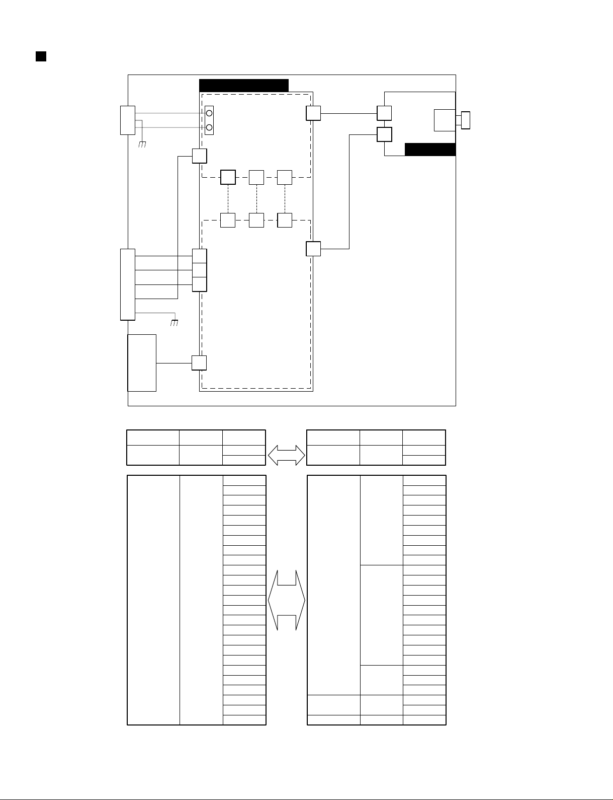
CONNECTOR CIRCUIT DIAGRAM
FAN
3P
CN1
3P
CN3
2P
CN8
(FOR LED)
2P
CN2
2P
CN101
9P
CN6
10P
CN7
3P
CN1
3P
(FOR FAN)
3P
CN2
3P
CN33PCN23PCN4
3P
CN42PCN5
27P
(MAIN)
[POWER]
[ON/OFF]
AC INLET
[DC OUTPUT]
3P
FG
CN1
FG
(SUB)
POWER
SUPPLY
PW1D
KEC-92552
PW-SW
CONSOLE-DC
**
**
Circuit Board CN No. Pin No.
AC INLET
N
L
POWER SUPPLY
PW1D (SUB)
1
2
CN1
Circuit Board CN No. Pin No.
DC OUTPUT 1
4
2
5
6
7
8
9
10
11
12
13
14
15
16
17
18
19
20
22
23
24
26
27
3
POWER
SUPPLY
PW1D
(MAIN)
POWER SUPPLY
PW1D (SUB)
CN6
CN7
CN1
CN101
1
2
3
4
5
6
7
8
9
1
2
3
4
5
6
7
8
9
10
1
2
3
1
2
FG
Page 5
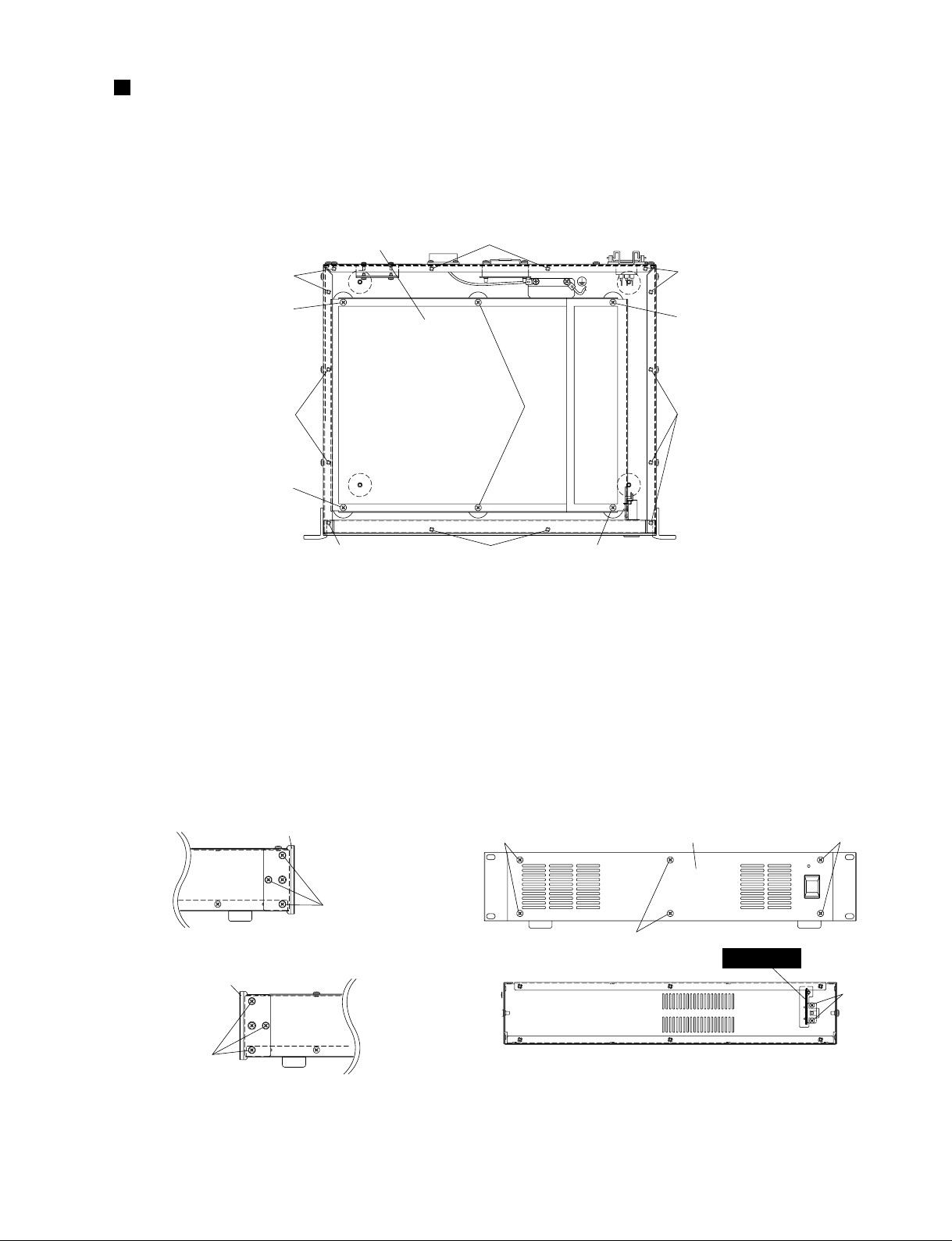
Fig. 2
[170]
[170]
[170]Front panel
Rack Mount Angle
Rack Mount Angle
[150]
[260]
[280]
[260]: Oval Head Screw-B 4.0x8 MFZN2BL (VS153600)
[280]: Oval Head Screw-B 4.0x8 MFZN2BL (VS153600)
[150]: Bind Head Screw 3.0x8 MFZN2BL (VB659000)
[170]: Oval Head Screw-B 4.0x8 MFZN2BL (VS153600)
• Left side <Front View>
• Right side
PW-SW
Power supply unit
[300]
[300] [130]
[130]
[300]
[130]
[300]
[130]
[130]
[300]
[300]
[300]
[130]: Bind Head Tapping Screw-B A4.0x8 MFZN2BL (VC688800)
[300]: Bind Head Tapping Screw-B A4.0x8 MFZN2BL (VC688800)
Fig. 1
DISASSEMBLY PROCEDURE
PW1D
5
1. Power Supply Unit
1-1 Remove the fourteen (14) screws marked [300]. The top
cover can then be removed. (Fig. 1)
1-2 Remove the six (6) screws marked [130]. The power
supply unit can then be removed. (Fig. 1)
2. PW-SW Circuit Board
2-1 Remove the three (3) screws marked [260] and the three
(3) screws marked [280]. Each rack mount angle can then
be removed. (Fig.2)
2-2 Remove the six (6) screws marked [170]. The front panel
can then be removed. (Fig. 2)
2-3 Remove the two (2) screws marked [260]. The PW-SW
circuit board can then be removed. (Fig. 2)
Page 6

3NA-V50504
Component side
POWER ON/OFF
Power supply PW1D
(SUB)
Power supply PW1D
(MAIN)
0
PW-SW Circuit Board
PW1D
6
CIRCUIT BOARD
Note: See parts list for details of circuit board component parts.
Page 7

CONTENTS
OVERALL ASSEMBLY······························································································································ 2
ELECTRICAL PARTS ······························································································································· 4
PARTS LIST
WARNING
Components having special characteristics are marked and must be replaced with parts having
specification equal to those originally installed.
A: Australian model
B: British model
C: Canadian model
D: German model
E: European model
F: French model
H: North European model
I : Indonesian model
J: Japanese model
M: South African model
O: Chinese model
Q: South-east Asia model
T: Taiwan model
U: U.S.A. model
V: General export model (110 V)
W: General export model (220 V)
N,X:General export model
Y: Export model
Notes : DESTINATION ABBREVIATIONS
• The numbers in “ QTY ” show quantities for each unit.
• The parts with “ - - ” in “ PART NO. ” are not available as spare parts.
• The mark “ ” in the remarks column indicates that these parts are interchangeable.
• The second letter of the shaded ( ) part number is O, not zero.
• The second letter of the shaded ( ) part number is I, not one.
POWER SUPPLY
Page 8

PW1D
2
OVERALL ASSEMBLY
10
40
50
20
30
60
70
35
130
120
120
310
320
230
160
170
100
290
300
300
300
330
140
110
150
180
190
250
260
270
280
90
98
97
95
96
80
91
240
210
200
350
360
370
220
Page 9

PW1D
3
OVERALL ASSEMBLY
Overall Assembly
Overall Assembly
Overall Assembly
Bottom Chassis
Leg
Bind Head Tapping Screw-B
PET Sheet
Side Panel
Bind Head Tapping Screw-B
Side Panel
Bind Head Tapping Screw-B
Rear Panel
Bind Head Tapping Screw-B
Bind Head Screw
Fan
Finger Guard
Fan Support Metal
Pan Head Screw
Sub Chassis
Bind Head Tapping Screw-B
Power Supply Unit
Power Supply Unit
Power Supply Unit
Bind Head Tapping Screw-B
Circuit Board
Bind Head Screw
Front Panel
Oval Head Screw
Escutcheon, Power Switch
Power Switch Knob
AC Inlet Assembly
AC Inlet
Support
Bind Head Screw
Connector Assembly
Bind Head Tapping Screw-B
Rack Mount Angle
Oval Head Screw
Rack Mount Angle
Oval Head Screw
Top Cover
Bind Head Tapping Screw-B
Connector Assembly
Connector Assembly
Label, Caution
Cord Binder
Label
Label
Label
Label
Cord Holder
ACCESSORIES
AC Cord
AC Cord
AC Cord
AC Cord
DC Power Supply Cable
Cable Lock
Cable Lock
DESCRIPTION
10
20
30
35
40
50
60
70
80
90
91
95
96
97
98
100
110
120
120
120
130
140
150
160
170
180
190
200
200a
210
220
230
240
250
260
270
280
290
300
310
320
330
340
350
350
360
370
380
REF NO.
- -
- -
- V4586900
CB806590
EG340190
V5297200
V4605100
VC688800
V4068400
VC688800
V4587400
VC688800
VP156800
V3125300
VN003900
VM964700
VR116500
V4587900
VC688800
V4704700
V5390500
V5390700
VC688800
V4564700
VB659000
V4587100
VS153600
VL813000
VL812900
- V5065200
V5600300
VP156800
V5054900
VP157000
V4705100
VS153600
V4705100
VS153600
V4588000
VC688800
- -
- -
- CB817510
- -
- -
- -
- CB095100
V5800000
V5068000
V5067700
VP204400
V5525000
V5600500
V5600800
PART NO.
BL
4.0X8 MFZN2BL
LEFT
A4.0X8 MFZN2BL
RIGHT
A4.0X8 MFZN2BL
A4.0X8 MFZN2BL
A4.0X8 MFZN2BL
MMS-06E12DL
SP 4.0X25 MFZN2BL
A4.0X8 MFZN2BL
A4.0X8 MFZN2BL
PW-SW (PSWCOM)
3.0X8 MFZN2BL
4.0X8 MFZN2BL
AC INLET&FASTON
M1908-C 3P
A4.0X8 MFZN2BL
VH&PH&NK 120L #20
A3.0X8 MFZN2BL
4.0X8 MFZN2BL
4.0X8 MFZN2BL
A4.0X8 MFZN2BL
VH&VH 3P 350L #20
PH&PH 2P 650L #28
S-14B
UL
2P 15A
3P 13A
3P 10A
3P
UL2501 #20X27
PW1D
J (V470350)
U,C,V (V539350)
H,B,W (V539360)
J
U,C,V
H,B,W
POWER ON/OFF
(V539260)
DC OUTPUT
(V505500)
(V477420)
(V533510)
J (V533540)
H,B,W (V539490)
U,C,V (V570430)
U,C,V (VA03930)
J
U,C,V
H,W
B
J,U,C,V
H,W,B
REMARKS
4
4
6
3
3
5
4
6
6
2
6
2
4
3
3
14
3
6
QTY
RANK
*
*
*
*
*
*
*
*
*
*
*
*
*
*
*
*
*
*
*
*
*
*
03
01
01
01
01
01
08
09
01
01
01
01
01
03
03
03
01
01
01
01
01
03
10
*
:
New Parts RANK: Japan only
Page 10

PW1D
4
ELECTRICAL PARTS
Circuit Board
Circuit Board
Spacer
Capacitor-KH
Base Post Connector
Connector Base Post
LED
Push Switch
Carbon Resistor
Fan
Power Supply Unit
Power Supply Unit
Power Supply Unit
AC Inlet
Connector Assembly
DESCRIPTION
C1
CN1
CN2
LD1
SW1
REF NO.
V4564700
V4564700
V4588100
V3311600
LB933030
VB389800
VR080300
V3127000
HF455680
V3125300
V4704700
V5390500
V5390700
V5065200
V5054900
PART NO.
PW-SW (PSWCOM)
PW-SW (PSWCOM)
0.010 250V J.U.C.S
VH 3P SE
PH 2P TE
SLR-342MG3F
ESB92S23B J.U.C.S
680.0 1/4 J
MMS-06E12DL
M1908-C 3P
VH&PH&NK 120L #20
PW1D
(XW730A0)
(XW730A0)
POWER indicator
POWER 0N/OFF
J
U,V
H,B,W
DC OUTPUT
REMARKS
QTY
RANK
*
*
*
*
*
*
*
*
01
01
01
01
02
01
08
03
ELECTRICAL PARTS
*
:
New Parts RANK: Japan only
Page 11

CIRCUIT DIAGRAM
WARNING
Components having special characteristics are marked and must be replaced with parts having
specification equal to those originally installed.
PO WER SUPPLY
PSWCOM ···························································3
CONSOLE-DC····················································4
CONTENTS
Page 12

GFH DC
BA
1
2
3
4
5
6
E
PSWCOM CIRCUIT DIAGRAM (PW1D
)
PW1D
PSWCOM CIRCUIT DIAGRAM (PW1D
)
KEC-92466-1
PW-SW
to CONSOLE-DC-CN3
to CONSOLE-DC-CN8
3
Page 13

BCDE
F
G
HIJ
K
LMN
O
P
A
12
10
11
5
6
7
8
9
4
3
1
2
CONSOLE-DC CIRCUIT DIAGRAM 1/3 (PW1D
)
PW1D
CONSOLE-DC CIRCUIT DIAGRAM 1/3 (PW1D
)
ZC-0159-A-1
1
2
3
CN1
B3B-PH-K-S
RY2A
G5N-1A
RY1A
G4W-1112P-US-TV8
RY1B
G4W-1112P-US-TV8
D1
ERA15-06V5
C1
100/25C20.1/50
Z1
430V
Z2
1500V
C5
0.1/250
C6
0.47/250
C7
0.47/250
R1
1M
D2
ERA15-06V5
CN8
B2B-PH-K-S
CN2
B2B-XH-A
1
2
3
CN3
B03P-VL
1
2
1
2
CN4
B2P-VH
from SUB POWER BOARD
from SUB POWER BOARD
from SUB POWER BOARD
to DC CONTROL BOARD
DC/DC
to PW-SW-CN2
to PW-SW-CN1
+12V
+18V
1
2
CN5
B2B-XH-A
TEST
1
2
L1
1mH/15A
L2
C8
2200P/250
TM1
110
o
C
R2
30P30
D4
D20XB60
R7
5P0.05
L3
L4
A
B
5mH/5A
AB1
AB2
15A/300uH
Q1
2SK1941
D6
PA905C6
Q2
2SK1941
C9
2200P/250
IC2
BA17812T
RY3B
G4W-1112P-US-TV8
RY3A
G4W-1112P-US-TV8
C10
0.01/250
C100
1.8/400
R8
1P3.3
D5
1GWJ43
R9
47K
R10
47K
R3
4.3
R4
150K(F)
R5
150K(F)
R6
150K(F)
R11
1P3.3
R12
120K(F)
R13
120K(F)
R14
120K(F)
C13
390/450
C14
390/450
D7
1GWJ43
C12
1.8/400
C11
0.01/250
D9
ERA15-06V5
R15
1P20K
D10
ERA15-06V5
D11
ERA15-06V5
R16
1P20K
R17
1P20K
R18
1P20K
R21
10K
C101
0.1/50
R25
1.2K
R32
1K
R33
1K(F)
R34
1K(F)
VR1
22KB
VR2
1KB
240u/6V
R24
2.4K
R27
10K(F)
R23
3.3K
R22
10K
R20
330
Q3
2SC2120
Q4
2SA933
R26
1P2.2
C24
10/50
C23
0.1/50
R31
33K
R29
470K
R30
33K
ZD1
MTZJ5.1B
C19
100/16
C25
68P/50
C26
0.1/50
C27
470P/50
C21
1.2/100
C22
470P/50
C28
0.15/50
C20
1/50
C16
47/35
D8
ERA15-06V5
C18
0.1/50
C17
0.1/50
RY2B
G5N-1A
1mH/15A
F1
15A/250V
IC3
FA5332P
10
12
14
16
7
5
3
1
9
11
13
15
8
6
4
2
4
Page 14

BCDE
F
G
HIJ
K
LMN
O
P
A
12
10
11
5
6
7
8
9
4
3
1
2
CONSOLE-DC CIRCUIT DIAGRAM 2/3 (PW1D
)
PW1D
CONSOLE-DC CIRCUIT DIAGRAM 2/3 (PW1D
)
ZC-0159-B-1
C29
390/450
C30
390/450
R35
47(F)
VR3
100B
R36
2P220K
R37
2P220K
R38
2P1.5
R39
2P1.5
C34
1000P/630
C40
1000P/630
R41
2P1.5
R40
2P1.5
R42
2P220K
R43
2P220K
R44
47(F)
VR4
100B
R45
2P2.2K
C39
1000P/630
C33
1000P/630
Q5
2SC4161-N
Q7
2SC4461-N
Q9
2SC4461-N
Q10
2SC4461-N
Q12
2SC4161-N
Q11
2SC4161-N
Q13
2SC1815-GR
Q8
2SC4461-N
Q6
2SC4161-N
IC4
C31
100/16
C32
100/16
C36
0.56/400
C35
0.56/400
C37
0.56/400
C41
100/16
C43
4700P/250
C44
4700P/250
C42
100/16
C38
0.56/400
T2
NT-322
A
B
BX6607
3
4
5
10
11
1
2
7
12
8
9
14
IC5
T1
NT-321
D12
1DL42A
D16
ERA15-06V5
D17
ERA15-06V5
D18
ERA16-06V5
ZD2
MTZJ5.1B
IC6
BA24T
C46
0.1/50
C45
47/50
C48
10/50
C49
680/100
C50
680/100
C51
680/100
C52
680/100
C53
680/100
C54
680/100
C15
0.1/100
C47
0.1/50
R46
1K
R47
10K
R49
1P22K
R50
1P2.2K
R51
1P4.3K
R52
2P22K
R53
2P22K
D13
1DL42A
D14
1DL42A
D15
1DL42A
R48
30P/30
D19
D20LC20U
D21
ERA15-06V5
RY5A
G4W-1112P-US-TV8
RY5B
G4W-1112P-US-TV8
RY4A
G4W-1112P-US-TV8
RY4B
G4W-1112P-US-TV8
TM2
110
o
C
D20
D20LC20U
BX6607
3
4
5
10
11
1
2
7
12
8
9
14
1
2
3
4
5
6
7
8
9
10
CN6
B10P-VH
1
2
3
4
5
6
7
8
9
CN7
B9P-VH
to D/D UNITS
5
Page 15
BCDE
F
G
HIJ
K
LMN
O
P
A
12
10
11
5
6
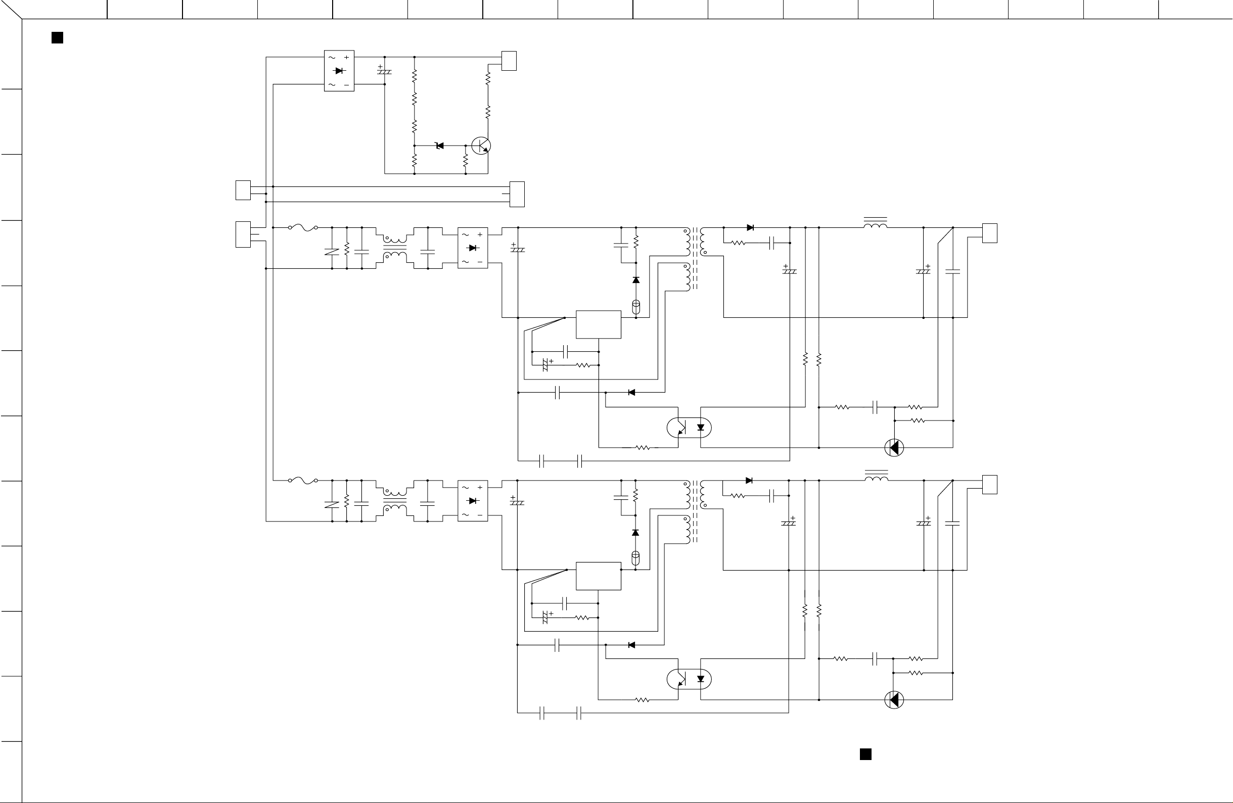
7
8
9
4
3
1
2
CONSOLE-DC CIRCUIT DIAGRAM 3/3 (PW1D
)
PW1D
CONSOLE-DC CIRCUIT DIAGRAM 3/3 (PW1D
)
ZC-0160-A-1
D101
D2SBA60
D5
D2SBA60
D1
D2SBA60
IC1
MIP0222SY
T1
NT-332A
D4
D3L20U
C5
0.1/50
R3
6.2
R5
1P33
C11
220/35
R6 330
R7
C27
0.1/50
C26
100/35
C13
0.1/50
C12
100/35
470
C10
390P/1K
T2
NT-333A
D8
D3L20U
R15
1P33
C25
220/35
R16 330
R17 470
C24
390P/1K
R4
6.2
C6
47/25
PC1
TLP721F
R8
10K
R9
39K(F)
R10
10K(F)
IC2
TA76431S
L4
10uH/1A
622LY-100K
L2
10uH/1A
622LY-100K
C14
0.1/50
R18
10K
R19
62K(F)
R20
10K(F)
IC4
TA76431S
C28
0.1/50
C7
0.1/50
C8
2200P/250C92200P/250
D3
1DL42A
23
C101
22/400
R101
1P22K
R102
1P22K
R103
1P27K
R104
5.1K(F)
Z1
430V
R1
1M
C1
0.1/250
Z2
430V
R11
1M
C15
0.1/250
C16
0.1/250
C17
33/400
D6
1JU41
C18
4700P/1K
R12
2P100K
C3
33/400
C2
0.1/250
C4
4700P/1K
R2
2P100K
D2
1JU41
R107
1.5K(F)
R106
2P22K
R105
2P22K
R13
6.2
IC101
2SC4815
ZD100
MTZJ5.1B
F1
1A/250
F2
1A/250
L1
18mH/0.5A
744003
L3
18mH/0.5A
744003
AB1
BEADS
1
IC3
MIP0222SY
C19
0.1/50
R4
6.2
C20
47/25
C21
0.1/50
C22
2200P/250
C23
2200P/250
D7
1DL42A
23
1
AB2
BEADS
PC2
TLP721F
1
2
3
CN3
B3P-VH
CN1
RT-02T-1.3B
1
2
1
2
3
CN2
B03P-VL
CN101
B2B-PH-K-S
1
2
CN4
B2P-VH
1
2
CN5
B2P-XH-A
1
2
INPUT
AC80~230V
to POWERSWITCH
to POWER CONVERTER BOARD
to POWER CONVERTER BOARD
+12V
OUTPUT
to POWER CONVERTER BOARD
+18V
OUTPUT
6
 Loading...