


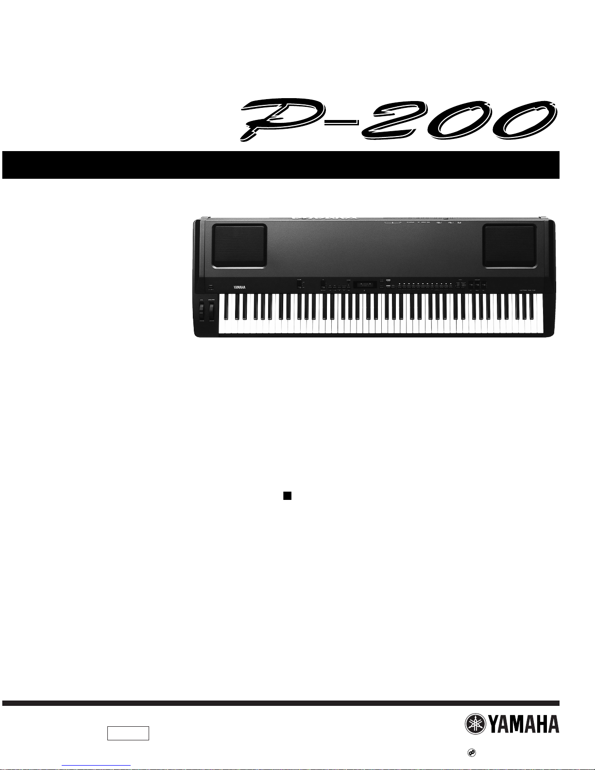
SERVICE MANUAL
ELECTRONIC PIANO
SY
011392
HAMAMATSU, JAPAN
1.96K-759 Printed in Japan '98.03
CONTENTS
CIRCUIT BOARD LAYOUT······························································ 3
BLOCK DIAGRAM·············································································· 4
DISASSEMBLY PROCEDURE························································5
LSI PIN DESCRIPTION··································································· 13
IC BLOCK DIAGRAM······································································ 16
CIRCUIT BOARDS··········································································· 17
TEST PROGRAM············································································· 21
INSPECTIONS·················································································· 23
SPECIFICATIONS ··········································································· 24
PANEL LAYOUT··············································································· 25
ERROR MESSAGES······································································· 26
INITIALIZE························································································· 27
MIDI DATA FORMAT······································································· 28
MIDI IMPLEMENTATION CHART················································· 37
PARTS LIST
OVERALL CIRCUIT DIAGRAM
19980301-198000
P-200
2
WARNING: CHEMICAL CONTENT NOTICE!
The solder used in the production of this product contains LEAD. In addition, other electrical/electronic and/or plastic (where
applicable) components may also contain traces of chemicals found by the California Health and Welfare Agency (and possibly
other entities) to cause cancer and/or birth defects or other reproductive harm.
DO NOT PLACE SOLDER, ELECTRICAL/ELECTRONIC OR PLASTIC COMPONENTS IN YOUR MOUTH FOR ANY REASON
WHAT SO EVER!
Avoid prolonged, unprotected contact between solder and your skin! When soldering, do not inhale solder fumes or expose eyes
to solder/flux vapor!
If you come in contact with solder or components located inside the enclosure of this product, wash your hands before handling
food.
LITHIUM BATTERY HANDLING
This product uses a lithium battery for memory back-up.
WARNING: Lithium batteries are dangerous because they can be exploded by improper handling. Observe the following
precautions when handling or replacing lithium batteries.
Leave lithium battery replacement to qualified service personnel.
Always replace with batteries of the same type.
When installing on the PC board by soldering, solder using the connection terminals provided on the battery cells.
Never solder directly to the cells. Perform the soldering as quickly as possible.
Never reverse the battery polarities when installing.
Do not short the batteries.
Do not attempt to recharge these batteries.
Do not disassemble the batteries.
Never heat batteries or throw them into fire.
ADVARSEL!
Lithiumbatteri-Eksplosionsfare ved fejlagtig håndtering. Udskiftning må kun ske med batteri af samme fabrikat og type. Levér det
brugte batteri tilbage til leverandøren.
VARNING
Explosionsfara vid felaktigt batteribyte.
Använd samma batterityp eller en ekvivalent typ som rekommenderas av apparattillverkaren.
Kassera använt batteri enligt fabrikantens instruktion.
VAROITUS
Paristo voi räjähtää, jos se on virheellisesti asennettu.
Vaihda paristo ainoastaan laitevalmistajan suosittelemaan tyyppiin.
Hävitä käytetty paristo valmistajan ohjeiden mukaisesti.
The following information complies with Dutch Official Gazette 1995. 45; ESSENTIALS OF ORDER ON THE COLLECTION OF
BATTERIES.
•Please refer to the diassembly procedure for the removal of Back-up Battery.
•Leest u voor het verwijderen van de backup batterij deze beschrijving.
IMPORTANT NOTICE
This manual has been provided for the use of authorized Yamaha Retailers and their service personnel. It has been assumed that
basic service procedures inherent to the industry, and more specifically Yamaha Products, are already known and understood by
the users, and have therefore not been restated.
WARNING: Failure to follow appropriate service and safety procedures when servicing this product may result in personal
injury, destruction of expensive components and failure of the product to perform as specified. For these
reasons, we advise all Yamaha product owners that all service required should be performed by an authorized
Yamaha Retailer or the appointed service representative.
IMPORTANT: This presentation or sale of this manual to any individual or firm does not constitute authorization, certification,
recognition of any applicable technical capabilities, or establish a principal-agent relationship of any form.
The data provided is belived to be accurate and applicable to the unit(s) indicated on the cover. The research engineering, and
service departments of Yamaha are continually striving to improve Yamaha products. Modifications are, therefore, inevitable and
changes in specification are subject to change without notice or obligation to retrofit. Should any discrepancy appear to exist,
please contact the distributor's Service Division.
WARNING: Static discharges can destroy expensive components. Discharge any static electricity you body may have
accumulated by grounding yourself to the ground buss in the unit (heavy gauge black wires connect to this
buss.)
IMPORTANT: Turn the unit OFF during disassembly and parts replacement. Recheck all work before you apply power to the
unit.
WARNING
Components having special characteristics are marked and must be replaced with parts having specification equal to those
originally installed.
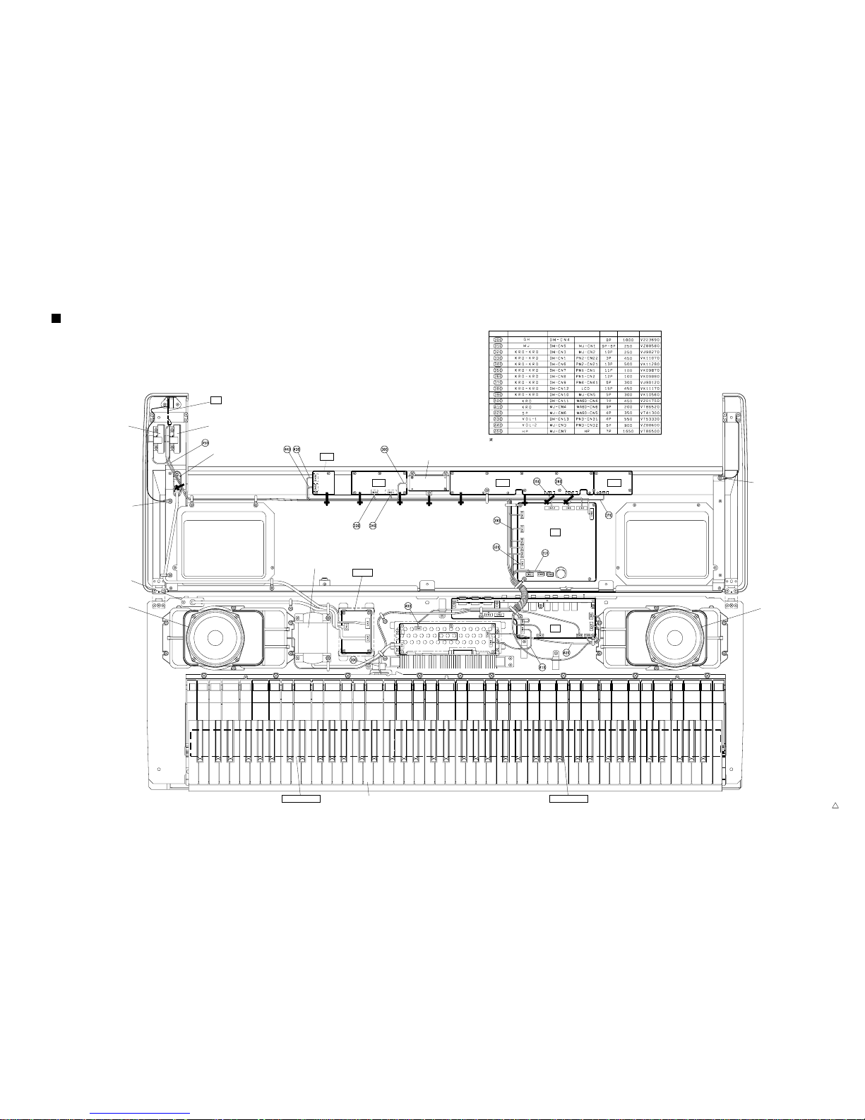
CIRCUIT BOARD LAYOUT
P-200
3
Speaker-L Speaker-R
AC cord
Earth wire
Earth wire
WHEEL1
(PITCH)
WHEEL2
(MODULATION)
HP
GH-D SW L GH-D SW HKeyboard assembly
Power transformer
FU60P
MA60
MJ
DM
PN4PN1PN2
PN3
LCD assembly
POWER switch
Location
Connector Assembly
Destination
Keyboard
Pin L Parts No.
Connector assembly listed above are not available as service parts.
2NC-87520 3/3
3
BLOCK DIAGRAM
P-200
4
DM
PN2
LCD
WHEEL AN4..5
GHD88Key
BEND
LCD
CONT.
CS
SW LED
FRONT PANEL
PN1 PN4
MJ
SW LED
LOW MIDEQHI
IN OUT
MIDI
MIDI
THRU
FC SUS SOS SOFT
REAR PANEL
LINE OUT
L/MONO R L/MONO R
LINE IN
SPEAKER
OFF/ON
SW1
MOD
+5D
FLIP
FLOP
FLIP
FLOP
TR
ARRAY
TR
ARRAY
TA1
TA2
IC14
IC15
IC20
16MHz
FLIP
FLOP
ACK
CN4
CN2
KSN2
LCDCONT
DB0..7
KPB0..2
AN0..2
RXD0
TXD0
AN6
PA2
PA1
PA0
INL
INR
LCDCONT
RESET
SCK1
PA7
RXD1
D8..15
D8..15
KEYBOARD
HP
PN3
MA60
FU60P
AN3
KPB2..3
KPA0..2
KPA0..7
KPB0..3
KPB3
PB0..2
CN1,6 CN12 CN7,8
CN1,2
CN9
CN4
CN5
CN1
CN3
CN7
CN1
PHONES
CN2
CN8
SPEAKER(L)
13cm 30W
SPEAKER(R)
13cm 30W
CN9
CN6
CN2
CN1
CN3
CN1
CN4
CN11
CN10
CN13
CN6
CN6
CN5
CN3
CN32CN31
CN4
CN5
CN4
IC5
POWER AMP
MIX
IC2
IC1
INL
INR
M.VOL
MIX
POWER AMP
Trans Assy
POWER
SUPPLY
POWER SWITCH
AC IN
FUSE
LINE
FILTER
MUTING
CIRCUIT
PB0..7
KPB0.7
CN22,21
-VCC
+VCC
-VCC
+VCC
+50
+B
+5A
-5A
+5A
-5A
+5A
-5A
5V
REG
MUTE
-12
-12
+12
-12
+12
+12
PSRAM
256k
IC12
D8..15
D0..7
A0..14
A0..6
D8..15
A0..5
D8..15
A0..18
A1..18
PA0-2
AN0-7
AN7
D0..15
D0..15
A0..13
D8..15
MT1 MD8
SY1
CKM1
SY0
CKM0
CD
CD
IC13
PSRAM
256k
L
R
LPF
LPF
IC33
IC32
IC30
D/A
20bit
IC1
IC19
IC23
3V
BATTERY
(CR2032)
BATCK
BATCK
BACK
UP
MAIN CPU
H8/3002
XQ375A0
INITIAL
CLEAR
256k
SRAM
IC3
4M
ROM
(DIP)
IC2
IC31
D/A
20bit
DSPNDSPN
EST
IC29
MDA
MI1
DCK
LE
DACL
DACR
CD
GEW9-2
WAVE
ROM
32M
A21
A21
A0..20
D0..15
A0..20
D0..15
IC5
GEW9-2
IC4
IC26
11.2896MHz
IC8
IC9
WAVE
ROM
32M
IC6
IC7
IC11IC10
28CA1-8812237
DISASSEMBLY PROCEDURE
P-200
5
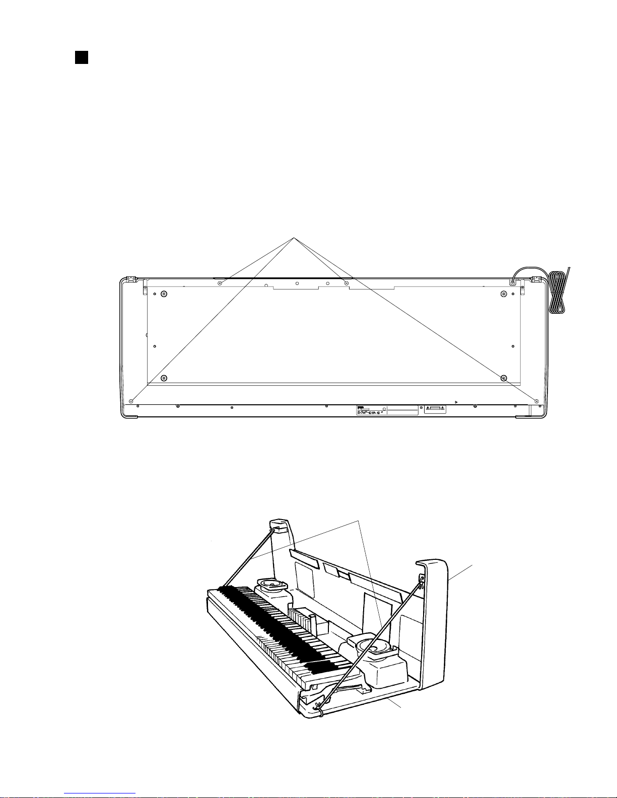
1 Opening Control Panel Unit
Remove the four (4) screws marked [240]
located under the keybed. (Fig. 1)
* Lift the control panel unit from the front and
pass strings through two side plates and both
ends of the keybed, as shown in the figure so
that hinges are not damaged. (Fig. 2)
CAUTION:MAKE SURE THAT THE
UPPER CASE IS SECURE.
[
240
]
[
240
]: Pan Head Screw PW 5.0 x 25 MFZN2BL(VB919400)
(Fig. 1)
(Fig. 2)
Bottom side
Strings
Control panel unit
Keybed

P-200
6
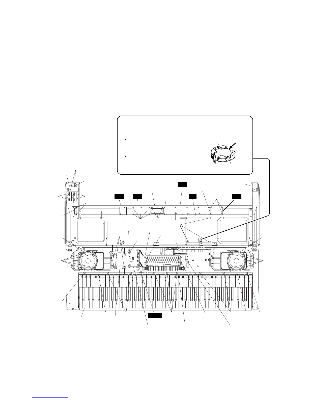
2 DM Circuit Board
2-1 Open the control panel unit. (see procedure 1)
2-2 Remove the four (4) screws marked [920A]. The
DM circuit board can then be removed. (Fig. 3)
* Lithium battery is not a part of DM circuit
board. When you replace the DM circuit
board, remove the lithium battery and install
it in the new circuit board.
3 PN1 Circuit Board
3-1 Open the control panel unit. (see procedure 1)
3-2 Remove the nine (9) screws marked [920B] and
one(1) screw marked [920C]. The PN1 circuit
board can then be removed. (Fig. 3)
4 PN2 Circuit Board
4-1 Open the control panel unit. (see procedure 1)
4-2 Remove the DATA ENTRY knob.
4-3 Remove the five (5) screws marked [920D]. The
PN2 circuit board can then be removed. (Fig. 3)
5 PN3 Circuit Board
5-1 Open the control panel unit. (see procedure 1)
5-2 Remove the VOLUME knob.
5-3 Remove the two (2) screws marked [920E]. The
PN3 circuit board can then be removed. (Fig. 3)
6 PN4 Circuit Board
6-1 Open the control panel unit. (see procedure 1)
6-2 Remove the three EQUALIZER knobs.
6-3 Remove the one(1) screw marked [920C] and
three (3) screws marked [920F]. The PN4 circuit
board can then be removed. (Fig. 3)
7 LCD Assembly
7-1 Open the control panel unit. (see procedure 1)
7-2 Remove the three (3) screws marked [920G]. The
LCD assembly can then be removed. (Fig. 3)
8 MA60 assembly
8-1 Open the control panel unit. (see procedure 1)
8-2 For U.S. model: Before removing the MA60
assembly, it is necessary to remove the MA
cover by removing the four (4) screws marked
[170A]. (Fig. 3)
8-3 Remove the four (4) screws marked [170B]. The
MA60 assembly can then be removed. (Fig. 3)
9 FU60P Circuit Board
9-1 Open the control panel unit. (see procedure 1)
9-2 For U.S. model: Before removing the FU60P
circuit board, it is necessary to remove the FU
cover by removing the four (4) screws marked
[170C]. (Fig. 3)
9-3 Remove the four (4) screws marked [190A]. The
FU60P Circuit Board can then be removed. (Fig. 3)
P-200
7
10 Power Transformer
10-1 Open the control panel unit. (see procedure 1)
10-2 Remove the four (4) screws marked [220]. The
power transformer can then be removed. (Fig. 3)
11 Speakers
11-1 Open the control panel unit. (see procedure 1)
11-2 Remove the four (4) screws marked [4]. The
speaker can then be removed. (Fig. 3)
* The right and left speakers can be removed in
the same manner.
(Fig. 3)
Wheel assembly
HP assembly
[
930B
]
[
930A
]
Power switch
Left speaker
[
930A
]
[
960
]
Right speaker
Control panel unit
[4]
[
200
]
Keyboard assembly
Power transformer
FU cover
[
210
] [
200
] [
200
][
200
][
210
][
200
]
FU60P
MA60 assembly
MA cover
Jack unit
[4]
[
920A
]
[
920G
][
920D
][
920E
]
[
220
]
[
190B
] x 8
[
190A
]
x
4
[
170B
] x 4
[
170A
] x 4
[
920B
] x 9 [
920F
]
[
920C
]
[
170C
] x 4
PN3 PN2 PN4DM
LCD assembly
PN1
[920A-G]: Bind Head Tapping Screw-B 3.0 x 6 MFZN2Y (EP600130)
[170]: Bind Head Tapping Screw-1 3.5 x 12 MFZN2BL (EP030340)
[190]: Bind Head Screw 3.0 x 8 MFZN2Y (VD976600)
[220]: Bind Head Screw 4.0 x 12 MFZN2Y (EG340030)
[4]: Bind Head Tapping Screw-P 4.0 x 30 MFZN2Y (VZ893400)
[930]: Bind Head Tapping Screw-B 3.0 x 8 MFZN2BL (EP600190)
[960]: Bind Head Tapping Screw-B 4.0 x 8 MFZN2Y (EP640410)
Battery VN103500
VN103600(Battery holder for VN103500)
Notice for back-up battery removal
Push the battery as shown in figure,
then the battery will pop up.
Druk de batterij naar beneden zoals
aangeven in de tekening de batterij
springt dan naar voren.
Battery
Battery holder
P-200
8
[
230b
]
[
230b
]: Hexagonal Nut 12 x 14 x 2 MFZN2BL (VB508600)
Earth plate
U-shaped
HP
MJ
(Fig. 4) (Fig. 5)
12 Wheel Assembly
12-1 Open the control panel unit. (see procedure 1)
12-2 Remove the four (4) screws marked [930A]. The
wheel assembly can then be removed. (Fig. 3)
13 Power Switch
13-1 Open the control panel unit. (see procedure 1)
13-2 Remove the two (2) screws marked [960]. The
power switch can then be removed. (Fig. 3)
13-3 Remove the push knob from the power switch.
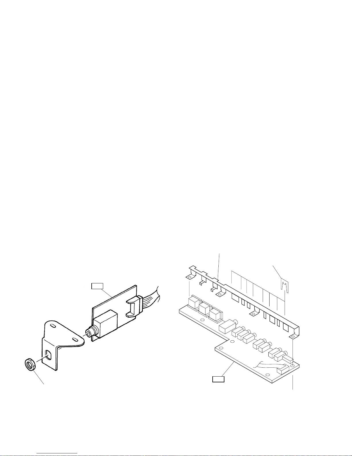
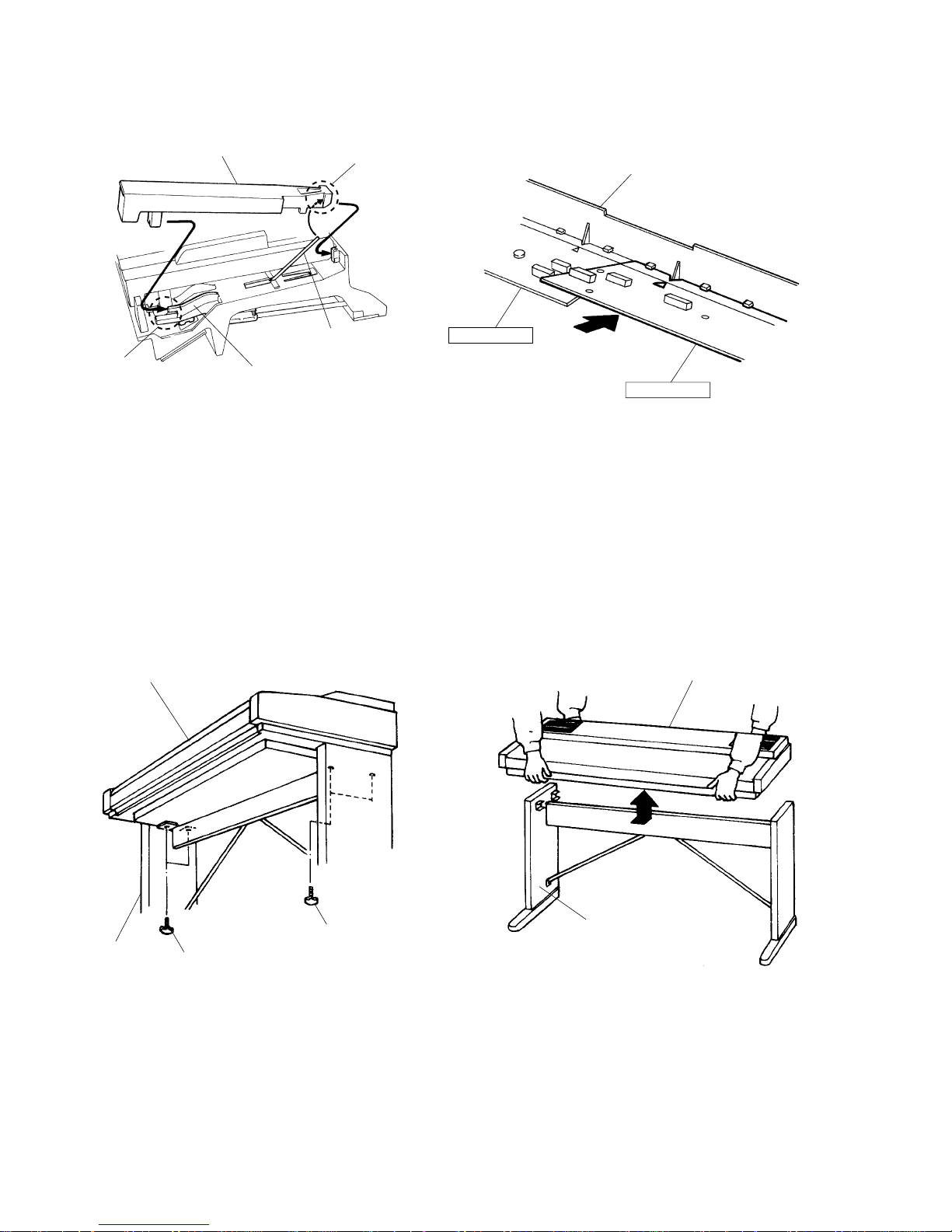
14 HP Circuit Board
14-1 Open the control panel unit. (see procedure 1)
14-2 Remove the two (2) screws marked [930B]. The
HP assembly can then be removed. (Fig. 3)
14-3 Remove the nut marked [230b] and remove the
holder from the HP circuit board. (Fig. 4)
15 MJ Circuit Board
15-1 Open the control panel unit. (see procedure 1)
15-2 Remove the eight (8) screws marked [190B].
The JACK unit can then be removed. (Fig. 3)
15-3 Remove the eight (8) U-shaped holders and
remove the earth plate from the MJ circuit
board. (Fig. 5)
P-200
9
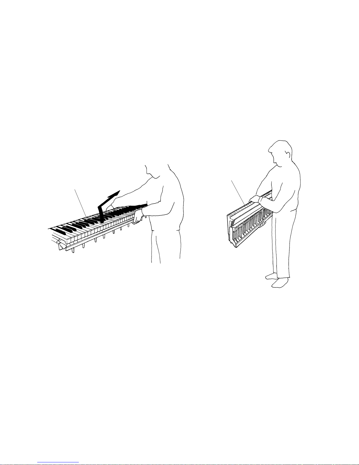
16 Keyboard Assembly
16-1 Open the control panel unit. (see procedure 1)
16-2 Remove the nine (9) screws marked [200] and
two (2) screws marked [210]. The keyboard
assembly can then be removed. (Fig. 3)
* When taking the keyboard assembly out of the
main unit, slide it backward and hold it in the
middle. Lift the keyboard assembly from the
front and take it out of the main unit as shown
in the figures. (Fig. 6 and Fig. 7)
* Do not hold the keyboard by the ends.
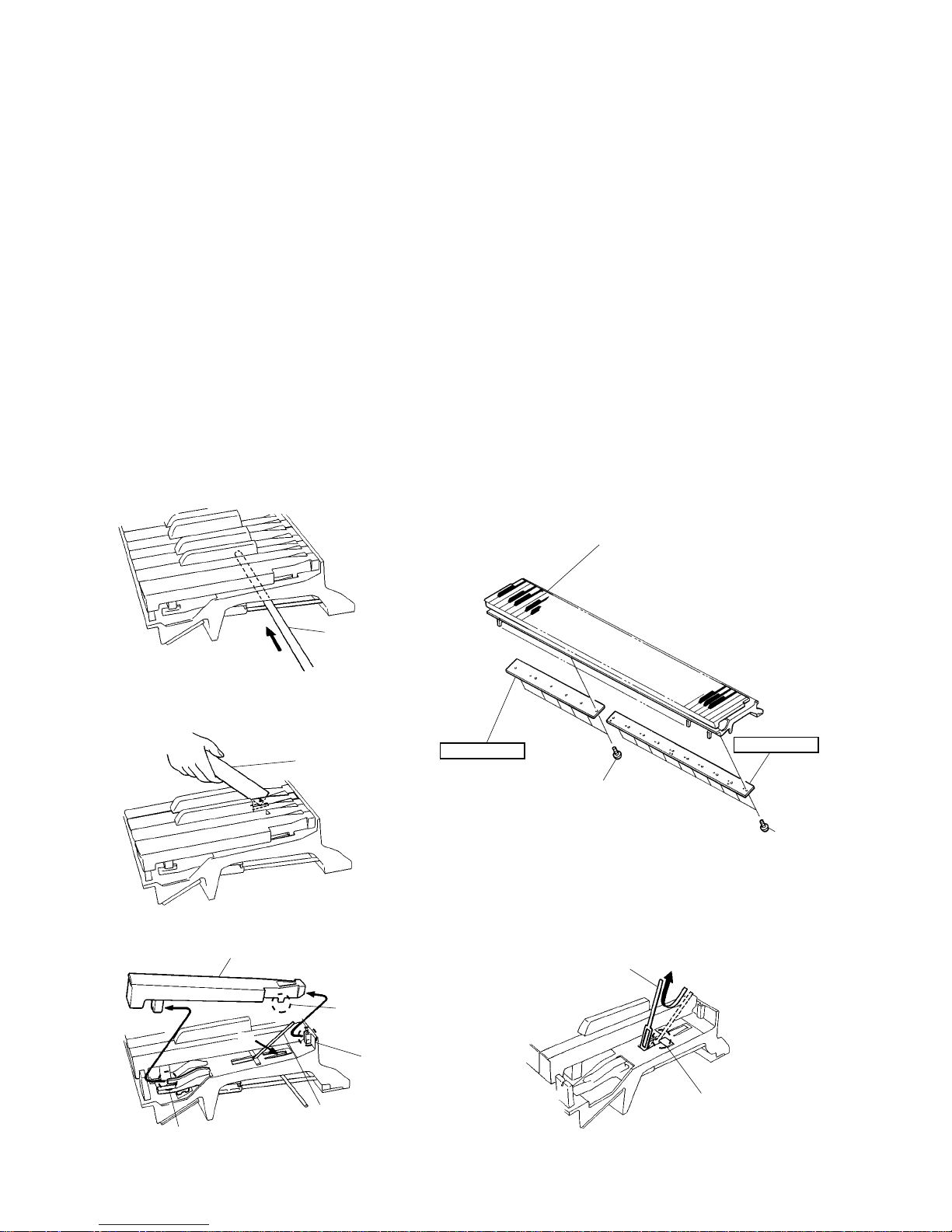
17 Disassembling the Keyboard
* After inserting a round stick (Rod:TX000670)
between the frame and keys, remove the
circuit boards. (Fig. 8)
17-A Take the keyboard assembly out of the main
unit. (see procedure 16)
17-B Remove the GH-D SW (L) circuit board by
removing the seven (7) screws marked [260A].
(Fig. 9)
17-C Remove the GH-D SW (H) circuit board by
removing the ten (10) screws marked [260B].
(Fig. 9)
* Keys can be removed without removing the
circuit boards.
* After removing the GH-D SW (L) and GH-D
SW (H) circuit boards, and the rubbers can
then be removed.
(Fig. 6) (Fig. 7)
Keyboard assembly
Keyboard assembly
P-200
10
17-D Insert a thin plate between the white keys, near
the triangle mark around the fulcrum of the key,
and press down the stopper marked [A] to
remove the key. (Fig. 8, Fig. 10 and Fig. 11)
* Take care not to damage the key spring when
removing a key.
* A black key can be removed after the white
keys on either side have been removed.
17-E After a key has been removed, push a key spring
down once to take it out of the hook. (Fig. 12)
Place the keyboard assembly upside-down and
peel the stopper away. Then hammer of the
white key can then be removed. (Fig. 13)
(Fig. 11) (Fig. 12)
(Fig. 9)(Fig. 10)
(Fig. 8)
[
260A
]
[C]
[D]
[B]
[
260B
]
[
260
]: Bind Head Tapping Screw-P 3.0 x 10 MFZN2Y
(VT413400)
Keyboard assembly
White key
Thin metal plate etc
GH-D SW(L)
GH-D SW(H)
Insert a round
stick before removing
circuit boards.
Spring
Spring
Hook
[A]
Rod (TX000670)
P-200
11
18 Assembling the Keybed
18-A Place the keyboard assembly upside-down,
insert a hammer assembly into the frame, and
put the stopper on. (Fig. 14)
* There are four (4) weights of hammers.
18-B Place the keyboard assembly rightside up. Fix
key springs on the frame by setting one at each
slit and pushing down once on each key?
spring?. (Fig. 14 and Fig. 15)
* Be careful of the direction of the spring.
18-C After a key has been fit to part [F] and key
guide, make sure that the spring is fixed to the
key and then press down part [E] of the key.
(Fig. 16)
18-D Tighten the seven (7) screws marked [260A] to
fix the GH-D SW (L) circuit board. (Fig. 9)
18-E Tighten the ten (10) screws marked [260B] to
fix the GH-D SW (H) circuit board. (Fig. 9)
* Install the circuit boards in the keyboard
assembly so that the hooks hold it as shown in
figure 17.
(Fig. 13)
Hammer, white key
Stopper (L88)
(Fig. 14) (Fig. 15)
Spring
Frame
Frame
Hook
Hammer, white key
Stopper (L88)
up
P-200
12
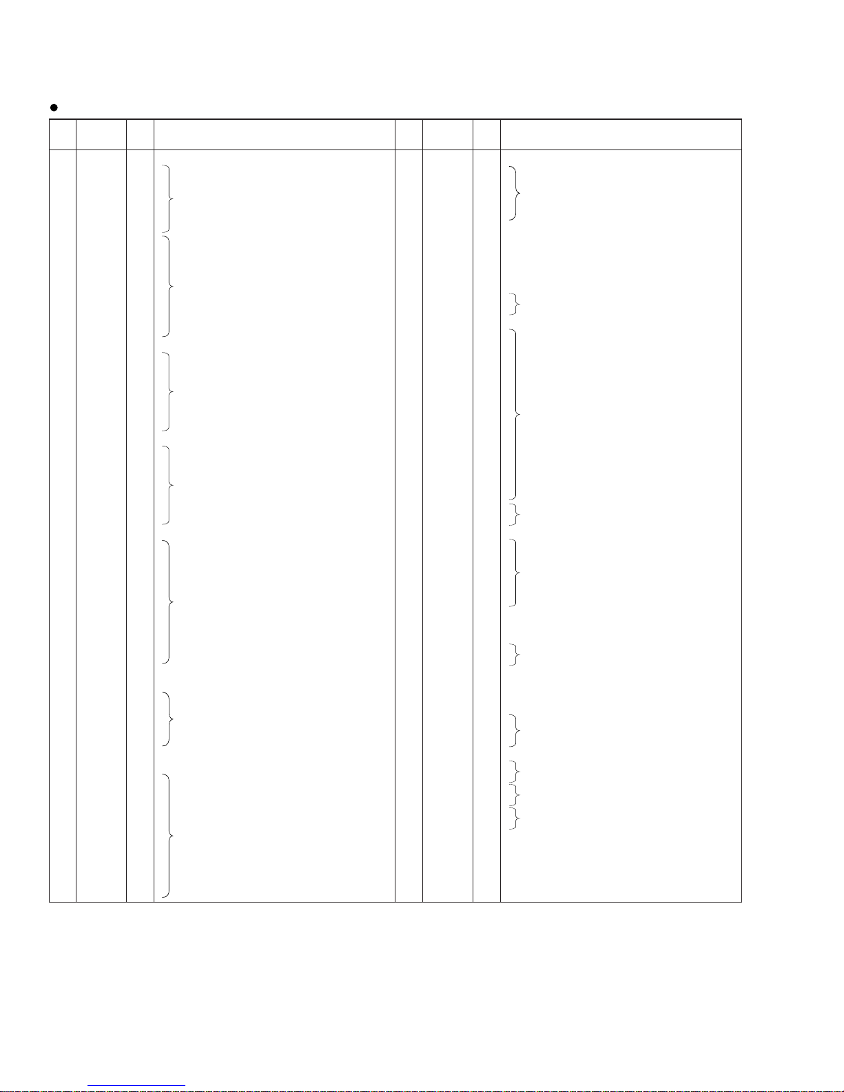
19 Main Unit
19-1 Remove the four (4) knob bolts. (Fig. 18)
19-2 Then, carefully lift the main unit up from the
side boards and slide it toward the back. Next,
raise it, taking care not to pinch your fingers.
(Fig. 19)
CAUTION: WATCH YOUR FINGERS
WHEN DOING THIS!!
(Fig. 16) (Fig. 17)
Keyboard assembly : bottom side
White key
[E]
Spring
Key guide
[F]
GH-D SW(L)
GH-D SW(H)
(Fig. 18) (Fig. 19)
Knob bolt
Knob bolt
P-200 P-200
Key board stand
LP-3
Key board stand
LP-3

LSI PIN DESCRIPTION
P-200
13
PIN
NO.
1
2
3
4
5
6
7
8
9
10
11
12
13
14
15
16
17
18
19
20
21
22
23
24
25
26
27
28
29
30
31
32
33
34
35
36
37
38
39
40
41
42
43
44
45
46
47
48
49
50
I/O
O
O
I
I
I
I
I
I
I
I
O
O
O
I
I
O
I
I/O
I/O
I/O
I/O
I/O
I/O
I/O
I/O
I/O
I/O
I/O
I/O
I/O
I/O
I/O
I/O
O
O
O
O
O
O
O
O
O
O
O
O
PA6
PA7
VCC
PB0
PB1
PB2
PB3
PB4
PB5
PB6//DREQ0
PB7//DREQ1
/RESO
VSS
P90/TXD0
P91/TXD1
P92/RXD0
P93/RXD1
P94/SCK0
P95/SCK1
P40/D0
P41/D1
P42/D2
P43/D3
VSS
P44/D4
P45/D5
P46/D6
P47/D7
D8
D9
D10
D11
D12
D13
D14
D15
VCC
A0
A1
A2
A3
A4
A5
A6
A7
VSS
A8
A9
A10
A11
NAME
Port A
Address bus
Power supply
Port B
Reset
Ground
Transmit data (MIDI OUT)
KSN-ACK
Receive data (MIDI IN)
KSN-RX
Port 9
Port 9
(Ground)
Data bus
Power supply
Address bus
(Ground)
FUNCTION
PIN
NO.
51
52
53
54
55
56
57
58
59
60
61
62
63
64
65
66
67
68
69
70
71
72
73
74
75
76
77
78
79
80
81
82
83
84
85
86
87
88
89
90
91
92
93
94
95
96
97
98
99
100
I/O
O
O
O
O
O
O
O
O
I
I
I
O
I
I
I
I
O
O
O
O
O
I
I
I
I
I
I
I
I
I
I
I
I
O
O
O
O
O
I
I
I
O
O
O
A12
A13
A14
A15
A16
A17
A18
A19
VSS
P60//WAIT
P61//BREQ
P62//BACK
Ø
/STBY
/RES
NMI
VSS
EXTAL
XTAL
VCC
/AS
/RD
/HWR
/LWR
MD0
MD1
MD2
AVCC
VREF
P70/AN0
P71/AN1
P72/AN2
P73/AN3
P74/AN4
P75/AN5
P76/AN6
P77/AN7
AVSS
P80
P81//CS3
P82//CS2
P83//CS1
P84//CS0
VSS
PA0
PA1
PA2
PA3
PA4
PA5
NAME
Address bus
Ground
Port 6
Øout
Stand-by mode signal
Reset
Non-maskable interrupt
Ground
Clock
Clock
Power supply
Address strobe
Read strobe
Write strobe (High)
Write strobe (Low)
Mode select
Analog power supply
Reference voltage
Analog data input (EQ)
Analog input (EQ)
Analog data input
Analog input (CS)
Analog data input (BEND)
Analog input (MOD)
Analog input (FC)
Analog input (BAT)
Analog ground
Port 8
Chip select
Ground
Port A
FUNCTION
PIN
NO.
1
2
3
4
5
6
7
8
9
10
11
12
13
14
15
16
17
18
19
20
I/O
O
O
O
O
O
O
I
I
I
I
I
I
I
I
I
I
I
I
I
O
BK5
BK4
BK3
BK2
BK1
BK0
MK15
MK14
MK13
MK12
MK11
MK10
MK05
MK04
MK03
MK02
MK01
MK00
XIN
XOUT
NAME
Key block (open drain)
1st make contact
2nd make contact
Crystal osc. input (4 MHz)
Crystal osc. output (4 MHz)
FUNCTION
PIN
NO.
21
22
23
24
25
26
27
28
29
30
31
32
33
34
35
36
37
38
39
40
I/O
O
I
I
I
I
I
I
O
O
O
O
O
O
O
O
O
GND
VDD
SO
ACK
XCK
/IC
TST1
TST2
XCKINH
BK14
BK13
BK12
BK11
BK10
BK9
BK8
BK7
BK6
GND
VDD
NAME
Ground
Power supply
Serial data
Acknowledge/Mode select
Clock for serial data
Initial clear
Test mode
(L, L: normal mode, others: test)
Inhibit of serial clock
Key block (open drain)
Ground
Power supply
FUNCTION
HD6413002FP16 (XQ375A00) CPU <H8/3002>
YMZ702-D (XR632A00) KSN2 (Key Scanner)
P-200
14
PIN
NO.
1
2
3
4
5
6
7
8
9
10
11
12
13
14
15
16
17
18
19
20
21
22
23
24
25
26
27
28
29
30
31
32
33
34
35
36
37
38
39
40
41
42
43
44
45
46
47
48
49
50
51
52
53
54
55
56
57
58
59
60
61
62
63
64
I/O
I
I
I
I
I
I
I/O
I/O
I/O
I/O
I/O
I/O
I/O
I/O
I/O
I/O
I/O
I/O
I/O
I/O
I/O
I/O
O
O
O
O
O
O
O
O
O
O
O
O
O
O
O
O
O
O
O
I
O
O
O
O
O
O
O
I/O
I/O
I/O
I/O
I/O
I/O
I/O
I/O
I/O
I/O
I/O
Vss
A0
A1
A2
A3
A4
A5
D0
D1
D2
D3
D4
D5
D6
D7
D8
Vss
D9
D10
D11
D12
D13
D14
D15
/IRQ
MA0
MA1
MA2
MA3
MA4
MA5
MA6
Vss
MA7
MA8
MA9
MA10
MA11
MA12
MA13
MA14
MA15
MA16
MA17
MAE
V
DD
MA18
MA19
MA20
MA21
MA22
/MWR
BDIR
MD0
MD1
MD2
MD3
MD4
MD5
MD6
MD7
MD8
MD9
MD10
NAME
Ground
Address bus
Data bus
Ground
Data bus
Interrupt request
External memory address bus
Ground
External memory address bus
Memory address enable
Power supply
External memory address bus
Memory write control
Data bus direction
External memory data bus
FUNCTION
YMW259 (XJ752C00) GEW9-F (AWM Tone Generator & Digital Filter)
PIN
NO.
65
66
67
68
69
70
71
72
73
74
75
76
77
78
79
80
81
82
83
84
85
86
87
88
89
90
91
92
93
94
95
96
97
98
99
100
101
102
103
104
105
106
107
108
109
110
111
112
113
114
115
116
117
118
119
120
121
122
123
124
125
126
127
128
I/O
I/O
I/O
I/O
I/O
I/O
I
I
O
I
O
O
I
O
O
O
O
O
O
O
O
O
O
O
O
O
O
O
O
O
O
O
O
O
O
O
O
O
O
I
I
O
O
O
O
O
O
O
I
I
O
O
O
O
I
I
I
I
O
I
Vss
MD11
MD12
MD13
MD14
MD15
/IC
SYI
SYO
CKMI
CKMO
V
DD
XOUT
XIN
Vss
RA0
RA1
RA2
RA3
RA4
RA5
RA6
RA7
RA8
RA9
RA10
RA11
RA12
RA13
RA14
RD0
RD1
Vss
RD2
RD3
RD4
RD5
RD6
RD7
/CE
/OE
/WE
TP1
TP0
DCK
LE
MCK64
MCK32
MOA
MOB
MOC
V
DD
MI1
MI2
DRA
DRB
DLA
DLB
/CS
/RD
/WR
8/16
CDO
A-1
NAME
Ground
External memory data bus
Initial clear
Synch. pulse input
Synch. pulse output
Clock 12.8 MHz input
Clock 12.8 MHz output
Power supply
Clock
Ground
not used
not used
Ground
not used
Chip enable
Output enable
Write enable
Test pin
DAC clock
Latch enable
Clock 6.4 MHz output
Clock 3.2 MHz output
MEL format data output
Power supply
MEL format data input
R-channel serial data output
L-channel serial data output
Chip select
Read control
Write control
Bus width 8 bit/16 bit
Control data output
Address bus
FUNCTION
P-200
15
PIN
NO.
1
2
3
4
5
6
7
8
9
10
11
12
13
14
15
16
17
18
19
20
21
22
23
24
25
26
27
28
29
30
31
32
I/O
I/O
I/O
I/O
I/O
I/O
I/O
I/O
I/O
I/O
I/O
I
I
O
O
I
I
O
I
O
I
O
I
O
O
O
O
O
O
O
O
MDAT9
MDAT8
MDAT7
MDAT6
MDAT5
MDAT4
MDAT3
MDAT2
MDAT1
Vss
MDAT0
SI1
SI0
SO1
SO0
XMD
XCLK
/TO
/CRS
CDO
CDI
TIM1
/OE
R/W
MAD15
V
DD
MAD14
MAD13
MAD12
MAD11
MAD10
MAD9
NAME
External RAM data bus
(Ground)
Data input
Data output
ACIA synch. mode
ACIA clock
Timer output
CDI reset
Command output
Command input
Timer 1
Output enable
Read/write
(Power supply)
External RAM address bus
FUNCTION
PIN
NO.
33
34
35
36
37
38
39
40
41
42
43
44
45
46
47
48
49
50
51
52
53
54
55
56
57
58
59
60
61
62
63
64
I/O
O
O
O
O
O
O
O
O
O
I
I
O
I
I
O
I
O
O
O
O
I
I
O
O
I/O
I/O
I/O
I/O
I/O
I/O
MAD8
MAD7
MAD6
MAD5
MAD4
MAD3
MAD2
MAD1
MAD0
Vss
/TSTR
/TST1
CLKM
SYW
CLK
/CE
/IC
MDTS4
MDTS3
MDTS2
MDTS1
MDSI1
MDSI0
MDSO1
MDSO0
V
DD
MDAT15
MDAT14
MDAT13
MDAT12
MDAT11
MDAT10
NAME
External RAM address bus
Ground
Test R
Test 1
1/2 clock
Synch. signal input
Clock
External RAM chip enable
Initial clear
MOD data test
Wave add data input
Wave add data input
Power supply
External RAM data bus
FUNCTION
PIN
NO.
1
2
3
4
5
6
7
8
9
10
I/O
I
I
I
DATA
CLK
NC
+VDD
D.COM
-VDD
L.E
NC
NC
NC
NAME
Data input
Clock
Power supply (+5 V) Digital
Digital ground
Power supply (-5 V) Digital
Latch enable
FUNCTION
PIN
NO.
11
12
13
14
15
16
17
18
19
20
I/O
I/O
O
I/O
I/O
+VCC
BPO-DC
NC
LOUT
A.COM2
A.COM1
SERVO-DC
NC
REF-DC
-VCC
NAME
Power supply (+5 V)
Bipolar de-couple
Output current
Analog ground
Analog ground
Servo de-couple
Reference de-couple
Power supply (-5 V)
FUNCTION
YSS208 (XI816A00) DSPN (Digital Signal Processor)
PCM1702U (XP551A00) DAC (Digital to Analog Converter)
PIN
NO.
1
2
3
4
5
6
7
8
I/O
I
O
I
I
I
O
Vss
SI0
SO0
BC0
WC0
SI2
SO2
Vdd
NAME
Ground
Serial data input 0
Serial data output 0
Bit clock channel 0
Word clock channel 0
Serial data input 2
Serial data output 2
Power supply
FUNCTION
PIN
NO.
9
10
11
12
13
14
15
16
I/O
I
I
I
I
I
I
O
I
M0
M1
M2
M3
WC1
BC1
SO1
SI1
NAME
Mode select
Word clock channel 1
Bit clock channel 1
Serial data output 1
Serial data input 1
FUNCTION
YM3422B (XE862B00) ES1 (Format Converter)

P-200
16
IC BLOCK DIAGRAM
Q
DCK
OE
Q
DCK
OE
Q
DCK
OE
Q
DCK
OE
OUTPUT
CONTROL
1Q
1D
2D
2Q
3Q
3D
4D
4Q
GND
1 20
2 19
3 18
4 17
5 16
6 15
7 14
8 13
9 12
10 11
HD74AC32FPEL (XK452A00)
Quad 2 Input OR
SN74HC132NSR (XL112A00)
Quad 2 Input NAND
1
2
31A1Y
42A
52B
62Y
7GND
1B
14
13
12
Vcc
4A
11 4Y
10 3B
93A
83Y
4B
1
2
31A1Y
42Y
52A
62B
7GND
1B
14
13
12
VDD
4A
11 4Y
10 3Y
93B
83A
4B
SN74HC139NSR (XC727A00)
Dual 2 to 4 Demultiplexer
1
2
3
4
5
6
7
1G
1A
1B
1Y0
1Y1
1Y2
1Y3
A
G
B
Y0
Y1
Y2
Y3
16
15
14
13
12
11
10
Vcc
2G
2A
2B
2Y0
2Y1
2Y2
8
GND
9
2Y3
Y2
Y3
Y1
Y0
B
A
G
µ PC4570HA (XB247A00)
Dual Operational Amplifier
SN74HC374ANSR (XQ042A00)
Octal 3-State D-FF
µ PC4570G2 (XF291A00)
Dual Operational Amplifier
TC7S04F (XM182A00)
Inverter Gate
VCC
8Q
8D
7D
7Q
6Q
6D
5D
5Q
CLOCK
Q
DCK
OE
Q
DCK
OE
Q
DCK
OE
Q
DCK
OE
1
2
3
5
4
NC
GND
Vcc
OUT Y
IN A
1A2 3 4 5 6 7 8 9
+V -IN -V
+INOUT
AAA
+V-IN
+IN OUT
BBB
-
+
B
-
+
1
2
3
4-V
8
7
6
5
Output A +V
Non-Inverting
Input A
-DC Voltage Supply
+DC Voltage
Supply
Output B
Inverting
Input B
Non-Inverting
Input B
Inverting
Input A
+-
+-
to LCD assembly
to MA60-CN4 to MJ-CN1 to Keyboard
Component side Pattern side
to PN2-CN21 to PN1-CN1
to PN1-CN2
to PN3
-CN31
to MJ
-CN5
to MJ
-CN2
to PN4
-CN41
to PN2
-CN22
to Wheel
assembly
2NA-VZ88550
1
CIRCUIT BOARDS
P-200
17
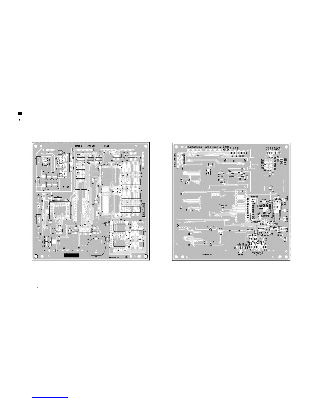
DM Circuit Board
Note : See parts list for details of circuit board
component parts.
STORE PERF. A to DM-CN7 to DM-CN8
CS
DATA ENTRY
PS1
-1/NO
PS2
+1/YES
SPLIT
BALANCE
TRANSPOSE
DETUNE
MIDI
PAGE
CONTRAST
to DM-CN1 to DM-CN6
VOLUME to DM-CN9 EQUALIZER
to DM-CN13
to MJ-CN3
Component side
Component side Component side
Component side
2NA-VT36040
0
EDIT PREF. B VOICE PIANO1
SYSTEM
PIANO2
MIDI FILTER
PIANO3
PC TABLE
PIANO4
CHANNEL
E. PIANO1
LOCAL
E. PIANO2
CS FC
E. PIANO3PSVIBES
NAME
ORGAN1
ORGAN
COMBINATION
ORGAN2
PB MW
STRINGS
KBD SENS
BASS
INT.EQ
REVERB
EFFECT
ROOM
CHORUS
SYMPHONIC
TREMOLO
STAGE
HALL
MODULATION
LOW MIDDLE HIGH
anode cathode
P-200
18
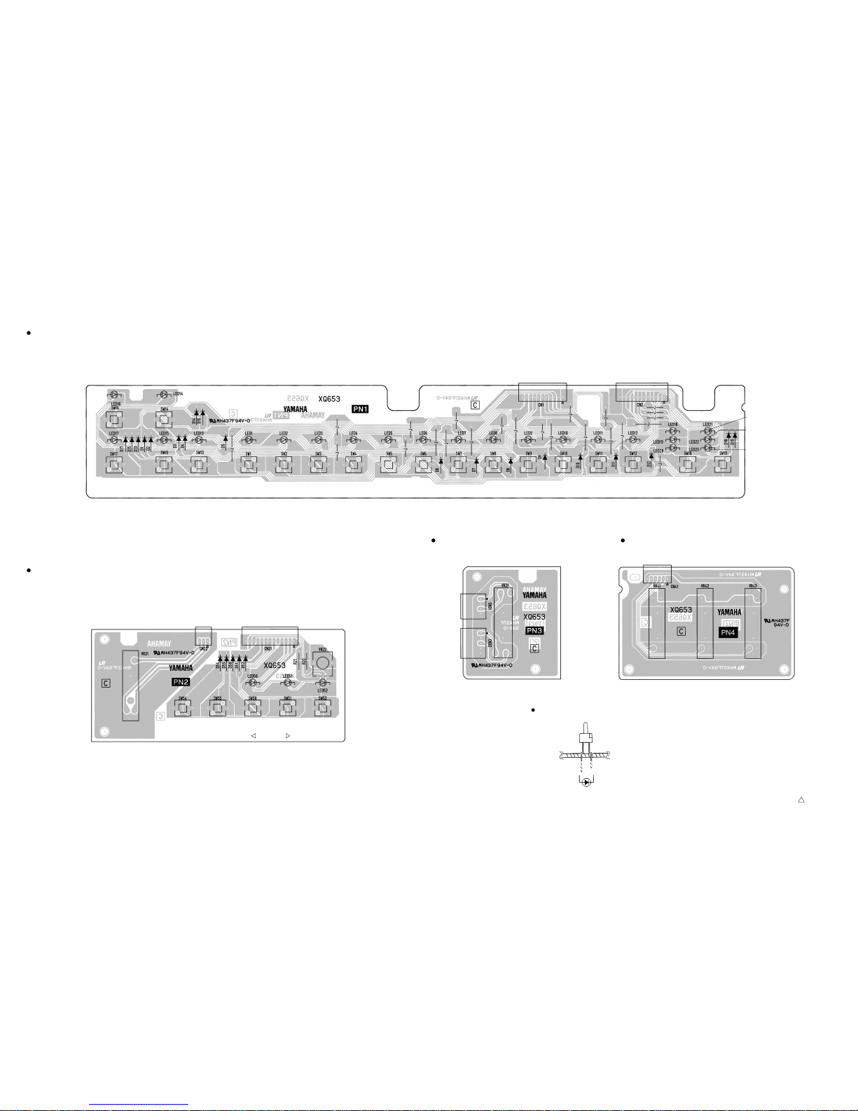
PN1 Circuit Board
PN2 Circuit Board
PN3 Circuit Board PN4 Circuit Board
LED installing
Note : See parts list for details of circuit board
component parts.
P-200
19
PHONES
Earth wire
VG60540
to MJ-CN7
Component side
Component side
HP : 2NA-VT83360
MJ : 2NA-VT35990
0
IN OUT
MIDI
THRU FOOT CONTROLLER SOFT SOSTENUTO SUSTAIN
to DM-CN3to DM-CN5
to MA60-CN6
to DM-CN10
to SP-Rto SP-Lto PN3-CN32
to MA60-CN5
to HP-CN1
L/MONO
OUTPUT
R L/MONO
INPUT SPEAKER
R ON OFF
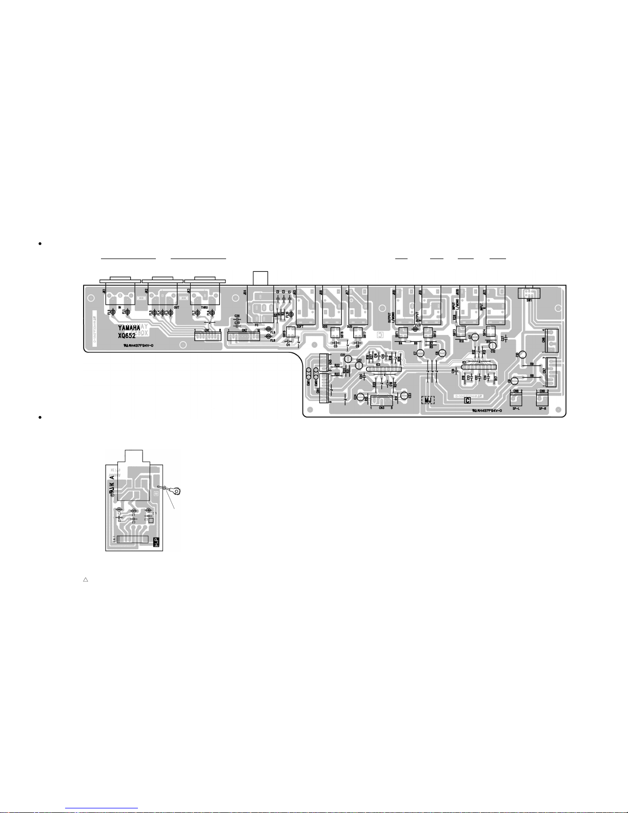
MJ Circuit Board
HP Circuit Board
Note : See parts list for details of circuit board
component parts.
P-200
20
Component sideComponent side
MA60 : 2NA-VT14420
1
FU60P : 2NA-VT45890
0
to Power Transformer
secondary
to Power Transformer Primary to POWER SW
R1, R2, C2, C14, C15, DB3: not installed to DM-CN11 AC IN
to MJ-CN4
to MJ-CN6
CAUTION: REPLACE WITH SAME TYPE
5A 125V FUSE.
ATTENTION: UTILISER UN FUSIBLE DE
RECHANGE DE MÉME TYPE DE 5A 125V
NOTE : The symbol ( ) shows Slow operating fuse.
5A 125V
STK401-XXX
Insulation sheet (VJ834500)
IC1
IC5
TR1IC3.4
VT740000
Spacers
VT443500
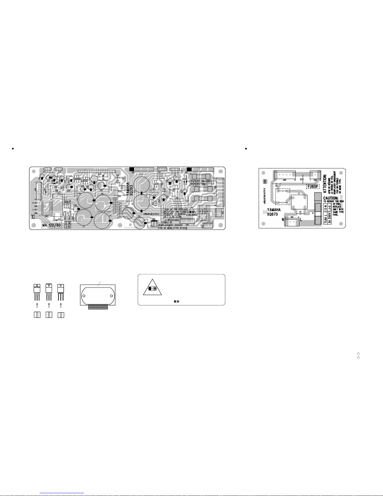
MA60 Circuit Board FU60P Circuit Board
Note : See parts list for details of circuit board
component parts.