

Page 1
RX-V461/HTR-6040/
DSP-AX461
AV RECEIVER/AV AMPLIFIER
RX-V461/HTR-6040/DSP-AX461
SERVICE MANUAL
For U, C, R, K, A, L and J models
This service manual is the RX-V461/HTR-6040/DSP-AX461 (U, C, R, K, A, L and J models).
For service manual of the RX-V461/RX-V461DAB (T, B, G and E models), please refer to the following publication number:
RX-V461/RX-V461DAB (T, B, G and E models): 101048
This manual has been provided for the use of authorized YAMAHA Retailers and their service personnel.
It has been assumed that basic service procedures inherent to the industry, and more specifically YAMAHA Products, are already
known and understood by the users, and have therefore not been restated.
WARNING: Failure to follow appropriate service and safety procedures when servicing this product may result in personal
injury, destruction of expensive components, and failure of the product to perform as specified. For these reasons,
we advise all YAMAHA product owners that any service required should be performed by an authorized
YAMAHA Retailer or the appointed service representative.
IMPORTANT: The presentation or sale of this manual to any individual or firm does not constitute authorization, certification or
recognition of any applicable technical capabilities, or establish a principle-agent relationship of any form.
The data provided is believed to be accurate and applicable to the unit(s) indicated on the cover. The research, engineering, and
service departments of YAMAHA are continually striving to improve YAMAHA products. Modifications are, therefore, inevitable
and specifications are subject to change without notice or obligation to retrofit. Should any discrepancy appear to exist, please
contact the distributor's Service Division.
WARNING: Static discharges can destroy expensive components. Discharge any static electricity your body may have
accumulated by grounding yourself to the ground buss in the unit (heavy gauge black wires connect to this buss).
IMPORTANT: Turn the unit OFF during disassembly and part replacement. Recheck all work before you apply power to the unit.
■ CONTENTS
TO SERVICE PERSONNEL .......................................... 2
FRONT PANELS ........................................................ 3–4
REAR PANELS .......................................................... 4–7
REMOTE CONTROL PANELS ...................................... 8
SPECIFICATIONS / 参考仕様 .................................. 9–11
INTERNAL VIEW ......................................................... 12
DISASSEMBLY PROCEDURES / 分解手順.......... 12–14
UPDATING FIRMWARE/
ファームウェアの書き込み..................................... 15–17
SELF DIAGNOSIS FUNCTION (DIAG)/
自己診断機能(ダイアグ)..................................... 18–36
IMPORTANT NOTICE
DISPLAY DATA ........................................................... 37
IC DATA ................................................................. 38–52
BLOCK DIAGRAMS .............................................. 53–54
PIN CONNECTION DIAGRAMS .................................. 55
PRINTED CIRCUIT BOARDS................................ 56–68
SCHEMATIC DIAGRAMS ...................................... 69–80
REPLACEMENT PARTS LIST .............................. 81–95
REMOTE CONTROL.............................................. 96–99
Advanced setup / すべての設定を初期設定に戻す..... 100
101041
2007 All rights reserved.
This manual is copyrighted by YAMAHA and may not be copied or
redistributed either in print or electronically without permission.
P.O.Box 1, Hamamatsu, Japan
'07.02
Page 2
■ UPDATING FIRMWARE / ファームウェアの書き込み
RX-V461/HTR-6040/
DSP-AX461
RX-V461/HTR-6040/DSP-AX461
After replacing the following parts with the replacement part,
be sure to write the latest firmware.
• DSP P.C.B.
• IC201 (DSP P.C.B.)
● Required Tools
• DVD or CD player (with DIGITAL OUTPUT (OPTICAL
or COAXIAL) terminal)
• Optical cable (when OPTICAL terminal is used)
• Digital audio pin cable (when COAXIAL terminal is
used)
• Firmware CD
* To make the firmware CD, download the latest firm-
ware from the specified download source to PC.
● Operation Procedures
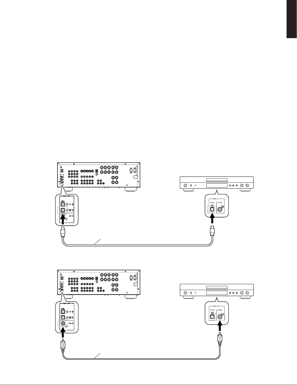
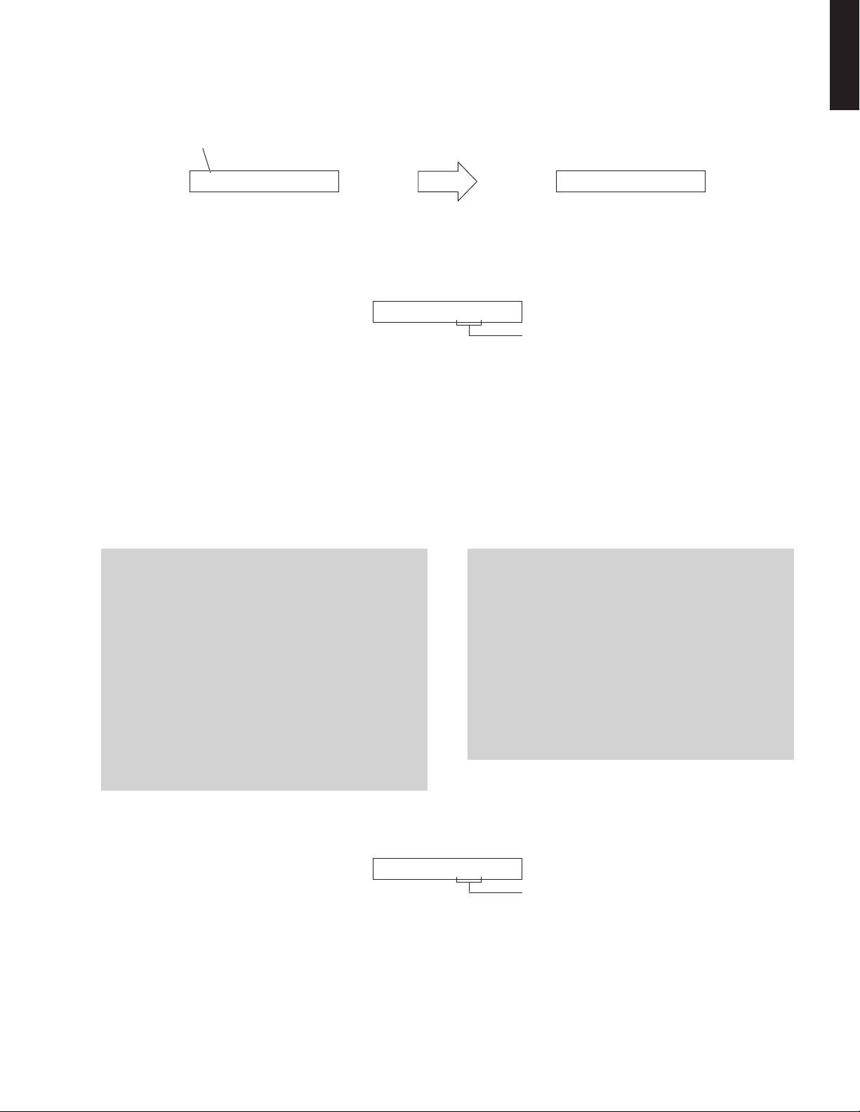
1. Connect the main unit and DVD/CD player as shown
below. (Fig. 1)
Example of OPTICAL terminal / OPTICAL端子使用例
Main unit
本機
下記部品をサービス部品に交換した場合、最新のファーム
ウェアの書き込みを行ってください。
・ DSPP.C.B.
・ IC201(DSPP.C.B.)
● 必要なツール
・ DVDまたはCDプレーヤー(DIGITALOUTPUT
(OPTICALまたはCOAXIAL)端子付き)
・ 光ファイバーケーブル(OPTICAL端子使用時)
・ デジタル音声ピンケーブル(COAXIAL端子使用時)
・ ファームウェアCD
※ ファームウェアCDは、PCへ最新のファーム
ウェアを指定のダウンロード先からダウンロー
ドして制作してください。
● 操作方法
1. 本機とDVD/CDプレーヤーを下記のように接続しま
す。(Fig.1)
DVD/CD player
DVD/CDプレーヤー
Optical cable
光ファイバーケーブル
Example of COAXIAL terminal / COAXIAL端子使用例
Main unit
本機
Digital audio pin cable
デジタルピンケーブル
Fig. 1
DVD/CD player
DVD/CDプレーヤー
15
Page 3
RX-V461/HTR-6040/DSP-AX461
DSP-AX461
RX-V461/HTR-6040/
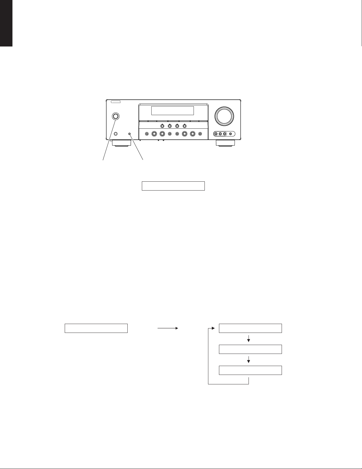
2. While pressing the “STANDBY/ON” key and “SPEAKERS A/B/OFF” key of the main unit simultaneously,
connect the power cable of the main unit to the AC
outlet. (Fig. 2)
The FIRMWARE UPDATE mode will then be activated and “SPDIF Upgrade” is displayed. (Fig. 2)
2. 本機のSTANDBY/ONキーと、SPEAKERSA/B/
OFFキーを押しながら、本機の電源コードをACコ
ンセントに接続します。(Fig.2)
FIRMWAREUPDATEモードが起動し、SPDIF
Upgradeが表示されます。(Fig.2)
"STANDBY/ON" key
"SPEAKERS A/B/OFF" key
FIRMWARE UPDATE mode
SPDIF Upgrade
3. Connect the power cable of DVD/CD player to the
AC outlet.
4. Press the “STANDBY/ON” key of the DVD/CD player.
5. Press the “EJECT” key of the DVD/CD player to open
the tray.
6. Put the firmware CD on the tray and close the tray.
7. Press the “PLAY” key of the DVD/CD player.
Then writing of the firmware is started. (Fig. 3)
8. When writing of the firmware is completed, “Upgrade OK”, “Please...” and “Turn off!!” are displayed repeatedly. (Fig. 3)
Address:XXXXXX Upgrade OK
XXXXXX: Address information of the received data /
受信データのアドレス情報
Fig. 2
3. DVD/CDプレーヤーの電源コードをACコンセント
に接続します。
4. DVD/CDプレーヤーのSTANDBY/ONキーを押し
ます。
5. DVD/CDプレーヤーのEJECTキーを押し、トレー
を開きます。
6. ファームウェアCDをトレーに載せ、トレーを閉じ
ます。
7. DVD/CDプレーヤーのPLAYキーを押します。
ファームウェアの書き込みが開始されます。(Fig.3)
8. ファームウェアの書き込み完了後、Upgrade
OK、Please...、Turnoff!!が繰り返し表示され
ます。(Fig.3)
Writing is completed. / 書き込み完了Writing is started. / 書き込み開始
Please...
16
Turn off!!
Fig. 3
Page 4

RX-V461/HTR-6040/DSP-AX461
RX-V461/HTR-6040/
DSP-AX461
* When the version of the firmware to be written
is the same as the one existing in the main unit,
“Same Version”, “Please...” and “Turn off!!” are
displayed repeatedly. (Upgrading is not necessary.)
If the display remains unchanged for more than
10 seconds after starting the firmware CD play
procedure, perform the firmware CD play procedure again from the beginning.
If “FILE CORRUPTED” is displayed after
“Address:XXXXXX”, check to make sure that
the written data is not corrupted and perform
Steps 1 to 8 of “Operation Procedures” again.
If “Upgrade Failed” is displayed, perform Steps
1 to 8 of “Operation Procedures” again.
9. Press the “STOP” key of the DVD/CD player.
10.Press the “EJECT” key of the DVD/CD player to
open the tray.
11.Remove the firmware CD from the tray and close
the tray.
12.Turn off the power of the DVD/CD player and disconnect the power cable from the AC outlet.
13. Turn off the power by pressing the “STANDBY/ON”
key of the main unit.
※ 本機に既存のファームウェアと、書き込もうと
しているファームウェアのバージョンが同じ場
合、SameVersion、Please...、Turnoff!!
の表示が繰り返されます。(バージョンアップの
必要はありません。)
ファームウェアCDの再生開始後、10秒以上経
過してもディスプレイ表示が変わらない場合、
ファームウェアCDの再生を最初からやり直して
ください。
Address:XXXXXXの後に、FILECORRUPTED
が表示された場合、書き込みデータが破損してい
ないかを確認し、操作方法の1から8までをもう
一度やり直してください。
UpgradeFailedが表示された場合、操作方
法の1から8までをもう一度やり直してくださ
い。
9. DVD/CDプレーヤーのSTOPキーを押します。
10.DVD/CDプレーヤーのEJECTキーを押し、ト
レーを開きます。
11. ファームウェアCDをトレーから外し、トレーを閉
じます。
12.DVD/CDプレーヤーの電源を切り、電源コードを
ACコンセントから抜きます。
13. 本機のSTANDBY/ONキーを押して電源を切りま
す。
● Confirmation of firmware version and checksum
Confirm that the firmware version and checksum value
is updated successfully with the DIAG function.
For more information, refer to “SELF DIAGNOSIS FUNCTION (DIAG)”.
* When the displayed firmware version and checksum
are different from written firmware version and
checksum, follow the steps from 1 to 13 of “Operation Procedures” again.
● ファームウェアバージョンおよびチェックサムの
確認
ダイアグメニューでファームウェアのバージョンおよ
びチェックサムが正しく更新されたことを確認しま
す。
ダイアグメニューの詳細は「自己診断(ダイアグ)」を参
照してください。
※ 表示されたファームウェアのバージョンおよび
チェックサムが、書き込んだファームウェアのバー
ジョンおよびチェックサムと異なる場合、操作方
法の1から13までをもう一度やり直してくださ
い。
17
Page 5
RX-V461/HTR-6040/DSP-AX461
DSP-AX461
RX-V461/HTR-6040/
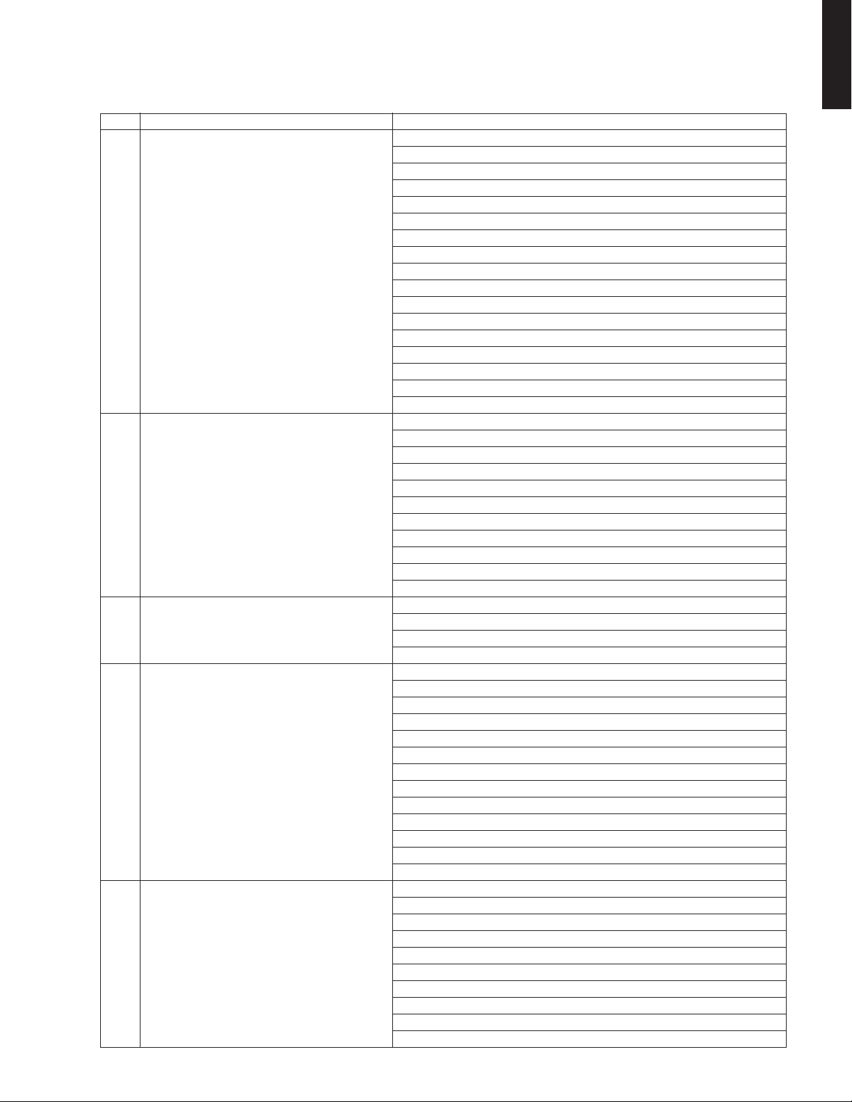
■ SELF DIAGNOSIS FUNCTION (DIAG)/自己診断機能(ダイアグ)
This unit has self diagnosis functions that are intended for
inspection, measurement and location of faulty point.
There are 18 DIAG menu items, each of which has submenu items.
Listed in the table below are menu items and sub-menu
items.
Note that not all menu items listed will apply to the models
covered in this service manual.
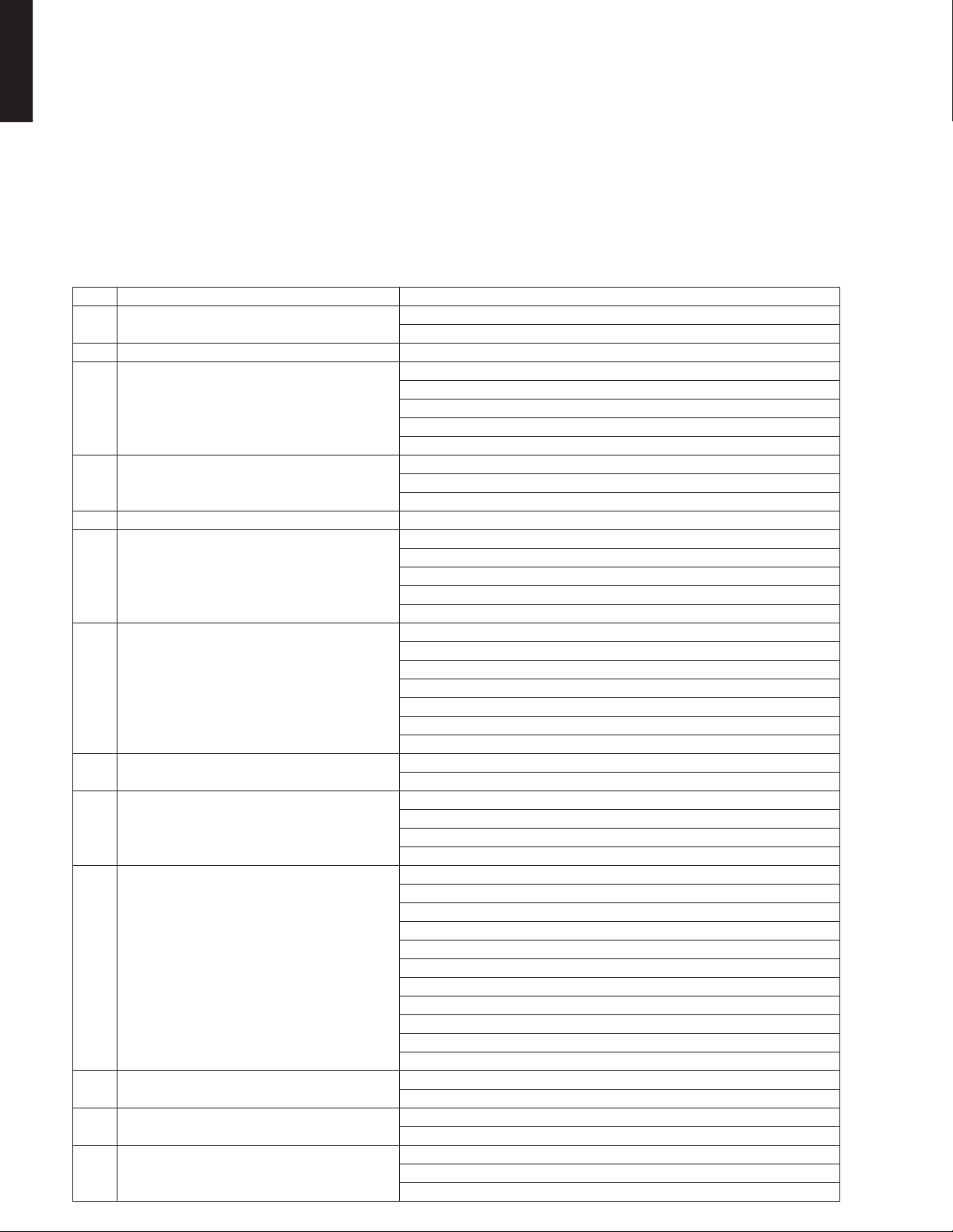
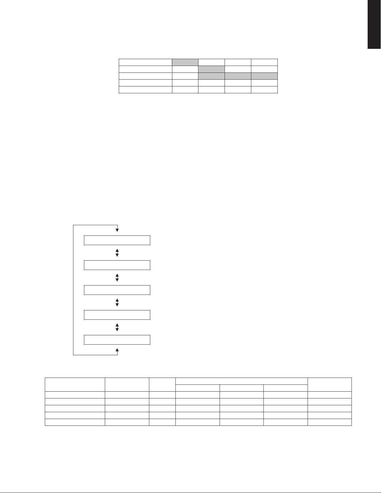
No. DIAG menu Sub-menu
1
2
3
4
5
6
7
8
9
10
11
12
13
18
BYPASS
AUDIO CHECK
SPEAKERS SET
6CH-INPUT
MIC CHECK
FL/OSD CHECK
TEST TONE
FACTORY PRESET
AD DATA CHECK
XM STATUS
(U, C models)
DOCK
USB
(Not applied to these models.)
DAB
(Not applied to these models.)
本機には、検査、測定、不良個所の発見を目的にした自己
診断機能(ダイアグ)があります。
ダイアグメニューは18個あり、そのそれぞれにサブメ
ニューがあります。
下表はダイアグメニュー一覧です。
下表の全ダイアグメニュー項目が、このサービスマニュア
ル記載のモデルに適用されるとは限りません。
ANALOG BYPASS
DSP BYPASS
AUDIO CHECK
FRNT : SML 0dB
CENTER : NONE
LFE/B : FRNT
TONE : MAX
TONE : MIN
6ch INPUT 6-ohm
6ch INPUT 8-ohm
LIM : , PLDET : , THM :
MIC CHECK
VFD CHECK
VFD DISP OFF
VFD DISP ALL
VFD DIMMER
CHECK PATTERN
TEST ALL
TEST FRNT L
TEST CENTER
TEST FRNT R
TEST SURR R
TEST SURR L
TEST LFE
PRESET INHI
PRESET RSRV
PD : , PV :
TH : , PL :
PI : , DE :
K0 : , K1 :
1k -1dB/44
1k -61dB/44
Mute/44
XM Tone/44
ISO Tone/44
1k -1dB/32
1k -61dB/32
Mute/32
XM Tone/32
ISO Tone/32
Bus Power : OFF
DOCK :
DOCK ignore
USB 1
USB 2
DAB 1
DAB 2
DAB 3
Page 6
RX-V461/HTR-6040/DSP-AX461
No. DIAG menu Sub-menu
14
IF STATUS
(Not applied to these models.)
IF 1
IF 2
IF 3
IF 4
IF 5
IF 6
IF 7
IF 8
IF 9
IF 10
IF 11
IF 12
IF 13
IF 14
IF 15
IF 16
IF 17
15
PROTECTION
PRD L :
PRD H :
PRV L :
PRV H :
THM :
PLD8H :
PLD8L :
PLD6H :
PLD6L :
PRI :
PDET :
16
PROTECTION HISTORY
History 1
History 2
History 3
History 4
17
SOFT SWITCH
SW MODE
MODEL
DESTINATION
TUNER DESTINATION
VIDEO FORMAT
AAC
OSD
YPAO
RDS
XM
DAB
USB
DOCK (iPod)
18
ROM VER/SUM
VERSION
ALL CHECKSUM
PROGRAM CHECKSUM
SPI CHECKSUM
SPD CHECKSUM
XM VERSION
DAB VERSION
FlashROM TEST
SDRAM TEST
EEPROM TEST
RX-V461/HTR-6040/
DSP-AX461
19
Page 7

RX-V461/HTR-6040/DSP-AX461
DSP-AX461
• Starting DIAG
RX-V461/HTR-6040/
Press the “STANDBY/ON” key while simultaneously
pressing those two keys of the main unit as indicated
in the figure below.
• Starting DIAG in the protection cancel mode
If the protection function works and causes hindrance
to trouble diagnosis, cancel the protection function as
described below, and it will be possible to enter the
DIAG mode. (The protection functions other than the
excess current detect function will be disabled.)
Press the “STANDBY/ON” key while simultaneously
pressing those two keys indicated in the figure above.
At this time, keep pressing those two keys for 3 seconds or longer.
In this mode, the [SLEEP] segment of the FL display
of the main unit flashes to indicate that the mode is
DIAG mode with the protection functions disabled.
● ダイアグの起動
本体の下図に示すキーを同時に押しながらSTANDBY/
ONキーを押すと、ダイアグが起動します。
Keys of main unit / 本機キー
Turn on the power while pressing these keys. /
これらのキーを同時に押しながら、電源オンする。
● プロテクション解除モードでの起動
プロテクションが動作することにより、故障箇所の診
断に支障をきたすような場合は、次の方法によりプロ
テクションを解除した状態でダイアグモードに入るこ
とができます。(過電流検出以外のプロテクション動
作を解除する)
上図のキーを同時に押しながらSTANDBY/ONキー
を押します。このとき、上図のキーを3秒以上押し続
けてください。
このモードでは本体FLの「SLEEP」セグメントが点滅
し、プロテクションを解除した状態でのダイアグモー
ドであることを知らせます。
CAUTION!
Using this product with the protection function disabled may cause damage to the main unit. Use special care for this point when using this mode.
• Canceling DIAG
1. Before canceling DIAG, execute setting for FACTORY PRESET of DIAG menu No.8 (Memory initialization inhibited or Memory initialized).
* In order to keep the user memory stored, be
sure to select PRESET INHIBITED (Memory initialization inhibited).
2. Turn off the power by pressing the “STANDBY/ON”
key of the main unit.
• Display provided when DIAG started
On the FL display of the main unit, an opening message (including the protection history) appears for a
few seconds followed by the DIAG menu display (1.
ANALOG BYPASS).
注意!
プロテクション解除モードでの起動は、危険な状態でも
プロテクションが作動しないため、動作させると本機を
破壊することがあります。
このモードを使用する場合は十分注意してください。
● ダイアグの解除
1. ダイアグを解除する前に、ダイアグメニューNo.8
FACTORYPRESET(メモリーの初期化禁止/また
はメモリーの初期化)の設定をします。
※ ユーザーメモリーを保持したい場合は、必ず
PRESETINHIBITED(メモリー初期化禁止)を選
択してください。
2. 本機のSTANDBY/ONキーを押し、電源オフしま
す。
● ダイアグ起動時の表示
本機のFLディスプレイには、オープニング(プロテク
ション履歴)が表示され、数秒後にダイアグメニュー
表示(1.ANALOGBYPASS)となります。
20
Page 8
RX-V461/HTR-6040/DSP-AX461
When there is no history of protection function: プロテクション履歴が無い場合:
Opening message / オープニング表示
When there is no protection history
プロテクション履歴が無い場合
After a few seconds / 数秒後
DIAG menu display / ダイアグメニュー表示
RX-V461/HTR-6040/
DSP-AX461
NO PROTECTION
When there is a history of protection function:
When there is a history of protection function due
to excess current
PRI PRT:xxx
Cause: An excessive current flowed through the
power amplifier.
Supplementary information:
As current of the power amplifier is detected,
the abnormal channel can be identified by
checking the current detect transistor.
Turning on the power without correcting the
abnormality will cause the protection function to work immediately and the power supply will instantly be shut off.
Note)
• Applying the power to the main unit without correcting the abnormality can be dangerous and
cause additional circuit damage. To avoid this, if
“PRI” and “PRD” protection function has been activated 3 times continuously, the power will not
turn on even when the “STANDBY/ON’ key is
pressed. In order to turn on the power again, disconnect the power cable of the main unit from the
AC outlet once and then reconnect it again.
• The output transistors in each amplifier channel
should be checked for damage before applying
power of the main unit.
• Amplifier current should be monitored by measuring across the emitter resistors for each channel.
1.ANLOG BYPASS
プロテクション履歴がある場合:
過電流によるプロテクション履歴がある場合
AD value when the protection function is working
プロテクション動作時のA/D値
原因: パワーアンプに過電流が流れた。
補足: パワーアンプの電流を検出していますので、
電流検出トランジスタをチェックすれば異常
チャンネルが特定できます。
異常状態のまま電源オンすると、瞬時にプロ
テクションがかかり、すぐに電源が切れま
す。
注意!
・ 異常状態のまま本機の電源を入れると、危険な状態に
なり、さらに回路が損傷を受ける原因になります。そ
のため連続してPRIおよびPRDプロテクションが
働いた場合、3回目からSTANDBY/ONキーを押して
も電源が入らなくなります。再度電源を入れる場合、
一度本機の電源コードをAC電源コンセントから抜いて
接続し直してください。
・ 本機の電源をいれる前に、各アンプのチャンネル内の
出力トランジスタに損傷がないかチェックしてくださ
い。
・ アンプの電流は、各チャンネルのエミッターの抵抗器
間で測定することによりモニターしてください。
to abnormal DC output
PRD PRT:xxx
Cause: DC output of the power amplifier is abnormal.
Supplementary information:
The protection function worked due to a DC
voltage appearing at the speaker terminal.
A cause could be a defect in the amplifier.
If the power is turned on with the abnormality
unsolved, the protection function works in
about 3 seconds to turn off the power.
DC出力異常によるプロテクション履歴がある場合When there is a history of protection function due
AD value when the protection function is working
プロテクション動作時のA/D値
原因: パワーアンプのDC出力が異常。
補足: アンプの故障でスピーカー端子に直流電圧が
掛かるなどが原因で、プロテクションが働い
たことを示します。
異常状態のままパワーオンすると、約3秒後
にプロテクションが掛かり、電源が切れま
す。
21
Page 9

RX-V461/HTR-6040/DSP-AX461
DSP-AX461
RX-V461/HTR-6040/
to abnormal voltage in the power supply section
Cause: The voltage in the power supply section is
Supplementary information:
When there is a history of protection function due
to excessive heat sink temperature
Cause: The temperature of the heat sink is excessive.
Supplementary information:
PRV PRT:xxx
abnormal.
The protection function worked due to a defect or overload in the power supply.
If the power is turned on with the abnormality
unsolved, the protection function works in
about 1 second to turn off the power.
THM PRT:xxx
The protection function worked due to the
temperature limit being exceeded.
Causes could be poor ventilation or a defect
related to the thermal sensor.
電源部の電圧異常によるプロテクション履歴がある場合When there is a history of protection function due
AD value when the protection function is working
プロテクション動作時のA/D値
原因: 電源部の電圧が異常。
補足: 電源電圧による原因で、プロテクションが働
いたことを示します。
異常状態のままパワーオンすると、約1秒後
にプロテクションが掛かり、電源が切れま
す。
ヒートシンクの異常温度によるプロテクション履歴が
ある場合
AD value when the protection function is working
プロテクション動作時のA/D値
原因: ヒートシンクの温度が異常。
補足: 温度制限を越えた原因で、プロテクションが
働いたことを示します。
If the power is turned on with the abnormality unsolved,
the protection function works in about 1 second to turn off
the power.
For detection of each protection function, refer to DIAG
menu described later.
History of protection function
When the protection function has worked, its history
is stored in memory with a backup.
Even if no abnormality is noted while servicing the
unit, an abnormality which has occurred previously
can be defined as long as the backup data has been
stored.
The history of the protection function is cleared
when DIAG is cancelled by selecting PRESET RESERVED (Memory initialized) of DIAG menu No. 8 or
when the backup data is erased.
異常状態のままパワーオンすると、約1秒後にプロテ
クションが掛かり、電源が切れます。
各プロクテクションの検出に関しては、後述のダイア
グメニューを参照してください。
プロテクションの履歴
プロテクションが働いた場合、履歴をバックアップして
記憶しています。
サービスのときに異常が認められなくても、バックアッ
プが残っていれば、お客様のところで起きた異常を区別
できます。
ダイアグメニューNo.8PRESETRESERVED(メモリー
の初期化)を選んでダイアグを解除した場合または、バッ
クアップが消えた場合にプロテクションの履歴はクリア
されます。
22
Page 10
RX-V461/HTR-6040/DSP-AX461
RX-V461/HTR-6040/
DSP-AX461
• Operation procedure of DIAG menu and
Sub-menu
There are 18 menu items, each of having sub-menu
items.
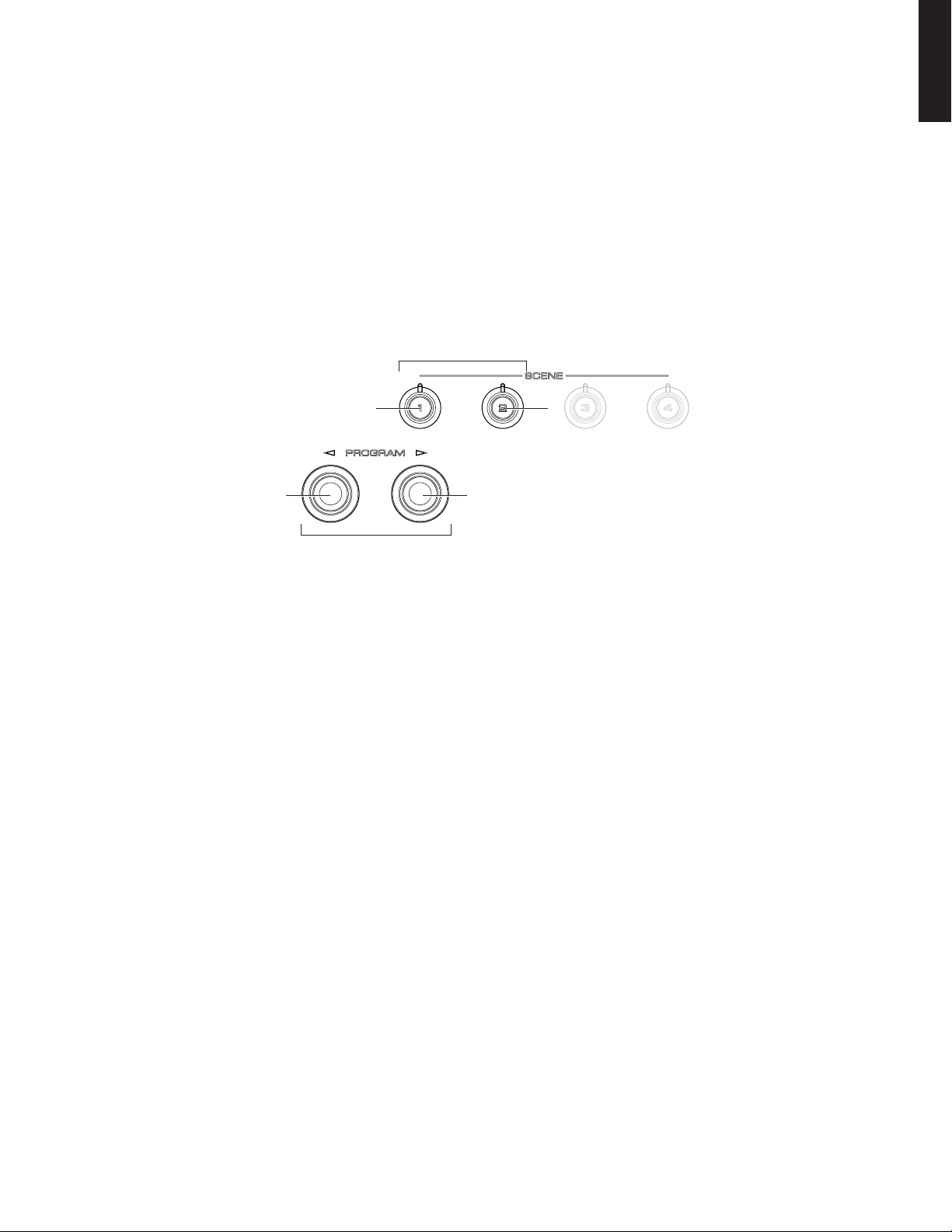
DIAG menu selection:
Select the menu using “>” (forward) and “<” (reverse)
keys of PROGRAM.
Sub-menu selection:
Select the sub-menu using “SCENE 2” (forward) and
“SCENE 1” (Reverse) keys.
Keys of main unit / 本機キー
Sub-menu selection
サブメニューの選択
Reverse
逆送り
Reverse
逆送り
● ダイアグメニューとサブメニューの操作
ダイアグにはNo.1〜18のメニューがあり、そのそれ
ぞれにサブメニューがあります。
ダイアグメニューの選択:
PROGRAM>(順送り)、PROGRAM<(逆送り)
キーで選択します。
サブメニューの選択:
SCENE2(順送り)、SCENE1(逆送り)キーで選
択します。
Forward
順送り
Forward
順送り
DIAG menu selection
ダイアグメニューの選択
• Functions in DIAG mode
In addition to the DIAG menu items, functions as listed
below are available.
• Power on/off
• Master volume
• Muting
• Speakers A/B/OFF
• Input selection
• Audio select
• Tone control
* Functions related to the tuner and the set menu are
not available.
• Initial settings used to start DIAG
The following initial settings are used when starting
DIAG.
When DIAG is canceled, these settings are restored
to those before starting DIAG.
• Master volume: -20 dB
• Input: DVD (MULTI CHANNEL INPUT OFF)
• Effect level: 0 dB
• DIAG menu: 1. ANALOG BYPASS
● ダイアグ中の機能
ダイアグメニューの他に、以下の機能が動作します。
・ パワーオン/オフ
・ マスターボリューム
・ ミューティング
・ スピーカーA/B/OFF
・ インプット切り換え
・ オーディオセレクト
・ トーンコントロール
※ チューナー関連、セットメニュー関連は機能しませ
ん。
●ダイアグ開始時の初期設定
ダイアグ開始時に以下のような設定になります。
ダイアグ解除時にはダイアグ開始前の状態に戻りま
す。
・ マスターボリューム:-20dB
・ インプット:DVD(マルチチャンネルインプットオフ)
・ エフェクトレベル:0dB
・ ダイアグメニュー:1.ANALOGBYPASS
23
Page 11
RX-V461/HTR-6040/DSP-AX461
DSP-AX461
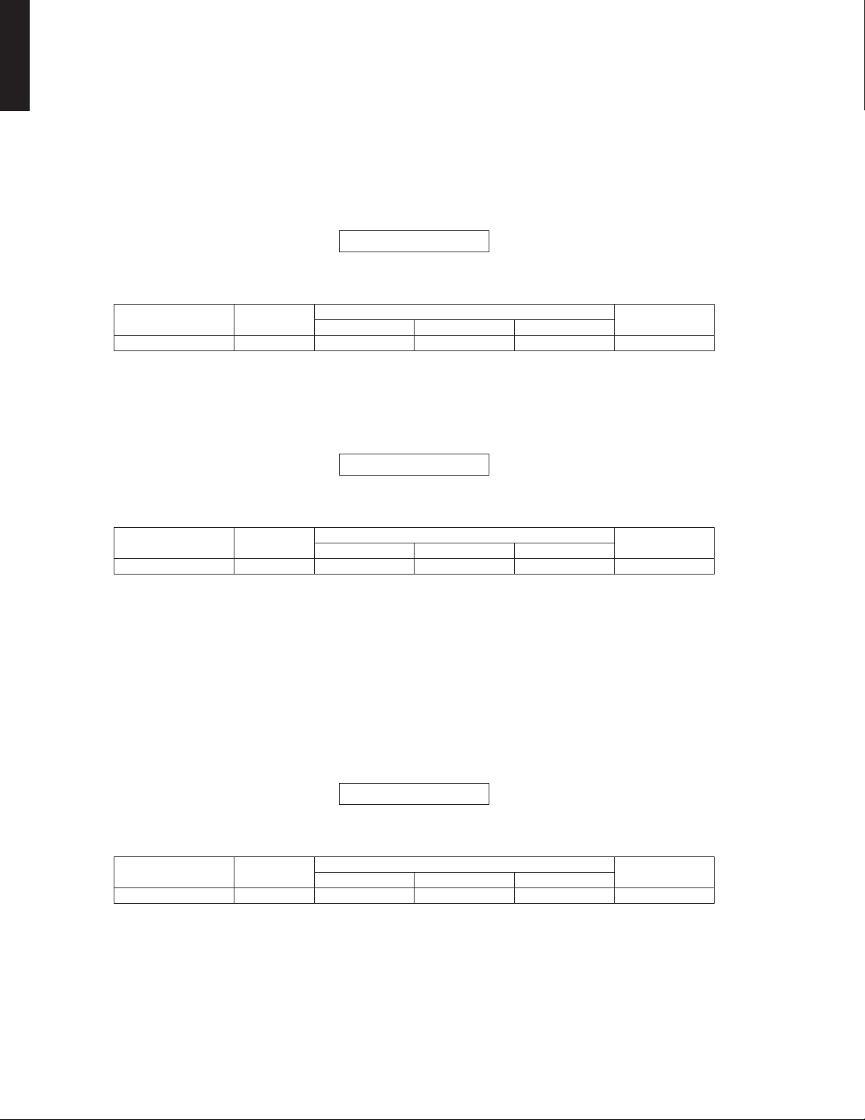
• Details of DIAG menu
RX-V461/HTR-6040/
1. BYPASS
Using the sub-menu, it is possible to select ANALOG
BYPASS output or DSP BYPASS output.
ANALOG BYPASS
The analog input sound signal is output to FRONT L/R
with EFFECT OFF.
DSP BYPASS
The digital input sound signal is output to FRONT L/R
with EFFECT OFF.
1.ANLOG BYPASS
INPUT: DVD ANALOG
SPEAKER OUT: 1 kHz, SUBWOOFER OUTPUT: 50 Hz
Input level Volume
Both ch, -20 dBm +6.0 dB
FRONT
+11.5 dBm
1.DSP BYPASS
● ダイアグメニュー詳細
1. BYPASS
サブメニューによりANALOGBYPASS/DSPBYPASS
が選択可能です。
ANALOGBYPASS
アナログ入力の音声信号をEFFECTOFFでFRONTL/
Rへ出力します。
SPEAKER OUT SUBWOOFER
CENTER
-∞
SURROUND
-∞ -∞
DSPBYPASS
デジタル入力の音声信号をEFFECTOFFでFRONTL/
Rへ出力します。
OUTPUT
INPUT: DVD ANALOG
SPEAKER OUT: 1 kHz, SUBWOOFER OUTPUT: 50 Hz
Input level Volume
Both ch, -20 dBm +6.0 dB
FRONT
+11.5 dBm
2. AUDIO CHECK
The input sound signal is output.
* When the inputted sound signal is 2 ch L/R, it is
distributed as follows when output.
L ch: FRONT L, CENTER, SURROUND L,
LFE ( L ch +10 dB)
R ch: SURROUND R
2.AUDIO CHECK
INPUT: DVD ANALOG
SPEAKER OUT: 1 kHz, SUBWOOFER OUTPUT: 50 Hz
Input level Volume
Both ch, -20 dBm +6.0 dB
FRONT
+11.5 dBm
SPEAKER OUT SUBWOOFER
CENTER
-∞
SURROUND
-∞ -∞
OUTPUT
2. AUDIOCHECK
入力された音声信号を出力します。
※ 入力された音声信号が2chL/Rの場合は、下記のよ
うに振り分け出力します。
Lch: FRONTL、CENTER、SURROUNDL、
LFE(Lch+10dB)
Rch: SURROUNDR
SPEAKER OUT SUBWOOFER
CENTER
+11.5 dBm
SURROUND
+11.5 dBm 0 dBm
OUTPUT
24
Page 12
RX-V461/HTR-6040/DSP-AX461
RX-V461/HTR-6040/
DSP-AX461
3. SPEAKER SET
The analog switch settings for each sub-menu are as
shown in the table below.
FRONT : SML 0dB
CENTER : NONE
LFE/B : FRNT
TONE : MAX
TONE : MIN
LARGE: This mode is used for a speaker with high
bass reproduction performance (a large unit).
Full bandwidth signals are output.
SMALL: This mode is used for a speaker with low bass
reproduction performance (a small unit).
The signals of 90 Hz or less are mixed into
the channel specified by LFE/BASS.
NONE: This mode is used for no center speaker.
The center content is reduced by 3 dB and
distributed to FRONT L/R.
SWFR: LFE of 5.1 ch signal or LFE/BASS lower than
90 Hz is output through SUBWOOFER OUT.
FRONT: LFE of 5.1 ch signal or LFE/BASS lower
than 90 Hz is distributed to FRONT L/R.
SMALL
LARGE
LARGE
LARGE
LARGE
3. SPEAKERSET
各サブメニューにおけるアナログスイッチの設定は以
下の通りです。
LARGE
NONE
SMALL
LARGE
LARGE
LARGE
LARGE
SMALL
LARGE
LARGE
SWFR
SWFR
FRONT
SWFR
SWFR
LARGE: 低音再生能力の高い(ユニットの大きい)ス
ピーカーを使用するモードです。
全帯域が出力されます。
SMALL: 低音再生能力の低い(ユニットの小さい)ス
ピーカーを使用するモードです。
90Hz以下がLFE/BASSで指定したチャンネ
ルにミックスされます。
NONE: センタースピーカーを使用しないモードです。
センター成分は-3dBされて、FRONTL/Rに
振り分けられます。
SWFR: 5.1ch信号のLFEまたは90Hz以下のLFE/BASS
がSUBWOOFEROUTに出力されます。
FRONT: 5.1ch信号のLFEまたは90Hz以下のLFE/
BASSをFRONTL/Rに振り分けます。
3.FRNT:SML 0dB
3.CENTER NONE
3.LFE/B:FRNT
3.TONE:MAX
3.TONE:MIN
INPUT: DVD ANALOG
SPEAKER OUT: 1 kHz, SUBWOOFER OUTPUT: 50 Hz
Sub-menu
FRONT : SML 0dB
CENTER : NONE
LFE/B : FRNT
TONE : MAX
TONE : MIN
Input level Volume
Both ch, -20 dBm
Both ch, -20 dBm
Both ch, -20 dBm
Both ch, -20 dBm
Both ch, -20 dBm
FRONT: SML 0dB
The FRONT L/R signal, when 90 Hz or lower, is mixed to the channel specified by LFE/BASS.
FRONTL/Rの信号の90Hz以下がLFE/BASSで指定したチャンネルにミックスされます。
CENTER: NONE
The CENTER signal is distributed to FRONT L/R.
CENTERの信号をFRONTL/Rに振り分けます。
LFE / BASS: FRONT
The LFE (SUBWOOFER) signal is distributed to FRONT L/R.
LFE(SUBWOOFER)の信号をFRONTL/Rに振り分けます。
TONE: MAX
The signal is output with the tone control [BASS +10 dB, TREBLE + 10 dB].
トーンコントロール[BASS+10dB、TREBLE+10dB]で出力します。
TONE: MIN
The signal is output with the tone control [BASS -10 dB, TREBLE - 10 dB].
トーンコントロール[BASS-10dB、TREBLE-10dB]で出力します。
+6.0 dB
+6.0 dB
+6.0 dB
+6.0 dB
+6.0 dB
FRONT
+11.5 dBm
+11.5 dBm
+11.5 dBm
+14.5 dBm
+8.5 dBm
SPEAKER OUT SUBWOOFER
CENTER
-∞
-∞
-∞
-∞
-∞
SURROUND
-∞
-∞
-∞
-∞
-∞
OUTPUT
-3.5 dBm
-∞
-∞
-∞
-∞
25
Page 13
RX-V461/HTR-6040/DSP-AX461
DSP-AX461
RX-V461/HTR-6040/
4. 6CH INPUT
The input source [MULTI CHANNEL INPUT] is selected.
It is possible to select the 6-ohm/8-ohm by using the
sub-menu.
6 ch INPUT 6-ohm
INPUT: MULTI CH INPUT
SPEAKER OUT: 1 kHz, SUBWOOFER OUTPUT: 50 Hz
6 ch INPUT 6-ohm
6 ch INPUT 8-ohm 6chINPUT8-ohm
INPUT: MULTI CH INPUT
SPEAKER OUT: 1 kHz, SUBWOOFER OUTPUT: 50 Hz
6 ch INPUT 8-ohm
Sub-menu
Sub-menu
Input level Volume
Both ch, -20 dBm +6.0 dB
Input level Volume
Both ch, -20 dBm +6.0 dB
4. 6CH INPUT
入力ソース[MULTICHANNELINPUT]が選択されま
す。
サブメニューにより、6オーム/8オームが選択可能で
す。
6chINPUT6-ohm
4.6ch INPUT 6 Ω
FRONT
+11.5 dBm
4.6ch INPUT 8 Ω
FRONT
+11.5 dBm
SPEAKER OUT SUBWOOFER
CENTER
+11.5 dBm
SPEAKER OUT SUBWOOFER
CENTER
+11.5 dBm
SURROUND
+11.5 dBm -3.5 dBm
SURROUND
+11.5 dBm -3.5 dBm
OUTPUT
OUTPUT
LIM/PLDET/THM
LIM: Setting value of LIM (Limiter control)
* As this is a development menu, do not
change the setting value.
PLDET: Power limiter detection
The A/D conversion value during operation
is displayed.
THM: Thermo protection detection
The A/D conversion value during operation
is displayed.
(Reference voltage: 3.3 V=255)
4.255:255: 83
5. MIC CHECK
The signals input through the microphone are output
of FRONT L/R via A/D and D/A.
LIM/PLDET/THM
LIM: LIM(リミッター制御)の設定値
※ 開発用メニューのため、設定値の変更は行
わないでください。
PLDET: パワーリミッターの検出
動作時のA/D変換値が表示されます。
THM: 温度プロテクションの検出
動作時のA/D変換値が表示されます。
(基準電圧:3.3V=255)
THM (Thermo protection detection / 温度プロテク
ションの検出)
PLDET (Power limiter detection / パワーリミッターの
検出)
LIM (Limiter control / リミッター制御)
5.MICCHECK
マイク入力された信号をA/D−D/A経由でFRONTL/R
に出力します。
26
5.MIC CHECK
Page 14
RX-V461/HTR-6040/DSP-AX461
RX-V461/HTR-6040/
DSP-AX461
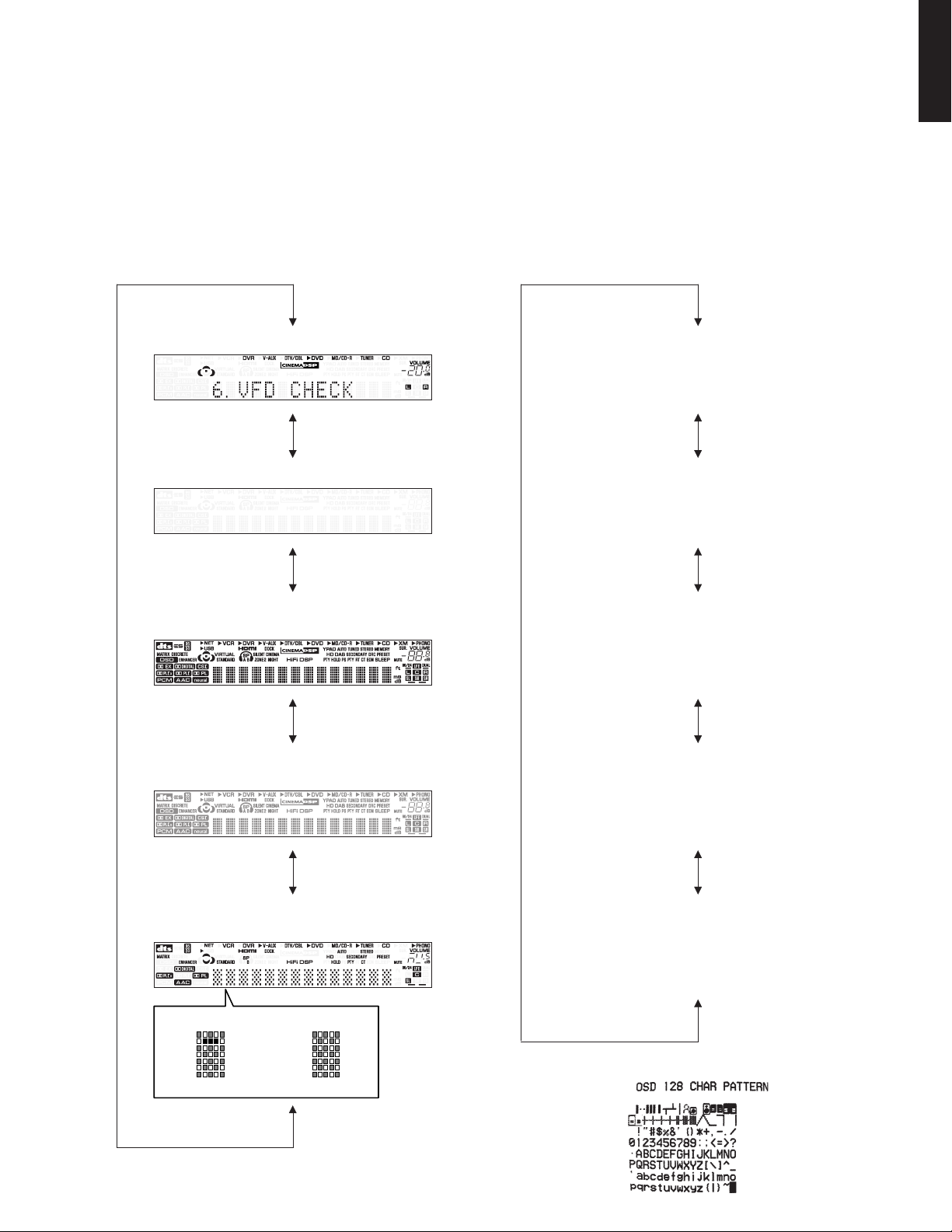
6. FL/OSD CHECK
Use this program to check the FL display section and
video control section. When checking the video control section, prepare a monitor, S video cable and
video pin cable and connect them.
Using the sub-menu operation, selection items of the
FL display section and video display section vary as
shown below.
For audio signal processing, use STRAIGHT.
Checking FL display section /
FL表示部のチェック
Initial display / 初期表示
All segments OFF / 全セグメント消灯
6. FL/OSDCHECK
FL表示部および映像表示部のチェックプログラムで
す。映像制御部をチェックする場合には、モニター、
Sビデオケーブル、ビデオ用ピンケーブルを準備し接
続します。
サブメニュー操作により、FL表示部と映像表示部の選
択が以下のように連動して変わります。
オーディオ信号処理はSTRAIGHTです。
Check of the Video control section. (Monitor out) /
映像表示部のチェック(モニター出力)
Initial display (OSD OFF) /
初期表示(OSD表示オフ)
OSD OFF /
OSD表示オフ
All segments ON (dimmer 100 %) /
全セグメント点灯(ディマー100%)
All segments ON (dimmer 50 %) /
全セグメント点灯(ディマー50%)
Lighting of segments in lattice /
セグメント格子状点灯
Lighting in lattice / 格子状点灯
Normal / 正常Short / ショート
OSD OFF /
OSD表示オフ
OSD characters ON /
OSDキャラクター表示オン
OSD characters ON /
OSDキャラクター表示オン
OSD characters / OSDキャラクター表示
27
Page 15
RX-V461/HTR-6040/DSP-AX461
DSP-AX461
RX-V461/HTR-6040/
7. TEST TONE
The noise generator with a built-in microprocessor
outputs the noise through the channels specified by
the submenu.
The noise frequency for LFE (SUBWOOFER) is 35 to
80 Hz.
Other than that, the noise frequency is 500 to 2 kHz.
7.TEST ALL
7.TEST FRNT L
7.TEST CENTER
7.TEST FRNT R
7.TEST SURR R
7. TESTTONE
マイコンに内蔵されているノイズ発生回路によって、
サブメニューで指定したチャンネルへノイズを出力し
ます。
LFE(SUBWOOFER)用のノイズ周波数は35〜80Hz、
それ以外はノイズ周波数500〜2kHzとなります。
TEST ALL
Noise is output from all channels.
全チャンネルからノイズを出力。
TEST FRONT L
Noise is output from the FRONT L channel.
FRONTLチャンネルからノイズを出力。
TEST CENTER
Noise is output from the CENTER channel.
CENTERチャンネルからノイズを出力。
TEST FRONT R
Noise is output from the FRONT R channel.
FRONTRチャンネルからノイズを出力。
TEST SURROUND R
Noise is output from the SURROUND R channel.
SURROUNDRチャンネルからノイズを出力。
7.TEST SURR L
7.TEST LFE
TEST SURROUND L
Noise is output from the SURROUND L channel.
SURROUNDLチャンネルからノイズを出力。
TEST LFE (SUBWOOFER)
Noise is output from the LFE (SUBWOOFER) channel.
LFE(SUBWOOFER)チャンネルからノイズを出力。
8. FACTORY PRESET
This menu is used to reserve and inhibit initialization
of the back-up RAM.
The signals are processed using EFFECT OFF (The
L/R signal is output using ANALOG BYPASS).
8.PRESET INHI
8.PRESET RSRV
PRESET INHIBIT (Initialization inhibited) / PRESETINHIBIT(初期化禁止)
Back-up RAM initialization is not executed. Select this sub-menu to protect the values set by the user.
バックアップ用RAMの初期化は行われません。ユーザーの設定値を保護するときは、こちらを選択し
てください。
PRESET RESERVED (Initialization reserved) / PRESETRESERVED(初期化予約)
Initialization of the back-up RAM is reserved. (Actually, initialization is executed the next time that the
power is turned on.)
Select this sub-menu to reset to the original factory settings or to reset the RAM.
Any protection history will be cleared.
バックアップ用RAMの初期化が予約されます。(実際に初期化されるのは、次回の電源投入時です。)
工場出荷時やバックアップ用RAMをリセットしたいときは、こちらを選択してください。
このとき、プロテクション履歴も初期化されます。
8. FACTORYPRESET
バックアップ用RAM(音場プログラムのパラメーター
やセットメニュー内容等)の初期化を予約/禁止しま
す。
信号処理はEFFECTOFF(ANALOGBYPASSでL/Rを
出力)です。
28
Page 16

RX-V461/HTR-6040/DSP-AX461
RX-V461/HTR-6040/
DSP-AX461
CAUTION: Before setting to the PRESET RESERVED,
write down the existing preset memory content of the tuner in a table as shown below.
(This is because setting to the PRESET
RESERVED will cause the user memory
content of the tuner to be erased.)
Preset Group P1 P2 P3 P4 P5 P6 P7 P8
A
B
C
D
E
9. A/D DATA CHECK
This menu is used to display the A/D conversion value
of the microprocessor which detects panel keys of the
main unit and protection functions in using the submenu.
When K0/K1 menu is selected, keys become non-operable due to detection of the values of all keys. However, it is possible to advance to the next sub-menu by
turning the VOLUME of the main unit. When using this
function, note that turning the VOLUME more than 1
click would cause the volume value to change.
During signal processing, the condition before execution is maintained.
* The figures in the diagram are given as reference
only.
注意: PRESETRESERVEDを選んで初期化を
する前に、チューナーのユーザーメモリー
内容を下表に書き写してください。
(初期化をすると、チューナーのユーザー
メモリーの内容は消えてしまいます。)
9. A/DDATACHECK
本機パネルキー、プロテクションなどを検出している
マイコンのA/D変換値を、サブメニューで表示しま
す。
K0/K1のメニューにすると、全キーの値を検出するた
めキー操作はできなくなりますが、本機のVOLUMEを
回すことにより、次のサブメニューに進めることがで
きます。このとき1クリック以上回すと、ボリューム
値が変化するので注意してください。
信号処理は実行前の状態を維持します。
※ 図中の数値は参考例です。
PD/PV
PD: PRD (Power amplifier DC protection detection)
The output of power amplifier DC (DC voltage)
is detected.
Normal value: 35 to 81 (Reference volt-
age: 3.3 V=255)
PV: PRV (Voltage protection detection)
Voltage detects: ACL, AC2, 10V, S9, +12,
-12, +5V and VP
Normal value: 84 to 153 (Reference volt-
age: 3.3 V=255)
* If PRD and PRV are out of the normal value range,
the protection function works to turn off the power.
PD: 57 PV:116
PD/PV
PD: PRD(パワーアンプDCプロテクションの検出)
パワーアンプDC(直流電圧)出力の検出。
正常値: 35〜81(基準電圧:3.3V=255)
PV: PRV(電圧プロテクションの検出)
検出電圧: ACL、AC2、10V、S9、+12、
-12、+5V、VP
正常値: 84〜153(基準電圧:3.3V=255)
※ PRDおよびPRVは正常値を外れるとプロテクショ
ンが働き、電源オフされます。
29
Page 17
RX-V461/HTR-6040/DSP-AX461
DSP-AX461
RX-V461/HTR-6040/
TH/PL
TH: THM (Thermo protection detection)
* If THM is out of the normal value range, the protec-
PL: PLDET (Power limiter detection)
U, C models (Reference voltage: 3.3 V=255)
LIM H: 255 / L: 102
(LIM: Limiter control)
R, K, A, L models (Reference voltage: 3.3V=255)
LIM H: 255 / L: 90
(LIM: Limiter control)
The temperature of the heat sink is detected.
Normal value: 0 to 124 (Reference volt-
age: 3.3 V=255)
tion function works to turn off the power.
The output voltage of power amplifier is
detected.
During normal operation
PLDET
During normal operation
PLDET
255
H
255
H
TH/PL
TH: THM(温度プロテクションの検出)
※ THMは正常値を外れるとプロテクションが働き、
電源オフされます。
PL: PLDET(パワーリミッターの検出)
TH: 83 PL:255
Value for starting limiter operation
77
L
Value for starting limiter operation
100
L
ヒートシンク温度の検出。
正常値:0〜124(基準電圧:3.3V=255)
パワーアンプ出力電圧の検出。
Value for canceling limiter operation
100
H
Value for canceling limiter operation
131
H
J model(基準電圧:3.3V=255)
通常値
PLDET
LIM H: 255 / L: 90
(LIM:リミッター制御)
255
H
PI/DE
PI: PRI (Current protection detection)
The current of the power amplifier is detected.
Normal value: 0 to 100 (Reference volt-
age: 3.3 V=255)
DE: PDET (Sub-trans power detection)
Normal value: 209 to 255 (Reference volt-
age: 3.3 V=255)
* If PRI and PDET are out of the normal value range,
the protection function works to turn off the power.
K0/K1
K0/K1: KEY0/KEY1 (Panel key of main unit)
A/D value of the key fails to function properly
when the standard value is deviated by ± 4.
In this case, check the constant of partial
pressure resistor, solder condition, etc.
Refer to table.
(Reference voltage: 3.3 V=255)
リミッター動作開始値
PI: 33 DE:255
リミッター動作解除値
100
L
131
H
PI/DE
PI: PRI(電流プロテクションの検出)
パワーアンプ電流の検出。
正常値: 0〜100(基準電圧:3.3V=255)
DE: PDET(サブトランス電源電圧の検出)
正常値: 209〜255(基準電圧:3.3V=255)
※ PRIおよびPDETは正常値を外れるとプロテクショ
ンが働き、電源オフされます。
K0/K1
K0/K1: KEY0/KEY1(本機パネルキー)
キーのA/D値は基準値から±4を外れると、
正常な動きをしません。
下表をご覧になり、各キーの分圧抵抗の定
数、ハンダ不良等の確認をしてください。
(基準電圧:3.3V=255)
30
K0:251 K1:252
Page 18

RX-V461/HTR-6040/DSP-AX461
RX-V461/HTR-6040/
DSP-AX461
Display / 表示
23 ± 4
42 ± 4
66 ± 4
92 ± 4
120 ± 4
147 ± 4
165 ± 4
182 ± 4
198 ± 4
217 ± 4
255
SCENE 1
SCENE 2
PROGRAM <
PROGRAM >
STRAIGHT
TONE CONTROL
SEARCH MODE
A/B/C/D/E
SPEAKERS
(KEY OFF)
The output check of XM radio antenna module is executed.
10.1k - 1dB/44
10.1k -61dB/44
1 kHz, -1 dB / 44.1 kHz
The test tone (1 kHz, -1 dB / 44.1 kHz) is output.
1 kHz, -61 dB / 44.1 kHz
The test tone (1 kHz, -61 dB / 44.1 kHz) is output.
KEY0
FM/AM
KEY1
SCENE 3
SCENE 4
DIRECT
AUDIO SELECT
INPUT <
INPUT >
PRESET/TUNING <
PRESET/TUNING >
MEMORY
TUNING
(KEY OFF)
10. XMSTATUS(U、Cmodels)10. XM STATUS (U, C models)
10.MUTE /44
10.XM TONE /44
10.ISO TONE/44
10.1k - 1dB/32
10.1k -61dB/32
10.MUTE /32
10.XM TONE /32
10.ISO TONE/32
Mute / 44.1 kHz
No signal is output.
XM tone / 44.1 kHz
The XM tone / 44.1 kHz is output.
ISO tone / 44.1 kHz
The ISO tone /44.1 kHz is output.
1 kHz, -1 dB / 32.0 kHz
The test tone (1 kHz, -1 dB / 32.0 kHz) is output.
1 kHz, -61 dB / 32.0 kHz
The test tone (1 kHz, -61 dB / 32.0 kHz) is output.
Mute / 32.0 kHz
No signal is output.
XM tone / 32.0 kHz
The XM tone / 32.0 kHz is output.
ISO tone / 32.0 kHz
The ISO tone / 32.0 kHz is output.
10.BUS PWR:OFF
XM bus power: OFF
The power of XM module is turned off.
31
Page 19

RX-V461/HTR-6040/DSP-AX461
DSP-AX461
RX-V461/HTR-6040/
11. DOCK
This menu is used to test the DOCK connector without
the iPod itself.
After turning off the power, short between pins No. 14
(TX) and No. 18 (RX), between pins No. 1 (PWR) and
No. 17 (ACCPOW) and between pins No. 4 (iPDET)
and No. 8 (DGND).
Start the DIAG function and select the menu.
The check result is displayed according to the following display specifications.
original state.
15 16 17 18
9 10 1112 1314
3 4 56 78
1 2
19
DOCK
20 21
11. DOCK
iPod本体無しで、DOCKコネクタの検査を行うメ
ニューです。
電源オフの状態にしてから、DOCKコネクタの14ピン
(TX)と18ピン(R X)、1ピン(PWR)と17ピン
(ACCPOW)、4ピン(iPDET)と8ピン(DGND)を
ショートさせます。
ダイグを起動してメニューを選択します。
下記表示仕様に従って、チェック結果が表示されま
す。
注) ショート箇所は、必ず元に戻してください。Note) Be sure to return the shorted locations to their
11.DOCK:NG NNN
All Y / すべてY = “OK”
Others / その他 = “NG”
Check item / チェック項目 Result / 結果 Display / 表示
UART loop back test /
UARTループバックテスト
iPAP (iPod accessory power) detection /
iPAP(iPodaccessorypower)検出
iPDET (iPod installation to DOCK) detection /
iPDET(iPodinstallationtoDOCK)検出
DOCK ignore
When DOCK and iPod are connected, the input
source [DOCK (iPod)] is made invalid and [V-AUX] is
selected.
11.DOCK IGNORE
12. USB CHECK
Not applied to these models.
12.USB 1 12.USB 2
OK
NG
IC402 pin No. 1
IC402 pin No. 12
DOCK無効
DOCKおよびiPodを接続している時、入力ソース
[DOCK(iPod)]を無効にして[V-AUX]に切り替えま
す。
12. USBCHECK
このモデルには適用されません。
High
Low
Low
High
Y
N
Y
N
Y
N
32
13. DAB CHECK
Not applied to these models.
13.DAB 1 13.DAB 3
13. DABCHECK
このモデルには適用されません。
• • • • • • •
Page 20

RX-V461/HTR-6040/DSP-AX461
RX-V461/HTR-6040/
DSP-AX461
14. IF STATUS (Input function status)
Not applied to these models.
14.IF 1 14.IF 17
15. PROTECTION SETTING
The A/D setting value of each protection is displayed.
(Reference voltage: 3.3 V=255)
15.PRD L : 35
15.PRD H : 81
15.PRV L : 83
15.PRV H : 153
PRD (Amplifier DC protection) Low
The minimum preset value of PRD is displayed.
PRDの下限設定値が表示されます。
PRD (Amplifier DC protection) High
The maximum preset value of PRD is displayed.
PRDの上限設定値が表示されます。
PRV (Voltage protection) Low
The minimum preset value of PRV is displayed.
PRVの下限設定値が表示されます。
PRV (Voltage protection) High
The maximum preset value of PRV is displayed.
PRVの上限設定値が表示されます。
14.IFSTATUS
このモデルには適用されません。
• • • • • • •
15. PROTECTIONSETTING
各プロテクションのA/D設定値が表示されます。(基準
電圧:3.3V=255)
15.THM : 124
15.PLD8 H: 100
15.PLD8 L: 131
15.PLD6 H: 100
15.PLD6 L: 131
15.PRI 100
15.PDET 209
THM (Thermo protection) High
The maximum preset value of THM is displayed.
THMの上限設定値が表示されます。
PLD (PLDET (Power limiter detection)) 8-ohm Low
The value for starting limiter operation of PLD8 is displayed.
PLD8のリミッター動作開始値が表示されます。
PLD (PLDET (Power limiter detection)) 8-ohm High
The value for canceling limiter operation of PLD8 is displayed.
PLD8のリミッター動作解除値が表示されます。
PLD (PLDET (Power limiter detection)) 6-ohm Low
The value for starting limiter operation of PLD6 is displayed.
PLD6のリミッター動作開始値が表示されます。
PLD (PLDET (Power limiter detection)) 6-ohm High
The value for canceling limiter operation of PLD6 is displayed.
PLD6のリミッター動作解除値が表示されます。
PRI (Amplifier current protection) High
The maximum preset value of PRI is displayed.
PRIの上限設定値が表示されます。
PDET Low
The minimum preset value of PDET is displayed.
PDETの下限設定値が表示されます。
33
Page 21

RX-V461/HTR-6040/DSP-AX461
DSP-AX461
RX-V461/HTR-6040/
16. PROTECTION HISTORY
Four protection histories are displayed.
Example / 例
16.PRI: 90
Example / 例
16.PRD: 34
Example / 例
16.THM: 60
Example / 例
16.NO PROT
16. PROTECTIONHISTORY
過去のプロテクション履歴が4つまで表示されます。
History 1 / 履歴1
History 2 / 履歴2
History 3 / 履歴3
History 4 / 履歴4
34
Page 22

RX-V461/HTR-6040/
RX-V461/HTR-6040/DSP-AX461
DSP-AX461
17. SOFTSWITCH17. SOFT SWITCH
Note) As this is a development menu, do not change
the function setting.
Changing the function setting may hinder the
proper operation.
This menu is used to switch the function settings on
P.C.B. through the software to activate the main unit.
The protection function follows the P.C.B. settings.
* As this is a development menu, it is not possible to
describe the details.
17.MODE:PCB
17.MODEL:461
17.DEST : UC
17.TUNER: UC
注) 開発用メニューのため、機能設定の変更は行わな
いでください。
機能設定を変更した場合、正常に動作しないこと
があります。
P.C.B.上の機能設定をソフト的に切り替えて、本機を
動作させる機能です。
プロテクション機能は、P.C.B.の設定に従います。
※ 開発用メニューのため、詳細に関しては記載できま
せん。
Switch mode
Model
Destination
Tuner destination
17.VIDEO:NTSC
17.AAC : NOT
17.OSD :AVAIL
17.YPAO: NOT
17.RDS : NOT
17.XM : NOT
17.DAB : NOT
17.USB : NOT
VIDEO format
AAC
OSD
YPAO
RDS
XM
DAB
USB
17.DOCK:AVAIL
DOCK (iPod)
35
Page 23

RX-V461/HTR-6040/DSP-AX461
DSP-AX461
RX-V461/HTR-6040/
18. ROM VER/SUM
The version and checksum are displayed. The signal
is processed using EFFECT OFF.
The checksum is obtained by adding the data at every
8-bit for each program area and expressing the result
as a 4-figure hexadecimal data.
18. VER. H045
18.A.SUM: F25D
18.P.SUM: 8D14
18. ROMVER/SUM
プログラムのバージョン、チェックサムを表示しま
す。信号はエフェクトオフです。
チェックサムは、プログラムエリア別にデータを8
ビットごとに加算していき、4桁の16進データで現し
たものです。
Version
Firmware version of microprocessor (IC101 DSP P.C.B.) is displayed.
マイコン(IC101DSPP.C.B.)のファームウェアのバージョンを表示します。
All checksum
Checksum value of microprocessor (IC101 DSP P.C.B.) is displayed.
マイコン(IC101DSPP.C.B.)のチェックサム値を表示します。
Program checksum
Checksum value of application and standby code program is displayed.
アプリケーションおよびスタンバイコードプログラムのチェックサム値を表示します。
18.SPI.S: E598
18.SPD.S: CD02
18. XM : XM09
18.DAB:
FROM TEST:
SPI (Serial Peripheral Interface) checksum
Checksum value of SPI firmware update code is displayed.
SPIファームウェアアップデートコードのチェックサム値を表示します。
SPD (S/PDIF) checksum
Checksum value of SPD firmware update code is displayed.
SPDファームウェアアップデートコードのチェックサム値を表示します。
XM version
Firmware version of XM is displayed.
XMのファームウェアのバージョンを表示します。
DAB version
Firmware version of DAB is displayed. (Not applied to these models.)
DABのファームウェアのバージョンを表示します。(このモデルには適用されません。)
FlashROM test
The read/write test of microprocessor (IC101 DSP P.C.B.) and flash ROM (IC201 DSP P.C.B.).
マイコン(IC101DSPP.C.B.)とフラッシュROM(IC201DSPP.C.B.)の読み出し/書き込みテス
トを行います。
NoEr: No error detected / 不良検出なし NG: An error is detected / 不良検出あり
36
DRAM TEST:
PROM TEST:
SDRAM test
The read/write test of microprocessor (IC101 DSP P.C.B.) and SDRAM (IC202 DSP P.C.B.).
マイコン(IC101DSPP.C.B.)とSDRAM(IC202DSPP.C.B.)の読み出し/書き込みテストを行い
ます。
NoEr: No error detected / 不良検出なし NG: An error is detected / 不良検出あり
EEPROM test
The read/write test of microprocessor (IC101 DSP P.C.B.) and EEPROM (IC102 DSP P.C.B.).
マイコン(IC101DSPP.C.B.)とEEPROM(IC102DSPP.C.B.)の読み出し/書き込みテストを行
います。
NoEr: No error detected / 不良検出なし NG: An error is detected / 不良検出あり
Page 24

■ DISPLAY DATA
RX-V461/HTR-6040/DSP-AX461
● V2001 : 17-BT-29GNK (OPERATION P.C.B.)
}1
PATTERN AREA
● PIN CONNECTION
Pin No.
Connection
Pin No.
Connection
Note : 1) F1, F2 ..... Filament pin 2) NP ..... No pin 3) NX ..... No extend pin 4) 1G~17G ..... Grid pin
● GRID ASSIGNMENT
1-1
1-2
1-3
1-4
1-5
1-6
69
68 67NP66NP65P164P263P362P461P560P659P758P857P956
F2NX
P1055P1154P1253P1352P1451P1550P1649P1748P1847P1946P2045P2144P2243P2342P2441P2540P2639P2738P2837P29
34
P3233P3332P3431P3530P3629P3728NX27NX26NX25NX24NX23NX22NX2117G2016G1915G1814G1713G1612G1511G1410G139G128G117G106G95G84G73G62G51G4NP3NP
16G 15G17G
2G1G 3G 4G 5G 6G 7G 11G10G9G8G 12G 13G 14G
S4
S3
S5
S15
S16
S18 S19
S17
4-1
3-1
2-1
4-2
3-2
2-2
4-3
3-3
2-3
4-4
3-4
2-4
4-5
3-5
2-5
4-6
3-6
2-6
5-1
5-2
5-3
5-4
5-5
5-6
S6
S7 S8 S9 S11 S12 S13 S14S10
S20 S21
S1
(16G)
S22
1e
1g
1f
1d 2d
2f
1b
1a 2a
2g
1c
2e
● ANODE CONNECTION
17G
1P
2P
3P
4P
5P
6P
7P
36
P3035P31
21
F1NX
8P
9P
10P
11P
12P
13P
14P
15P
16P
17P
18P
19P
20P
21P
22P
23P
24P
25P
26P
27P
S3
S5
S4
S15
S16
S17
S18
S19
28P
(15G)(17G)
S2
2b
s25
s24
s23
s24
s25
2c
S26
S27
29P
30P
31P
32P
33P
34P
35P
36P
37P
–
–
–
–
–
–
–
–
16G
S1
S6
S7
S8
S9
S10
S11
S12
S20
S21
15G
S2
S26
S27
S22
1a
1b
1c
1d
1e
1f
1g
2a
2b
2c
2d
2e
2f
2g
S23
S24
S25
S13
S14
14G
1-1
2-1
3-1
4-1
5-1
1-2
2-2
3-2
4-2
5-2
1-3
2-3
3-3
4-3
5-3
1-4
2-4
3-4
4-4
5-4
1-5
2-5
3-5
4-5
5-5
1-6
2-6
3-6
4-6
5-6
1-7
2-7
3-7
4-7
5-7
13G-1G
1-1
2-1
3-1
4-1
5-1
1-2
2-2
3-2
4-2
5-2
1-3
2-3
3-3
4-3
5-3
1-4
2-4
3-4
4-4
5-4
1-5
2-5
3-5
4-5
5-5
1-6
2-6
3-6
4-6
5-6
1-7
2-7
3-7
4-7
5-7
–
–
1-7
3-7
2-7
(1G-14G)
4-7
5-7
37
Page 25

RX-V461/HTR-6040/DSP-AX461
■ IC DATA
IC101: ADSP-BF531 CPU (DSP P.C.B.)
Microprocessor
JTAG test
and emulation
Voltage
regulator
GND
GND
GND
SCKE
GND
1
176
175
174
GND
GND
VROUT2
VROUT1
VDDEXT
GND
GND
GND
CLKIN
XTAL
VDDEXT
RESET
NMI
GND
RTXO
RTXI
VDDRTC
GND
VDDEXT
PPI_CLK
PP10
PP11
PP12
VDDINT
PP13
PF15
PF14
PF13
GND
VDDEXT
PF12
PF11
PF10
PF9
PF8
PF7
PF6
GND
GND
GND
GND
GND
GND
2
3
4
5
6
7
8
9
10
11
12
13
14
15
16
17
18
19
20
21
22
23
24
25
26
27
28
29
30
31
32
33
34
35
36
37
38
39
40
41
42
43
44
173
45464748495051525354555657585960616263646566676869707172737475767778798081828384858687
PF5
PF4
PF3
VDDEXT
38
SMS
172
PF2
VDDEXT
GND
171
170
PF1
PF0
Event controller/
L1 order
memory
Core/System bus interface
CLKOUT
VDDINT
SRAS
SCAS
SWE
SA10BRARDY
169
168
167
166
165
164
SCK
GND
MISO
MOSI
VDDINT
VDDEXT
Core timer
Memory
management
unit
DMA controller
AMS0
AMS1
163
162
161
160
Core Clock =
System Clock =
TFS1
DT1PRI
TSCLK1
DT1SEC
memory
Boot ROM
AMS2
AMS3
VDDINT
VDDEXT
159
158
157
156
ADSP-BF531
IC101
25M * 16 / 1
=
400 MHz (Max : 400M)
25M * 16 / 3
=
133 MHz (Max : 133M)
RFS1
DR1PRI
RSCLK1
DR1SEC
L1 data
GND
AOE
155
154
VDDINT
DT0SEC
ARE
AWE
153
152
TFS0
DT0PRI
ABE0
151
GND
ABE1
ADDR1
150
149
TSCKL0
VDDEXT
ADDR2
ADDR3
148
147
DR0PRI
DR0SEC
ADDR4
VDDEXT
146
145
RFS0
RSCLK0
Watch dock timer
Real time clock
UART port IrDA®
Timer0, Timer1, Timer2
PPI/GPIO
Serial port (2)
SPI port
External port for flash
and SDRAM control
GND
VDDINT
ADDR5
ADDR6
ADDR7
ADDR8
144
143
142
141
140
139
TX
TMR1
TMR0
RX
VDDINT
TMR2
ADDR9
ADDR10
138
137
EMU
TRST
ADDR11
ADDR12
136
135
TDI
TMS
VDDEXT
GND
132
134
133
131
130
129
128
127
126
125
124
123
122
121
120
119
118
117
116
115
114
113
112
111
110
109
108
107
106
105
104
103
102
101
100
88
TDO
GND
99
98
97
96
95
94
93
92
91
90
89
GND
GND
GND
GND
GND
ADDR13
ADDR14
ADDR15
ADDR16
ADDR17
ADDR18
ADDR19
BGH
BG
VDDEXT
GND
DATA0
DATA1
DATA2
DATA3
DATA4
VDDINT
DATA5
DATA6
DATA7
VDDEXT
GND
DATA8
DATA9
DATA10
DATA11
DATA12
DATA13
DATA14
DATA15
GND
BMODE0
BMODE1
TCK
VDDEXT
GND
GND
GND
GND
Pin No. Port Name I/O Detail of Function
1
2
3
4
5
6
7
8
9
10
11
12
13
14
15
16
17
18
19
20
21
22
23
24
25
26
27
28
29
30
31
32
33
34
35
36
37
38
39
40
41
42
43
44
45
46
47
48
49
50
51
52
53
54
55
56
57
58
59
60
DGND
DGND
DGND
/VINTSW
/VINTSW
VDDEXT
DGND
DGND
DGND
CLKIN
XTAL
VDDEXT
/DRESET
NMI/DGND
DGND
–
RTXI/DGND
–
DGND
VDDEXT
–
–
–
–
VDDINT
–
DTXM
DRXM
–
DGND
VDDEXT
/ICXM
/XMPWR
INTAK
FSYNC/TFS0
R2A_DATA
R2A_CLK
VRB
DGND
DGND
DGND
DGND
DGND
DGND
VDDEXT
VRA
REM
PSW
/SPISEL2
/SPISEL1
/EXPE
VDDINT
SPISCK
SPIMI
SPIMO
DGND
VDDEXT
DT1SEC
DT1PRI
TFS1
Function Name
GND
GND
GND
VROUT2
VROUT1
VDDEXT
GND
GND
GND
CLKIN
XTAL
VDDEXT
/RESET
NMI
GND
RTXO
RTXI
VDDRTC
GND
VDDEXT
PPI_CLK
PP10
PP11
PP12
VDDINT
PP13
PF15
PF14
PF13
GND
VDDEXT
PF12
PF11
PF10
PF9
PF8
PF7
PF6
GND
GND
GND
GND
GND
GND
VDDEXT
PF5
PF4
PF3
PF2
PF1
PF0
VDDINT
SCK
MISO
MOSI
GND
VDDEXT
DT1SEC
DT1PRI
TFS1
–
Ground of external
–
Ground of external
–
Ground of external
O
Voltage regulator drive for Q101
O
Voltage regulator drive for Q101
–
I/O power supply (EX3.3)
–
Ground of external
–
Ground of external
–
Ground of external
I
Clock/oscillation input
O
Oscillation output
–
I/O power supply (EX3.3)
I
Delayed reset
I
(Pull-down)
–
Ground of external
O
I
(Pull-down)
–
–
Ground of external
–
I/O power supply (EX3.3)
I
I/O
I/O
I/O
–
Power supply of microprocessor (BF1.2)
I/O
O
UART transmission for XM (U, C models)
I
UART reception for XM (U, C models)
I
–
Ground of external
–
I/O power supply (EX3.3)
O
Reset for XM (U, C models)
O
XM power switch (U, C models)
I
CODEC IC (IC301) interrupt
I
Frame sync detect
O
DATA for R2A volume/selector IC (IC162)
O
CLK for R2A volume/selector IC (IC161)
I
Volume rotary B
–
Ground of external
–
Ground of external
–
Ground of external
–
Ground of external
–
Ground of external
–
Ground of external
–
I/O power supply (EX3.3)
I
Volume rotary A
I
IR remote control pulse input
I
Power switch (STANDBY/ON)
O
CS for EEPROM (IC102)
O
CS for 4 ch ADC (IC401)
O
Extended port enable
–
Power supply of microprocessor (BF1.2)
I/O
SPI clock
I/O
Master input/slave output
I/O
Master output/slave input
–
Ground of external
–
I/O power supply (EX3.3)
O
Serial port 1, secondary transmission data
O
Serial port 1, primary transmission data
I/O
Serial port 1, frame asynchronous transmission
Page 26

Pin No. Port Name I/O Detail of FunctionFunction Name
61
62
63
64
65
66
67
68
69
70
71
72
73
74
75
76
77
78
79
80
81
82
83
84
85
86
87
88
89
90
91
92
93
94
95
96
97
98
99
100
101
102
103
104
105
106
107
108
109
110
111
112
113
114
115
116
117
118
119
120
TSCLK1
DR1SEC
DR1PRI
RFS1
RSCLK1
VDDINT
DT0SEC
DT0PRI
TFS0
DGND
VDDEXT
TSCLK0
DR0SEC
DR0PRI
RFS0
RSCLK0
–
–
LIMITER
VDDINT
TxDi
RxDi
–
–
–
–
–
DGND
DGND
DGND
DGND
DGND
VDDEXT
–
BMODE1
BMODE0
DGND
D16
D15
D14
D13
D12
D11
D09
D08
DGND
VDDEXT
D07
D06
D05
VDDINT
D04
D03
D02
D01
D00
DGND
VDDEXT
–
–
TSCLK1
DR1SEC
DR1PRI
RFS1
RSCLK1
VDDINT
DT0SEC
DT0PRI
TFS0
GND
VDDEXT
TSCLK0
DR0SEC
DR0PRI
RFS0
RSCLK0
TMR2
TMR1
TMR0
VDDINT
TX
RX
/EMU
/TRST
TMS
TDI
TDO
GND
GND
GND
GND
GND
VDDEXT
TCK
BMODE1
BMODE0
GND
DATA15
DATA14
DATA13
DATA12
DATA11
DATA10
DATA9
DATA8
GND
VDDEXT
DATA7
DATA6
DATA5
VDDINT
DATA4
DATA3
DATA2
DATA1
DATA0
GND
VDDEXT
/BG
/BGH
RX-V461/HTR-6040/DSP-AX461
I/O
Serial port 1, serial transmission clock
I
Serial port 1, secondary reception data
I
Serial port 1, primary reception data
I/O
Serial port 1, frame synchronization reception
I/O
Serial port 1, serial reception clock
–
Power supply of microprocessor (BF1.2)
O
Serial port 0, secondary transmission data
O
Serial port 0, primary transmission data
I/O
Serial port 0, frame asynchronous transmission
–
Ground of external
–
I/O power supply (EX3.3)
I/O
Serial port 0, serial transmission clock
I
Serial port 0, secondary reception data
I
Serial port 0, primary reception data
I/O
Serial port 0, frame synchronization reception
I/O
Serial port 0, serial reception clock
I/O
I/O
O
Limiter control output
–
Power supply of microprocessor (BF1.2)
O
UART transmission for DOCK (iPod)
I
UART reception for DOCK (iPod)
O
I
I
I
O
–
Ground of external
–
Ground of external
–
Ground of external
–
Ground of external
–
Ground of external
–
I/O power supply (EX3.3)
I
I
(Pull-down)
I
(Pull-up)
–
Ground of external
I/O
SDRAM data bus 16
I/O
SDRAM data bus 15
I/O
SDRAM data bus 14
I/O
SDRAM data bus 13
I/O
SDRAM data bus 12
I/O
SDRAM data bus 11
I/O
SDRAM data bus 09
I/O
SDRAM data bus 08
–
Ground of external
–
I/O power supply (EX3.3)
I/O
SDRAM data bus 07
I/O
SDRAM data bus 06
I/O
SDRAM data bus 05
–
Power supply of microprocessor (BF1.2)
I/O
SDRAM data bus 04
I/O
SDRAM data bus 03
I/O
SDRAM data bus 02
I/O
SDRAM data bus 01
I/O
SDRAM data bus 00
–
Ground of external
–
I/O power supply (EX3.3)
O
O
RX-V461/HTR-6040/
DSP-AX461
39
Page 27

RX-V461/HTR-6040/DSP-AX461
DSP-AX461
RX-V461/HTR-6040/
Pin No. Port Name I/O Detail of Function
121
122
123
124
125
126
127
128
129
130
131
132
133
134
135
136
137
138
139
140
141
142
143
144
145
146
147
148
149
150
151
152
153
154
155
156
157
158
159
160
161
162
163
164
165
166
167
168
169
170
171
172
173
174
175
176
A19
A18
A17
A16
A15
A14
A13
DGND
DGND
DGND
DGND
DGND
DGND
VDDEXT
A12
A11
A10
A09
A08
A07
A06
A05
VDDINT
DGND
VDDEXT
A04
A03
A02
A01
SDQM1
SDQM0
/AWE
/ARE
/AOE
DGND
VDDEXT
VDDINT
/AMS3
/AMS2
/AMS1
/AMS0
ARDY
/BR
SA10
/SWE
/SCAS
/SRAS
VDDINT
CLKOUT
DGND
VDDEXT
/SMS
SCKE
DGND
DGND
DGND
Function Name
ADDR19
ADDR18
ADDR17
ADDR16
ADDR15
ADDR14
ADDR13
GND
GND
GND
GND
GND
GND
VDDEXT
ADDR12
ADDR11
ADDR10
ADDR9
ADDR8
ADDR7
ADDR6
ADDR5
VDDINT
GND
VDDEXT
ADDR4
ADDR3
ADDR2
ADDR1
/ABE1
/ABE0
/AWE
/ARE
/AOE
GND
VDDEXT
VDDINT
/AMS3
/AMS2
/AMS1
/AMS0
ARDY
/BR
SA10
/SWE
/SCAS
/SRAS
VDDINT
CLKOUT
GND
VDDEXT
/SMS
SCKE
GND
GND
GND
O
SDRAM address bus 19
O
SDRAM address bus 18
O
SDRAM address bus 17
O
SDRAM address bus 16
O
SDRAM address bus 15
O
SDRAM address bus 14
O
SDRAM address bus 13
–
Ground of external
–
Ground of external
–
Ground of external
–
Ground of external
–
Ground of external
–
Ground of external
–
I/O power supply (EX3.3)
O
SDRAM address bus 12
O
SDRAM address bus 11
O
SDRAM address bus 10
O
SDRAM address bus 09
O
SDRAM address bus 08
O
SDRAM address bus 07
O
SDRAM address bus 06
O
SDRAM address bus 05
–
Power supply of microprocessor (BF1.2)
–
Ground of external
–
I/O power supply (EX3.3)
O
SDRAM address bus 04
O
SDRAM address bus 03
O
SDRAM address bus 02
O
SDRAM address bus 01
O
SDRAM byte enable/data mask 1
O
SDRAM byte enable/data mask 0
O
Write enable (Asynchronous)
O
Read enable
O
Output enable
–
Ground of external
–
I/O power supply (EX3.3)
–
Power supply of microprocessor (BF1.2)
O
Bank select 3
O
Bank select 2
O
Bank select 1
O
Bank select 0
I
Hardware ready control
I
(Pull-up)
O
A10 pin
O
Write enable (Synchronization)
O
Sequence address strobe
O
Line address strobe
–
Power supply of microprocessor (BF1.2)
O
Clock output
–
Ground of external
–
I/O power supply (EX3.3)
O
Bank select
O
Clock enable
–
Ground of external
–
Ground of external
–
Ground of external
40
Page 28

• Microprocessor extended port
IC204-IC207: SN74LV573APWR (DSP P.C.B.)
Octal 3-state D-latches with 3-state outputs
1
OE
11
LE
2
1D
9
8D
IC204
Pin No.
1
2
3
4
5
6
7
8
9
10
11
12
13
14
15
16
17
18
19
20
Port Name Function Name Detail of Function
/OE
1D
2D
3D
4D
5D
6D
7D
8D
GND
LE
8Q
7Q
6Q
5Q
4Q
3Q
2Q
1Q
VCC
/EXPE
D00
D01
D02
D03
D04
D05
D06
D07
DGND
LEEX1
/SPISEL3
ADSEL2
ADSEL1
ADSEL0
/CCBE
/CMT
/SMT
/FMT
EX3.3
1
OE
1D
C1
1D
C8
8D
19
1Q
12
8Q
2D
3D
4D
5D
6D
7D
8D
GND
20
2
19
3
18
4
17
5
16
6
15
7
14
8
13
9
12
10
11
Extended port enable
Data bus 00
Data bus 01
Data bus 02
Data bus 03
Data bus 04
Data bus 05
Data bus 06
Data bus 07
Ground of external
Bank select 1
CS for CODEC IC (IC301, DSP P.C.B.)
4ch ADC input select 2
4ch ADC input select 1
4ch ADC input select 0
SPI bus switch
Center mute
Surround mute
Front mute
Power supply
RX-V461/HTR-6040/DSP-AX461
V
CC
1Q
2Q
3Q
4Q
5Q
6Q
7Q
8Q
LE
RX-V461/HTR-6040/
DSP-AX461
IC205
Pin No.
1
2
3
4
5
6
7
8
9
10
11
12
13
14
15
16
17
18
19
20
Port Name Function Name Detail of Function
/OE
1D
2D
3D
4D
5D
6D
7D
8D
GND
LE
8Q
7Q
6Q
5Q
4Q
3Q
2Q
1Q
VCC
/EXPE
D08
D09
D10
D11
D12
D13
D14
D15
DGND
LEEX1
Ex1-15/CLKSEL
SSEL3
SSEL2
SSEL1
/IC_AK
/SPISEL4
/3.3SW
PRY
EX3.3
Extended port enable
Data bus 08
Data bus 09
Data bus 10
Data bus 11
Data bus 12
Data bus 13
Data bus 14
Data bus 15
Ground of external
Bank select 1
XM clock select (U, C models)
SCENE select LED switch 3
SCENE select LED switch 2
SCENE select LED switch 1
IC for CODEC IC (IC301, DSP P.C.B.) and VFD (IC201, OPERATION P.C.B.)
CS for VFD (IC201, OPERATION P.C.B.)
+3.3S switch
Power relay
Power supply
41
Page 29

RX-V461/HTR-6040/DSP-AX461
DSP-AX461
RX-V461/HTR-6040/
IC206
Pin No.
1
2
3
4
5
6
7
8
9
10
11
12
13
14
15
16
17
18
19
20
Port Name Function Name Detail of Function
/OE
1D
2D
3D
4D
5D
6D
7D
8D
GND
LE
8Q
7Q
6Q
5Q
4Q
3Q
2Q
1Q
VCC
/EXPE
D00
D01
D02
D03
D04
D05
D06
D07
DGND
LEEX2
/VR1
SPISEL5
/8ohmSW
HPRY
MRYA
MRYB
CSRY
/SWMT
EX3.3
Extended port enable
Data bus 00
Data bus 01
Data bus 02
Data bus 03
Data bus 04
Data bus 05
Data bus 06
Data bus 07
Ground of external
Bank select 2
Video select R
CE for tuner
AC H/L relay (RY106, MAIN P.C.B.)
Headphone relay (RY102, MAIN P.C.B.)
Main speakers A relay (RY101, MAIN P.C.B.)
Main speakers B relay (RY102, MAIN P.C.B.)
Center/surround speakers relay (RY103/RY105, MAIN P.C.B.)
Subwoofer mute
Power supply
42
IC207
Pin No.
1
2
3
4
5
6
7
8
9
10
11
12
13
14
15
16
17
18
19
20
Port Name Function Name Detail of Function
/OE
1D
2D
3D
4D
5D
6D
7D
8D
GND
LE
8Q
7Q
6Q
5Q
4Q
3Q
2Q
1Q
VCC
/EXPE
D08
D09
D10
D11
D12
D13
D14
D15
DGND
LEEX2
DST
/OSDSEL
MON
/SPISEL6
VIC
–
Ex2-09/VIB
Ex2-08/VIA
EX3.3
Extended port enable
Data bus 08
Data bus 09
Data bus 10
Data bus 11
Data bus 12
Data bus 13
Data bus 14
Data bus 15
Ground of external
Bank select 2
Direct stereo
OSD/Video select
Monitor mute
CS for OSD (IC342, VIDEO P.C.B.)
Video select C
Video select B
Video select A
Power supply
Page 30

• Microprocessor ADC select port
IC401: ADC084S021CIMM (DSP P.C.B.)
4-channel, 200 kSPS, 8-bit A/D converter
IN1
IN2
IN3
IN4
MUX T/H
GND
8-Bit
SUCCESSIVE
APPROXIMATION
ADC
CONTROL
LOGIC
V
A
GND
SCLK
CS
DIN
DOUT
CS 1
VA2
GND 3
IN4 4
IN3 5
RX-V461/HTR-6040/DSP-AX461
SCLK
10
DOUT
ADC084S021
9
DIN8
IN17
IN26
RX-V461/HTR-6040/
DSP-AX461
Pin No.
1
2
3
4
5
6
7
8
9
10
Port Name Function Name Detail of Function
/CS
VA
GND
IN4
IN3
IN2
IN1
DIN
DOUT
SCLK
/SPISEL1
VA
DGND
IN4
IN3
KEY1
KEY0
SPIMO
SPIMI
SPISCK
CS for microprocessor
+3.3S
Ground of external
SPI bus COM (IC402)
SPI bus COM (IC403)
Key input 1
Key input 0
Master output/slave input
Master input/slave output
SPI clock
Key input (A/D), pull-up resistance 10 k-ohms
Ohm [ohm]
V [V]
KEY0 (7 pin)
KEY1 (6 pin)
+1.0 k
0.3
SCENE 1
SCENE 3
+1.0 k
0.55
SCENE 2
SCENE 4
+1.5 k
0.86
PROGRAM
<
DIRECT
+2.2 k
1.2
PROGRAM
>
AUDIO
SELECT
IC402, IC403: SN74LV4051APWR (DSP P.C.B.)
8-channel analog multiplexers/demultiplexers
+3.3 k
1.56
STRAIGHT
INPUT <
+4.7 k
1.91
TONE
CONTROL
INPUT >
+4.7 k
2.14
SEARCH
MODE
PRESET/
TUNING <
+6.8 k
2.36
FM/AM
PRESET/
TUNING >
+10.0 k
2.57
A/B/C/D/E
MEMORY
+22.0 k
2.81
SPEAKERS
TUNING
INH
3
COM
13
Y0
14
11
A
10
B
9
C
6
Y1
15
Y2
12
Y3
1
Y4
5
Y5
2
Y6
4
Y7
COM
INH
GND
GND
1
16
Y4
Y6
Y7
Y5
V
2
3
4
5
6
7
8
CC
15
Y2
14
Y1
13
Y0
12
Y3
11
A
10
B
9
C
INH
INPUTS
C
BA
L
L
L
L
L
L
L
L
H
L
L
H
L
H
L
L
H
L
L
H
H
L
H
H
H
X
X
L
H
L
H
L
H
L
H
X
ON
CHANNEL
Y0
Y1
Y2
Y3
Y4
Y5
Y6
Y7
None
43
Page 31

RX-V461/HTR-6040/DSP-AX461
DSP-AX461
RX-V461/HTR-6040/
IC402
Pin No.
1
2
3
4
5
6
7
8
9
10
11
12
13
14
15
16
Port Name Function Name Detail of Function
Y4
Y6
COM
Y7
Y5
INH
GND
GND
COM
B
A
Y3
Y0
Y1
Y2
Vcc
iPAP
DEST2
COM
LINKACTIVE
XM_MUTE
DGND
DGND
DGND
ADSEL2
ADSEL1
ADSEL0
iPDET
/MIC
/ST
/TUNED
+3.3S
DOCK (iPod) detect (ACCPOW)
Destination 2 *
SPI bus IN4 (IC401)
Link detect (U, C models)
XM mute (U, C models)
(Pull-down)
Ground of external
Ground of external
Input select 2
Input select 1
Input select 0
DOCK (iPod) detect (iPDET)
MIC detect
Stereo for tuner
Tuned for tuner
Power supply
* Destination for A/D port
R416 [ohm]
R410 [ohm]
DEST2 (2 pin) [V]
A/D value (3.3 V=255)
Destination
1.5 k
3.3 k
2.1-2.4
164-189
IC403
Pin No.
1
2
3
4
5
6
7
8
9
10
11
12
13
14
15
16
Port Name Function Name Detail of Function
Y4
Y6
COM
Y7
Y5
INH
GND
GND
COM
B
A
Y3
Y0
Y1
Y2
Vcc
J
5.6 k
22 k
2.5-2.8
190-215
U, C
DEST
/PDET
COM
/HP
PRIIN
DGND
DGND
DGND
ADSEL2
ADSEL1
ADSEL0
PLDET
PRDIN
PRVIN
THMIN
+3.3S
1.0 k
8.2 k
2.8-3.1
216-239
R
Destination 1 (fixed)
Sub-trans detect
SPI bus IN3 (IC401)
Headphone detect
Current protection
(Pull-down)
Ground of external
Ground of external
Input select 2
Input select 1
Input select 0
Limiter detect
Amplifier DC detect
Voltage protection
Thermo protection
Power supply
6.8 k
3.3 k
1.0-1.3
70-99
K
100 k
(open)
3.1-3.3
240-255
A
3.3 k
4.7 k
1.8-2.1
133-163
L
44
Page 32

IC301: AK4588VQ (DSP P.C.B.)
2/8-channel audio CODEC with DIR
RX0
RX1
RX2
RX3
RX4
RX5
RX6
RX7
TX0
TX1
AVDD
AVSS
DVDD
DVSS
TVDD
VIN
B,C,U,
VOUT
LIN
RIN
8 to 3
Input
Selector
RX-V461/HTR-6040/
DSP-AX461
RX-V461/HTR-6040/DSP-AX461
RPVDDPVSS
Clock
Recovery
DEM
DAIF
Decoder
DIT
ADC
ADC
AC-3/MPEG
Detect
HPF
HPF
Audio
I/F
Error &
STATUS
Detect
X'tal
Oscillator
XTOXTI
Q-subcode
buffer
Clock
Generator
Audio
I/F
uP I/F
MCKO1
MCKO2
LRCK2
BICK2
SDTO2
DAUX2
PDN
I2C
CSN
CCLK
CDTO
CDTI
INT0
INT1
LOUT1
ROUT1
LOUT2
ROUT2
LOUT3
ROUT3
LOUT4
ROUT4
INT1
BOUT
TVDD
DVDD
DVSS
XTO
TEST3
MCKO2
MCKO1
COUT
UOUT
VOUT
SDTO2
BICK2
LRCK2
SDTO1
BICK1
LRCK1
CDTO
LPF
LPF
LPF
LPF
LPF
LPF
LPF
LPF
XTI
1
2
3
4
5
6
7
8
9
10
11
12
13
14
15
16
17
18
19
20
DAC
DAC
DAC
DAC
DAC
DAC
DAC
DAC
INT0
TX1
80
79
21
22
TX0
78
23
MCLK
VIN
77
76
24
25
DATT
DEM
DATT
DEM
DATT
DEM
DATT
DEM
DATT
DEM
DATT
DEM
DATT
DEM
DATT
DEM
DAUX2
I2C
75
74
26
27
RX7
73
28
CAD1
72
71
29
SDOUT
RX6
CAD0
70
30
31
MCLK
LRCK
BICK
SDIN1
SDIN2
SDIN3
SDIN4
RX5
69
32
TEST2
RX4
68
67
33
34
PVDD R PVSS
RX3NCRX2
66
65
64
63
35
36
37
38
Format
Converter
62
61
60
59
58
57
56
55
54
53
52
51
50
49
48
47
46
45
44
43
42
41
39
40
TEST1
RX1
NC
RX0
AVSS
AVDD
VREFH
VCOM
RIN
LIN
NC
ROUT1
NC
LOUT1
NC
ROUT2
NC
LOUT2
NC
ROUT3
MCLK
LRCK1
BICK1
DAUX1
SDTO1
SDTI1
SDTI2
SDTI3
SDTI4
CSN
CDTI/SDA
CCLK/SCL
SDTI4
DAUX1
SDTI3
SDTI2
SDTI1
XTL1
XTL0
PDN
DZF2
DZF1
MASTER
NC
LOUT4
NC
ROUT4
NC
LOUT3
45
Page 33

RX-V461/HTR-6040/DSP-AX461
DSP-AX461
RX-V461/HTR-6040/
Pin No. Function Name I/O Detail of Function
1
INT1
O
Interrupt 1 pin
46
10
11
12
13
14
15
16
17
18
19
20
21
22
23
24
25
26
27
28
29
30
31
32
33
34
35
36
37
38
39
40
2
3
4
5
6
7
8
9
BOUT
TVDD
DVDD
DVSS
XTO
XTI
TEST3
MCKO2
MCKO1
COUT
UOUT
VOUT
SDTO2
BICK2
LRCK2
SDTO1
BICK1
LRCK1
CDTO
CCLK
SCL
CDTI
SDA
CSN
DAUX1
SDTI4
SDTI3
SDTI2
SDTI1
XTL1
XTL0
PDN
MASTER
DZF2
OVF
DZF1
LOUT4
NC
ROUT4
NC
LOUT3
NC
O
Block-start output pin for receiver input “H” during first 40 flames
–
Output buffer power supply pin, 2.7 V to 5.5 V
–
Digital power supply pin, 4.5 V to 5.5 V
–
Digital ground pin
O
X’tal clock output pin
I
X’tal / External clock input pin
Test 3 pin
I
This pin should be connected to DVSS
O
Master clock output 2 pin
O
Master clock output 1 pin
O
C-bit output pin for receiver input
O
U-bit output pin for receiver input
O
V-bit output pin for receiver input
O
Audio serial data output pin (DIR/DIT part)
I/O
Audio serial data clock pin (DIR/DIT part)
I/O
Channel clock pin (DIR/DIT part)
O
Audio serial data output pin (ADC/DAC part)
I/O
Audio serial data clock pin (ADC/DAC part)
I/O
Input channel clock pin
O
Control data output pin in serial mode, I2C pin= “L”
I
Control data clock pin in serial mode, I2C pin= “L”
I
Control data clock pin in serial mode, I2C pin= “H”
I
Control data input pin in serial mode, I2C pin= “L”
I/O
Control data pin in serial mode, I2C pin= “H”
I
Chip select pin in serial mode, I2C pin=”L”
I
This pin should be connected to DVSS, I2C pin=”H”
I
AUX audio serial data input pin (ADC/DAC part)
I
DAC4 audio serial data input pin
I
DAC3 audio serial data input pin
I
DAC2 audio serial data input pin
I
DAC1 audio serial data input pin
I
X’tal frequency select 0 pin
I
X’tal frequency select 1 pin
Power-down mode pin
I
When “L”, the AK4588 is powered-down, all output pin goes “L”, all registers are reset
When CAD1-0 pins are changed, the AK4588 should be reset by PDN pin
Master mode select pin
I
“H”: Master mode, “L”: Slave mode
Zero input detect 2 pin (table 13)
O
When the input data of the group 1 follow total 8192 LRCK cycles with “0” input data, this pin
goes to “H” / When RSTN1 bit is “0” or PWDAN bit is “0”, this pin goes to “H”
Analog input overflow detect pin
O
This pin goes to “H” if the analog input of L ch or R ch overflows
This pin becomes OVF pin if OVFE bit is set to 1
Zero input detect 1 pin (table 13)
O
When the input data of the group 1 follow total 8192 LRCK cycles with “0” input data, this pin
goes to “H” / When RSTN1 bit is “0” or PWDAN bit is “0”, this pin goes to “H”
O
DAC4 L ch analog output pin
No connect pin
–
No internal bonding / This pin should be opened
O
DAC4 R ch analog output pin
No connect pin
–
No internal bonding / This pin should be opened
O
DAC3 L ch analog output pin
No connect pin
–
No internal bonding / This pin should be opened
Page 34

Pin No. Function Name I/O Detail of Function
41
42
43
44
45
46
47
48
49
50
51
52
53
54
55
56
57
58
59
60
61
62
63
64
65
66
67
68
69
70
71
72
73
74
75
76
77
78
79
80
ROUT3
NC
LOUT2
NC
ROUT2
NC
LOUT1
NC
ROUT1
NC
LIN
RIN
VCOM
VREFH
AVDD
AVSS
RX0
NC
RX1
TEST1
RX2
NC
RX3
PVSS
R
PVDD
RX4
TEST2
RX5
CAD0
RX6
CAD1
RX7
I2C
DAUX2
VIN
MCLK
TX0
TX1
INT0
O
DAC3 R ch analog output pin
No connect pin
–
No internal bonding / This pin should be opened
O
DAC2 L ch analog output pin
No connect pin
–
No internal bonding / This pin should be opened
O
DAC2 R ch analog output pin
No connect pin
–
No internal bonding / This pin should be opened
O
DAC1 L ch analog output pin
No connect pin
–
No internal bonding / This pin should be opened
O
DAC1 R ch analog output pin
No connect pin
–
No internal bonding / This pin should be opened
I
L ch analog input pin
I
R ch analog input pin
Common voltage output pin
–
2.2 F capacitor should be connected to AVSS externally
–
Positive voltage reference input pin, AVDD
–
Analog power supply pin, 4.5 V to 4.5 V
–
Analog ground pin, 0 V
I
Receiver channel 0 pin (Internal biased pin / Internally biased at PVDD/2)
No connect pin
–
No internal bonding / This pin should be connected to PVSS
I
Receiver channel 1 pin (Internal biased pin / Internally biased at PVDD/2)
Test 1 pin
I
This pin should be connected to PVSS
I
Receiver channel 2 pin (Internal biased pin / Internally biased at PVDD/2)
No connect pin
–
No internal bonding / This pin should be connected to PVSS
I
Receiver channel 3 pin (Internal biased pin / Internally biased at PVDD/2)
–
PLL ground pin
External resistor pin
–
12 k-ohms +/-1 % resistor should be connected to PVSS externally
–
PLL power supply pin, 4.5 V to 4.5 V
I
Receiver channel 4 pin (Internal biased pin / Internally biased at PVDD/2)
Test 2 pin
I
This pin should be connected to PVSS
I
Receiver channel 5 pin (Internal biased pin / Internally biased at PVDD/2)
I
Chip address 0 pin (ADC/DAC part)
I
Receiver channel 6 pin (Internal biased pin / Internally biased at PVDD/2)
I
Chip address 1 pin (ADC/DAC part)
I
Receiver channel 7 pin (Internal biased pin / Internally biased at PVDD/2)
Control mode select pin
I
“L”: 4-wire serial, “H”: I2C bus
I
Auxiliary audio data input pin (DIR/DIT part)
I
V-bit input pin for transmitter output
I
Master clock input pin
O
Transmit channel (through data) output 0 pin
Transmit channel output 1 pin
O
When TX bit = “0”, transmit channel (through data) output 1 pin.
When TX bit = “1”, transmit channel (DAUX2 data) output pin (default)
O
Interrupt 0 pin
RX-V461/HTR-6040/
DSP-AX461
RX-V461/HTR-6040/DSP-AX461
Note: All input pins except internal biased pins and internal pull-down pin should not be left floating.
47
Page 35

RX-V461/HTR-6040/DSP-AX461
DSP-AX461
RX-V461/HTR-6040/
IC161: R2A15215FP (MAIN P.C.B.)
INRA/RECR1
INLA/RECL1
8-channelelectronicvolumewith11inputselectorandtonecontrol
CLOCK
DATA
DGND
SUBR
SUBL
SBLCIN
SBRCIN
FRIN2
FLIN2
SRIN2
SLIN2
SWIN2
50
49 48 47 46 45 44 43 42 41 40 39 38 37 36 35 34 33 32 31
MUTE
A VEE
N.C.
ADCL
ADCR
AGND
N.C.
INR1
INL1
INR2
INL2
INR3
INL3
INR4
INL4
INR5
INL5
INR6
INL6
INR7
INL7
INR8
INL8
N.C.
N.C.
INR9
INL9
N.C.
51
52
53
54
55
56
57
58
59
60
61
62
63
64
65
66
67
68
69
70
71
72
73
74
75
76
77
78
79
80
MCU
A VEE
0/-6/-12/-18dB
AT T
MAIN
I/F
SUB
REC
SUB
MAIN
MAIN
SUB
0~-95dB,
-∞
(0.5dBstep)
0~95dB,
-∞
(0.5dBstep)
Tone
Tone
Bass/Treble
-14~+14dB
(2dBstep)
Bass/Treble
-14~+14dB
(2dBstep)
CIN2
Tone+MIX
Tone+MIX
Bypass
SBRIN2
SBLIN2
Bypass
Tone
Tone
+42~-95dB
-∞(0.5dBstep)
+42~-95dB
-∞(0.5dBstep)
+42~-95dB
-∞(0.5dBstep)
+42~-95dB
-∞(0.5dBstep)
+42~-95dB
-∞(0.5dBstep)
+42~-95dB
-∞(0.5dBstep)
N.C.
TRER
BASSR2
+42~0dB
(0.5dBstep)
+42~0dB
(0.5dBstep)
CMIX
SWMIX
BASSR1
N.C.
A VCC
A VCC
30
N.C.
29
28
TREL
BASSL2
27
BASSL1
26
N.C.
25
FRC
24
FROUT
23
22
A GND
FLOUT
21
FLC
20
A GND
19
18
CC
COUT
17
A GND
16
SWOUT
15
SWC
14
N.C.
13
SRC
12
SROUT
11
A GND
10
9
SLOUT
8
SLC
A GND
7
SBRC
6
SBR OUT
5
A GND
4
SBL OUT
3
SBLC
2
N.C.
1
48
81
82 83 84 85 86 87 88 89 90 91 92 93 94 95 96 97 98 99 100
N.C.
INLB/RECL2
INRB/RECR2
INR10/RECR4
INL10/RECL4
INL11/RECL5
INR11/RECR5
N.C.
N.C.
RECR3
RECL3
N.C.
FLIN1
FRIN1
CIN1
SWIN1
SLIN1
SRIN1
SBLIN1
SBRIN1
Page 36

Pin No. Function Name Detail of Function
1
2
3
4
5
6
7
8
9
10
11
12
13
14
15
16
17
18
19
20
21
22
23
24
25
26
27
28
29
30
31
32
33
34
35
36
37
38
39
40
41
42
43
44
45
46
47
48
49
50
51
52
53
54
55
N.C.
SBLC
SBLOUT
AGND
SBROUT
SBRC
AGND
SLC
SLOUT
AGND
SROUT
SRC
N.C.
SWC
SWOUT
AGND
COUT
CC
AGND
FLC
FLOUT
AGND
FROUT
FRC
N.C.
BASSL1
BASSL2
TREL
N.C.
AVCC
N.C.
BASSR1
BASSR2
TRER
N.C.
SBLIN2
SBRIN2
CIN2
SWIN2
SLIN2
SRIN2
FLIN2
FRIN2
SBRCIN
SBLCIN
SUBL
SUBR
DGND
DATA
CLOCK
MUTE
AVEE
N.C.
ADCL
ADCR
No connected
L/R/C/SW/SL/SR/SBL/SBR ch terminal to connect capacitor to reduce noise from changing the volume
FL/FR/C/SW/SL/SR/SBL/SBR ch output terminal
Analog GND terminal
FL/FR/C/SW/SL/SR/SBL/SBR ch output terminal
L/R/C/SW/SL/SR/SBL/SBR ch terminal to connect capacitor to reduce noise from changing the volume
Analog GND terminal
L/R/C/SW/SL/SR/SBL/SBR ch terminal to connect capacitor to reduce noise from changing the volume
FL/FR/C/SW/SL/SR/SBL/SBR ch output terminal
Analog GND terminal
FL/FR/C/SW/SL/SR/SBL/SBR ch output terminal
L/R/C/SW/SL/SR/SBL/SBR ch terminal to connect capacitor to reduce noise from changing the volume
No connected
L/R ch tone control (Bass) terminal for setting frequency characteristics
L/R ch tone control (Bass) terminal for setting frequency characteristics
L/R ch tone control (Treble) terminal for setting frequency characteristics
No connected
Positive side power terminal
No connected
L/R ch tone control (Bass) terminal for setting frequency characteristics
L/R ch tone control (Bass) terminal for setting frequency characteristics
L/R ch tone control (Treble) terminal for setting frequency characteristics
No connected
L/R/C/SW/SL/SR/SBL/SBR ch input terminal (multi input 1/2)
L/R/C/SW/SL/SR/SBL/SBR ch input terminal (multi input 1/2)
L/R/C/SW/SL/SR/SBL/SBR ch input terminal (multi input 1/2)
L/R/C/SW/SL/SR/SBL/SBR ch input terminal (multi input 1/2)
L/R/C/SW/SL/SR/SBL/SBR ch input terminal (multi input 1/2)
L/R/C/SW/SL/SR/SBL/SBR ch input terminal (multi input 1/2)
L/R/C/SW/SL/SR/SBL/SBR ch input terminal (multi input 1/2)
L/R/C/SW/SL/SR/SBL/SBR ch input terminal (multi input 1/2)
SBL/SBR ch volume input terminal
SBL/SBR ch volume input terminal
L/R ch SUB output terminal
L/R ch SUB output terminal
Digital GND terminal
Control data input terminal
Control data input terminal
External mute control terminal
Negative side power terminal
No connected
L/R ch ADC output terminal
L/R ch ADC output terminal
RX-V461/HTR-6040/
DSP-AX461
RX-V461/HTR-6040/DSP-AX461
49
Page 37

RX-V461/HTR-6040/DSP-AX461
DSP-AX461
RX-V461/HTR-6040/
Pin No. Function Name Detail of Function
56
57
58
59
60
61
62
63
64
65
66
67
68
69
70
71
72
73
74
75
76
77
78
79
80
81
82
83
84
85
86
87
88
89
90
91
92
93
94
95
96
97
98
99
100
AGND
N.C.
INR1
INL1
INR2
INL2
INR3
INL3
INR4
INL4
INR5
INL5
INR6
INL6
INR7
INL7
INR8
INL8
N.C.
INRA/RECR1
INLA/RECL1
N.C.
INR9
INL9
N.C.
INRB/RECR2
INLB/RECL2
INR10/RECR4
INL10/RECL4
INR11/RECR5
INL11/RECL5
N.C.
N.C.
N.C.
RECR3
RECL3
N.C.
FLIN1
FRIN1
CIN1
SWIN1
SLIN1
SRIN1
SBLIN1
SBRIN1
Analog GND terminal
No connected
L/R ch input terminal (input selector)
L/R ch input terminal (input selector)
L/R ch input terminal (input selector)
L/R ch input terminal (input selector)
L/R ch input terminal (input selector)
L/R ch input terminal (input selector)
L/R ch input terminal (input selector)
L/R ch input terminal (input selector)
L/R ch input terminal (input selector)
L/R ch input terminal (input selector)
L/R ch input terminal (input selector)
L/R ch input terminal (input selector)
L/R ch input terminal (input selector)
L/R ch input terminal (input selector)
L/R ch input terminal (input selector)
L/R ch input terminal (input selector)
No connected
L/R ch input terminal (input selector) / L/R ch REC output terminal
L/R ch input terminal (input selector) / L/R ch REC output terminal
No connected
L/R ch input terminal (input selector)
L/R ch input terminal (input selector)
No connected
L/R ch input terminal (input selector) / L/R ch REC output terminal
L/R ch input terminal (input selector) / L/R ch REC output terminal
L/R ch input terminal (input selector) / L/R ch REC output terminal
L/R ch input terminal (input selector) / L/R ch REC output terminal
L/R ch input terminal (input selector) / L/R ch REC output terminal
L/R ch input terminal (input selector) / L/R ch REC output terminal
No connected
No connected
No connected
L/R ch REC output terminal
L/R ch REC output terminal
No connected
L/R/C/SW/SL/SR/SBL/SBR ch input terminal (multi input 1/2)
L/R/C/SW/SL/SR/SBL/SBR ch input terminal (multi input 1/2)
L/R/C/SW/SL/SR/SBL/SBR ch input terminal (multi input 1/2)
L/R/C/SW/SL/SR/SBL/SBR ch input terminal (multi input 1/2)
L/R/C/SW/SL/SR/SBL/SBR ch input terminal (multi input 1/2)
L/R/C/SW/SL/SR/SBL/SBR ch input terminal (multi input 1/2)
L/R/C/SW/SL/SR/SBL/SBR ch input terminal (multi input 1/2)
L/R/C/SW/SL/SR/SBL/SBR ch input terminal (multi input 1/2)
50
Page 38

IC201: M66003-0131FP-R (OPERATION P.C.B.)
18 digit 5x7 segment VFD controller/driver
RX-V461/HTR-6040/
DSP-AX461
RX-V461/HTR-6040/DSP-AX461
SCK
SDATA
XOUT
RESET
Vcc1
Vcc2
Display code
RAM
(8-bit x 60)
Code
write
2
Serial
CS
3
4
7
XIN
6
1
8
18
5
Vss
64
Vp
receive
circuit
Clock
generator
data
VP
DIG00
timing
clock
DIG01
Code/
command
control
circuit
Display
controller
DIG03
DIG02
DIG04
DIG05
code
select
DIG06
dot data
write
DIG07
scan pulse
DIG08
CGROM
(35 bit x 166)
CGROM
(35 bit x 16)
DIG10
DIG09
DIG13/SEG40
DIG12/SEG41
DIG11/SEG42
Segment
output
circuit
Segment/
Digit
select/
output
circuit
Digit
output
circuit
DIG14/SEG39
44
19
17
9
45
52
51
50
49
48
47
46
63
53
SEG00
SEG25
SEG26
SEG34
SEG35
DIG11/
SEG42
DIG12/
SEG41
DIG13/
SEG40
DIG14/
SEG39
DIG15/
SEG38
DIG16/
SEG37
DIG17/
SEG36
DIG00
DIG10
RESET
SCK
SDATA
XOUT
Vcc1
SEG34
SEG33
SEG32
SEG31
SEG30
SEG29
SEG28
SEG27
Vss
XIN
CS
DIG16/SEG37
DIG17/SEG36
SEG35
SEG00
SEG01
SEG02
SEG03
SEG04
SEG05
SEG06
SEG07
SEG08
SEG09
SEG10
SEG11
Vcc2
SEG26
SEG25
SEG24
SEG23
SEG22
SEG21
SEG20
SEG19
SEG18
SEG17
SEG16
SEG15
SEG14
SEG13
SEG12
DIG15/SEG38
51
Page 39

RX-V461/HTR-6040/DSP-AX461
DSP-AX461
RX-V461/HTR-6040/
Pin No.
1
2
3
4
5
6
7
8
9
10
11
12
13
14
15
16
17
18
19
20
21
22
23
24
25
26
27
28
29
30
31
32
33
34
35
36
37
38
39
40
41
42
43
44
45
46
47
48
49
50
51
52
53
54
55
56
57
58
59
60
61
62
63
64
Port Name I/O Detail of FunctionFunction Name
Reset
CS
SCK
SDATA
Vss
XOUT
XIN
Vcc1
SEG34
SEG33
SEG32
SEG31
SEG30
SEG29
SEG28
SEG27
SEG26
Vcc2
SEG25
SEG24
SEG23
SEG22
SEG21
SEG20
SEG19
SEG18
SEG17
SEG16
SEG15
SEG14
SEG13
SEG12
SEG11
SEG10
SEG09
SEG08
SEG07
SEG06
SEG05
SEG04
SEG03
SEG02
SEG01
SEG00
SEG35
DIG17/SEG36
DIG16/SEG37
DIG15/SEG38
DIG14/SEG39
DIG13/SEG40
DIG12/SEG41
DIG11/SEG42
DIG10
DIG09
DIG08
DIG07
DIG06
DIG05
DIG04
DIG03
DIG02
DIG01
DIG00
Vp
/RESET
/CEFL
CKFL
DTFL
VSS
XOUT
XIN
VDD
P1I
P2
P3
P4
P5
P6
P7
P8
P9
VDD
P10
P11
P12
P13
P14
P15
P16
P17
P18I
P19
P20
P21
P22
P23
P24
P25
P26
P27
P28
P29
P30
P31
P32
P33
P34
P35
P36
P37
G17I
G16I
G15I
G14
G13
G12
G11
G10
G9
G8
G7
G6
G5
G4
G3
G2
G1
VP
Reset input
Chip select input
Shift clock input
Serial data input
Clock output
Clock input
Segment output
Segment output
Segment output
Segment output
Segment output
Segment output
Segment output
Segment output
Segment output
Segment output
Segment output
Segment output
Segment output
Segment output
Segment output
Segment output
Segment output
Segment output
Segment output
Segment output
Segment output
Segment output
Segment output
Segment output
Segment output
Segment output
Segment output
Segment output
Segment output
Segment output
Segment output
Segment output
Segment output
Segment output
Segment output
Segment output
Segment output
Digit output
Digit output
Digit output
Digit output
Digit output
Digit output
Digit output
Digit output
Digit output
Digit output
Digit output
Digit output
Digit output
Digit output
Digit output
Digit output
Digit output
When "L", M66003 is initialized
When "L", communication with the MCU is possible
When "H", any instruction from the MCU is neglected
Serial input data is taken and shifted by the positive edge of SCK
GND (0V)
When use as a CR oscillator, connect external resistor and capacitor / When
use an external clock, input external clock to XIN, and XOUT must be opened
Positive power supply for internal logic
Positive power supply for DIG and SEG outputs
Connect to segment (anode) pins of VFD
Connect to digit (grid) pins of VFD
Negative power supply to pull down
52
Page 40

ABCDEFGH I J
1
■ BLOCK DIAGRAMS
RX-V461/HTR-6040/DSP-AX461
Video, Audio and Power Supply Sections
2
3
4
5
6
7
• See page 79, 80 →
VIDEO
SCHEMATIC DIAGRAM
DTV/CBL
VIDEO
DVR IN
OPERATION
• See page 75, 76→
SCHEMATIC DIAGRAM
DOCK (iPod)
DVD
DTV/CBL
S VIDEO
DVR IN
DOCK
(iPod)
VIA
VIB
VIC
SDTOSD3
SCKOSD3
CEOSD3
/OSDSEL
MON
/VR1
U, C, R, K, A, L models
C
CR/P
DVDDTV/CBL
C
CR/P
COMPONENT VIDEO
C
CR/P
DVR
DVD
V-AUX
Y
B/PB
R
L1
L2
L3
Y
B/PB
R
L1
L2
L3
Y
B/PB
R
L1
L2
L3
iPod
CY
DVD
CY
DTV/CBL
C
Y
DVR
iPod
iPod
IC342
11
OSD
10
LC74782
9
Y
Cb
Cr
Y
Cb
Cr
Y
Cb
Cr
Y
Cb
Cr
Y
Cb
Cr
Y
Cb
Cr
INPUT SELECTOR
15
14
12
1
5
2,4,13
IC322
INPUT SELECTOR
15
14
12
13
5
1, 2, 4
IC301
INPUT SELECTOR
15
14
12
13
5
1, 2, 4
IC302
13
Y
Cb
Cr
L3
L2
L1
Y
Cb
Cr
L3
L2
L1
Y
Cb
Cr
L3
L2
L1
J model
74HC4051
74HC4051
74HC4051
0dB
Q3401
DVD 15
DTV/CBL
VCR
DVD
DTV/CBL
VCR
DVD
DTV/CBL
VCR
DVD
DTV/CBL
VCR
DVD
DTV/CBL
VCR
DVD
DTV/CBL
L3 L1L2 Pr/Cr Pb/Cb Y
VCR
11
VIA
10
VIB
9
VIC
3
Y
11
VIA
10
VIB
9
VIC
SEL_IN_T
3
C
VIA
11
VIB
10
VIC
9
SEL_IN_C
3
OSD_OUT_Y
IC304
(J model)
IC324
(U, C, R, K, A, L models)
14
11
12
OSD
2
5
4
1
MUTE
IC305
(J model)
IC325
(U, C, R, K, A, L models)
2
5
4
1
MUTE
15
14
11
12
MUTE
IC306 (J model)
15
14
11
12
MUTE
2
5
4
1
MUTE
74HC4052
Y
Pb/Cb
74HC4052
Pr/Cr
L1
74HC4052
L2
L3
• See page 69-74 →
DSP
SCHEMATIC DIAGRAM
Power supply for
AK4588 (IC301)
+5AAK
Power supply for
BN74HC245 (IC404)
SN74LVU04 (IC305)
GP1FA553RZDF (U301,302)
Power supply for
IC161
-7 +7
Power supply for
TUNER
+5D
+10B
Q166
Q164
Q165
IC323
-5+5
Power supply for
component video circuit
OUTPUT AMP
LA73050
6dB
12 24
6dB
17
15
IC343
3
4
2
3
1
15
5
8
13
14
12
6
IC344
A
10
B
9
13
3
A
10
B
9
3
/CBYPASS
13
A
10
B
9
13
3
REC_OUT_Y
20
6dB
REC_OUT_C
22
16
6dB
33
6dB
29
MON_OUT_Y
6dB
31
MON_OUT_C
7
OUTPUT AMP
NJM2581
6dB
113
6dB
3
5
7
11
(J model)
6dB
9
IC303 (J model)
IC321 (U, C, R, K, A, L models)
CY
CY
Y
Cb
Cr
Y
Cb
L2
CrL1L3
VIDEOS VIDEOVIDEOS VIDEO
DVR OUT
VIDEO
MONITOR OUT LOGIC
MONITOR OUT
MONITOR OUT
COMPONENT VIDEO
A
B
(VIDEO /S VIDEO)
LLL
LHL
LHL
LHH
HLL
HHL
HHL
HHH
MONITOR OUT LOGIC
(COMPONENT)
VIB VIA
MONITOR
LLOSD
H
L
DTV/CBL
L
L
H
H
DVD
H
DVR
L
MUTE
VIA
VIB
MONITORVICVIBVIA
MUTE
DTV/CBL
DVD
DVR
V-AUX
DOCK
MUTE
MUTE
OPERATION
• See page 75, 76 →
SCHEMATIC DIAGRAM
OPTIMIZER
MIC
/MC
TUNER
CD L/R
MD/CD-R L/R
DVD L/R
DTV/CBL L/R
AUDIO INPUT
DVR L/R
V-AUX L/R
PORTABLE
MD/CD-R L/R
REC
OUT
DVR L/R
FRONT L/R
CENTER
SURROUND L/R
INPUT
MULTI CH
SUBWOOFER
DOCK (iPod)
DR0SEL
DR0PRI
DVD
(U, C, R, K,
A, L models)
MD/CD-R
COAXIALOPTICAL
(J model)
DTV/CBL
CD MD/CD-R
(U, C, R, K,
DIGITAL INPUT
A, L models)
DVD
(J model)
ANT.
PJ301
U301
U302
FM/AM
TUNER
A/D DATA
DIR DATA
RX0
RX1
RX2
62
66, 67
70, 71
68, 69
83, 84
78, 79
72, 73
58, 59
85, 86
75, 76
81, 82
94, 93
95
97, 98
96
17
14
57
DSP
Power supply for
component video circuit
RDS decoder circuit
+5
IC233
KIA7805
Power supply for
operation amplifier
speaker relay
composite video circuit. (-12)
-12 +12
IC236
KIA7812
KIA7912
Power supply for
ADC (4ch)
+3.3S
DSP
• See page 69-74 →
SCHEMATIC DIAGRAM
IC161
42, 43
54, 55
ADL/R
DAFL/R
IC301
51, 52
A/D Converter
DIR
617859
• See page 69-74 →
SCHEMATIC DIAGRAM
IC237
38
DAC
47, 493943, 45
Converter
CODEC AK4588
(J model)
MAIN
• See page 77, 78 →
SCHEMATIC DIAGRAM
Power supply for
power amplifier pre-amp stage.
+BV-BV
D2162
Power supply for
interface regulator
BF1.2
Q101
Selector and volume
39
IC162-164
40, 41
DASW
DASL/R
41
D/A
DIGITAL OUT
OPTICAL
Power Supply for
power amplifier final stage.
Limiter circuit for
positive power supply.
(Q109, 110, 112)
Limiter circuit for
negative power supply.
(Q111, 113, 114)
Power supply for
Microprocessor and peripheral
EX3.3
BF3.3
Q501
TONE
CONTROL
Buffer amplifier with
adjustable gain.
R2A15215FP
30
52
Filter amplifier with gain for
removal of D/A converter noise.
-B +B
+7 -7
C1050
C1051
+3.3
21, 23
17
9, 11
15
Power Supply for iPod
IGND +5I
D120
IC232
Vo
Vc
Vin
GND
432
1
D2152
Power supply for XM
+5XM
S9
MAIN
MUTE
13dB
IC169
RY106
ACL
ACH
ACH
ACL
D2163
IC234
KIA7805
IGND
Select for speaker
impedance 8-ohm or 6-ohm
10VD2158
D2164
IC235
D2253, 2254
2256, 2257
• See page 77, 78 →
SCHEMATIC DIAGRAM
POWER AMPLIFIER
Q152, 153
Q155
Q151, 154
Q451, 452
OPERATION
AC4
AC4
AC2
AC2
AC3
AC3
AC5
AC5
POWER TRANSFORMER
Vc
Vo
Vin
GND
123
4
SUB TRANSFORMER
SPEAKER RELAY
IC101
31.6dB
IC101
31.6dB
IC102
31.6dB
T251
RY102
RY101
RY104
RY105
RY103
• See page 75, 76 →
SCHEMATIC DIAGRAM
LIM
For FL display filament
(U, C models)
XMPWR
/3.3SW
PHONES
JK431
FRONT A L/R
SP
FRONT B L/R
SP
CENTER
SP
SURROUND L/R
SP
SUB WOOFER
/HP
HPRY
MRYA
MRYB
CSRY
/FMT
/SMT
/CMT
/SWMT
/8ohm SW
AC IN
F1
F2
VIDEO
• See page 79, 80 →
SCHEMATIC DIAGRAM
SPEAKERS
53
Page 41

ABCDEFGH I J
RX-V461/HTR-6040/DSP-AX461
1
Control Section
2
3
4
5
6
OPERATION
• See page 75, 76 →
SCHEMATIC DIAGRAM
"STANDBY/ON" key
MAIN
• See page 77, 78 →
SCHEMATIC DIAGRAM
"VOLUME"
IR Remote
LIM
(U, C models)
XM
PSW
VRA
VRB
REM
LIM
DSP
• See page 69-74 →
SCHEMATIC DIAGRAM
CB602
DOCK
IC306
19, 22
18, 23
(iPod)
XM
F2621E
iPDET
4
iPAP
17
18
14
3
5
11
41
39
37
9
44
14
ANT_REV
XM_MUTE
LINKACTIVE
RXDi
TXDi
DRXM
DTXM
/ICXM
RFS1
RSCLK1
DR1PRI
IC402
A/D Selector
/RESET from OPERATION
IC505
IC505
IC202
SDRAM
W9864G6EH-7
A1 - A10,
A18, A19
SA10, /SRAS, /SCAS,
/SMS, CLKOUT, SCKE,
13
RX
82
TX
81
28
27
32
64
65
63
48
46
38
47
/SWE, SDQM0, SDQM1
IC101
/DRESET
PF14
PF15
PF12
/RESET
D0 - D15
ARDY
IC201
15
162
12
FlashROM
S29AL008D70TFI0
A1 - A19
/AWE,
/AOE,
/AMS0
Microprocessor
ADSP-BF531
OPERATION
IC204-207
D0 - D15
A1 - A19
D0 - D15
• See page 75, 76 →
SCHEMATIC DIAGRAM
ExPort1/2
1
/OE
D0 - D15
IC203
11
LE
LEEX
Logic
/EXPE
51
/AWE, /AMS1, /AMS2
CONTROL LIST
Input select VIA, VIB, VIC
Control bus SPISEL3-6
A/D select
Speaker relay control
Mute control
Power control PRY
XM control
(U, C models)
/SPISEL2
49
/SPISEL1
50
SPISCLK
53
SPIMO
55
SPIMI
54
INTAK
34
SPISCLK
SPIMO
SPIMI
SPISCLK
SPIMO
SPISCLK
SPIMO
SPIMI
/ICAK
/SPISEL3
SPISCLK
SPIMO
/OSDSEL
MON
/VR1
SSEL1-3
/CCBE
/IC_AK
ADSEL0-2
MRYA
MRYB
CSRY
HPRY
/FMT
/CMT
/SMT
/SWMT
/8ohmSW
/3.3SW
CLKSEL
SCLK
SCLK
DOUTSPIMI
/PDN
/CS
CCLK
CDTI
CDTOSPIMI
INT0
/CS
/CS
DIN
SI
SD
31
23
21
22
20
80
IC301
IC102
1
6
EEPROM
5
2
IC401
1
10
4ch ADC
8
ADC084S021
9
/SPISEL6
SPISEL5
/CCBE
RDS_RST
RDS_SW
4
7
6
/OE
CODEC with DIR
AK4588
IC402-403
IC404
11 9
14
Bus-
13
Switch
2
15
3.3V <->
19
12
17
ADSEL0-2
11
3
5V
10 9
Selector
/5SPISEL6
5SPISCK
6
7
5SPIMI
18
5SPISEL5
5
8
3
KEY0
KEY1
/SPISEL4
5SPISCK
5SPISCK
5SPIMO
5SPISCK
5SPIMO
5SPISCK
5SPIMI
/RESET
/CEFD
CKFD
DTFDSPIMO
/CEOSD3
SCKOSD3
SDTOSD3
CEP
SCLK
DO5SPIMI
RDCL
INPUT LIST
Protection PDET
Keypad KEY0
Hi or Lo PRI
else DEST
IC201
1
2
VFD
3
M66003-
4
0131FP-R
IC342
9
OSD
10
LC74781JM-
11
TUNER
DI
RDS_RST
RDS_RDY
PRD
PRV
PLDET
THM
KEY1
/HP
/ST
TUNED
/MIC
iPAP
ANT_REV
XM_MUTE
LINKACTIVE
iPDET
9798
RST
READY
RDDA
SCLK
(U, C models)
OPERATION (1)
• See page 75 →
SCHEMATIC DIAGRAM
VIDEO (3)
• See page 79 →
SCHEMATIC DIAGRAM
TUNED
/ST
COMP
7
54
Page 42

A
BCDEFGH I J K
L MN
SCHEMATIC DIAGRAMS
RX-V461/HTR-6040/DSP-AX461
DSP 1/6
1
to DSP 2/6
1
.
5
3
.
5
2
.
1
0
5
.
1
3
1
.
9
3
3.4
3.3
3.3
0
0
0
0
1.8
1.4
3.3
3.3
3.2
1.1
3.3
0
3.3
3.3
3.3
3.3
3.3
3.3
3.3
3.3
0
3.0
1.0
1.9
1.9
1.7
1.7
1.8
1.8
1.9
1.8
0.7
0.7
0
to DSP 5/6
EEPROM
0
0
0
IC102
3.3
3.33.3
3.3
0
0
0
1.7
1.7
0
0
0
0
0
0
0
0
0
0
3.3
1.7
0
0
3.3
0
0
0
0
0
0
0.1
3.3 3.3
0
4
to DSP 5/6
5
to DSP 6/6
to DSP 3/6
6
to DSP 5/6
1.9
1.9
3.3
3.3
3.3
3.3
1.4
3.3
3
MICROPROCESSOR
3.3
1.4
0
1.4
3.3
IC101
0
1.4
0
1.4
3.3
0
1.4
3.3
1.4
3.3
3.3
0
0
0
0
0
2.7
0
0
0
0
0.3
0
3.3
0
0
0.3
0.4
0.4
0.4
0.4
0.4
0.4
0
2.1
2.0
2.0
2.2
2.3
2.3
2.2
2.5
0
0
0
3.3
0
0
0
0
to DSP 2/6
7
to DSP 4/6
3.3
3.3
3.3
0
3.3
3.3
0
3.3
3.3
0.1
1.7
1.7
1.7
0
0
1.7
0
1.6
1.7
1.7
1.7
1.3
0.1
1.7
1.7
3.3
0
0
0
0
to DSP 2/6
0
0
0
0
to DSP 6/6
to DSP 3/6, 4/6
to DSP 5/6
8
9
to DSP 3/6
IC101: ADSP-BF531 CPU
Microprocessor
10
POINT 3 Pin 11 of IC101
IC102: BR25L320F-W EEPROM
SPI BUS 32 k-bit (4,096 x 8-bit) EEPROM
1
CS
SO
WP
GND
2
3
4
INSTRUCTION DECODE
CONTROL CLOCK
GENERATION
INSTRUCTION
REGISTER
INHIBITION
ADDRESS
REGISTER
DATA
REGISTER
DETECTION
WRITE
VOLTAGE
12bit
READ/WRITE
8bit
HIGH VOLTAGE
GENERATOR
ADDRESS
DECODER
AMP
STATUS REGISTER
12bit
32,768bit
EEPROM
8bit
8
7
6
5
Vcc
HOLD
SCK
SI
Vol tag e
regulator
JTAG test
and emulation
Event controller/
L1 order
memory
Core/System bus interface
Core timer
Memory
management
unit
DMA controller
Boot ROM
L1 data
memory
Watch dock timer
Real time clock
UART port IrDA®
Timer0, Timer1, Timer2
PPI/GPIO
Serial port (2)
SPI port
External port for flash
and SDRAM control
★ All voltages are measured with a 10MΩ/V DC electronic voltmeter.
★ Components having special characteristics are marked s and must be replaced
with parts having specifications equal to those originally installed.
★ Schematic diagram is subject to change without notice.
69
Page 43

A
RX-V461/HTR-6040/DSP-AX461
BCDEFGH I J K
L MN
1
DSP 2/6
to DSP 1/6
3.3
3.3
IC203
2
3.3
3.3
3.3
IC203
0
0
0
3
SDRAM
2.5
2.2
2.3
2.3
2.2
2.0
2.0
2.1
0.4
0.4
0.4
0.4
0.4
0.4
IC202
3.3
3.3
3.3
3.3
3.3
3.3
3.3
0
0
0
0
0
0
0
EXTENDED PORT
to DSP 5/6
to DSP 1/6
0.3
0
0
0.3
0.7
1.1
3.3
0
4
3.2
3.3
3.3
3.3
1.8
3.4
1.8
1.9
1.8
1.8
1.7
1.7
1.9
1.9
3.0
1 .0
0.3
0.4
0.4
0.4
0.4
0.4
0.4
IC204IC205
3.3
3.3
3.3
3.3
3.3
to DSP 5/6
to DSP 4/6
0
0
3.3
1.7
1.7
3.3
0
0
to DSP 4/6
to DSP 3/6
FLASH ROM
to DSP 5/6
IC206IC207
3.3
3.3
3.3
3.3
3.3
3.3
3.3
3.3
3.3
0
0
to DSP 4/6
0
0
to DSP 3/6, 4/6
0
0
to DSP 4/6
to DSP 6/6
0
to DSP 3/6, 4/6
0
0
0
0
to DSP 4/6
5
0
0
0
3.3
0
0
to DSP 5/6
to DSP 1/6
2.7 2.5
0.7
0.7
1.8
1.9
0.4
2.2
0.4
IC201
2.3
0.4
0
2.1
2.0
2.0
2.2
2.3
2.3
2.2
2.5
0
2.3
0
3.3
3.3
0.4
3.3
2.2
6
0.3
1.8
1.8
1.7
1.7
1.9
1.9
3.0
0.4
0
2.0
0.4
0
2.0
0.3
2.1
0
3.3
0
3.3
1.0
0
0
0.3
0.4
0.4
0.4
0.4
0.4
0.4
0
7
8
9
10
★ All voltages are measured with a 10MΩ/V DC electronic voltmeter.
★ Components having special characteristics are marked s and must be replaced
with parts having specifications equal to those originally installed.
★ Schematic diagram is subject to change without notice.
IC201: S29AL008D70TFI0
8 M-bit (1 M x 8-bit/512 K x 16-bit) COMS 3.0 volt-only boot sector flash memory
V
CC
V
S
RESET#
WE#
BYTE#
CE#
OE#
A0–A18
RY/BY#
PGM Voltage
Generator
Timer
Selector Switches
Erase Voltage
Generator
STB
Chip Enable
Output Enable
Logic
Address Latch
Y-Decoder
X-Decoder
S
State
Control
Command
Register
VCC Detector
DQ0–DQ15 (A-1)
STB
Input/Output
Buffers
Data
Latch
Y- G a t i n g
Cell Matrix
A15
A14
A13
A12
A11
A10
NC
NC
WE#
RESET#
NC
NC
RY/BY#
A18
A17
to DSP 5/6
COLUMN DECODER
CELL ARRAY
BANK #0
ROW DECODER
SENSE AMPLIFIER
DATA CONTROL
CIRCUIT
COLUMN DECODER
CELL ARRAY
BANK #2
ROW DECODER
SENSE AMPLIFIER
3.3
3.3
3.3
3.3
3.3
3.3
0
to DSP 4/6
to DSP 6/6
0
0
0
IC203: SN74AHC02PWR
Quadruple 2-input positive-NOR gates
1Y
1
2
1A
1B
3
2Y
COLUMN DECODER
CELL ARRAY
BANK #1
ROW DECODER
SENSE AMPLIFIER
DQ
BUFFER
COLUMN DECODER
CELL ARRAY
BANK #3
ROW DECODER
SENSE AMPLIFIER
DQ0
DQ15
UDQM
LDQM
2A
2B
GND 7
4
5
6
13
12
11
10
9
8
to DSP 3/6
Vcc14
4Y
4B
4A
3Y
3B
3A
IC204-207: SN74LV573APWR
Octal 3-state D-latches with 3-state outputs
1
OE
11
LE
2
1D
9
8D
C1
1D
C8
8D
19
1Q
12
8Q
OE
GND
1
20
V
2
1D
3
2D
4
3D
5
4D
6
5D
7
6D
8
7D
9
8D
10
CC
19
1Q
18
2Q
17
3Q
16
4Q
15
5Q
14
6Q
13
7Q
12
8Q
11
LE
0
2.1
2.0
2.0
2.2
2.3
2.3
2.2
2.5
0
IC202: W9864G6EH
1 M x 4 banks x 16-bit SDRAM
1
2
3
4
5
6
A9
A8
A7
A6
A5
A4
A3
A2
A1
7
8
9
10
11
12
13
14
15
16
17
18
19
20
21
22
23
24
48
47
46
45
44
43
42
41
40
39
38
37
36
35
34
33
32
31
30
29
28
27
26
25
A16
BYTE#
V
SS
DQ15/A-1
DQ7
DQ14
DQ6
DQ13
DQ5
DQ12
DQ4
V
CC
DQ11
DQ3
DQ10
DQ2
DQ9
DQ1
DQ8
DQ0
OE#
V
SS
CE#
A0
CLK
CKE
RAS
CAS
A10
A11
BS0
BS1
CLOCK
BUFFER
CS
SIGNAL
CONTROL
GENERATOR
DECODER
COMMAND
WE
BUFFER
ADDRESS
COUNTER
MODE
REGISTER
COLUMN
A0
A9
REFRESH
COUNTER
70
Page 44

A
BCDEFGH I J K
L MN
RX-V461/HTR-6040/DSP-AX461
DSP 3/6
1
2
IC302, 307: SN74LV157APWR
Quadruple 2-line to 1-line data selectors/multiplexers
2
1A
4
3
1B
5
2A
2B
6
3A
11
3B
3
10
4A
14
4B
13
1Y
7
2Y
3Y
9
4Y
12
DIGITAL IN
G
IC305
DVD
2.4 2.8
(U, C, R, K, A, L models)
MD/CD-R (J model)
4
IC305 IC305 IC305 IC305
0.1
0
4.9
2.3
CD
(U, C, R, K, A, L models)
0
4.9
DVD (J model)
5
ANALOG L
to DSP 5/6
4.9
0.6
IC305
2.8
0
J model
0
0
4.9
0.4
2 .3
0
0.1
0.6
0
4.9
4.9
2.5
2.5
2.5
2.5
2.5
2.5
2.5
2.5
2.5
DIGITAL IN
ANALOG L
SL
SW
C
FL
to DSP 5/6
IC305: SN74LVU04APWR
Hex inverters
A1
GND
1
Y1
2
A2
3
Y2
4
A3
5
Y3
6
7
14
13
12
11
10
IC301: AK4588VQ
2/8-channel audio CODEC with DIR
VCC
A6
Y6
A5
Y5
9
A4
8
Y4
RX0
RX1
RX2
RX3
RX4
RX5
RX6
RX7
TX0
8 to 3
Input
Selector
MD/CD-R
0
0
3.3
0.1
3.3
4.9
0
2.5
2.5
0
1.6
0.1
1.7
1.7
1.3
1.7
1.7
0.1
CODEC with DIR
2
3.3
3.3
3.3
0
1.7
4.9
0
0
3.3
4.9
1.7
1.6
0
0
IC301
0
0
3.3
6
TX1
AVDD
AVSS
DV DD
DVSS
TVDD
VIN
to DSP 1/6
to DSP 6/6
to DSP 2/6
to DSP 6/6
7
to DSP 6/6
R, K, A, L, J models
IC307
to DSP 4/6
U, C models
8
XM
to DSP 6/6
to DSP 2/6
B,C,U,
VOUT
LIN
RIN
LOUT1
ROUT1
LOUT2
ROUT2
LOUT3
ROUT3
LOUT4
ROUT4
15
A/B
1
Pin numbers shown are for the D, DB, DGV, J, NS, PW, and W packages.
RPVDDPVSS
Audio
I/F
MCLK
LRCK
BICK
SDOUT
SDIN1
SDIN2
SDIN3
SDIN4
DEM
X'tal
Oscillator
Error &
STAT U S
Detect
Format
Converter
LPF
LPF
LPF
LPF
LPF
LPF
LPF
LPF
Clock
Recovery
DAIF
Decoder
DIT
AC-3/MPEG
Detect
ADC
HPF
ADC
HPF
DATT
DAC
DEM
DATT
DAC
DEM
DATT
DAC
DEM
DATT
DAC
DEM
DATT
DAC
DEM
DATT
DAC
DEM
DATT
DAC
DEM
DATT
DAC
DEM
A/B
1A
1B
1Y
2A
2B
2Y
GND
XTOXTI
Q-subcode
buffer
1
2
3
4
5
6
7
8
Clock
Generator
Audio
I/F
uP I/F
16
15
14
13
12
11
10
V
CC
G
4A
4B
4Y
3A
3B
9
3Y
MCKO1
MCKO2
LRCK2
BICK2
SDTO2
DAUX 2
PDN
I2C
CSN
CCLK
CDTO
CDTI
INT0
INT1
MCLK
LRCK1
BICK1
DAUX 1
SDTO1
SDTI1
SDTI2
SDTI3
SDTI4
9
10
CB302
IC306
U, C models
to DSP 4/6
to DSP 1/6
to DSP 1/6
MICRO-
PROCESSOR
to DSP 1/6
POINT 2 Pin 6 of IC301
INT0
TX1
TX0
MCLK
VIN
DAU X2
I2C
RX7
CAD1
RX6
CAD0
RX5
TEST2
RX4
PVDD R PVSS
RX3NCRX2
68
67
66
65
64
63
62
61
60
TEST1
59
RX1
58
NC
57
RX0
56
AVSS
55
AVD D
54
VREFH
53
VCOM
52
RIN
51
LIN
50
NC
49
ROUT1
48
NC
47
LOUT1
46
NC
45
ROUT2
44
NC
43
LOUT2
42
NC
41
ROUT3
33
34
DZF2
DZF1
35
36
37
38
39
40
NC
NC
NC
LOUT4
LOUT3
ROUT4
IC302
3.3
80
79
78
77
76
75
74
73
72
71
70
27
SDTI2
28
SDTI1
29
XTL1
30
XTL0
69
31
32
PDN
MASTER
0
TEST3
MCKO2
MCKO1
SDTO2
LRCK2
SDTO1
LRCK1
INT1
BOUT
TVDD
DVD D
DVSS
XTO
COUT
UOUT
VOUT
BICK2
BICK1
CDTO
1
2
3
4
5
6
7
XTI
8
9
10
11
12
13
14
15
16
17
18
19
20
21
22
23
24
25
26
CSN
SDTI4
SDTI3
DAUX1
CDTI/SDA
CCLK/SCL
0
1.7
0.1
3.3
0
to DSP 5/6
★ All voltages are measured with a 10MΩ/V DC electronic voltmeter.
★ Components having special characteristics are marked s and must be replaced
with parts having specifications equal to those originally installed.
★ Schematic diagram is subject to change without notice.
71
Page 45

A
RX-V461/HTR-6040/DSP-AX461
BCDEFGH I J K
L MN
1
DSP 4/6
to DSP 2/6
2.6
A/D SELECTOR
0
2
3
to DSP 3/6
IC402
0
0
0
0.2
0.2
0.8
*
0
DSP 5/6
1.7
1.7
3.3
3.3
2.4
2.6
3.3
3.3
3.3
3.3
3.3
4
0
0.8
0
to DSP 6/6
A/D SELECTOR
5
0
* Destination for A/D port
0
4ch ADC
IC403
0.8
3.3
0.4
0
0.8
1.7
3.3
0
3.3
IC401
3.3
0.1
3.3
3.3
3.3
0
0
1.7
0
1.5
6
0
to DSP 5/6
1.7
3.3
3.3
0.8
1.5
0
3.3
1.7
R416 [ohm]
R410 [ohm]
DEST2 (2 pin) [V]
A/D value (3.3 V=255)
Destination
1.5 k
3.3 k
2.1-2.4
164-189
J
5.6 k
22 k
2.5-2.8
190-215
U, C
1.0 k
8.2 k
2.8-3.1
216-239
R
6.8 k
3.3 k
1.0-1.3
70-99
K
100 k
(open)
3.1-3.3
240-255
A
3.3 k
4.7 k
1.8-2.1
133-163
L
to DSP 5/6
7
Page 75
to OPERATION (1)_CB202
F10
to DSP 2/6
IC401: ADC084S021 CIMM
4-channel, 200 ksps, 8-bit A/D converter
8
9
10
CB408
to DSP 1/6
to DSP 5/6
★ All voltages are measured with a 10MΩ/V DC electronic voltmeter.
★ Components having special characteristics are marked s and must be replaced
with parts having specifications equal to those originally installed.
★ Schematic diagram is subject to change without notice.
BUS SWITCH
IC404
4.9
3.3
5.2
0
0
3.3
3.3
0
3.3
0
0.1
0
0
4.9
4.9
0
4.9
0
0.1
to DSP 2/6
IN1
IN2
IN3
IN4
MUX T/H
GND
8-Bit
SUCCESSIVE
APPROXIMATION
ADC
CONTROL
LOGIC
0
IC402, 403: SN74LV4051APWR
8-channel analog multiplxers/demultiplexers
3
COM
13
to DSP 6/6
to DSP 1/6, 2/6
INH
11
A
10
B
9
C
6
COM
INH
GND
GND
1
16
Y4
Y6
Y7
Y5
V
2
3
4
5
6
7
8
CC
15
Y2
14
Y1
13
Y0
12
Y3
11
A
10
B
9
C
INH
INPUTS
C
BA
L
L
L
L
L
L
L
L
H
L
L
H
L
H
L
L
H
L
L
H
H
L
H
H
H
X
X
L
H
L
H
L
H
L
H
X
ON
CHANNEL
Y0
Y1
Y2
Y3
Y4
Y5
Y6
Y7
None
Y0
14
Y1
15
Y2
12
Y3
1
Y4
5
Y5
2
Y6
4
Y7
IC404: SN74AHCT245PWR
Octal bus transceivers with 3-state outputs
1
DIR
2
A1
To Seven Other Channels
V
A
GND
SCLK
CS
DIN
DOUT
CS 1
VA2
IN4 4
IN3 5
DIR
GND
ADC084S021
A1
A2
A3
A4
A5
A6
A7
A8
1
2
3
4
5
6
7
8
9
10
GND 3
19
OE
18
B1
20
19
18
17
16
15
14
13
12
11
SCLK
10
DOUT
9
DIN8
IN17
IN26
V
CC
OE
B1
B2
B3
B4
B5
B6
B7
B8
72
Page 46

A
BCDEFGH I J K
L MN
RX-V461/HTR-6040/DSP-AX461
DSP 5/6
1
CB512
to DSP 1/6
to DSP 2/6
2
Page 78
to MAIN (5)_CB161
D10
to DSP 2/6
0
3.3
3.3
IC501: SN74AHCT08PWR
Quadruple 2-input positive-AND gates
Vcc141A 1
1B 2
1Y 3
2A 4
2B 5
2Y 6
GND 7
4B13
4A12
4Y11
3B10
3A9
3Y8
to DSP 1/6, 2/6, 4/6
3
CB501
Page 77
to MAIN (1)_CB101
A5
to DSP 1/6 - 4/6
3.3
3.3
3.3
IC505: SN74LV08APWR
Quadruple 2-input positive-AND gate
Vcc141A 1
1B 2
1Y 3
2A 4
2B 5
2Y 6
GND 7
4B13
4A12
4Y11
3B10
3A9
3Y8
4
DSP 1/6
CB502
FL
to DSP 3/6, 4/6
to DSP 3/6
SL
SW
C
to DSP 1/6 - 4/6
5
Page 78
to MAIN (5)_CB164
F3
ANALOG L
to DSP 3/6
POINT 1 Reset
to DSP 4/6
Pin 4 of Q501
Pin 13 of IC101
Pin 9 of IC201
4.9
4.9
0
0
4.9
IC501
IC501
IC501
IC501
0
0
3.3
3.3
0
0
3.3
3.3
6
to DSP 6/6
A
B
C
AC cable ON AC cable OFF
7
Page 79
to VIDEO (1)_CB305
C2
0
Pin 4 of Q501
Pin 13 of IC101
Pin 9 of IC201
A
B
C
AC cable ON
1
CB504
8
CB516
A
B
3.3
3.3
IC505
3.3
Page 76
to OPERATION (2)_CB232
A7
to DSP 6/6
3.3
3.3
IC505
3.3
9
3.3
3.3
3.3
to DSP 6/6
3.3
IC505 IC505
3.3
3.3
0
to DSP 1/6
C
to DSP 2/6
10
★ All voltages are measured with a 10MΩ/V DC electronic voltmeter.
★ Components having special characteristics are marked s and must be replaced
with parts having specifications equal to those originally installed.
★ Schematic diagram is subject to change without notice.
73
Page 47

A
RX-V461/HTR-6040/DSP-AX461
BCDEFGH I J K
L MN
1
2
DSP 6/6
to DSP 3/6
U, C models
to DSP 1/6
3
to DSP 4/6
CB602
4
DOCK
(iPod)
to DSP 5/6
to DSP 2/6
to DSP 1/6
to DSP 5/6
to DSP 5/6
5
No replacement part available.
サービス部品供給なし
to DSP 5/6
to DSP 5/6
6
U, C models
to DSP 1/6
to DSP 3/6
7
to DSP 5/6
U, C models
8
9
10
U, C models
U, C models
to DSP 3/6
to DSP 2/6
★ All voltages are measured with a 10MΩ/V DC electronic voltmeter.
★ Components having special characteristics are marked s and must be replaced
with parts having specifications equal to those originally installed.
★ Schematic diagram is subject to change without notice.
74
Page 48

A
BCDEFGH I J K
L MN
RX-V461/HTR-6040/DSP-AX461
OPERATION 1/2
1
2
-24.9
-24.9
-24.9
-24.9
-24.9
-24.9
-24.9
-24.9
-24.9
-24.9
-24.9
-24.9
-24.9
-24.9
-24.8
-24.8
-19.6
-24.7
-19.6
-24.8
-26.4
~~~
-18.3
~
-13.8
-18.2
~
-26.4
~
~
~
~
~
~
-23.2
-13.3
~
-21.8
-21.6
-21.4
-21.4
~
~
~
-21.4
-26.4
-13.4
-19.8
-19.7
-18.1
~
-15.0
-15.0
-17.3
-19.6
-19.6
3.3
3
-13.4
-19.8
-19.7
~
-18.1
-11.8
~
~
~
~
~
~
-18.1
-26.4
-26.4
-21.4
-21.4
-13.8
-18.2
3.3
-21.4
-21.6
VFD
-21.8
~
~
4
3.3
OPERATION (6)
-24.9
~
~
~
~
-26.4
-24.8
-24.9
-24.7
JK261
-24.7
3.3
-24.9
3.3
-24.9
IC201
1.5
3.2
3.3
3.3
3.3
~
~
~
-23.2
-13.3
-15.0
-15.0
-17.3
3.3
1.5
0
CB261
Page 77
5
to MAIN (1)_W103
I4
3.3
0
-24.8
-24.8
-24.9
-24.9
-24.9
-24.9
-24.9
-24.9
-24.9
-24.9
-24.9
-24.9
-24.9
-24.9
-24.9
-24.9
-24.9
-26.1
-17.3
3.3
-18.3
-18.1
-19.9
-23.3
-26.6
3.2 3.2
0
W2004
CB203
Page 76
G9
IC201: M66003-0131FP-R
18 digit 5 x 7 segment VFD controller/driver
Display code
RAM
(8-bit x 60)
Code
write
SCK
SDATA
XOUT
RESET
Vcc1
Vcc2
2
Serial
CS
3
4
7
XIN
6
1
8
18
5
Vss
64
Vp
receive
circuit
Clock
generator
data
timing
clock
Code/
command
control
circuit
Display
controller
dot data
write
code
select
scan pulse
CGROM
(35 bit x 166)
CGROM
(35 bit x 16)
Segment
output
circuit
Segment/
Digit
select/
output
circuit
Digit
output
circuit
44
19
17
45
52
51
50
49
48
47
46
9
63
53
SEG00
SEG25
SEG26
SEG34
SEG35
DIG11/
SEG42
DIG12/
SEG41
DIG13/
SEG40
DIG14/
SEG39
DIG15/
SEG38
DIG16/
SEG37
DIG17/
SEG36
DIG00
DIG10
to OPERATION (2)_CB235
0
0
0
0
3.3
3.2
IC202: AZ4580MTR-E1
Dual low noise operational amplifiers
V
CC
3.3
3.3
0
6
0
0
0
0
1.9
OPERATION (11)
1.9
7
1.9
1.9
1.9
3.2
0
3.2
0
3.2
3.2
0
3.2
1.9
0
0
CB204
OPERATION (10)
W2003
-INPUT
+INPUT
V
OUTPUT
EE
0
0
RX-V461/DSP-AX461 models
VIDEO
JK201
OPTIMIZER
Page 78
to MAIN (4)_CB192
J4
MIC
8
12.0
8
3
0
2
0
5
0
6
IC202
0
7
0
4
-11.8
9
0
0
IC202
1
0
W2351
0
0
AUDIO
0
0
00
JK266
PORTABLE
OPERATION (1)
OPERATION (7)
10
Page 78
J4
to MAIN (4)_CB191
W2001
CB202
Page 72 B7
to DSP_CB408
★ All voltages are measured with a 10MΩ/V DC electronic voltmeter.
★ Components having special characteristics are marked s and must be replaced
with parts having specifications equal to those originally installed.
★ Schematic diagram is subject to change without notice.
75
Page 49

A
RX-V461/HTR-6040/DSP-AX461
BCDEFGH I J K
L MN
1
OPERATION 2/2
OPERATION (5)
12.7
12.7
12.7
2
13.1
12.0
CB251
13.1
12.7
13.3
11.7
13.3
13.2
13.3
5.5
5.5
1.7
13.5
1.7
W2251
3
1.7
1.7
0
0
5.4
13.3
5.5
5.5
0
3.2
3.2
0
CB258
AC 6.9
5.5
CB256
R, L models
AC IN
To POWER TRANSFORMER
W251A
CB257
W251B
CB252 CB254
CB255
W252A
CB253
W252B
OPERATION (3)
4
To POWER TRANSFORMER
OPERATION (4)
OPERATION (2)
3.3
3.3
3.3
0
5
0
0
11.1
3.3
3.3
0
0
0
11.9
12.7
IC235
CB231
12.6
11.9
IC232
0
0
0
1.0
3.3
IC238
0
0
12.7
IC232: NJM2388F33
Low dropout voltage regulator with ON/OFF control
Vin
1
Cont
GND
Bandgap
Reference
ON/OFF
4
control
3
Over Voltage
Protection
+
-
Thermal
Over Current
Protection
Protection
2
Vout
6.0
6
CB232
1.5
11.9
3.3
0
1.5
3.3
19.2
0
-19.4
-0.1
-0.1
0
0
IC233
Page 73 B9
to DSP_CB516
7
5.0
19.2
0
12.0
IC236
0
-20.4
5.6
IC236: KIA7812API
0
CB234
AC 31.9
Voltage regulator
R1
Q12
R12
R11
Z1
R13
Q18
Q2
Q13
R22 R23R17
Q11
Q14
Q17
R19
Q1
R18
R2
R3
R4
C1
Q3Q4Q5 Q9
R5
R6R7R8
1
INPUT
Q11-1
Q15
Q16
Q10
R14
R16
R20
R21
3
2
OUTPUT
COMMON (GND)
R10R9R15
Q19
Q6
Q7
Q8
W2152
CB233
AC 10.7
I6
-11.8
8
Page 77
to MAIN (1)_CB103
W2153
IC234
5.0
13.5
0
0
IC237
-20.2
6.1
13.5
To POWER TRANSFORMER
AC 10.8
5.8
0
0
CB235
0
0
0
AC 5.1
Page 75
K5
to OPERATION (1)_CB203
IC237: KIA7912PI
Voltage regulator
R15 R18
Q28 Q17
R16
Q29
R1
Q18
Q30
R14
R17
Q3
Q2
R0
Q7
Q4
Q6
Q5
COMMON (GND)
Q16
R12R13
R11
R8
1
OUTPUT
3
2
INPUT
R22
R21
Q21
Q22 Q24
Q20
Q23
R20
Q31
R26
R3
Q19
R19
R2
R23
R24
Q25
R25
Q12 Q13
Q26-1
Q26 Q27
Q8
R4 R5 R6
Q9
Q27-1
C2 C1
Q11
Q10
R10
Q14
D4
Q15
R9
R7
IC233, 234: KIA7805API
Voltage regulator
R22 R23R17
R1
Q12
R12
R11
Z1
R13
Q13
Q18
R18
Q2
R4
Q11
Q17
R19
Q1
R2
R3
Q3Q4Q5 Q9
R5
Q14
Q6
C1
Q7
R6R7R8
Q19
Q11-1
R10R9R15
Q8
Q10
Q15
Q16
R14
R16
R20
R21
1
3
2
INPUT
OUTPUT
COMMON (GND)
9
10
★ All voltages are measured with a 10MΩ/V DC electronic voltmeter.
★ Components having special characteristics are marked s and must be replaced
with parts having specifications equal to those originally installed.
★ Schematic diagram is subject to change without notice.
76
IC235: NJM2388F05
Low dropout voltage regulator with ON/OFF control
V
IN
Bandgap
Reference
Cont
ON/OFF
control
Over Voltage
Protection
GND
Thermal
Protection
Over Current
Protection
IC238: LM61CIZ
Temperature sensor
V
OUT
Page 50

A
BCDEFGH I J K
L MN
RX-V461/HTR-6040/DSP-AX461
MAIN 1/2
1
POWER AMPLIFIER
IC102
0
0
0
0
0
0
0
0
0
0
-46.4
SURROUND L
-12.0
0
-12.0
0
0
0
2
-47.6
47.8
47.3
1.7
0
0
47.8
47.7
0
FRONT L
SPEAKERS
FRONT A
L/R
47.5
0
0
W101A
Page 80
G2
to VIDEO (4)_CB381
3
4
3.3
3.3
-11.8
3.3
3.3
-11.8
1.7
0
0
47.5
0
0
0
0
1
.
0
1
.
0
3
.
3
0
1
.
0
1
.
to MAIN 2/2
W103
Page 75 B5
to OPERATION (6)_CB261
POWER AMPLIFIER
IC101
0
0
0
0
0
0
1.7
CB101
-46.4
-47.6
47.8
0
0
0
0
47.3
5
Page 73
to DSP_CB501
B4
-12.0
0
0
0
0
0
0
47.5
0
0
1
.
0
0
1
.
1
.
0
0
0
0
SURROUND L
CENTER
W102A
Page 80
G4
to VIDEO (4)_CB382
IC101: STK433-330-E
3-channel AF power amplifier, stand-by circuit built-in
3
8
0
-12.0
0
6
to MAIN 2/2
FRONT L
CENTER
3.3
3.2
-11.8
7
0
-11.8
0
0
11.6
11.8
11.8
-12.0
-12.0
-12.0
0.1
11.6
-12.0
11.7
0
11.8
-12.0
11.7
-12.0
to MAIN 2/2
0
0.1
to MAIN 2/2
3.2
0
to MAIN 2/2
11.7
0
0
0
47.5
0
0
0
0
47.5
0
0
CB103
Page 76
to OPERATION (2)_CB233
A8
Pre
Driver
CH1
Pre
Driver
CH2
Pre
Driver
CH3
MONO IC
+
11
–
12
+
–
+
–
Bias Circuit
1
2
SUB
9 5 4 6 7 10 13 14151617 19 18
IC102: STK433-130-E
2-channel AF power amplifier, stand-by circuit built-in
3
8
8
9
10
MAIN (1)
.
3
+BV [V]
-BV [V]
0
47.3
2
0
6
.
-46.4
-47.5
4
.
0
47.3 47.3
46.3
9
.
2
9
.
2
-47.3
-47.0
4
.
0
+3.0 to +3.3 (255) +1.20 to +1.35 (102) +1.00 to +1.20 (90)LIM [V] (A/D 3.3V=255)
+42.0 to +48.0 (8-ohms)
+33.0 to +36.0 (6-ohms)
-48.0 to -42.0 (8-ohms)
-36.0 to -33.0 (6-ohms)
LIM [V]
2
.
3
-47.2
-47.2
-47.5
-47.5
0
High Low (U, C models) Low (R, K, A, L, J models)
+20.0 to +23.0 (8-ohms/6-ohms)
-25.0 to -23.0 (8-ohms/6-ohms)
+18.0 to +21.0 (8-ohms/6-ohms)
-22.0 to -19.0 (8-ohms/6-ohms)
11.8
0
0
11.6
11.6
-12.0
11.8
0.1
11.6
0.1
11.6
-12.0
to MAIN 2/2
0.1
3.2
11
12
0
-11.8
Pre Driver
CH1
+
–
Bias Circuit
Pre Driver
CH2
15
+
14
–
1
-28.7
-27.2
-27.2
0
-26.6
to MAIN 2/2
11.7
0.1
0.1
-12.0
0
-12.0
-12.0
2
SUB
971364510
AC 56.3
47.8
-47.6
0.1
-37.5 0
-37.5
0
CB104
To POWER TRANSFORMER
★ All voltages are measured with a 10MΩ/V DC electronic voltmeter.
★ Components having special characteristics are marked s and must be replaced
with parts having specifications equal to those originally installed.
★ Schematic diagram is subject to change without notice.
AC 70.6
77
Page 51

A
RX-V461/HTR-6040/DSP-AX461
BCDEFGH I J K
L MN
1
MAIN 2/2
2
3
W162
W163A
Page 79
to VIDEO (2)_CB322
W161
I7
Page 73 B5
to DSP_CB502
CB164
Page 75
E9
to OPERATION (1)_W2001
Page 75
K8
to OPERATION (7)_W2351
Page 79
to VIDEO (2)_W3201
I3
0
11.7
0
0
IC162
0
4
ANALOG IN
5
3.3
3.3
-11.9
ANALOG L
11.8
-12.0
7.1
7.8
7.8
0
0
-7.7
-7.7
-7.0
0
IC162
0
0
-12.0
11.7
0
0
IC163
0
0
IC163
0
0
-12.0
11.7
0
0
IC164
0
0
IC164
0
-12.1
0
FILTER
FL
SL
C
SW
CB191
CB192
MAIN (4)
CB193
W163B
IC162-164, 169: AZ4580MTR-E1
Dual low noise operational amplifiers
V
CC
-INPUT
+INPUT
V
EE
OUTPUT
000
6
7
0
0
0
-7.0
0
0
0
0
0
0
0
0
0
0
0
0
0
0
0
0
0
0
0
0
0
0
0
0
0
0
000
0
SELECTOR
and
VOLUME
IC161
000
000
8
-11.9
0
-11.9
0
0
0
9
to MAIN 1/2
0000000
0
000
000
000
0
7.1
0
0
0
0
0
0
0
0
0
0
0
0
0
0
0
0
0
0
0
0
0
0
0
0
-12.0
0
0
IC169
0
SUB
WOOFER
11.2
0
IC169
CENTER
11.7
11.2
FRONT L
to MAIN 1/2
MUTE
A VEE
ADCL
ADCR
AGND
SURROUND L
0
000
INRA/RECR1
INLA/RECL1
IC161: R2A15215FP
8-channel electronic volume with 11 input selector and tone control
CLOCK
DATA
DGND
SUBR
SUBL
SBLCIN
SBRCIN
FRIN2
FLIN2
SRIN2
SLIN2
SWIN2
SBRIN2
Tone
Tone
Bass/Treble
-14~+14dB
(2dBstep)
CIN2
Bass/Treble
-14~+14dB
(2dBstep)
Bypass
Tone+MIX
Tone+MIX
Bypass
+42~-95dB
-∞
-∞
-∞
-∞
+42~-95dB
(0.5dBstep)
-∞
+42~-95dB
-∞
(0.5dBstep)
(0.5dBstep)
+42~-95dB
(0.5dBstep)
+42~-95dB
(0.5dBstep)
+42~-95dB
(0.5dBstep)
N.C.
N.C.
INR1
INL1
INR2
INL2
INR3
INL3
INR4
INL4
INR5
INL5
INR6
INL6
INR7
INL7
INR8
INL8
N.C.
N.C.
INR9
INL9
N.C.
51
52
53
0/-6/-12/-18dB
54
ATT
55
56
57
58
59
60
61
62
63
64
65
66
67
68
69
70
71
72
73
74
75
76
77
78
79
80
50
49 48 47 46 45 44 43 42 41 40 39 38 37 36 35 34 33 32 31
MCU
I/F
A VEE
0~-95dB,
MAIN
SUB
MAIN
MAIN
SUB
SUB
REC
81
82 83 84 85 86 87 88 89 90 91 92 93 94 95 96 97 98 99 100
-∞
(0.5dBstep)
0~95dB,
-∞
(0.5dBstep)
SBLIN2
N.C.
Tone
Tone
TRER
+42~0dB
(0.5dBstep)
+42~0dB
(0.5dBstep)
BASSR1
BASSR2
A VCC
CMIX
SWMIX
N.C.
A VCC
30
N.C.
29
28
TREL
BASSL2
27
BASSL1
26
N.C.
25
FRC
24
FROUT
23
22
A GND
FLOUT
21
FLC
20
A GND
19
18
CC
COUT
17
A GND
16
SWOUT
15
SWC
14
N.C.
13
SRC
12
SROUT
11
A GND
10
9
SLOUT
8
SLC
A GND
7
SBRC
6
SBR OUT
5
A GND
4
SBL OUT
3
SBLC
2
N.C.
1
10
78
Page 73
B2
to DSP_CB512
CB161
To TUNER
CB163
MAIN (5)
INRB/RECR2
★ All voltages are measured with a 10MΩ/V DC electronic voltmeter.
★ Components having special characteristics are marked s and must be replaced
with parts having specifications equal to those originally installed.
★ Schematic diagram is subject to change without notice.
INLB/RECL2
INL10/RECL4
INR10/RECR4
N.C.
INL11/RECL5
INR11/RECR5
N.C.
N.C.
RECR3
RECL3
N.C.
FLIN1
FRIN1
CIN1
SWIN1
SLIN1
SRIN1
SBLIN1
SBRIN1
Page 52

A
BCDEFGH I J K
L MN
RX-V461/HTR-6040/DSP-AX461
VIDEO 1/2
1
2
3
S VIDEO
JK302
JK301
INPUT
SELECTOR
Page 73
B7
to DSP_CB504
Page 78
K4
to MAIN (4)_CB193
CB305
0
0
-0.5
4.9
0
0
0
0
0
0
0
0
0
0
IC301
0
5.0
0
0
-5.0
4.9
0
0
0
0
0
0
0
0
0
0
IC302
0
5.0
INPUT SELECTOR
VIDEO
INPUT SELECTOR
IC322
W3201
CB321
OSD
4
5.0
5.0
0
5.0
2.0
0
4.9
2.4
0
2.5
2.5
2.6
2.5
5.0
IC342
4.9
0
0.1
4.9
4.9
5.0
5.0
1.7
1.0
CB341
JK303
4
CB306
INPUT
SELECTOR
0
0
0
0
OUTPUT
AMPLIFIER
IC304
IC303
CB301
0
0
0
-5.0
5
INPUT SELECTOR
CB302CB303CB304
IC305IC306
6
COMPONENT VIDEO
IC324
5.0
0.1
0
0.1
0.1
0
0.6
4.9
OUTPUT
AMPLIFIER
0
-5.0
0
-5.0
0
-5.0
1.5
0
0
0
0
0
0
-5.0
0
IC325
5.0
0
0
0
0
0.6
4.9
IC321
5.0
0
5.0
0
5.0
0
CB342
0.6
0.6
4.9
0
4.9
4.9
4.9
4.9
CB343
0
3.3
3.3
0
0
3.3
3.3
0
0
3.3
3.3
0
IC344
IC344
IC344
IC344
IC344
IC344
0
0
0
0
0
0
0
0
0
4.9
4.9
-5.0
0
4.9
0
0
0
0
0
0
0
0
IC343
0
4.9
OUTPUT AMPLIFIER
0
0
0
0
0
IC344
0
4.9
-5.0
-5.0
0
4.9
0
-5.0
-5.0
7
8
9
10
D4 VIDEO
J model
IC301, 302, 322: MM74HC4051SJX
8-channel analog multiplexer
CHANNEL IN/OUT
1 of 8
with
Y7
4
2 515
to
VCC
16
A
11
B
10
Logic
Level
Conversion
9
C
Binary
Decoder
INHIBIT
6INH
7
8
VEE
GND
1.5
VIDEO (3)
0
0
INPUT
SELECTOR
CB307
U, C, R, K, A, L models
VIDEO (2)
INPUT SELECTOR
IC344: LA73050-TLM-E
6-channel 75-ohm video driver
VIDEO (1)
IC323: KIA79M05PI
IC343: MM74HC4053SJX
Triple 2-channel analog multiplexer
IN/OUT
Y4Y5Y6
Y3
Y2
1
12
14Y113
Y0
TG
TG
TG
TG
TG
TG
TG
TG
COMMON
3
OUT/IN
A
11
B
10
9
C
6INH
Logic
Level
Conversion
Logic
Level
Conversion
Logic
Level
Conversion
Logic
Level
Conversion
8
GND
VCC
16
VEE
7
Binary to
1 of 2
Decoders
with
INHIBIT
Binary to
1 of 2
Decoders
with
INHIBIT
Binary to
1 of 2
Decoders
with
INHIBIT
CXCY1BY
BX
5
32
13AY12
AX
TG
TG
TG
TG
TG
TG
14
15
4
OUT/IN
AX or AY
OUT/IN
BX or BY
OUT/IN
CX or CY
Voltage regulator
D1
6.2V
Q1
V
IN
-5V
R7
1.4K
Q8
Q7
R6
7K
D2
R5
6.2V
15K
Q6
Q2
Q9
Q11
Q10
Q12
Q16
Q13
Q4
Q3
R1
750
Q5
R21KR3
R4
20K
Q14
6K
20pF
R8
20KR920K
Q15 Q20
R10
3K
10pF
R13
5K
Q17
R18
4K
R11
10K
R12
600
Q18
Q21
R14
15K
R15
2K
Q19
R19
5K
R17
5.4K
R21
150
R20
20K
R16
0.05
D3
6.2V
V
OUT
-5.0
0
IC323
-10.8
CB322
Page 78
F3
to MAIN (5)_W161
POINT 4 Pin 3 of IC342
IC304-306, 324, 325: TC74HC4052AF
Analog multiplexer/demultiplexer
VCC
INH
16
6
BINARY TO 1-OF-4
DECODER WITH INHIBIT
SW
SW
GND
VEE
0X
1X
2X
3X
0Y
1Y
2Y
3Y
10
A
9
B
8
7
12
14
15
11
1
5
2
4
LEVEL
CONVERTER
SW
SW
SW
SW
SW
SW
13
3
X-COM
Y-C OM
INHIBIT
0
0
0
0
1
B
A
0
0
0x, 0y
1x, 1y
0
1
2x, 2y
1
0
3x, 3y
1
1
NONE
X
X
IC342: LC74782JM-8A16-TLM
The on-screen display controller LSI
IC303, 321: NJM2581M
Video amplifier
BIAS
BIAS
BIAS
6dB
AMP
6dB
AMP
6dB
AMP
REF
VIN1
NEE1
VIN2
VEE2
VIN3
VEE3
Power Save
1
2
3
4
5
6
7
75
Driver
75
Driver
75
Driver
9
11
10
23
24
1
14
V+1
13
VOUT1
12
V+2
11
VOUT2
10
V+3
9
VOUT3
8
GND
12
8
6
7
17
18
19
20
22
Serial
parallel
converter
Horizontal
character
size
register
Horizontal
character
size
register
8-bits
latch
+
command
decoder
Horizontal
character
size
register
Horizontal
character
size
register
Horizontal
character
size
register
Horizontal
size
counter
Vertical
character
size
register
Vertical
size
counter
Timing generator
Horizontal
Vertical
display
display
position
position
register
register
Vertical
Horizontal
dot counter
dot counter
31 inking
31 inking
3rd inversion 3rd inversion
control
control
register
register
Character
control
counter
Line
control
counter
Synchronization
signal generator
3
31 inking
3rd inversion
control
register
31 inking
3rd inversion
control
register
Character output
control
Back ground control
Video output control
Display
control
register
RAM write
address
counter
Decoder
Display RAM
1
VSS1
2
XtalIN
3
Decoder
Font RAM
Shift
register
131552421
XtalOUT
CTAL1
BLANK
OSCIN
OSC
CHARA
SCLK
VDD2
OUT
CS
SIN
4
5
6
7
8
9
10
11
12
24
23
22
21
20
19
18
17
16
15
14
13
VDD1
RST
CTRL3
CTRL2
SEP
IN
SEPOUT
SEPC
SYNIN
VDD1
CVIN
NC
CVOUT
★ All voltages are measured with a 10MΩ/V DC electronic voltmeter.
★ Components having special characteristics are marked s and must be replaced
with parts having specifications equal to those originally installed.
★ Schematic diagram is subject to change without notice.
79
Page 53

A
RX-V461/HTR-6040/DSP-AX461
BCDEFGH I J K
L MN
1
VIDEO 2/2
VIDEO (4)
2
Page 77
to MAIN (1)_W101A
I3
FRONT B
L/R
CB381
3
SPEAKERS
SURROUND L
Page 77
4
to MAIN (1)_W102A
I5
CENTER
CB382
SURROUND
L/R
CENTER
5
6
7
8
9
10
★ All voltages are measured with a 10MΩ/V DC electronic voltmeter.
★ Components having special characteristics are marked s and must be replaced
with parts having specifications equal to those originally installed.
★ Schematic diagram is subject to change without notice.
80
Page 54

ABCDEFGH I J
RX-V461/HTR-6040/DSP-AX461
1
■ REMOTE CONTROL
● RAV328 (U, C models)
• SCHEMATIC DIAGRAM • PANEL
FORMAT : NEC FORMAT
CARRIER FREQ. : 37.9 kHz
CARRIER DUTY : 1/3
C1
TP3
R1
1 ohm
100µF
MMST4403
Q1
LTE3271TA
LED1
TP647 ohmsR3
R2
470 ohms
TP5
TP26
TP25
TP24
TP23
TP22
TP21
TP20
TP19
27
MUSIC
1
28
ENTERTAIN
2
13
XM
17
26
MUTE
25
TV INPUT
24
TV MUTE
TP17
31
SUR. DECODE
5
32
ENHANCER
6
29
MOVIE
STRAIGHT
3
30
DIRECT ST.
STEREO
4
23
VOLUME +
VOLUME -
22
TV CH -
21
TV VOL -
TP16
TP15
35
9
36
NIGHT
0
33
7
34
8
20
19
TV CH +
18
TV VOL +
39
LEVEL/BAND
TITLE
40
PRESET/CH
37
+10
38
SLEEP
ENT.
16
15
DVR
14
DOCK
V-AU X
TP14
42
43
ENTER
44
41
SET MENU
MENU
12
TUNER
11
CBL
DTV
10
DVD
TP13
45
XM MEMORY
RETURN
46
50
47
DISPLAY
8
MULTI CH IN
7
MD
CD-R
6
CD
SCENE
4
TP12
48
49
54
51
4
STANDBY
3
AV POWER
2
TV POWER
SCENE
3
TP11
52
REC
53
56
SCENE
1
55
9
AUDIO SEL
5
POWER
1
CODE SET
575859
SCENE
2
TP10
2
3
TP1
+
TP2
560 ohms x 11
R4R5R6R7R8R9R10R11R12R13R14
4
LED7LED8LED9LED10LED11LED12
LED2LED3LED4LED5LED6
5
FUNCTION LED
LED3
LED4
LED5
LED6
LED7
LED8
LED9
6
LED10
LED11
LED12
CD
MD/CDR
XM
DVD
DTV/CBL
TUNER
V-AU X
DVR
VCR
PHONO
SW1
AMP
SOURCE
TV
TP30
TP31
C2
33 32 31 30 29 28 27 26 25 24 23
34
35
36
37
38
39
40
41
42
43
44
INT3
P0.3/
P0.4/INT4
P0.5/INT4
P0.2/INT2
P0.6/INT4
P0.7/INT4
P4.3
P4.2
P4.1
P4.0
P2.0/INT5
P2.1/INT6
P2.2/INT7
P2.3/
INT8
P2.4/INT9
234567891011
1
P4.4
P0.1/INT1
P0.0/INT0
IC1
S3C80F9BSU
P3.0/TOPWM/TOCAP/SDAT
P3.1/REM/SCLK
VDD
0.1µF
P4.5
VSS
X1
P4.6
XOUT
TP4
P1.7
XIN
P1.6
P1.5
P3.3/TICAP
P3.2/TOCK
P2.7/INT9
TEST
P2.5/INT9
P1.4
P1.3
P1.2
P1.1
P4.7
P1.0
P3.5
P3.4
RESET
P2.6/
INT9
22
21
20
19
18
17
16
15
14
13
12
SW1
P2.6
P2.7
AMP
OPEN
GND
SOURCE
OPEN
OPEN
TV
GND
OPEN
JP1
JP3
JP2
JP4
8MHz
7
96
Page 55

ABCDEFGH I J
RX-V461/HTR-6040/DSP-AX461
1
2
3
4
5
6
7
• KEY NO. LAYOUT • KEY CODE
1 LED
26345
789
10
11 12 13
14
15 16
18
19 20
21
22 23
24
25 26
27 28 29 30
31 32 33 34
36 37 38
35
39
45
48 49 50
52
56 57 58 59
40
42 44
43
46
53 54 55
17
41
47
51
Key
No.
–
LED
1
CODE SET
4
STANDBY
5
POWER
6
CD
7
MD/CD-R
8
MULTI CH IN
9
AUDIO SEL.
10
DVD
11
DTV/CBL
12
TUNER
13
XM
14
V-AUX/DOCK
15
DVR
16
VCR
17
PHONO
SWITCH (AMP/SOURCE/TV) AMP
2
TV POWER
3
AV POWER
18
TV VOL up
19
TV CH up
20
VOL up
21
TV VOL down
22
TV CH down
23
VOL down
24
TV MUTE
25
TV INPUT
26
MUTE
27
CLASSICAL
28
CLUB/LIVE
29
ENTERTAIN
30
MOVIE
31
STEREO
32
ENHANCER
33
STRAIGHT
34
PURE DIRECT
35
SUR. DECODE
36
NIGHT
37
–
38
SLEEP
39
LEVEL
40
UP
41
SET MENU
42
LEFT
43
ENTER
44
RIGHT
45
RETURN
46
DOWN
47
ON SCREEN
48
REW (SEARCH)
49
FF (SEARCH)
50
CHP/SKIP-
51
CHP/SKIP+
52
REC
53
STOP
54
PAUSE
55
PLAY
56
SCENE1
57
SCENE2
58
SCENE3
59
SCENE4
Key Label Common
–
–
O
O
O
O
O
O
O
O
O
O
O
O
O
O
–
–
–
–
O
–
–
O
–
–
O
–
–
–
–
–
–
–
–
–
–
–
–
–
–
–
–
–
–
–
–
–
–
–
–
–
–
–
–
–
O
O
O
O
AMP library Code
–
–
7D-B1
7D-B2
7D-87
7D-86
7D-8C
7D-80
7D-97
7D-84
7D-89
7D-29
7D-8A
7D-82
7D-81
7D-88
–>
–>
–>
–>
7D-8D
–>
–>
7D-8E
–>
–>
7D-94
7D-D0
7D-D1
7D-D2
7D-D3
7D-D4
7D-DC
7D-C1
7D-C0
7D-D5
7D-DD
–
7D-93
7D-95
7D-9D
7D-C3
7D-9F
7D-56
7D-9E
7D-B5
7D-9C
7D-C2
–>
–>
–>
–>
–>
–>
–>
–>
ID2
O (10sec)
7D-63
7D-64
7D-67
7D-92
7D-6F
7D-6C
7D-66
7D-2F
7D-68
7D-6E
7D-6D
7D-65
7D-70
7D-71
7D-72
7A-0D72
7A-106F
7A-136C
7A-1669
ID1
MAIN MAINZONE2 ZONE2
–
–
7E-7F
7E-7E
7A-15
7A-C9
7A-87
7A-C3
7A-C1
7A-54
7A-16
7A-B4
7A-55
7A-13
7A-0F
7A-14
–>
–>
–>
–>
7A-1A
–>
–>
7A-1B
–>
–>
7A-1C
7A-88
7A-89
7A-8A
7A-8B
7A-8C
7A-94
7A-56
7A-DD
7A-8D
7A-95
–
7A-57
7A-86
7A-9D
7A-84
7A-9F
7A-DE
7A-9E
7A-AA
7A-9C
7A-C2
–>
–>
–>
–>
–>
–>
–>
–>
7A-007F
7A-037C
7A-0679
7A-0976
O (10sec)
–
7E-BB
7E-BA
7A-D1
7A-CF
7A-CD
7A-D9
7A-D2
7A-B8
7A-D8
7A-D7
7A-D6
7A-D0
7A-DA
7A-DB
7A-DC
7A-017E
7A-047B
7A-0778
7A-0A75
7A-0C73
7A-0F70
7A-126D
7A-156A
Linked with IR signal
Change to PRESET mode
–
Power STANDBY
Power ON
Library: All device codes can be entered into all modes.
Output IR signal & change Device mode
Output IR signal
Select audio
Output IR signal & change Device mode
Output IR signal & change Device mode
6
CD
(TV Power)
Power
(TV VOL up)
(TV CH up)
TV VOL down
(
(TV CH down)
(TV Mute)
(TV Input)
1
2
3
4
5
6
7
8
9
0/10
+10
index
–
–
–
–
–
–
–
–
DISPLAY
REW
FF
SKIP -
SKIP +
DISC SKIP
STOP
PAUSE
PLAY
Select SCENE
7
MD/CD-R
(TV Power)
Power
(TV VOL up)
(TV CH up)
)
TV VOL down
(
(TV CH down)
(TV Mute)
(TV Input)
1
2
3
4
5
6
7
8
9
0/10
+10
index
–
–
–
–
–
–
–
–
DISPLAY
REW
FF
SKIP -
SKIP +
REC
STOP
PAUSE
PLAY
(TV Power)
Power
(TV VOL up)
(TV CH up)
)
TV VOL down
(
(TV CH down)
(TV Mute)
(TV Input)
P. ENTER
BAND
PRESET/CH +
SEARCH MODE
A-B/CAT. -
ENTER
A-E/CAT. +
MEMORY
PRESET/CH -
DISPLAY
13
XM
1
2
3
4
5
6
7
8
9
0
–
–
–
–
–
–
–
–
–
10
DVD
(TV Power)
Power
(TV VOL up)
(TV CH up)
)
TV VOL down
(
(TV CH down)
(TV Mute)
(TV Input)
1
2
3
4
5
6
7
8
9
0
+10
Title/index
TITLE
UP
MENU
LEFT
SELECT
RIGHT
Return
DOWN
DISPLAY
REW
FF
SKIP -
SKIP +
DISC SKIP
STOP
PAUSE
PLAY
SOURCE
11
DTV/CBL
TV Power
(VCR1 Power)
TV VOL up
TV CH up
)
TV VOL down
TV CH down
TV Mute
TV Input
1
2
3
4
5
6
7
8
9
0/10
-/11
enter/12
–
–
–
–
–
–
–
–
DISPLAY
(VCR1REW)
(VCR1 FF)
-
-
(VCR1 REC)
(VCR1 STOP)
VCR1 PAUSE
(
(VCR1 PLAY)
Function
12
TUNER
(TV Power)
Power
(TV VOL up)
(TV CH up)
VOL up
TV VOL down
(
(TV CH down)
VOL down
(TV Mute)
(TV Input)
MUTE
P1
P2
P3
P4
P5
P6
P7
P8
–
–
–
–
BAND
PRESET +
–
A-B -
–
A-E +
–
PRESET -
–
–
–
–
–
–
–
)
–
–
14
V-AUX/DOCK
(TV Power)
Power
(TV VOL up)
(TV CH up)
)
TV VOL down
(
(TV CH down)
(TV Mute)
(TV Input)
1
2
3
4
5
6
7
8
9
0/10
+10
enter
–
VCR CH up
–
–
–
–
–
VCR CH down
–
REW
FF
–
–
REC
STOP
PAUSE
PLAY
15
DVR
(TV Power)
Power
(TV VOL up)
(TV CH up)
)
TV VOL down
(
(TV CH down)
(TV Mute)
(TV Input)
1
2
3
4
5
6
7
8
9
0
+10
Title/index
TITLE
UP
MENU
LEFT
SELECT
RIGHT
Return
DOWN
DISPLAY
REW
FF
SKIP -
SKIP +
REC
STOP
PAUSE
PLAY
16
VCR
(TV Power)
Power
(TV VOL up)
(TV CH up)
)
TV VOL down
(
(TV CH down)
(TV Mute)
(TV Input)
1
2
3
4
5
6
7
8
9
0/10
+10
enter
–
VCR CH up
–
–
–
–
–
VCR CH down
–
REW
FF
–
–
REC
STOP
PAUSE
PLAY
Library
CD
CD-R
DVD
TV
TUNER
TUNER
TUNER
DVR
VCR
TV
17
PHONO
TV Power
(VCR1 Power)
TV VOL up
TV CH up
)
TV VOL down
TV CH down
TV Mute
TV Input
1
2
3
4
5
6
7
8
9
0/10
+10
enter
–
VCR CH up
–
–
–
–
–
VCR CH down
–
REW
FF
–
–
REC
STOP
PAUSE
PLAY
default
62907
71292
42543
nothing
82915
82918
82981
52544
nothing
nothing
TV Power
(VCR1 Power)
TV VOL up
TV CH up
TV VOL down
TV CH down
TV Mute
TV Input
enter/12
DISPLAY
(VCR1REW)
(VCR1 FF)
(VCR1 REC)
(VCR1 STOP)
VCR1 PAUSE
(
(VCR1 PLAY)
brand
TV
1
2
3
4
5
6
7
8
9
0/10
-/11
–
–
–
–
–
–
–
–
–
–
)
97
Page 56

ABCDEFGH I J
RX-V461/HTR-6040/DSP-AX461
1
● RAV310 (R, K, A, L, J models)
• SCHEMATIC DIAGRAM • PANEL
+3V
2
100 ohms
REW (SEARCH -) REC FF (SEARCH +) SKIP+ PLAY PAUSE SKIP- STOP
LEFT RETURN SELECT VOL down DISPLAY RIGHT DOWN
R3
R6
D1
R5
100 K-ohms
IR Diode
3
R4
100 K-ohms
100 K-ohms
U1
124 3
5 9 6 8 ENTER +10 7 0
ZLR32300H2832G
11
P31
12
P32
13
P33
14
P34
15
Q1
4
SMT
R2
47 ohms
X1
8MHz
3
R1
1 ohm
5
C1
47uF
1
2
16
17
10
22
18
24
25
8
9
P35
P37
P36
VDD
XTAL2
XTAL1
VSS
P30/Pref
P20
P21
P07
P06
P05
P04
P03
P02
P01
P00
P27
P26
P25
P24
P23
P22
7
6
5
4
23
21
20
19
3
2
1
28
27
26
TITLE
V-AUX/DOCK AMP
DVD CD D-TV/CBL TV CH + TV CH - TUNER DVR MD/CD-R
TV POWER MULTI CH INPUT AV POWER MUTE POWER SLEEP STANDBY AUDIO SEL.
SCENE
1
UP
SCENE
4
VOL up
SCENE
3
MENU
SCENE
2
TV VOL - TV VOL + TV MUTE TV INPUT
J1
6
7
98
Page 57

ABCDEFGH I J
RX-V461/HTR-6040/DSP-AX461
1
2
3
4
5
6
• KEY NO. LAYOUT • KEY CODE
Key
Label
No.
1
1234
678
5
9101112
13 14 15
17 18 19
22 23
21
26 27 28
25
29 31
30
34
33 35
37
36
40 41 42 43
48 49 50 51
52 53 54 55
56 57 58 59
16
20
24
32
39
38
47464544
TV POWER
2
AV POWER
3
STANDBY
4
POWER
5
MULTI CH INPUT
6
AUDIO SEL.
7
SLEEP
8
MUTE
9
CD
10
MD/CD-R
11
TUNER
12
TV CH +
13
DVD
14
D-TV/CBL
15
DVR
16
TV CH -
17
V-AUX/DOCK
18
✩
19
✩ ✩
20
TV VOL +
21
AMP
22
TV INPUT
23
TV MUTE
24
TV VOL -
25
SCENE 1
26
SCENE 2
27
SCENE 3
28
SCENE 4
29
TITLE
30
UP
31
MENU
32
VOL up
33
LEFT
34
SELECT
35
RIGHT
36
RETURN
37
DOWN
38
DISPLAY
39
VOL down
40
REC
41
STOP
42
PAUSE
43
PLAY
44
REW (SEARCH -)
45
FF (SEARCH +)
46
SKIP -
47
SKIP +
48
1
49
2
50
3
51
4
52
5
53
6
54
7
55
8
56
9
57
0
58
+10
59
ENTER
Command
Key
–
–
O
O
O
O
O
O
O
O
O
–
O
O
O
–
O
O
O
–
O
–
–
–
O
O
O
O
–
–
–
O
–
–
–
–
–
–
O
–
–
–
–
–
–
–
–
–
–
–
–
–
–
–
–
–
–
–
–
YAMAHA signal
AMP
–
–
7E-7F
7E-7E
7A-87
7A-C3
7A-57
7A-IC
7A-15
7A-C9
7A-16
–
7A-C1
7A-54
7A-13
–
7A-55
7A-B4
7F01-3F
–
–
Key No
Mode
–
–
–
7A-007F
7A-037C
7A-0679
7A-0976
–
–
–
7A-1A
–
–
–
–
–
–
7A-1B
–
–
–
–
–
–
–
–
–
–
–
–
–
–
–
–
–
–
–
–
(TV Power)
(TV Power)
–
STANDBY
POWER ON
MULTI CH INPUT
AUDIO SELECT
SLEEP
MUTE
<INPUT key>
<INPUT key>
<INPUT key>
(TV CH +)
(TV CH +)
<INPUT key>
<INPUT key>
<INPUT key>
(TV CH -)
(TV CH -)
<INPUT key>
<INPUT key>
<INPUT key>
(TV VOL +)
(TV VOL +)
Change to AMP mode
9
CD
(TV Input)
(TV Mute)
(TV VOL -)
MD/CD-R
(TV Input)
(TV Mute)
(TV VOL -)
SCENE SELECT
SCENE SELECT
SCENE SELECT
SCENE SELECT
–
–
–
VOL UP
–
–
–
–
–
790A
VOL DOWN
7A4F
7A09
7A09
7A08
7A0D
7A0C
7A0B
7A0A
7911
7912
7913
7914
7915
7916
7917
7918
7919
7910
791A
790B
7F80
10
–
–
–
–
–
–
–
–
7F9E
–
7F84
7F83
7F82
7F88
7F89
7F86
7F87
7F91
7F92
7F93
7F94
7F95
7F96
7F97
7F98
7F99
7F90
7F9A
7F8A
(TV Power)–(TV Power)
7F80
–
(DVR Power)
Output IR signal and change Device mode
Output IR signal and change Device mode
Output IR signal and change Device mode
(TV CH +)
(TV CH +)
–
Output IR signal and change Device mode
Output IR signal and change Device mode
Output IR signal and change Device mode
(TV CH -)
(TV CH -)
–
Output IR signal and change Device mode
Output IR signal and change Device mode
Output IR signal and change Device mode
(TV VOL +)
11
TUNER
(TV Input)
(TV Mute)
(TV VOL -)
7A-AE
7A-10
7A-AB
7A-AC
7A-AD
7A-12
7A-AF
7A-11
7A-B0
–
–
–
–
7A-A4
7A-A5
7A-A6
7A-A7
7A-E5
7A-E6
7A-E7
7A-E8
7A-E9
7A-EA
7A-EB
7A-EC
7A-B1
7A-B2
–
7A-B3
(TV VOL +)
13
DVD
(TV Input)
(TV Mute)
(TV VOL -)
7CB1
7CB4
7CB2
7CB5
7CB8
7CB6
7CB7
7CB3
7CA6
7C8B
7C85
7C83
7C82
7C86
7C87
7CB9
7CBA
7C94
7C95
7C96
7C97
7C98
7C99
7C9A
7C9B
7C9C
7C93
7C9D
7C9E
–
14
D-TV/CBL
–
–
–
–
–
–
–
–
–
–
–
–
(VCR REC)
(VCR Stop)
(VCR Pause)
(VCR Play)
(VCR REW)
(VCR FF)
–
–
–
–
–
–
–
–
–
–
–
–
(TV Power)
048.012
(TV CH +)
(TV CH -)
(TV VOL +)
15
DVR
(TV Input)
(TV Mute)
(TV VOL -)
048. 200
048. 088
048. 084
048. 090
048. 092
048. 091
048. 131
048. 089
048. 015
048. 055
048. 049
048. 048
048. 044
048. 041
048. 040
048. 033
048. 032
048. 001
048. 002
048. 003
048. 004
048. 005
048. 006
048. 007
048. 008
048. 009
048. 000
–
–
(TV Power)
7F01-00
(TV CH +)
(TV CH -)
(TV VOL +)
17
V-AUX/DOCK
(TV Input)
(TV Mute)
(TV VOL -)
7F01-0D
7F01-0E
7F01-0F
7F01-10
7F01-11
7F01-12
7F01-13
7F01-14
7F01-15
7F01-16
7F01-1D
7F01-1A
7F01-1E
7F01-17
7F01-18
7F01-1B
7F01-1C
7F01-01
7F01-02
7F01-03
7F01-04
7F01-05
7F01-06
7F01-07
7F01-08
7F01-09
7F01-0A
7F01-0B
7F01-0C
(TV Power)
–
(TV CH +)
(TV CH -)
(TV VOL +)
(TV Input)
(TV Mute)
(TV VOL -)
7A-70
7A-6A
7A-6D
7A-6E
7A-6F
7A-6C
7A-71
7A-6B
7A-72
–
–
–
–
–
–
–
–
7A-61
7A-62
7A-63
7A-64
7A-65
7A-66
7A-67
7A-68
7A-69
7A-60
–
7A-BF
(TV Power)
(TV CH +)
(TV CH -)
(TV VOL +)
18
XM
(TV Input)
(TV Mute)
(TV VOL -)
–
–
–
–
–
–
7A06
–
–
–
7A04
7A03
–
7A00
7A01
7A02
7A07
7A40
–
–
–
–
–
–
–
–
–
–
–
–
(TV Power)
7F01-20
(TV CH +)
(TV CH -)
(TV VOL +)
NET/USB
(TV Input)
(TV Mute)
(TV VOL -)
7F01-2D
7F01-2E
7F01-2F
7F01-30
7F01-31
7F01-32
7F01-33
7F01-34
7F01-35
7F01-36
7F01-3D
7F01-3A
7F01-3E
7F01-37
7F01-38
7F01-3B
7F01-3C
7F01-21
7F01-22
7F01-23
7F01-24
7F01-25
7F01-26
7F01-27
7F01-28
7F01-29
7F01-2A
7F01-2B
7F01-2C
(TV Power)
Library
TUNER
(TV CH +)
(TV CH -)
TUNER
TUNER
19
(TV Input)
(TV Mute)
(TV VOL -)
–
CD
CD-R
DVD
TV
DVR
LD
–
–
–
–
–
–
–
–
7C13
–
7C5B
7C5A
7C05
7C06
7C07
7C02
7C03
7C17
7C18
7C19
7C1A
7C1B
7C1C
7C1D
7C1E
7C1F
7C16
7C5D
7C15
(TV Power)
(device)
Default
brand
YAMAHA-1
YAMAHA
YAMAHA-2
(TV CH +)
YAMAHA-1
YAMAHA1
YAMAHA
(TV CH -)
YAMAHA-6
YAMAHA-4
YAMAHA
(TV VOL +)
21
AMP
(TV Input)
(TV Mute)
(TV VOL -)
7A-86
7A-9D
7A-84
7A-9F
7A-DE
7A-9E
7A-AA
7A-9C
7A-C2
(device)
(device)
(device)
(device)
(device)
(device)
(device)
(device)
7A-59
7A-58
7A-94
7A-56
7A-8D
7A-95
–
7A-DD
–
–
–
–
7
99
 Loading...