

Page 1
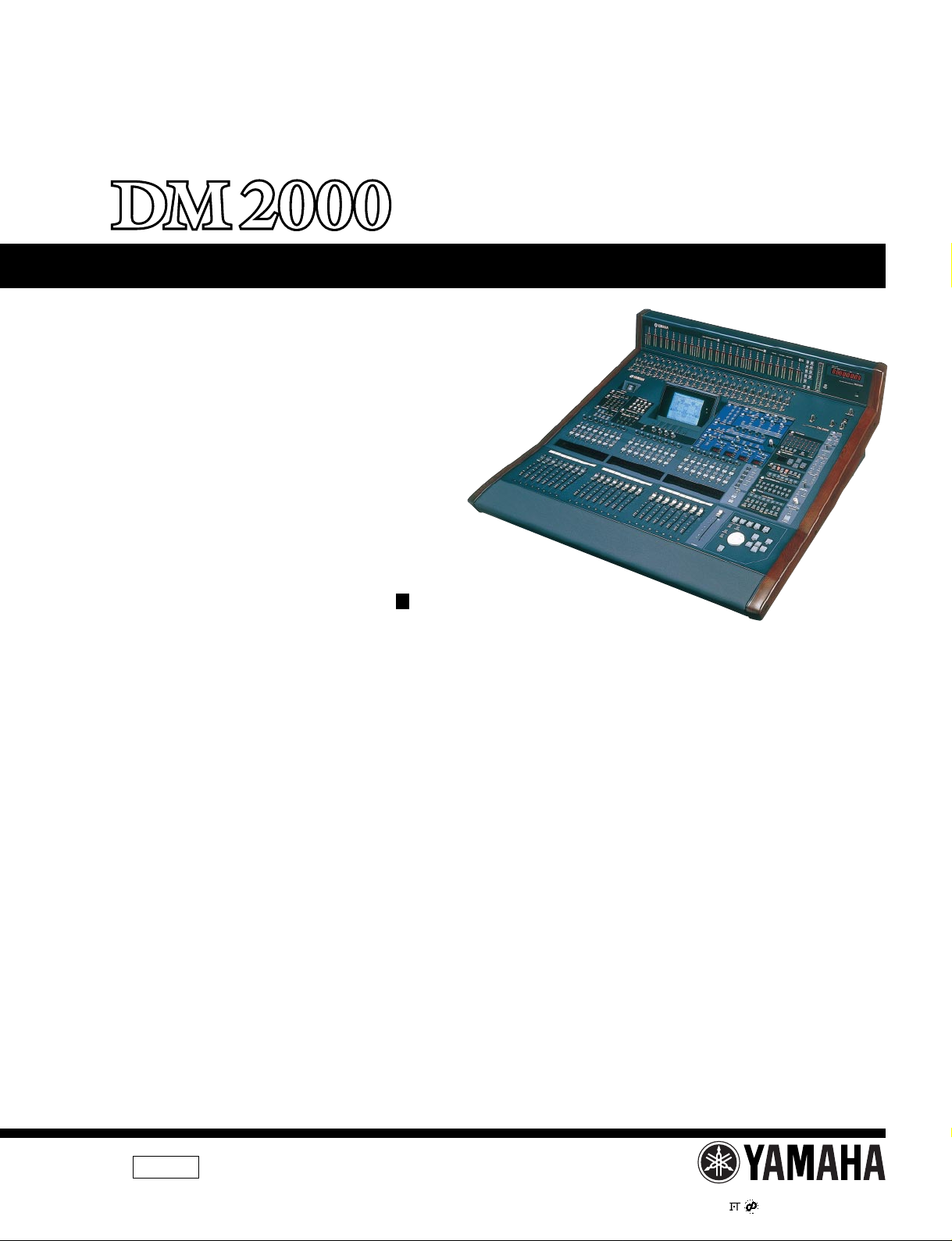
DM2000
/MB2000/SP2000
DIGITAL PRODUCTION CONSOLE/
PEAK METER BRIDGE/WOODEN SIDE PANELS
SERVICE MANUAL
CONTENTS
SPECIFICATIONS ................................................... 4
DIMENSIONS .......................................................... 19
PANEL LAYOUT .................................. 20
CIRCUIT BOARD LAYOUT ............... 36
DISASSEMBLY PROCEDURE ............................ 41
INSTALLING I/O CARDS ....................... 58
LSI PIN DESCRIPTION ................................ 59
IC BLOCK DIAGRAM .................................. 69
CIRCUIT BOARDS ....................................... 77
INSPECTIONS ...................................................142/150
SERVICE CHECK PROGRAM
TEST PROGRAM .........................181/182
USING BULK DUMP ....................... 183
SAVING DM2000 DATA TO SMARTMEDIA
............................ 184
CHECKING THE BATTERY ................ 187
INITIALIZING THE DM2000 ............... 187
MIDI DATA FORMAT ............... 188
MIDI IMPLEMENTATION CHART
............................ 204
PARTS LIST
BLOCK DIAGRAM
OVERALL CONNECTOR CIRCUIT DIAGRAM
.159/170
This document is printed on chlorine free (ECF) paper with soy ink.
011624
PA
OVERALL CIRCUIT DIAGRAM
HAMAMATSU, JAPAN
1.302K-9377 Printed in Japan ’02.03
1
Page 2
DM2000
IMPORTANT NOTICE
This manual has been provided for the use of authorized Yamaha Retailers and their service personnel. It has been assumed
that basic service procedures inherent to the industry, and more specifically Yamaha Products, are already known and understood by the users, and have therefore not been restated.
WARNING : Failure to follow appropriate service and safety procedures when servicing this product may result in per-
IMPORTANT : This presentation or sale of this manual to any individual or firm does not constitute authorization certifi-
The data provided is belived to be accurate and applicable to the unit(s) indicated on the cover. The research engineering, and
service departments of Yamaha are continually striving to improve Yamaha products. Modifications are, therefore, inevitable
and changes in specification are subject to change without notice or obligation to retrofit. Should any discrepancy appear to
exist, please contact the distributor’s Service Division.
WARNING : Static discharges can destroy expensive components. Discharge any static electricity your body may have
IMPORTANT : Turn the unit OFF during disassembly and parts replacement. Recheck all work before you apply power
sonal injury, destruction of expensive components and failure of the product to perform as specified. For
these reasons, we advise all Yamaha product owners that all service required should be performed by an
authorized Yamaha Retailer or the appointed service representative.
cation, recognition of any applicable technical capabilities, or establish a principal-agent relationship of
any form.
accumulated by grounding yourself to the ground bus in the unit (heavy gauge black wires connect to
this bus.)
to the unit.
WARNING: CHEMICAL CONTENT NOTICE!
The solder used in the production of this product contains LEAD. In addition, other electrical/electronic and/or plastic (Where
applicable) components may also contain traces of chemicals found by the California Health and Welfare Agency (and possibly
other entities) to cause cancer and/or birth defects or other reproductive harm.
DO NOT PLACE SOLDER, ELECTRICAL/ELECTRONIC OR PLASTIC COMPONENTS IN YOUR MOUTH FOR ANY REASON WHAT
SO EVER!
Avoid prolonged, unprotected contact between solder and your skin! When soldering, do not inhale solder fumes or expose
eyes to solder/flux vapor!
If you come in contact with solder or components located inside the enclosure of this product, wash your hands before handling
food.
WARNING: THIS APPARATUS MUST BE EARTHED
IMPORTANT
THE WIRES IN THIS MAINS LEAD ARE COLOURED IN
ACCORDANCE WITH THE FOLLOWING CODE:
GREEN-AND-YELLOW : EARTH
BLUE : NEUTRAL
BROWN : LIVE
As the colours of the wires in the mains lead of this apparatus may
not correspond with the coloured markings identifying the terminals in
your plug, proceed as follows:
The wire which is coloured GREEN and YELLOW must be
connected to the terminal in the plug which is marked by the letter E
or by the safety earth symbol or coloured GREEN and YELLOW.
The wire which is coloured BLUE must be connected to the terminal
which is marked with the letter N or coloured BLACK.
The wire which is coloured BROWN must be connected to the
terminal which is marked with the letter L or coloured RED.
* This applies only to products distributed by YAMAHA KEMBLE
MUSIC (U.K.) LTD.
WARNING
Components having special characteristics are marked and must be replaced with parts having specification equal to those
originally installed.
2
Page 3
LITHIUM BATTER Y HANDLING
This product uses a lithium battery for memory back-up.
WARNING : Lithium batteries are dangerous because they can be exploded by improper handling. Observe the following pre-
Leave lithium battery replacement to qualified service personnel.
Always replace with batteries of the same type.
When installing on the PC board by soldering, solder using the connection terminals provided on the battery cells.
Never solder directly to the cells. Perform the soldering as quickly as possible.
Never reverse the battery polarities when installing.
Do not short the batteries.
Do not attempt to recharge these batteries.
Do not disasemble the batteries.
Never heat batteries or throw them into fire.
ADVARSEL!
Lithiumbatteri-Eksplosionsfare ved fejlagtig handtering. Udskiftning ma kun ske med batteri af samme fabrikat og type. lever det brugte
batteri tilbage til leverandren.
VARNING
Explosionsfara vid felaktigt batteribyte.
Anvand samma batterityp eller en ekvivalent typ som rekommenderas av apparattillverkaren.
Kassera anvant batteri enligt fabrikantens instruktion.
VAROITUS
Paristo voi rajahtaa, jos se on virheellisesti asennettu.
Vaihda paristo ainoastaan laitevalmistajan suosittelemaan tyyppiiin.
Havita kaytetty paristo valmistajan ohjeiden mukaisesti.
The following information complies with Dutch official Gazette 1995. 45; ESSENTIALS OF ORDER ON THE COLLECTION OF BATTERIES.
• Please refer to the diassembly procedure for the removal of Back-up Battery.
• Leest u voor het verwijderen van de backup batterij deze beschrijving.
cautions when handling or replacing lithium batteries.
DM2000
Take care not to trap your fingers.
3
Page 4
DM2000
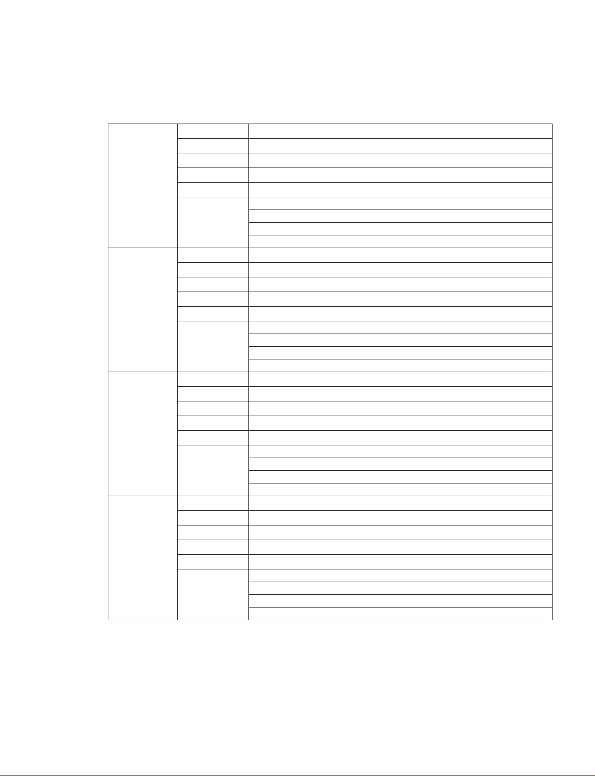
SPECIFICATIONS
DM2000
Number of scene memories
Internal
Sampling Frequency
Signal Delay
Fader
Fader Resolution
Total Harmonic Distortion
(CH INPUT to STEREO OUT)
(Input Gain=Min.)
Frequency Response
(CH INPUT to STEREO OUT)
Dynamic Range
(maximum level to noise level)
Hum & Noise
(20 Hz–20 kHz)
Rs=150
*2
Ω
*1
External
fs=48 kHz
fs=96 kHz
Input Gain=Max.
Input Pad =0 dB
Maximum Voltage Gain
Crosstalk
(@ 1 kHz)
Input Gain=Min.
Phantom switch
Pad switch
Gain control
Peak indicator
AD Input (1–24: A/B)
Analog Input
(2TR IN ANALOG 1, 2)
Option Input (SLOT 1–6) Available cards
Digital Input
(2TR IN DIGITAL 1–3)
Signal indicator
Insert
Insert switch
AD converter
AD converter 24-bit linear, 128-times oversampling (fs=48 kHz)
SRC
99
44.1 kHz, 48 kHz, 88.2 kHz, 96 kHz
Normal rate: 44.1 kHz–10% to 48 kHz+6%
Double rate: 88.2 kHz–10% to 96 kHz+6%
Less than 2.3 ms CH INPUT to STEREO OUT (fs=48 kHz)
Less than 1.2 ms CH INPUT to STEREO OUT (fs=96 kHz)
100 mm motorized with touch sense X 25
+10 to –96, –∞ dB (256 steps/100 mm) input faders
0 to –130, –∞ dB (256 steps/100 mm) master faders, stereo fader
Less than 0.05% 20 Hz to 20 kHz @ +14 dB into 600 Ω
Less than 0.01% 1 kHz @ +18 dB into 600 Ω (fs=48 kHz)
Less than 0.05% 20 Hz to 40 kHz @ +14 dB into 600 Ω
Less than 0.01% 1 kHz @ +18 dB into 600 Ω
20 Hz–20 kHz, 0.5, –1.5 dB @ +4 dB into 600 Ω (fs=48 kHz)
20 Hz–40 kHz, 0.5, –1.5 dB @ +4 dB into 600 Ω (fs=96 kHz)
110 dB typ. DA Converter (STEREO OUT)
108 dB typ. AD+DA (to STEREO OUT) @ fs=48 kHz
106 dB typ. AD+DA (to STEREO OUT) @ fs=96 kHz
–128 dB Equivalent Input Noise
–92 dB residual output noise. STEREO OUT (STEREO OUT off)
–92 dB (96 dB S/N) STEREO OUT (STEREO fader at nominal level and
all CH INPUT faders at minimum level)
–64 dB (68 dB S/N) STEREO OUTPUT (STEREO fader at nominal level
and one CH INPUT fader at nominal level)
74 dB CH INPUT (CH1–24) to STEREO OUT/OMNI (BUS) OUT
74 dB CH INPUT (CH1–24) to OMNI (AUX) OUT (via pre input fader)
74 dB CH INPUT (CH1–24) to CONTROL ROOM MONITOR OUT (via
STEREO bus)
–80 dB adjacent input channels (CH1–24)
–80 dB input to output
+48 V DC is supplied to A (XLR-3-31 type) input
0/26 dB attenuation
44 dB (–60 to –16), detented
LED (red) turns on when post HA level reaches 3 dB below clipping
LED (green) turns on when post HA level reaches 20 dB below nominal
OUT, IN (pre AD converter)
on/off
24-bit linear, 128-times oversampling (fs=48 kHz)
Optional digital interface cards (MY8, MY4 series)
On/off (1:3 and 3:1 maximum input to output sample rate ratio)
4
Page 5
DM2000
Input patch
Phase
Gate-type
Comp-type
Attenuator
EQ
Delay
Input Channel CH1–96
TALKBACK
OSCILLATOR
STEREO OUT DA converter
OMNI OUT 1–8
CONTROL ROOM MONITOR
OUT (LARGE, SMALL)
On/off
Fader
Aux send
Solo
Pan
Surround pan
LFE level
Routing
Direct out
Metering
Level control
AD converter
Talkback select
On/off
Slate
Level
On/off
Waveform
Routing
Output patch
DA converter
Monitor select
Solo contrast
Mono
Dimmer
DA converter
Level control
Phones level
Small trim
*3
—
Normal/reverse
On/off
Key in: 12 ch Group (1–12, 13–24, 25–36, 37–48, 49–60, 61–72,
73–84, 85–96)/AUX1–12
On/off
*4
Key in: self /Stereo Link
Pre EQ/pre fader/post fader
–96.0 to +12.0 dB (0.1 dB step)
4-band PEQ
On/off
0–43400 samples
—
100 mm motorized (INPUT/AUX1–12)
On/off
AUX1–12; pre fader/post fader
On/off
Pre fader/after pan
127 positions (Left= 1–63, Center, Right= 1–63)
127 X 127 positions
∞, –96 dB to +10 dB (256 step)–
STEREO, BUS1–8, DIRECT OUT
Pre EQ/pre fader/post fader
Displayed on LCD
Peak hold on/off
Analog rotary potentiometer
24-bit linear, 128-times oversampling
Built-in microphone/AD IN 1–24
—
On/off
0 to –96 dB (1 dB step)
—
Sine 100 Hz, sine 1 kHz, sine 10 kHz, pink noise, burst noise
BUS1–8, AUX1–12, MATRIX 1L–4R, STEREO L, R
24-bit linear, 128-times oversampling
SURROUND MONITOR, STEREO, BUS1–8, AUX1–12, MATRIX1L–4R,
DIRECT OUT 1–96, INSERT OUT (CH1–96, BUS1–8, AUX1–12,
MATRIX 1L–4R, STEREO)
24-bit linear, 128-times oversampling
STEREO, 2TR IN DIGITAL 1, 2TR IN DIGITAL 2, 2TR IN DIGITAL 3, 2TR
IN ANALOG 1, 2TR IN ANALOG 2, ASSIGN 1, 2 (BUS 1–8/AUX
1–12/MATRIX 1–4)
–96 to 0 dB (1 dB step)
On/off
On/off
24-bit linear, 128-times oversampling
Analog rotary potentiometer
Analog rotary potentiometer
Analog rotary potentiometer
*5
5
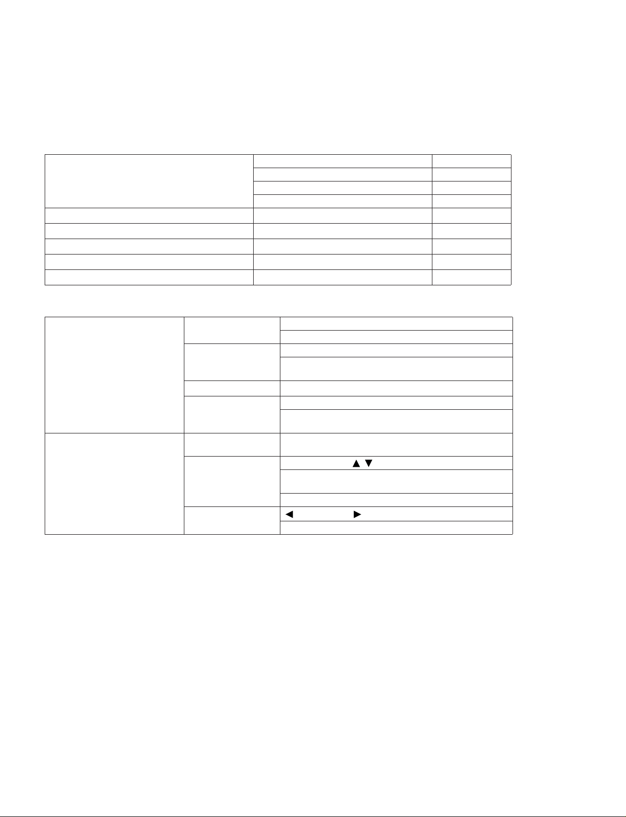
Page 6
DM2000
STUDIO MONITOR OUT
2TR OUT DIGITAL 1–3
Option Output (SLOT 1–6)
Memory card slot
STEREO
BUS1–8
Monitor select
DA converter
Level control
Dither
Output patch
SRC
Available card
Output patch
Dither
Comp-type
*4
Attenuator
EQ
On/off
Fader
Balance
Delay
Matrix send
Metering
Comp-type
*4
Attenuator
EQ
On/off
Fader
Delay
Matrix send
Bus to stereo
Metering
CONTROL ROOM, STEREO, AUX 11, AUX 12
24-bit linear, 128-times oversampling
Analog rotary potentiometer
On/off
Word length 16, 20, 24-bit
STEREO, BUS1–8, AUX 1–12, MATRIX 1L–4R, DIRECT OUT 1–96,
INSERT OUT, CONTROL ROOM
On/off (1:3 and 3:1 maximum input to output sample rate ratio)
Optional digital interface card (MY8, MY4 series)
SURROUND MONITOR, STEREO, BUS1–8, AUX1–12, MATRIX 1L–4R,
DIRECT OUT 1–96, INSERT OUT (CH1–96, BUS1–8, AUX1–12,
MATRIX 1L–4R, STEREO)
On/off
Word length 16/20/24-bit
SmartMedia
On/off
Pre EQ/pre fader/post fader
–96.0 to +12.0 dB (0.1 dB step)
4-band PEQ
*5
On/off
100 mm motorized
127 positions (Left=1–63, Center, Right=1–63)
0–43400 samples
Pre fader/post fader
Level (–∞, –96 dB to +10 dB)
Pan: 127 positions (Left=1–63, Center, Right=1–63)
Displayed on LCD
Peak hold on/off
On/off
Pre EQ/pre fader/post fader
–96.0 to +12.0 dB (0.1 dB step)
4-band PEQ
*5
On/off
—
100 mm motorized
0–43400 samples
Pre fader/post fader
Level (–∞, –96 dB to +10 dB)
Pan: 127 positions (Left=1–63, Center, Right=1–63)
Level (–∞, –130 dB to 0 dB)
On/off
Pan: 127 positions (Left=1–63, Center, Right=1–63)
Displayed on LCD
Peak hold on/off
6
Page 7
On/off
Comp-type
Attenuator
EQ
*4
Pre EQ/pre fader/post fader
–96.0 to +12.0 dB (0.1 dB step)
4-band PEQ
*5
On/off
AUX1–12
On/off
Fader
Delay
—
100 mm motorized
0–43400 samples
Pre fader/post fader
Matrix send
Level (–∞,–96 dB to +10 dB)
Pan: 127 positions (Left=1–63, Center, Right=1–63)
Metering
Comp-type
Attenuator
EQ
Displayed on LCD
Peak hold on/off
On/off
*4
Pre EQ/pre fader/post fader
–96.0 to +12.0 dB (0.1 dB step)
4-band PEQ
*5
On/off
MATRIX 1L–4R
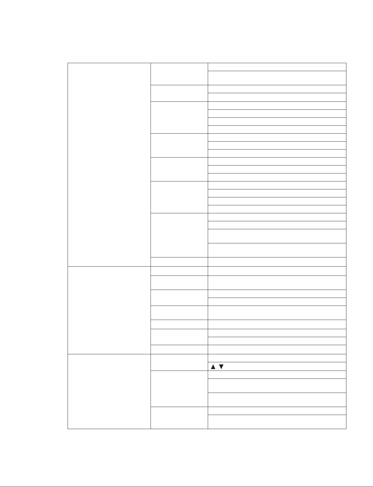
SURROUND MONITOR
INTERNAL EFFECTS
(EFFECT 1–8)
GRAPHIC EQUALIZERS
(GEQ 1–6)
Power Requirements U.S./Canada
On/off
Fader
Balance
Delay
Metering
Mute
Solo
Source
Monitor to C-R
Oscillator
Monitor matrix
Bass
management
Monitor
alignment
Bypass
In/out
Effect-in from
Effect-out to
On/off
Band number
Limit
Insert position
Japan
—
100 mm motorized
127 positions (Left=1–63, Center, Right=1–63)
0–43400 samples
Displayed on LCD
Peak hold on/off
On/off
On/off
BUS1–8, SLOT 1–6
On/off
Pink noise/500–2 kHz/1 kHz
5.1→5.1, 5.1→3-1, 5.1→ST, 3.1→3.1, 3.1→ST
5 presets
ATT (–12.0 dB to 12 dB 0.1 dB step), Delay (0–30.0 msec 0.01 msec
step)
On/off
8-in, 8-out (EFFECT1–2): depends on effects type
2-in, 2-out (EFFECT3–8): depends on effects type
AUX1–12/INSERT OUT/effect-out
Input patch/effect-in
—
31
±15 dB, ±12 dB, ±6 dB, –24 dB
BUS1–8/AUX1–12/STEREO L, R/MATRIX 1L–4R
100 V, 50/60 Hz 230 W WITH OPTION 230 W WITHOUT OPTION 165 W
120 V, 60 Hz 300 W
Other 220–240 V, 50/60 Hz 300 W
Dimensions (H x D x W) 257 x 821 x 906 mm (10.1" x 32.3" x 35.7")
Net weight
Operating free-air temperature range
Storage temperature range
43 kg (94.8 lbs)
10–35°C (50–95°F)
–20 to 60°C (–4 to 140°F)
DM2000
7
Page 8
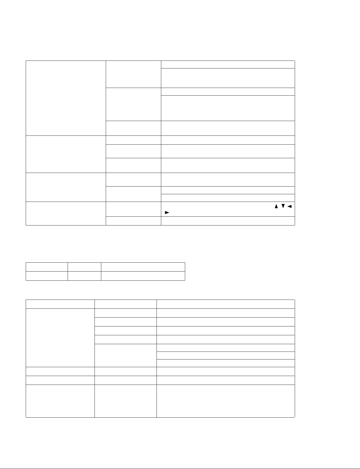
DM2000
Supplied Accessories
Options
*1. Total harmonic distortion is measured with a 6 dB/octave filter @ 80 kHz.
*2. Hum & Noise are measured with a 6 dB/octave filter @ 12.7 kHz; equivalent to a 20 kHz filter with infinite dB/octave
attenuation.
*3. See “Gate Parameters” on page 8.
*4. See “Comp Parameters” on page 9.
*5. See “EQ Parameters” on page 8.
AC Cable
CD-ROM (Studio Manager)
Digital interface card (MY8, MY4 series)
PEAK METER BRIDGE: MB2000
SIDE PANEL: SP2000
EQ Parameters
LOW/HPF L-MID H-MID HIGH /LPF
0.1–10.0
Q
F
G
(41 points)
low shelving
HPF
21.2 Hz–20 kHz (1/12 oct step)
±18 dB
(0.1 dB step)
HPF: on/off
0.1–10.0
(41 points)
±18 dB
(0.1 dB step)
high shelving
Gate Parameters
0.1–10.0
(41 points)
LPF
±18 dB
(0.1 dB step)
LPF: on/off
Gate
Ducking
Threshold
Range
Attack
Hold
Decay
Threshold
Range
Attack
Hold
Decay
–54 dB to 0 dB (0.1 dB step)
–70 dB to 0 dB (1 dB step)
0 ms–120 ms (1 ms step)
0.02 ms–1.96 s (216 points) @ 48 kHz
0.02 ms–2.13 s (216 points) @ 44.1 kHz
0.01 ms–981 ms (216 points) @ 96 kHz
0.01 ms–1.06 s (216 points) @ 88.2 kHz
5 ms–42.3 s (160 points) @ 48 kHz
6 ms–46.0 s (160 points) @ 44.1 kHz
3 ms–21.1 s (160 points) @ 96 kHz
3 ms–23.0 s (160 points) @ 88.2 kHz
8
Page 9
Comp Parameters
DM2000
Compressor
Expander
Compander H
Compander S
Threshold
Ratio (x :1)
Out gain
Knee
Attack
Release
Threshold
Ratio (x :1)
Out gain
Knee
Attack
Release
Threshold
Ratio (x :1)
Out gain
Width
Attack
Release
Threshold
Ratio (x :1)
Out gain
Width
Attack
Release
–54 dB to 0 dB (0.1 dB step)
x=1, 1.1, 1.3, 1.5, 1.7, 2, 2.5, 3, 3.5, 4, 5, 6, 8, 10, 20, ∞ (16 points)
0 dB to +18 dB (0.1 dB step)
Hard, 1, 2, 3, 4, 5 (6 step)
0 ms–120 ms (1 ms step)
5 ms–42.3 s (160 points) @ 48 kHz
6 ms–46.0 s (160 points) @ 44.1 kHz
3 ms–21.1 s (160 points) @ 96 kHz
3 ms–23.0 s (160 points) @ 88.2 kHz
–54 dB to 0 dB (0.1 dB step)
x=1, 1.1, 1.3, 1.5, 1.7, 2, 2.5, 3, 3.5, 4, 5, 6, 8, 10, 20, ∞ (16 points)
0 dB to +18 dB (0.1 dB step)
Hard, 1, 2, 3, 4, 5 (6 points)
0 ms–120 ms (1 ms step)
5 ms–42.3 s (160 points) @ 48 kHz
6 ms–46.0 s (160 points) @ 44.1 kHz
3 ms–21.1 s (160 points) @ 96 kHz
3 ms–23.0 s (160 points) @ 88.2 kHz
–54 dB to 0 dB (0.1 dB step)
x=1, 1.1, 1.3, 1.5, 1.7, 2, 2.5, 3, 3.5, 4, 5, 6, 8, 10, 20, ∞ (16 points)
–18 dB to 0 dB (0.1 dB step)
1 dB–90 dB (1 dB step)
0 ms–120 ms (1 ms step)
5 ms–42.3 s (160 points) @ 48 kHz
6 ms–46.0 s (160 points) @ 44.1 kHz
3 ms–21.1 s (160 points) @ 96 kHz
3 ms–23.0 s (160 points) @ 88.2 kHz
–54 dB to 0 dB (0.1 dB step)
x=1, 1.1, 1.3, 1.5, 1.7, 2, 2.5, 3, 3.5, 4, 5, 6, 8, 10, 20 (15 points)
–18 dB to 0 dB (0.1 dB step)
1 dB–90 dB (1 dB step)
0 ms–120 ms (1 ms step)
5 ms–42.3 s (160 points) @ 48 kHz
6 ms–46.0 s (160 points) @ 44.1 kHz
3 ms–21.1 s (160 points) @ 96 kHz
3 ms–23.0 s (160 points) @ 88.2 kHz
9
Page 10
DM2000
Controls
Analog Section
INPUT 1–24
TALKBACK
STUDIO MONITOR OUT
CONTROL ROOM MONITOR OUT
CONTROL ROOM MONITOR OUT SMALL
PHONES
Digital Section
FADER MODE Section
DISPLAY CONTROL Section
+48 V switch ON/OFF
PAD switch 0/26 dB
GAIN control –16 to –60 dB
INSERT switch ON/OFF
TALKBACK LEVEL control
STUDIO LEVEL control
CONTROL ROOM LEVEL control
SMALL TRIM control
PHONES LEVEL control
MATRIX SELECT
AUX SELECT
FADER MODE
ENCODER MODE
DISPLAY buttons
EFFECTS/PLUG-INS
Others
DISPLAY button
MATRIX 1, MATRIX 2, MATRIX 3, MATRIX 4 buttons (w/LED)
DISPLAY button
AUX 1, AUX 2, AUX 3, AUX 4, AUX 5, AUX 6, AUX 7, AUX 8,
AUX 9, AUX 10, AUX 11, AUX 12 buttons (w/LED)
FADER, AUX/MTRX button (w/LED)
DISPLAY button
PAN, AUX/MTRX, ASSIGN 1, ASSIGN 2, ASSIGN 3, ASSIGN 4
buttons (w/LED)
DATA, DIO, SETUP, UTILITY, MIDI, REMOTE, METER, VIEW,
PAIR, GROUP, INPUT PATCH, OUTPUT PATCH
DISPLAY access, ,
INTERNAL EFFECTS, GRAPHIC EQUALIZERS, PLUG-INS,
CHANNEL INSERTS 1, 2, 3, 4, 5, 6, 7, 8
Parameter control: 1, 2, 3, 4
, F1, F2, F3, F4,
LCD contrast control
buttons
10
Page 11
SELECTED CHANNEL Section
MONITOR Section
SCENE MEMORY, AUTOMIX and
USER DEFINED KEYS section
ROUTING
PHASE/INSERT
DELAY
AUX/MATRIX SEND
DYNAMICS
PAN/SURROUND
EQUALIZER
CH COPY/PASTE
MONITOR
STUDIO
SOLO
CONTROL ROOM
SURROUND
Others
TALKBACK
SCENE MEMORY
AUTOMIX
USER DEFINED KEYS
DM2000
DISPLAY button
1, 2, 3, 4, 5, 6, 7, 8, STEREO, DIRECT, FOLLOW PAN buttons
(w/LED)
DISPLAY button
ø
, INSERT ON buttons (w/LED)
DISPLAY button
ON button (w/LED)
TIME control
MIX/FB control (w/SW)
DISPLAY, BANK button
ON button (w/LED) x 4
LEVEL control (w/SW) x 4
DISPLAY, GATE /COMP buttons
GATE ON, COMP ON buttons (w/LED)
Parameter control x 5
DISPLAY button
L, R, LINK, GRAB, EFFECT buttons (w/LED)
Pan control
Joystick (Sound image position control)
DISPLAY button
EQ ON button (w/LED)
ATT control, GAIN controls: LOW, LOW-MID, HIGH-MID,
HIGH
FREQUENCY/Q controls: LOW, LOW-MID, HIGH-MID, HIGH
controls (w/SW)
COPY, PASTE buttons
DISPLAY button
CONTROL ROOM, STEREO, AUX 11, AUX 12 buttons
(w/LED)
CLEAR button
SOLO CONTRAST control
STEREO: 2TR D1, 2TR D2, 2TR D3, 2TR A1, 2TR A2, STEREO,
ASSIGN 1, ASSIGN 2 buttons (w/LED)
BUS, ASSIGN 1, ASSIGN 2 buttons (w/LED)
SURROUND MONITOR LEVEL control
MONO, DIMMER, SMALL buttons (w/LED)
SLATE, TALKBACK buttons (w/LED)
DISPLAY button
, , STORE, RECALL buttons
DISPLAY button
ENABLE, REC, ABORT/UNDO, AUTOREC, RETURN, RELATIVE,
TOUCH SENSE buttons (w/LED)
OVERWRITE parameters: FADER, ON, PAN, SURROUND, AUX,
AUX ON, EQ buttons (w/LED)
DISPLAY button
1, 2, 3, 4, 5, 6, 7, 8, 9, 10, 11, 12, 13, 14, 15, 16 buttons
(w/LED)
11
Page 12
DM2000
MACHINE CONTROL Section
CHANNEL STRIP Section
MASTER Section
DATA ENTRY Section
TRACK ARMING
LOCATOR
TRANSPORT
CONTROL
Encoders
Buttons
Faders (w/ touch
sense)
LAYER
STEREO
Buttons
Encoder
DISPLAY, ALL CLEAR buttons
1, 2, 3, 4, 5, 6, 7, 8, 9, 10, 11, 12, 13, 14, 15, 16, 17, 18, 19,
20, 21, 22, 23, 24, MASTER, TRACK ARMING GROUP: A, B, C,
D buttons (w/LED)
DISPLAY button
LOCATE MEMORY: 1, 2, 3, 4, 5, 6, 7, 8, AUDITION, PRE, IN,
OUT, POST, SET, MTR, RETURN TO ZERO, END, ONLINE,
LOOP, QUICK PUNCH, ROLL BACK, REHEARSAL, MASTER buttons (w/LED)
REW, FF, STOP, PLAY, REC, SHUTTLE, SCRUB (w/LED)
x 24 (1–24)
AUTO x 24 (1–24), SEL x 24 (1–24), SOLO x 24 (1–24), ON x
24 (1–24)
x 24 (1–24)
Input CH: 1–24, 25–48, 49–72, 73–96, MASTER, REMOTE 1,
REMOTE 2, REMOTE 3, REMOTE 4 buttons (w/LED)
AUTO, SEL, ON buttons (w/LED)
Fader (w/touch sense) x 1
DISPLAY HISTORY: BACK, FORWARD, INC, DEC, , , ,
, ENTER buttons
Parameter wheel
Indicators
Analog Section
PEAK LED
SIGNAL LED
x24 INPUT 1–24
x24 INPUT 1–24
Digital Section
DISPLAY CONTROL Section
SELECTED CHANNEL Section
MONITOR Section SOLO
SCENE MEMORY section Scene memory number
CHANNEL STRIP Section
DISPLAY
DELAY
AUX / MATRIX SEND
DYNAMICS
PAN/SURROUND
EQUALIZER
CH NAME, routing,
panning position, EQ,
INS, DLY, COMP, GATE:
on/ off, touch sense
status, etc
320 X 240 dot graphic LCD (w/contrast control potentiometer)
MIX, FB LEDs x2
BANK LEDs x3
GATE, COMP LEDs x2
Pan position LEDs x10
FREQUENCY, Q LEDs 2 X 4
dB, Hz, kHz 3 X 4
3-digit numeric LEDs x4 (parameter value)
LED x1
2-digit numeric LED x1
2 color VFD (FL) units x3
12
Page 13
Effect library (EFFECT 1–8)
Presets 52 (EFFECT 3–8: 44)
User memories 76
Compressor library
Presets 36
User memories 92
Gate library
Presets 4
User memories 124
EQ library
Presets 40
User memories 160
Channel library
Presets 2
User memories 127
GEQ library (GEQ 1–6)
Presets 1
User memories 128
Surround Monitor library
Presets 1
User memories 32
Input patch library
Presets 1
User memories 32
Output patch library
Presets 1
User memories 32
Bus to Stereo library
Presets 1
User memories 32
Libraries
DM2000
13
Page 14
DM2000
Analog Input Spec
Input level
*1
Nominal
–60 dB
(0.775 mV)
–16 dB
(0.123 V)
+10 dB
(2.45 V)
(1.23 V)
(1.23 V)
–10 dBV
(0.316 V)
+4 dB
+4 dB
Max.
before clip
–46 dB
(3.88 mV)
–2 dB
(616 mV)
+24 dB
(12.28 V)
+18 dB
(6.16 V)
+18 dB
(6.16 V)
+4 dBV
(1.58 V)
A: XLR-3-31 type (Balanced)
B: Phone jack
(TRS)(Balanced)
Phone jack (TRS) (Balanced)
Phone jack (TRS) (Balanced)
Phono (Unbalanced)
Input PAD GAIN
INPUT A/B 1–24
INSERT IN 1–24
2TR IN ANALOG
1 [L, R]
2TR IN ANALOG
2 [L, R]
Actual Load
–60
dB
0
–16
dB
26
— 10K Ω
— 10K Ω
— 10K Ω
Impedance
3k Ω
For Use
With
Nominal
50–600 Ω
Mics &
600 Ω
Lines
600 Ω
Lines
600 Ω
Lines
600 Ω
Lines
Sensitivity
–70 dB
(0.245 mV)
–26 dB
(38.8 mV)
0dB
(775 mV)
–6dB
(388 mV)
+4 dB
(1.23 V)
–10 dBV
(0.316 V)
*1. Sensitivity is the lowest level that will produce an output of +4 dB (1.23 V) or the nominal output level when the unit
is set to maximum gain. (All faders and level controls are maximum position.)
*2. XLR-3-31 type connectors are balanced (1=GND, 2=HOT, 3=COLD).
*3. Phone jacks are balanced (Tip=HOT, Ring=COLD, Sleeve=GND).
In these specifications, when dB represents a specific voltage, 0 dB is referenced to 0.775 Vrms.
For 2TR IN ANALOG 1, 2 levels, 0 dBV is referenced to 1.00 Vrms.
All input AD converters (except INSERT IN 1–24) are 24-bit linear, 128-times oversampling.
+48 V DC (phantom power) is supplied to CH INPUT (1–24) XLR type connectors via individual switches.
Connector
*2
*3
*3
*3
Analog Output Spec
Output
STEREO OUT [L, R]
STUDIO MONITOR OUT
[L, R]
C-R MONITOR OUT LARGE
[L, R]
C-R MONITOR OUT SMALL
[L, R]
OMNI OUT 1–8
INSERT OUT 1–24
PHONES
*1. XLR-3-32 type connectors are balanced (1=GND, 2=HOT, 3=COLD).
*2. Phone jacks are balanced (Tip=HOT, Ring=COLD, Sleeve=GND).
*3. PHONES stereo phone jack is unbalanced (Tip=LEFT, Ring=RIGHT, Sleeve=GND).
STEREO OUT [L, R], 0 dBV is referenced to 1.00 Vrms.
In these specifications, when dB represents a specific voltage, 0 dB is referenced to 0.775 Vrms.
All output DA converters (except INSERT OUT 1–24) are 24-bit, 128-times oversampling.
14
Actual Source
Impedance
For Use
With
Nominal
600 Ω 10k Ω Lines —
150 Ω 600 Ω Lines —
150 Ω 10k Ω Lines —
150 Ω 600 Ω Lines —
150 Ω 600 Ω Lines —
150 Ω 10k Ω Lines
600 Ω 10k Ω Lines —
100 Ω
8 Ω Lines — 4 mW 25 mW
40 Ω Lines — 12 mW 75 mW
GAIN SW
+18 dB
(default)
+4 dB
Output level
Nominal
–10 dBV
(0.316 V)
+4 dB
(1.23 V)
+4 dB
(1.23 V)
+4 dB
(1.23 V)
+4 dB
(1.23 V)
+4 dB
(1.23 V)
–10 dB
(0.245 V)
+4 dB
(1.23 V)
Max. before
clip
+4 dBV
(1.58 V)
+18 dB
(6.16 V)
+18 dB
(6.16 V)
+18 dB
(6.16 V)
+18 dB
(6.16 V)
+18 dB
(6.16 V)
+4 dB
(1.23 V)
+18 dB
(6.16 V)
Connector
Phono (Unbalanced)
XLR-3-32 type (Bal-
*1
anced)
Phone Jack (TRS) (Bal-
*2
anced)
XLR-3-32 type (Bal-
*1
anced)
XLR-3-32 type (Bal-
*1
anced)
Phone Jack (TRS) (Bal-
*2
anced)
Phone Jack (TRS) (Bal-
*2
anced)
Stereo Phone Jack (TRS)
(Unbalanced)
*3
Page 15
g
Digital Input Spec
Input Format Data length Level Connector
2TR IN DIGITAL
CASCADE IN
1
2
3
AES/EBU 24-bit RS422
AES/EBU 24-bit RS422
IEC-60958 24-bit 0.5 Vpp/75 Ω PHONO
— — RS422
*1. XLR-3-31 type connectors are balanced (1=GND, 2=HOT, 3=COLD).
Digital Output Spec
Output Format Data length Level Connector
1
2TR OUT DIGITAL
2
3
CASCADE OUT
*1. Channel status of 2TR OUT DIGITAL 1, 2
Type: 2 audio channels
Emphasis: NO
Sampling rate: depends on the internal configuration
AES/EBU
Professional use
AES/EBU
Professional use
IEC-60958
Consumer use
*1
*1
*4
— — RS422
24-bit
24-bit
24-bit
XLR-3-31 type (Balanced)
XLR-3-31 type (Balanced)
D-SUB Half Pitch Connector 68P
(Female)
*2
*2
*2
RS422
RS422
0.5V pp/75 Ω Phono
DM2000
*1
*1
XLR-3-32 type (Balanced)
XLR-3-32 type (Balanced)
D-SUB Half Pitch Connector 68P (Female)
*3
*3
*2. Dither: word length 16/20/24 bit
*3. XLR-3-32 type connectors are balanced (1=GND, 2=HOT, 3=COLD).
*4. Channel status of 2TR OUT DIGITAL 3
Type: 2 audio channels
Category code: 2 channel PCM encoder/decoder
Copy prohibit: NO
Emphasis: NO
Clock accuracy: Level II (1000 ppm)
Samplin
rate: depends on the internal configuration
15
Page 16
DM2000
I/O Slot Spec
Each I/O SLOT accepts a digital interface card. Only SLOT #1 has a serial interface.
Card Name Function Accept Input Output
MY8-AT
MY8-TD
MY8-AE
MY4-AD
MY8-AD
MY4-DA
MY8-AD24
MY8-AD96
MY8-DA96
MY8-AE96S
MY8-AE96
*1. See the Digital I/O chapter.
Details depend on each interface card.
ADAT YES 8 IN
TASCAM YES 8 IN
AES/EBU YES 8 IN
ANALOG IN YES 4 IN — 6
ANALOG IN YES 8 IN — 6
ANALOG OUT YES —
ANALOG IN YES 8 IN — 6
ANALOG IN YES 8 IN — 6
ANALOG OUT YES —
AES/EBU YES 8 IN
AES/EBU YES 8 IN
8 OUT (depends on output
*1
patch)
8 OUT (depends on output
*1
patch)
8 OUT (depends on output
*1
patch)
4 OUT (depends on output
*1
patch)
8 OUT (depends on output
*1
patch)
8 OUT (depends on output
*1
patch)
8 OUT (depends on output
*1
patch)
Number of
available cards
6
6
6
6
6
4
6
Control I/O Spec
I/O Port Format Level Connector in Console
TO HOST
MIDI
TIME CODE IN
WORD CLOCK
CONTROL
REMOTE
KEYBOARD
STORAGE CARD
METER
*1. XLR-3-31 type connectors are balanced (1=GND, 2=HOT, 3=COLD).
*2. This switch is on the rear panel.
Serial
USB
IN
OUT
THRU
MTC
SMPTE
IN
OUT 1, 2
— RS422 Mini DIN Connector 8P
USB 1.1 0 V–3.3 V B type USB connector
MIDI — DIN Connector 5P
MIDI — DIN Connector 5P
MIDI — DIN Connector 5P
MIDI — DIN Connector 5P
SMPTE Nominal –10 dB/10k Ω
—
— TTL/75 Ω BNC Connector
— — D-SUB Connector 25P (Female)
— RS422 D-SUB Connector 9P (Male)
PS/2 — DIN Connector 6P
— — SmartMedia slot
— RS422 D-SUB Connector 15P (Female)
TTL/75 Ω (ON/OFF)
XLR-3-31 type (Balanced)
*2
BNC Connector
*1
16
Page 17
DM2000
Connector Pin Assignments
CASCADE IN CASCADE OUT
Pin Signal Signal Signal SignalPin Pin Pin
1 GND 35 GND 1 GND 35 GND
2 INPUT 1-2(+) 36 INPUT 1-2(–) 2 OUTPUT 1-2(+) 36 OUTPUT 1-2(–)
3 INPUT 3-4(+) 37 INPUT 3-4(–) 3 OUTPUT 3-4(+) 37 OUTPUT 3-4(–)
4 INPUT 5-6(+) 38 INPUT 5-6(–) 4 OUTPUT 5-6(+) 38 OUTPUT 5-6(–)
5 INPUT 7-8(+) 39 INPUT 7-8(–) 5 OUTPUT 7-8(+) 39 OUTPUT 7-8(–)
6 INPUT 9-10(+) 40 INPUT 9-10(–) 6 OUTPUT 9-10(+) 40 OUTPUT 9-10(–)
7 INPUT 11-12(+) 41 INPUT 11-12(–) 7 OUTPUT 11-12(+) 41 OUTPUT 11-12(–)
8 INPUT 13-14(+) 42 INPUT 13-14(–) 8 OUTPUT 13-14(+) 42 OUTPUT 13-14(–)
9 INPUT 15-16(+) 43 INPUT 15-16(–) 9 OUTPUT 15-16(+) 43 OUTPUT 15-16(–)
10 DTR IN(+) 44 DTR IN(–) 10 DTR OUT(+) 44 DTR OUT(–)
11 RTS OUT(+) 45 RTS OUT(–) 11 RTS IN(+) 45 RTS IN(–)
12 GND 46 GND 12 GND 46 GND
13 WORD CLOCK IN(+) 47 WORD CLOCK IN(–) 13 WORD CLOCK OUT(+) 47 WORD CLOCK OUT(–)
14 WORD CLOCK OUT(+) 48 WORD CLOCK OUT(–) 14 WORD CLOCK IN(+) 48 WORD CLOCK IN(–)
15 CONTROL IN(+) 49 CONTROL IN(–) 15 CONTROL OUT(+) 49 CONTROL OUT(–)
16 CONTROL OUT(+) 50 CONTROL OUT(–) 16 CONTROL IN(+) 50 CONTROL IN(–)
17 GND 51 ID6 IN 17 GND 51 ID6 OUT
18 GND 52 ID6 OUT 18 GND 52 ID6 IN
19 INPUT 17-18(+) 53 INPUT 17-18(–) 19 OUTPUT 17-18(+) 53 OUTPUT 17-18(–)
20 INPUT 19-20(+) 54 INPUT 19-20(–) 20 OUTPUT 19-20(+) 54 OUTPUT 19-20(–)
21 INPUT 21-22(+) 55 INPUT 21-22(–) 21 OUTPUT 21-22(+) 55 OUTPUT 21-22(–)
22 INPUT 23-24(+) 56 INPUT 23-24(–) 22 OUTPUT 23-24(+) 56 OUTPUT 23-24(–)
23 RESERVED 57 RESERVED 23 RESERVED 57 RESERVED
24 RESERVED 58 RESERVED 24 RESERVED 58 RESERVED
25 RESERVED 59 RESERVED 25 RESERVED 59 RESERVED
26 RESERVED 60 RESERVED 26 RESERVED 60 RESERVED
27 ID0 IN 61 ID1 IN 27 ID0 OUT 61 ID1 OUT
28 ID2 IN 62 ID3 IN 28 ID2 OUT 62 ID3 OUT
29 ID4 IN 63 ID5 IN 29 ID4 OUT 63 ID5 OUT
30 ID0 OUT 64 ID1 OUT 30 ID0 IN 64 ID1 IN
31 ID2 OUT 65 ID3 OUT 31 ID2 IN 65 ID3 IN
32 ID4 OUT 66 ID5 OUT 32 ID4 IN 66 ID5 IN
33 MSB IN 67 2CH/LINE IN 33 MSB OUT 67 2CH/LINE OUT
34 FG 68 FG 34 FG 68 FG
17
Page 18
DM2000
REMOTE Port
Pin Pin
1 GND 6
2
3
4
5 N.C.
Signal
RX+/GND
RX–/RX–
TX–/TX+
TX+/GND
*1. RS422 (for AD824)/SONY 9-pin protocol (P2).
*1
*1
*1
7
RTS/RX+
8
CTS/TX–
9 GND
CONTROL Port
Pin Pin
1 GPO0 14 GPO1
2 GPO2 15 GPO3
3 GPO4 16 GPO5
4 GPO6 17 GPO7
5 GND 18 GND
6 GND 19 GND
7 GND 20 GND
8 GND 21 +5V
9 +5V 22 GPI0
10 GPI1 23 N.C.
11 N.C. 24
12
13
Signal Signal
*1
SMODE
*1
SPARE
*1. For 02R SOLO control.
25
SOLO
MAS/SLV
Signal
*1
*1
*1
*1
*1
MB2000
Dimensions (W X H X D) : 904.0 X 123.5 X 95.0 mm
Weight : 3.8 kg
18
Page 19
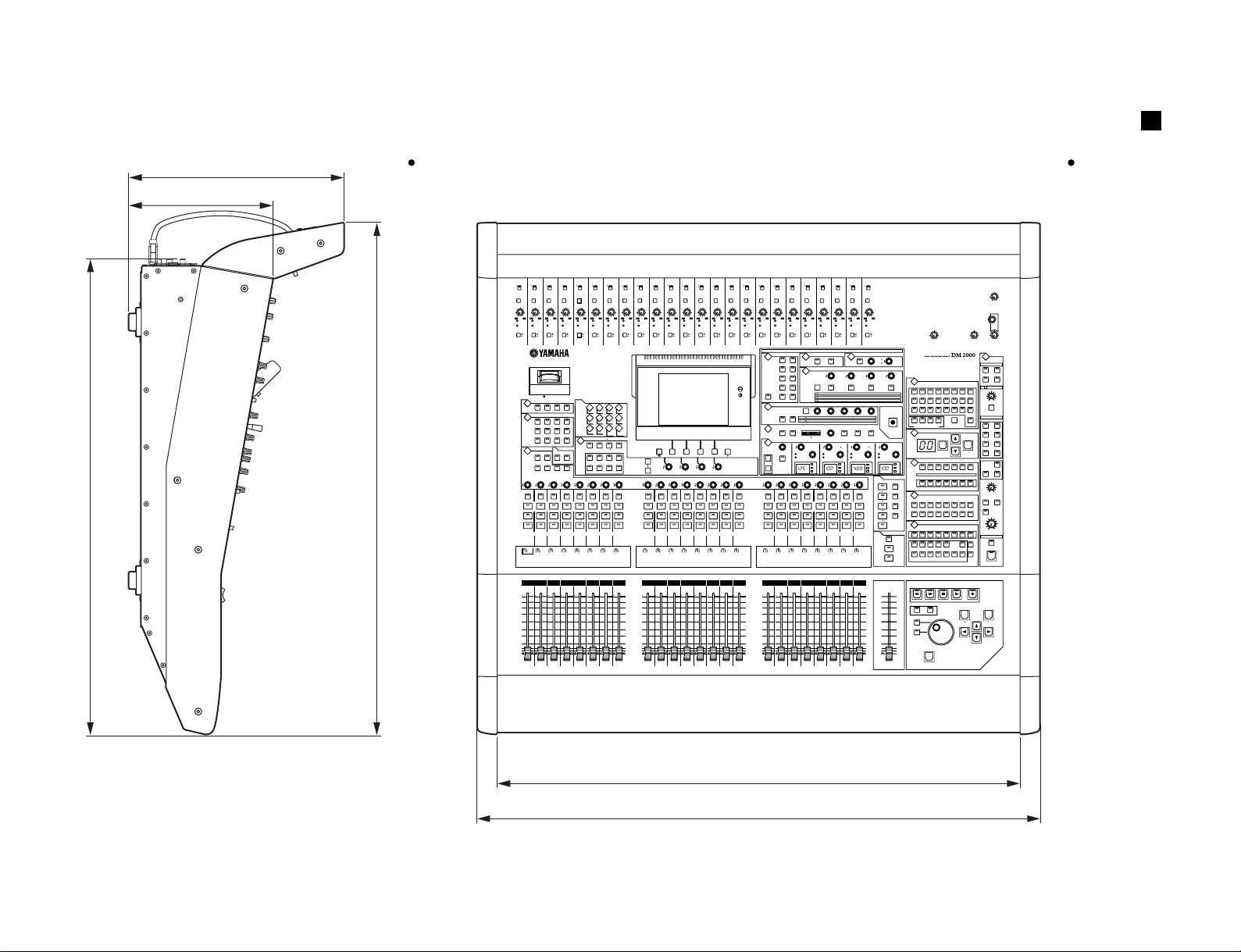
DIMENSIONS
820.8 mm
247 mm
371 mm
Side view
883.2 mm
+
48V+48V+48V+48V+48V+48V+48V+48V+48V+48V+48V+48V+48V+48V+48V+48V+48V+48V+48V+48V+48V+48V+48V+48V
ON
OFF
PAD
26dB
26dB
-
60
-
16
-
16
GAIN
GAIN
PEAK
PEAK
SIGNAL
SIGNAL
234
1
OFF
ON
INSERT
INSERT
DISPLAY
MATRIX1
DISPLAY
DISPLAY
AUTO
SEL
SOLO
ON
ON
OFF
-
60
OFF
ON
MATRIXSELECT
AUXSELECT
ENCODER MODE
PAN
PAN SEND LEVEL
AUTO
SEL
SOLO
ON
ON
OFF
26dB
-
16
GAIN
PEAK
SIGNAL
INSERT
3.3V
CARD
MATRIX2 MATRIX4MATRIX3
AUX2AUX1 AUX 3 AUX4
AUX6AUX5 AUX 7
AUX10AUX9 AUX11
AUX/MTRX
ASSIGN2ASSIGN1
AUTO
SEL
SOLO
ON
ON
ON
OFF
OFF
26dB
26dB
26dB
-
60
-
60
-
60
-
16
-
16
-
16
GAIN
GAIN
GAIN
PEAK
PEAK
PEAK
SIGNAL
SIGNAL
SIGNAL
5
6
OFF
OFF
OFF
ON
ON
ON
INSERT
INSERT
INSERT
DISPLAYACCESS
DATA DIO SETUP UTILITY
MIDI REMOTE METER VIEW
PAIR GROUP INPUT
AUX8
EFFECTS/PLUG INS
AUX12
DISPLAY
INTERNAL
GRAPHIC
FADER MODE
EFFECTS
EQUALIZERS
AUX/MTR X
FADER
1234
ASSIGN4ASSIGN3
5678
INSERTSENDASSIGNOUTPUTINPUT
AUTO
AUTO
AUTO
SEL
SEL
SEL
SOLO
SOLO
SOLO
ON
ON
ON
ON
ON
ON
ON
OFF
OFF
OFF
OFF
-
60
SIGNAL
OFF
ON
PLUGINS
AUTO
SEL
SOLO
ON
26dB
26dB
26dB
26dB
-
60
-
60
-
60
-
16
-
16
-
16
-
16
PEAK
INSERT
PATCH
GAIN
GAIN
GAIN
GAIN
PEAK
PEAK
PEAK
SIGNAL
SIGNAL
SIGNAL
78
910 21 22 23 24
OFF
OFF
OFF
ON
ON
ON
INSERT
INSERT
INSERT
OUTPUT
PATCH
CHANNEL
INSERTS
AUTO
AUTO
SEL
SEL
SOLO
SOLO
ON
ON
87654321 9 10111213141516 1718192021222324
ON
ON
ON
OFF
OFF
OFF
26dB
26dB
26dB
-
60
-
60
-
60
-
16
-
16
-
16
GAIN
GAIN
GAIN
PEAK
PEAK
PEAK
SIGNAL
SIGNAL
SIGNAL
11
12 13 14 15
OFF
OFF
OFF
ON
ON
ON
INSERT
INSERT
INSERT
F1 F2 F3
1234
AUTO
AUTO
AUTO
AUTO
SEL
SEL
SEL
SEL
SOLO
SOLO
SOLO
SOLO
ON
ON
ON
ON
ON
OFF
26dB
-
60
-
16
GAIN
PEAK
SIGNAL
OFF
ON
INSERT
F4
AUTO
SEL
SOLO
ON
ON
ON
ON
ON
OFF
OFF
OFF
OFF
-
60
-
16
PEAK
SIGNAL
OFF
ON
INSERT
AUTO
SEL
SOLO
ON
26dB
26dB
26dB
26dB
-
60
-
60
-
60
-
16
-
16
-
16
GAIN
GAIN
GAIN
GAIN
PEAK
PEAK
PEAK
SIGNAL
SIGNAL
SIGNAL
16
18 19 20
17
OFF
OFF
OFF
ON
ON
ON
INSERT
INSERT
INSERT
ROUTING
DISPLAY
DYNAMICS
DISPLAY
PAN/ SURROUND
DISPLAY
EQUALIZER
DISPLAY
CHANNEL
COPY
PASTE
AUTO
AUTO
SEL
SEL
SOLO
SOLO
ON
ON
ON
OFF
-
60
OFF
ON
12
34
56
78
STEREOFOLLOWPAN DIRECT
GATEON COMP ON
L
ATT.
EQON
AUTO
SEL
SOLO
ON
ON
OFF
26dB
-
16
GAIN
PEAK
SIGNAL
INSERT
R
AUTO
SEL
SOLO
ON
ON
ON
OFF
OFF
26dB
26dB
-
60
-
60
-
60
-
16
-
16
GAIN
GAIN
PEAK
PEAK
SIGNAL
SIGNAL
SIGNAL
OFF
OFF
OFF
ON
ON
ON
INSERT
INSERT
SELECTED CHANNEL
PHASE/ INSERT
DISPLAY
INSERTON
AUX/ MATRIXSEND
DISPLAY
BANK
ON
AUX1/MATRIX 1
AUX5
AUX9
GATE/COMP
RANGE
THRESHOLD HOLD
GATE
COMP
RATIO
L
R
EVEN
ODD
LOW
FREQUENCY
FREQUENCY
Q
Q
GAIN
dB
Hz
kHz
AUTO
AUTO
AUTO
SEL
SEL
SEL
SOLO
SOLO
SOLO
ON
ON
ON
26dB
-
16
GAIN
PEAK
INSERT
GAIN
CH01 CH02 CH03 CH04 CH05 CH06 CH07 CH08 CH09 CH10 CH11 CH12 CH13 CH14 CH15 CH16 CH17 CH18 CH19 CH20 CH21 CH22 CH23 CH24
10
10
10
10
10
10
10
0
0
5
5
5
5
5
0
0
0
10
10
5
5
5
15
15
20
20
10
10
10
30
30
15
15
15
40
40
20
20
20
30
30
30
50
50
40
40
40
60
60
50
50
50
70
70
10
0
0
0
0
5
5
5
5
5
5
5
5
0
0
0
0
10
10
10
10
5
5
5
5
15
15
15
15
20
20
20
20
10
10
10
10
30
30
30
30
15
15
15
15
40
40
40
40
20
20
20
20
30
30
30
30
50
50
50
50
40
40
40
40
60
60
60
60
50
50
50
50
70
70
70
70
10
10
10
10
10
10
10
0
0
5
5
0
10
5
15
20
10
30
15
40
20
30
50
40
60
50
70
87654321
0
0
5
5
5
5
5
5
0
0
0
10
10
10
5
5
5
15
15
15
20
20
20
10
10
10
30
30
30
15
15
15
40
40
40
20
20
20
30
30
30
50
50
50
40
40
40
60
60
60
50
50
50
70
70
70
910111213141516 1718192021222324
10
0
0
0
0
5
5
5
5
5
5
5
5
0
0
0
0
10
10
10
10
5
5
5
5
15
15
15
15
20
20
20
20
10
10
10
10
30
30
30
30
15
15
15
15
40
40
40
40
20
20
20
20
30
30
30
30
50
50
50
50
40
40
40
40
60
60
60
60
50
50
50
50
70
70
70
70
10
10
0
0
0
5
5
5
5
5
5
0
0
0
10
10
10
5
5
5
15
15
15
20
20
20
10
10
10
30
30
30
15
15
15
40
40
40
20
20
20
30
30
30
50
50
50
40
40
40
60
60
60
50
50
50
70
70
70
10
10
10
10
0
0
0
0
0
5
5
5
5
5
5
5
5
5
0
0
0
0
10
10
10
10
10
5
5
5
5
15
15
15
15
15
20
20
20
20
20
10
10
10
10
30
30
30
30
30
15
15
15
15
40
40
40
40
40
20
20
20
20
30
30
30
30
50
50
50
50
50
40
40
40
40
60
60
60
60
60
50
50
50
50
70
70
70
70
70
ON
ON
OFF
OFF
26dB
-
60
-
60
-
16
GAIN
PEAK
SIGNAL
OFF
OFF
ON
ON
INSERT
DELAY
DISPLAY
ON
LEVELONLEVEL
AUX2/MATRIX2
AUX6
AUX10
ATTACK
DECAY
ATTACK
RELEASETHRESHOLD
LINK GRAB EFFECT
FREQUENCY
Q
dB
Hz
kHz
AUTO
AUTO
SEL
SEL
SOLO
SOLO
ON
ON
10
10
0
5
5
5
0
0
10
5
5
15
20
10
10
30
15
15
40
20
20
30
30
50
40
40
60
50
50
70
26dB
-
16
GAIN
PEAK
SIGNAL
INSERT
TIME
LEVELONLEVEL
AUX3/MATRIX 3
AUX7
AUX11
GAIN
HIGH MIDLOW MID
GAIN
dB
Hz
kHz
0
5
10
15
20
30
40
50
60
70
ON
OFF
-
60
OFF
ON
FB
MIX
ON
AUX4/MATRIX4
AUX8
AUX12
HIGH
FREQUENCY
Q
GAIN
LAYER
REMOTE1
124
REMOTE2
25 48
REMOTE3
4972
REMOTE4
73 96
MASTER
STEREO
AUTO
SEL
ON
0
5
10
15
20
30
40
50
60
70
STEREO
0010
SMALL
TRACKARMING
DISPLAY
12 45678
3
910 12131415
11
ABCD MASTERALLCLEAR
TRACKARMING GROUP
SCENEMEMO RY
DISPLAY
AUTOMIX
dB
DISPLAY
Hz
ENABLE
REC ABORT/
kHz
SUSPEND WRITE TOUCH LATCH READ TRIM OFF
FADER ON
USERDEFINED KEYS
DISPLAY
12345678
910111213141516
LOCATOR
DISPLAY
12345678
PRE POST
IN OUT MTR
AUDITION
RETURN
END QUICK
ONLINE
TOZERO
REW
FF STOP PLAY
DISPLAY HISTORY
BACK FORWARD
SHUTTLE
SCRUB
ENTER
TRIM
STORE RECALL
UNDO
OVERWRITE
PAN
SURROUND
LOCATEMEMORY
LOOP
Top view
010
TALKBACKLEVEL
PHONES
010
010
STUDIO
PHONES
LEVEL
LEVEL
MONITOR
DISPLAY
STUDIO
STEREO
CONTROL
ROOM
AUX11 AUX12
SOLO
SOLOCONTRAST
16
CLEAR
21 22 23 2417 18 2019
CONTROLROOM
STEREO
2TRD1 2T RA1
2TRD2 2TR A2
2TRD3 STEREO
ASSIGN1 ASSIGN2
SURROUND
AUTOREC
PUNCH
BUS
RETURN
RELATIVE
TOUCH
SENSE
ASSIGN1 ASSIGN2
EQAUX AUX
ON
SURROUND
MONITOR LEVEL
DIMMER
MONO
SMALL
100
CONTROLROOMLEVEL
TALKBAC K
SLATE
SET
MASTER
REHEARSAL
ROLL
BACK
TALKBACK
REC
DEC
INC
19
900 mm
968 mm
DM2000
Page 20
20
DM2000
Control Panel
PANEL LAYOUT
DM2000
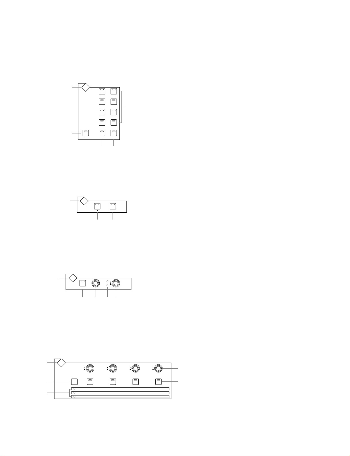
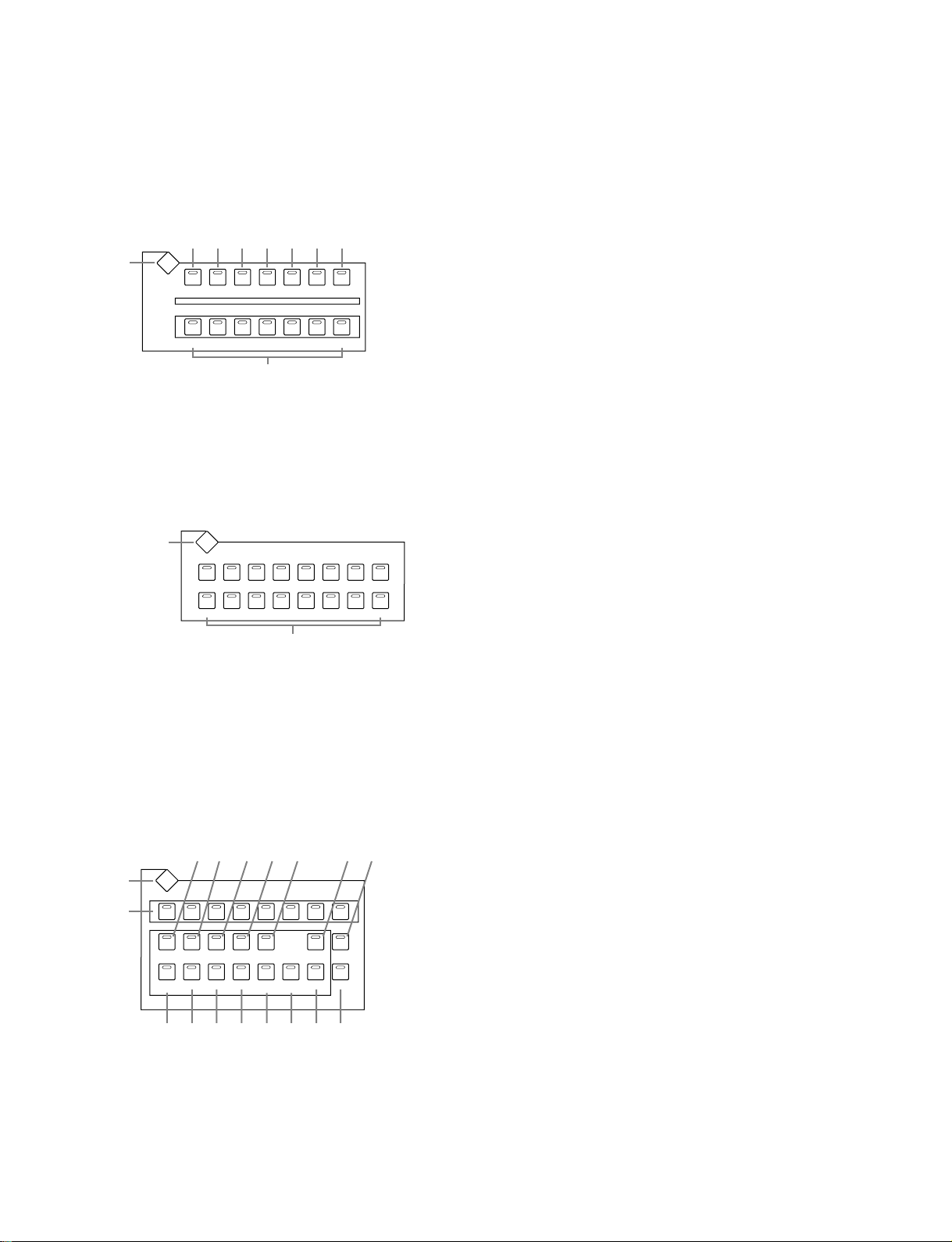
AD Input Section (p. 21)
SmartMedia
CARD Slot (p. 22)
MATRIX SELECT
(p. 22)
AUX SELECT
(p. 22)
FADER MODE
(p. 22)
ENCODER
MODE (p. 22)
EFFECTS/PLUG-INS
(p. 23)
DISPLAY ACCESS (p. 23)
+
48V+48V+48V+48V+48V+48V+48V+48V+48V+48V+48V+48V+48V+48V+48V+48V+48V+48V+48V+48V+48V+48V+48V+48V
ON
OFF
PAD
26dB
26dB
-
60
-
16
-
16
GAIN
GAIN
PEAK
PEAK
SIGNAL
SIGNAL
2
1
OFF
ON
INSERT
INSERT
DISPLAY
DISPLAY
DISPLAY
AUTO
SEL
SOLO
ON
ON
OFF
-
60
-
SIGNAL
OFF
ON
MATRIXSELECT
MATRIX2MATRIX4MATRIX
MATRIX
1
AUXSELECT
AUX10AUX9AUX
ENCODER MODE
PAN
AUX/ MTRX
PAN SEND LEVEL
ASSIGN2ASSIGN
1
AUTO
SEL
SOLO
ON
ON
OFF
26dB
-
60
16
GAIN
PEAK
3
OFF
ON
INSERT
3.3V
CARD
AUX2AUX1AUX3AUX
AUX6AUX5AUX
7
11
FADER
AUTO
SEL
SOLO
ON
26dB
-
16
GAIN
PEAK
SIGNAL
4
INSERT
3
AUX
AUX
FADER MODE
AUX/ MTRX
ASSIGN4ASSIGN
3
INSERTSENDASSIGNOUTPUTINPUT
AUTO
SOLO
ON
OFF
26dB
-
60
-
16
GAIN
PEAK
SIGNAL
5
OFF
ON
INSERT
4
8
12
DISPLAY
AUTO
SEL
SEL
SOLO
ON
ON
ON
ON
OFF
OFF
26dB
-
60
-
60
-
16
-
16
GAIN
PEAK
PEAK
SIGNAL
SIGNAL
6
OFF
OFF
ON
ON
INSERT
INSERT
DISPLAYACCESS
DATA DIO SETUP UTILITY
MIDI REMOTE METER VIEW
PAIR GROUP INPUT
EFFECTS/ PLUG INS
INTERNAL
GRAPHIC
PLUG INS
EFFECTS
EQUALIZERS
1234
5678
AUTO
AUTO
SEL
SEL
SOLO
SOLO
ON
ON
ON
OFF
26dB
26dB
-
60
-
16
GAIN
GAIN
PEAK
SIGNAL
78
OFF
ON
INSERT
OUTPUT
PATCH
PATCH
CHANNEL
INSERTS
AUTO
SEL
SOLO
ON
87654321 910111213 141516 1718192021222324
ON
ON
ON
OFF
OFF
OFF
26dB
26dB
-
60
-
60
-
60
-
16
-
16
GAIN
GAIN
PEAK
PEAK
SIGNAL
SIGNAL
910 21 22 23 24
OFF
OFF
OFF
ON
ON
ON
INSERT
INSERT
AUTO
AUTO
SEL
SEL
SOLO
SOLO
ON
ON
Display Section (p. 24)
ON
ON
ON
ON
OFF
26dB
26dB
-
60
-
16
-
16
GAIN
GAIN
PEAK
PEAK
SIGNAL
SIGNAL
11
12 13 14 15
OFF
ON
INSERT
INSERT
F1F2F
1234
AUTO
AUTO
SEL
SEL
SOLO
SOLO
ON
ON
OFF
OFF
OFF
26dB
26dB
-
60
-
60
-
60
-
16
-
16
GAIN
GAIN
PEAK
PEAK
SIGNAL
SIGNAL
OFF
OFF
OFF
ON
ON
ON
INSERT
INSERT
F
4
3
AUTO
AUTO
SEL
SEL
SOLO
SOLO
ON
ON
SELECTED CHANNEL Section (p. 24)
ON
ON
ON
ON
ON
ON
ON
ON
OFF
OFF
26dB
26dB
26dB
-
60
-
60
-
16
-
16
-
16
PEAK
SIGNAL
INSERT
AUTO
SEL
SOLO
ON
GAIN
GAIN
GAIN
PEAK
PEAK
SIGNAL
SIGNAL
16
17
OFF
OFF
ON
ON
INSERT
INSERT
AUTO
SEL
SOLO
ON
OFF
OFF
26dB
-
60
-
16
GAIN
PEAK
SIGNAL
18 19 20
OFF
ON
INSERT
ROUTING
DISPLAY
STEREOFOLLOWPAN DIRECT
DYNAMICS
DISPLAY
GATEON COMP ON
PAN/ SURROUND
DISPLAY
EQUALIZER
DISPLAY
CHANNEL
COPY
EQON
PASTE
AUTO
AUTO
SEL
SEL
SOLO
SOLO
ON
ON
26dB
-
60
-
16
GAIN
PEAK
SIGNAL
OFF
ON
INSERT
12
34
56
78
R
L
ATT.
AUTO
SEL
SOLO
OFF
26dB
-
60
-
16
GAIN
PEAK
SIGNAL
OFF
ON
INSERT
DISPLAY
DISPLAY
GATE/ COMP
GATE
COMP
L
ODD
FREQUENCY
Q
AUTO
SEL
SOLO
ON
ON
OFF
OFF
OFF
26dB
26dB
-
60
-
60
-
60
-
16
-
16
GAIN
GAIN
PEAK
PEAK
SIGNAL
SIGNAL
OFF
OFF
OFF
ON
ON
ON
INSERT
INSERT
SELECTED CHANNEL
PHASE/ INSERT
INSERTON
AUX/ MATRIX SEND
LEVEL
BANK
ON
AUX1/MATRIX
1
AUX2/MATRIX
AUX
5
AUX
9
RANGE
ATTACK
THRESHOLD HOLD
RATIO
ATTACK
R
EVEN
LINK GRAB EFFECT
LOW
FREQUENCY
Q
GAIN
GAIN
dB
dB
Hz
Hz
kHz
kHz
AUTO
AUTO
AUTO
SEL
SEL
SEL
SOLO
SOLO
SOLO
ON
ON
ON
CH01 CH02 CH03 CH04 CH05 CH06 CH07 CH08 CH09 CH10 CH11 CH12 CH13 CH14 CH15 CH16 CH17 CH18 CH19 CH20 CH21 CH22 CH23 CH24
0
0
10
10
5
5
5
10
0
0
15
5
5
20
10
10
30
15
15
40
20
20
30
30
50
40
40
60
50
50
70
Channel strips (p. 21)
0
0
10
10
5
5
5
5
10
10
0
0
15
15
5
5
20
20
10
10
30
30
15
15
40
40
20
20
30
30
50
50
40
40
60
60
50
50
70
70
0
0
10
10
5
5
5
5
10
10
0
0
15
15
5
5
20
20
10
10
30
30
15
15
40
40
20
20
30
30
50
50
40
40
60
60
50
50
70
70
0
0
10
10
5
5
5
5
5
10
10
10
0
0
15
15
15
5
5
20
20
20
10
10
30
30
30
15
15
40
40
40
20
20
30
30
50
50
50
40
40
60
60
60
50
50
70
70
70
87654321
0
0
10
10
5
5
5
10
0
0
15
5
5
20
10
10
30
15
15
40
20
20
30
30
50
40
40
60
50
50
70
0
0
10
10
5
5
5
5
10
10
0
0
15
15
5
5
20
20
10
10
30
30
15
15
40
40
20
20
30
30
50
50
40
40
60
60
50
50
70
70
0
0
10
10
5
5
5
5
10
10
0
0
15
15
5
5
20
20
10
10
30
30
15
15
40
40
20
20
30
30
50
50
40
40
60
60
50
50
70
70
0
0
10
10
5
5
5
5
5
10
10
10
0
0
15
15
15
5
5
20
20
20
10
10
30
30
30
15
15
40
40
40
20
20
30
30
50
50
50
40
40
60
60
60
50
50
70
70
70
0
0
10
10
5
5
5
10
0
0
15
5
5
20
10
10
30
15
15
40
20
20
30
30
50
40
40
60
50
50
70
0
0
10
10
5
5
5
5
10
10
0
0
15
15
5
5
20
20
10
10
30
30
15
15
40
40
20
20
30
30
50
50
40
40
60
60
50
50
70
70
0
0
10
10
10
5
5
5
5
5
5
10
10
10
0
0
0
15
15
15
5
5
5
20
20
20
10
10
10
30
30
30
15
15
15
40
40
40
20
20
20
30
30
30
50
50
50
40
40
40
60
60
60
50
50
50
70
70
70
9 10111213141516 1718192021222324
CHANNEL (COPY/PASTE) (p. 27)
LAYER (p. 27)
Monitor, Phones &
Talkback Section
(p. 30)
ON
ON
OFF
OFF
010
RELATIVE
REHEARSAL
TALKBACKLEVEL
PHONES
010
010
STUDIO
PHONES
LEVEL
LEVEL
MONITOR
DISPLAY
STUDIO
STEREO
CONTROL
ROOM
AUX11AUX
12
SOLO
SOLOCONTRAST
16
CLEAR
CONTROLROOM
STEREO
MASTERALLCLEAR
2TRD1 2TRA1
2TRD2 2TRA2
2TRD3 STEREO
ASSIGN1ASSIGN
SURROUND
BUS
TOUCH
SENSE
ASSIGN1ASSIGN
EQAUX AUX
ON
SURROUND
MONITOR LEVEL
DIMMER
MONO
SMALL
100
CONTROLROOM LEVEL
TALKB ACK
SLATE
SET
MASTER
TALKBAC K
REC
DEC
INC
MONITOR
Section (p. 31)
TRACK
ARMING (p. 28)
SCENE
MEMORY (p. 28)
2
AUTOMIX (p. 29)
2
USER DEFINED
KEYS (p. 29)
LOCATOR (p. 29)
26dB
26dB
-
60
-
60
-
16
-
16
GAIN
GAIN
PEAK
PEAK
SIGNAL
SIGNAL
OFF
OFF
ON
ON
INSERT
INSERT
DELAY
FB
DISPLAY
MIX
ON
TIME
LEVELONLEVEL
LEVEL
ON
2
AUX
6
AUX
10
DECAY
RELEASETHRESHOLD
FREQUENCY
Q
AUTO
SOLO
0
10
5
5
10
0
15
5
20
10
30
15
40
20
30
50
40
60
50
70
ON
AUX3/MATRIX
3
AUX4/MATRIX
4
AUX
7
AUX
8
AUX
11
AUX
12
GAIN
HIGH
HIGH MIDLOW MID
FREQUENCY
Q
GAIN
GAIN
dB
dB
Hz
Hz
kHz
kHz
LAYER
REMOTE
124
REMOTE
25 48
SEL
ON
REMOTE
49 72
REMOTE
73 96
MASTER
STEREO
AUTO
SEL
ON
0
0
5
5
10
10
15
15
20
20
30
30
40
40
50
50
60
60
70
70
STEREO
0010
SMALL
TRIM
TRACKARMING
DISPLAY
12 45678
3
910 12131415
11
ABCD
TRACKARMING GROUP
SCENE MEMORY
DISPLAY
AUTOMIX
DISPLAY
ENABLE
REC ABORT/
UNDO
SUSPEND WRITE TOUCH LATCH READ TRIM OFF
FADER O N
1
2
3
4
PAN
USER DEFINED KEYS
DISPLAY
12345678
910111213141516
LOCATOR
DISPLAY
LOCATEMEMORY
12345678
PRE POST
IN OUT MTR
AUDITION
RETURN
END QUICK
ONLINE
LOOP
TOZE RO
REW
FF STOP PLAY
DISPLAY HISTORY
BACK FORWARD
SHUTTLE
SCRUB
ENTER
21 22 23 2417 18 2019
STORE RECALL
AUTO-
RETURN
REC
OVERWRIT E
SURROUND
ROLL
BACK
PUNCH
Data Entry & Transport (p. 30)
STEREO (p. 28)
Page 21
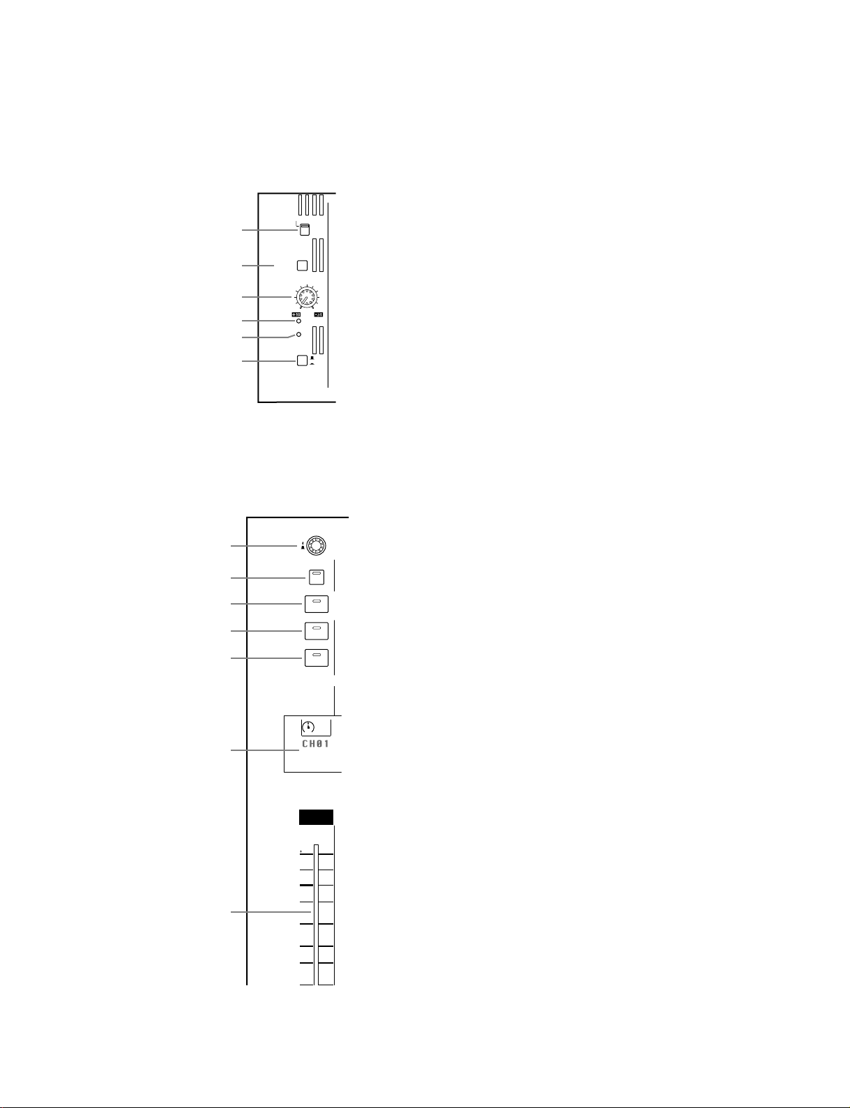
AD Input Section
q
DM2000
+
48V
ON
OFF
Channel strips
q
w
e
r
t
y
w
e
r
t
y
PAD
26dB
q [+48V ON/OFF] switches
w [PAD] switches
-
16
PEAK
SIGNAL
INSERT
-
60
GAIN
1
OFF
ON
AUTO
SEL
SOLO
e [GAIN] controls
r [PEAK] indicators
t [SIGNAL] indicators
y [INSERT ON/OFF] switches
q Encoders
w [AUTO] buttons
ON
1
e [SEL] buttons
r [SOLO] buttons
t [ON] buttons
y Channel strip displays
u Channel faders
u
10
0
5
5
0
10
5
15
20
10
30
15
40
20
30
50
21
Page 22
DM2000
SmartMedia CARD Slot
MATRIX SELECT
3.3V
CARD
q
DISPLAY
MATRIX
AUX SELECT
q
DISPLAY
ENCODER MODE
q
DISPLAY
MATRIX SELECT
MATRIX
1
w
AUX SELECT
AUX
2
AUX
1
AUX
6
AUX
5
AUX
10
AUX
9
w e
ENCODER MODE
AUX /MTRX
PAN
PAN SEND LEVEL
ASSIGN
ASSIGN
1
2
w
MATRIX
2
MATRIX
3
AUX3AUX
AUX
7
AUX
11
ASSIGN
3
AUX
AUX
ASSIGN
4
4
8
12
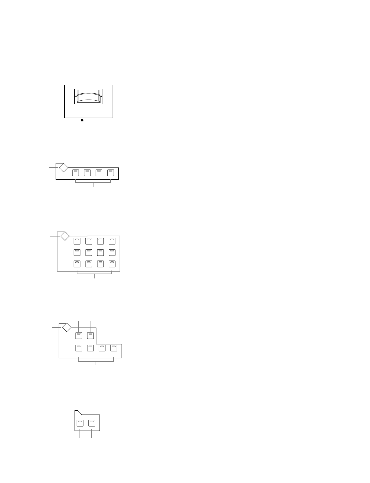
w [MATRIX 1]–[MATRIX 4] buttons
q AUX SELECT [DISPLAY] button
w [AUX 1]–[AUX 12] buttons
q ENCODER MODE [DISPLAY] button
w [PAN] button
e [AUX/MTRX] button
q MATRIX SELECT [DISPLAY] button
4
INSERTSEND ASSIGNOUTPUTINPUT
r [ASSIGN 1]–[ASSIGN 4] buttons
FADER MODE
22
FADER MODE
AUX/ MTRXFADER
q w
r
q [FADER] button
w [AUX/MTRX] button
Page 23
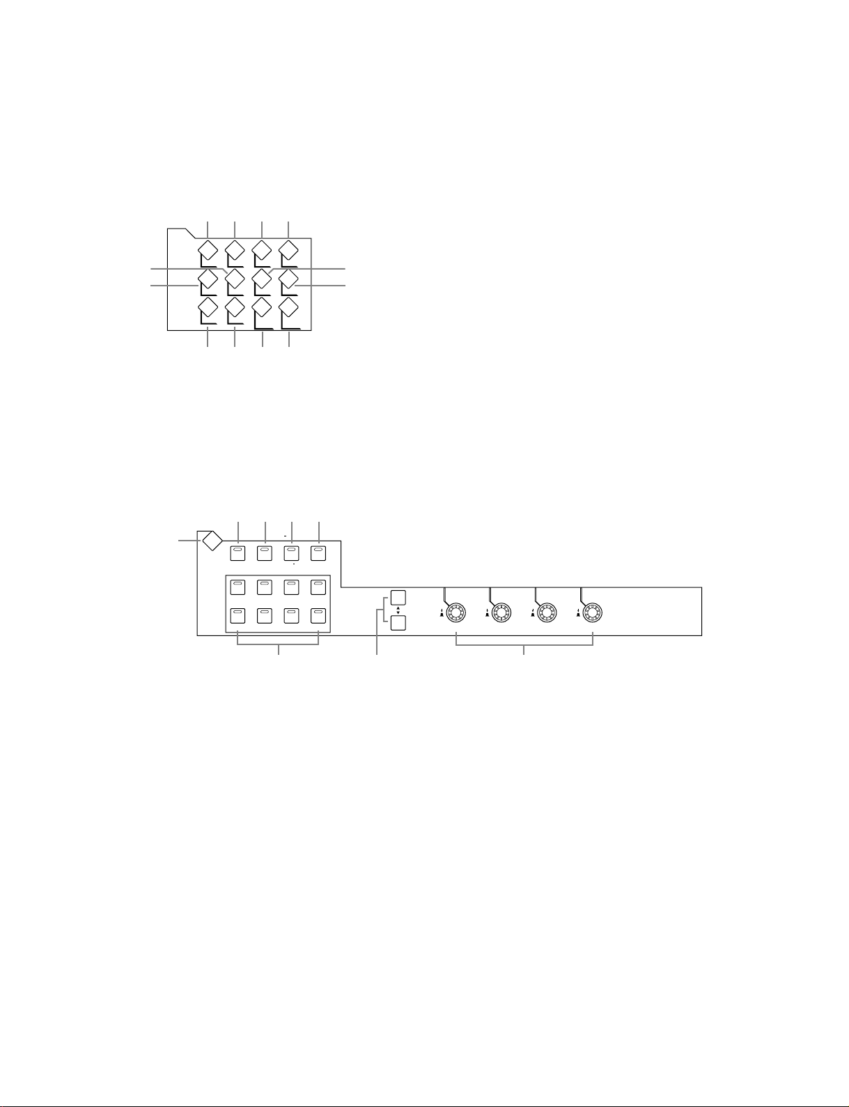
DISPLAY ACCESS
DM2000
q w e r
DISPLAY ACCESS
t
y
DATA DIO SETUP UTILITY
MIDI REMOTE METER VIEW
PAIR GROUP INPUT
o
EFFECTS/PLUG-INS
q
DISPLAY
OUTPUT
PATCH
PATCH
!0
!2!1
w e r t
EFFECTS / PLUG INS
INTERNAL
GRAPHIC
EFFECTS
EQUALIZERS
1234
PLUG INS
CHANNEL
INSERTS
u
i
q [DATA] button
w [DIO] button
e [SETUP] button
r [UTILITY] button
t [REMOTE] button
y [MIDI] button
u [METER] button
i [VIEW] button
o [PAIR] button
!0 [GROUP] button
!1 [INPUT PATCH] button
!2 [OUTPUT PATCH] button
5678
y
u
q EFFECTS/PLUG-INS [DISPLAY] button
w [INTERNAL EFFECTS] button
e [GRAPHIC EQUALIZERS] button
r [PLUG-INS] button
t [CHANNEL INSERTS] button
y EFFECTS/PLUG-INS [1]–[8] buttons
u Parameter Up/Down buttons
i Parameter controls [1]–[4]
1234
i
23
Page 24
DM2000
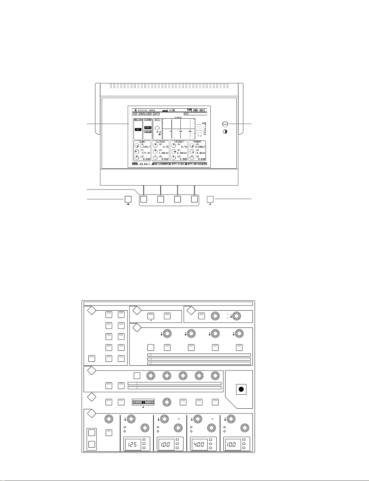
Display Section
q
e
r
q Display
w Contrast control
e [F1]–[F4] buttons
r Left Tab Scroll button
t Right Tab Scroll button
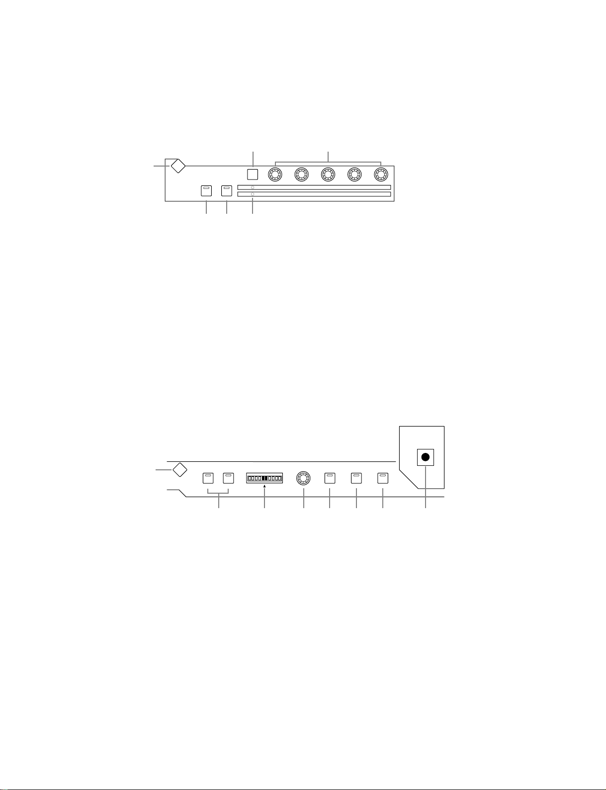
SELECTED CHANNEL Section
w
F
F
1
F
2
4
F
3
t
24
DISPLAY
DISPLAY
DISPLAY
DISPLAY
CHANNEL
COPY
PASTE
ROUTING
12
34
56
78
STEREOFOLLOW PAN DIRECT
DYNAMICS
GATE ON COMP ON
PAN / SURROUND
R
L
EQUALIZER
ATT.
EQ ON
SELECTED CHANNEL
PHASE / INSERT
DISPLAY
INSERT ON
AUX / MATRIX SEND
DISPLAY
GATE / COMP
THRESHOLD HOLD
GATE
COMP
L
ODD
BANK
AUX1/MATRIX
R
EVEN
LEVEL
ON
AUX
AUX
RANGE
RATIO
1
5
9
LOW
FREQUENCY
Q
GAIN
FREQUENCY
Q
dB
Hz
kHz
GAIN
DELAY
DISPLAY
ON
LEVEL
ON
AUX2/MATRIX
2
AUX
AUX
ATTA CK
ATTA CK
LINK GRAB EFFECT
AUX3/MATRIX
6
10
DECAY
RELEASETHRESHOLD
HIGH MIDLOW MID
FREQUENCY
Q
dB
Hz
kHz
GAIN
TIME
LEVEL
ON
AUX
AUX
GAIN
dB
Hz
kHz
FB
MIX
LEVEL
ON
3
AUX4/MATRIX
7
11
4
AUX
8
AUX
12
HIGH
FREQUENCY
Q
GAIN
dB
Hz
kHz
Page 25
ROUTING
DM2000
q
w
PHASE/INSERT
q
DISPLAY
DISPLAY
ROUTING
12
34
56
78
STEREOFOLLOW PAN DIRECT
e r
PHASE / INSERT
INSERT ON
w e
q ROUTING [DISPLAY] button
w [FOLLOW PAN] button
t
e [STEREO] button
r [DIRECT] button
t ROUTING [1]–[8] buttons
q PHASE/INSERT [DISPLAY] button
w Phase [ø] button
e [INSERT ON] button
DELAY
DISPLAY
DELAY
ON
q
w e r t
AUX/MATRIX SEND
DISPLAY
AUX / MATRIX SEND
LEVEL
BANK
ON
AUX1/MATRIX
AUX
AUX
q
w
e
q DELAY [DISPLAY] button
w [ON] button
e [TIME] control
TIME
FB
MIX
r [FB/MIX] indicators
t [FB/MIX] control
q AUX/MATRIX SEND
r
[DISPLAY] button
w [BANK] button
t
e Bank indicators
r [LEVEL] controls
2
LEVEL
ON
AUX3/MATRIX
AUX
AUX
11
7
LEVEL
ON
1
AUX2/MATRIX
5
9
AUX
6
AUX
10
3
LEVEL
ON
AUX4/MATRIX
AUX
8
AUX
12
4
t [ON] buttons
25
Page 26
DM2000
DYNAMICS
w e
DISPLAY
DYNAMICS
GATE ON COMP ON
GATE / COMP
THRESHOLD HOLD
GATE
COMP
RANGE
RATIO
q
r t y
q DYNAMICS [DISPLAY] button
w [GATE/COMP] button
e [THRESHOLD], [RANGE], [ATTACK], [DECAY],
[HOLD] ([THRESHOLD], [RATIO], [ATTACK],
[RELEASE], [GAIN]) controls
r [GATE ON] button
t [COMP ON] button
y [GATE/COMP] indicators
ATTA CK
ATTA CK
RELEASETHRESHOLD
DECAY
GAIN
PAN/SURROUND
DISPLAY
PAN / SURROUND
R
L
L
ODD
EVEN
R
q
w e r t y u i
q PAN/SURROUND [DISPLAY] button
w [L] & [R] buttons
e PAN display
r PAN control
t [LINK] button
y [GRAB] button
u [EFFECT] button
i Joystick
LINK GRAB EFFECT
26
Page 27
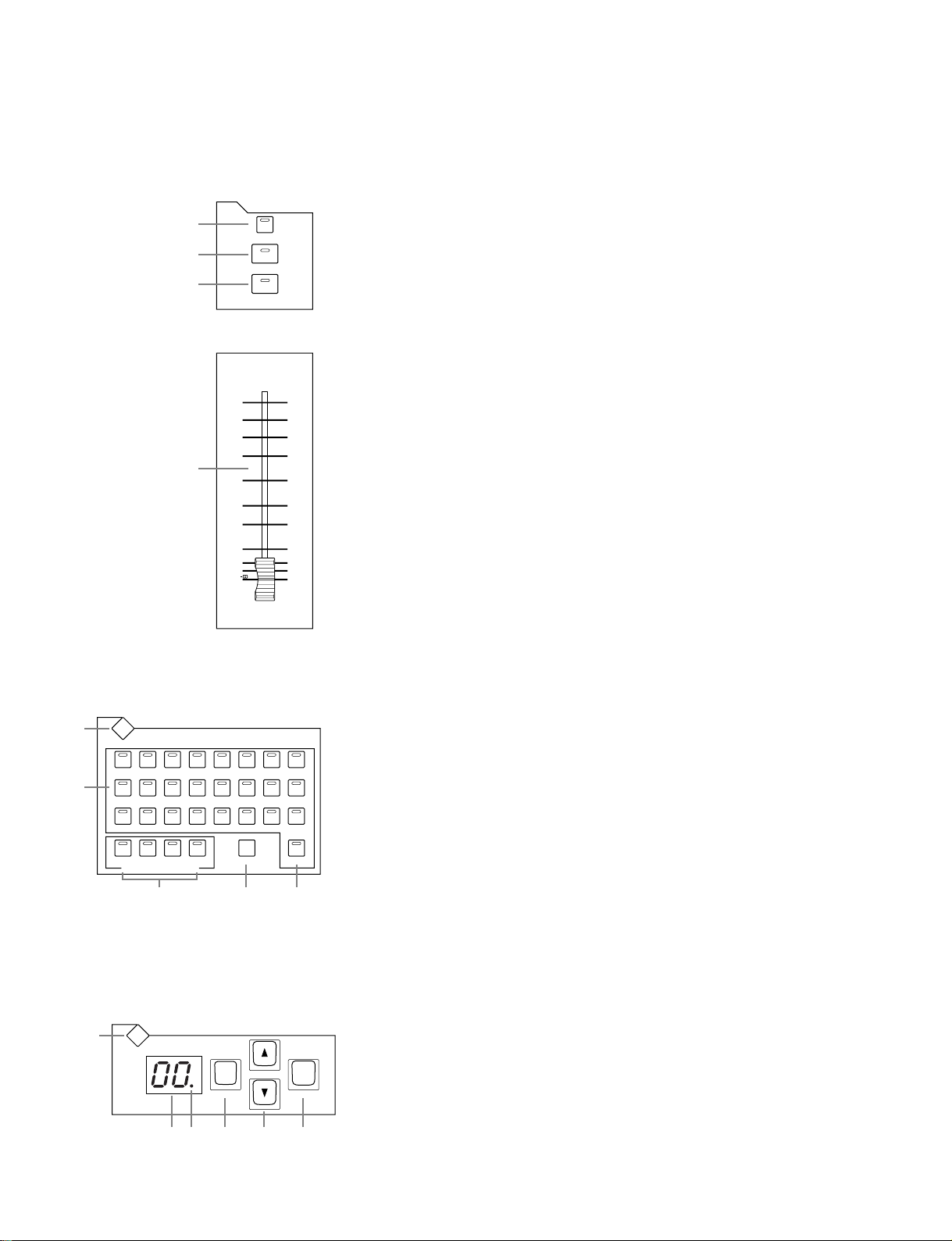
EQUALIZER
ew tr yu
q
EQUALIZER
DISPLAY
CHANNEL
PASTE
COPY
ATT.
EQ ON
FREQUENCY
Q
q EQUALIZER [DISPLAY] button
w [EQ ON] button
e [ATT] control
r [FREQUENCY/Q] indicators
t [FREQUENCY/Q] controls
y EQ [GAIN] controls
u EQ displays
LOW
GAIN
DM2000
FREQUENCY
Q
HIGH
GAIN
dB
Hz
kHz
HIGH MIDLOW MID
FREQUENCY
Q
dB
Hz
kHz
GAIN
FREQUENCY
Q
dB
Hz
kHz
GAIN
dB
Hz
kHz
CHANNEL (COPY/PASTE)
q
w
LAYER
LAYER
REMOTE
124
REMOTE
q e
w
25 48
49 72
73 96
MASTER
REMOTE
REMOTE
CHANNEL
COPY
q [COPY] button
w [PASTE] button
PASTE
1
2
q [1–24], [25–48], [49–72] &
[73–96] buttons
3
4
w [MASTER] button
e [REMOTE 1]–[REMOTE 4] buttons
27
Page 28
DM2000
STEREO
q
w
e
r
0
5
10
15
20
30
40
50
60
70
STEREO
AUTO
SEL
ON
q [AUTO] button
w [SEL] button
e [ON] button
r Fader
TRACK ARMING
q
w
TRACK ARMING
DISPLAY
12 45678
910 12131415
ABCD
TRACK ARMING GROUP
3
11
SCENE MEMORY
q
SCENE MEMORY
DISPLAY
we r yt
STEREO
16
21 22 23 2417 18 2019
MASTERALL CLEAR
tre
STORE RECALL
q TRACK ARMING [DISPLAY] button
w TRACK ARMING [1]–[24] buttons
e TRACK ARMING GROUP
[A]–[D] buttons
r [ALL CLEAR] button
t [MASTER] button
q SCENE MEMORY [DISPLAY] button
w Scene memory display
e Edit indicator
r [STORE] button
t Scene Up/Down buttons
y [RECALL] button
28
Page 29
AUTOMIX
DM2000
w e r t y u i
q
AUTOMIX
DISPLAY
ENABLE
REC ABORT/
AUTO-
SUSPEND WRITE TOUCH LATCH READ TRIM OFF
FADER ON
UNDO
OVERWRITE
PAN
SURROUND
o
USER DEFINED KEYS
q
USER DEFINED KEYS
DISPLAY
12345678
910111213141516
q USER DEFINED KEYS [DISPLAY] button
w USER DEFINED KEYS [1]-[16] buttons
q AUTOMIX [DISPLAY] button
w [ENABLE] button
e [REC] button
RETURN
REC
RELATIVE
TOUCH
SENSE
r [ABORT/UNDO] button
t [AUTO-REC] button
EQAUX AUX
ON
y [RETURN] button
u [RELATIVE] button
i [TOUCH SENSE] button
o [FADER], [ON], [PAN], [SURROUND],
[AUX], [AUX ON] & [EQ] buttons
w
LOCATOR
q
DISPLAY
o
12345678
AUDITION
RETURN
TO ZERO
!0 !1 !2 !3 !4 !5 !6 !7
ty uiwer
LOCATOR
LOCATE MEMORY
IN OUT MTR
PRE POST
ONLINE
END QUICK
LOOP
PUNCH
ROLL
BACK
SET
REHEARSAL
MASTER
q LOCATOR [DISPLAY] button
w [AUDITION] button
e [PRE] button
r [IN] button
t [OUT] button
y [POST] button
u [SET] button
i [MTR] button
o LOCATE MEMORY [1]–[8] buttons
!0 [RETURN TO ZERO] button
!1 [END] button
!2 [ONLINE] button
!3 [LOOP] button
!4 [QUICK PUNCH] button
!5 [ROLL BACK] button
!6 [REHEARSAL] button
!7 [MASTER] button
29
Page 30
DM2000
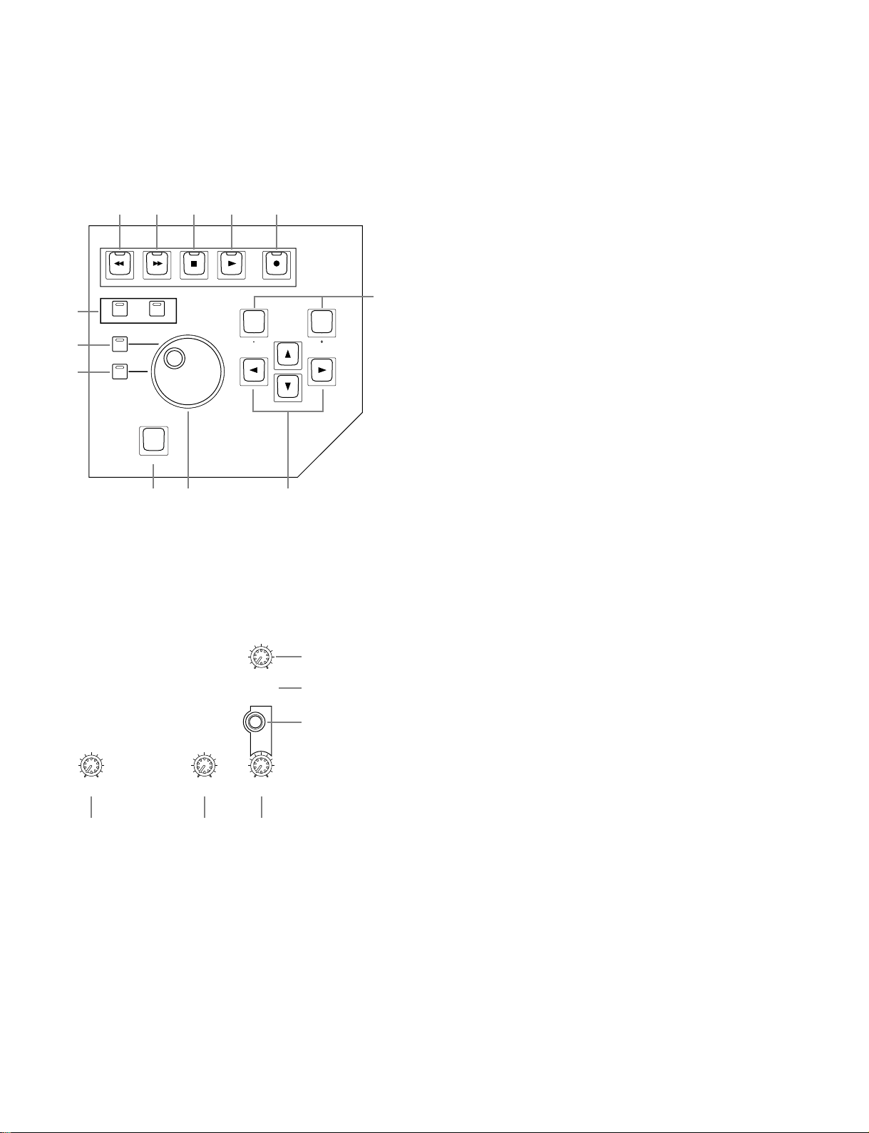
Data Entry & Transport
q w e r t
REW
FF STOP PLAY
DISPLAY HISTORY
y
u
i
BACK FORWARD
SHUTTLE
SCRUB
ENTER
q [REW] button
w [FF] button
REC
e [STOP] button
r [PLAY] button
o
t [REC] button
y DISPLAY HISTORY [BACK]/
DEC
INC
[FORWARD] buttons
u [SHUTTLE] button
i [SCRUB] button
o [–DEC] & [+INC] buttons
!0 [ENTER] button
!1 Parameter wheel
!2 Cursor buttons
!0
!1 !2
Monitor, Phones & Talkback Section
010
TALKBACKLEVEL
PHONES
0010
SMALL
TRIM
010 010
STUDIO
LEVEL
PHONES
LEVEL
q w e
y
t
r
q [SMALL TRIM] control
w [STUDIO LEVEL] control
e [PHONES LEVEL] control
r [PHONES] jack
t T alkback mic
y [TALKBACK LEVEL] control
30
Page 31

MONITOR Section
DM2000
MONITOR
DISPLAY
STUDIO
STEREO
CONTROL
ROOM
AUX 11 AU X12
SOLO
SOLO CONTRAST
CLEAR
CONTROL ROOM
STEREO
2TR D1 2TR A1
2TR D2 2TR A2
2TR D3 STEREO
ASSIGN 1 ASSI GN2
SURROUND
BUS
ASSIGN 1 ASSI GN2
SURROUND
MONITOR LEVEL
DIMMER
MONO
SMALL
100
CONTROL ROOM LEVEL
TALKBACK
SLATE
TALKBACK
STUDIO
q
w
r
MONITOR
DISPLAY
STUDIO
CONTROL
ROOM
AUX 11 AU X12
STEREO
e
t
SOLO
q
SOLO
w
SOLO CONTRAST
e
CLEAR
CONTROL ROOM
CONTROL ROOM
STEREO
q r
2TR D1 2TR A1
w t
2TR D2 2TR A2
e y
2TR D3 STEREO
u i
!0
ASSIGN1ASSIGN
ASSIGN1ASSIGN
SURROUND
2
o
BUS
!1
2
!2
SURROUND
MONITOR LEVEL
!3
!5
MONO
SMALL
DIMMER
!4
!6
100
CONTROL ROOM LEVEL
q MONITOR [DISPLAY] button
w [CONTROL ROOM] button
e [STEREO] button
r [AUX 11] button
t [AUX 12] button
q [SOLO] indicator
w [SOLO CONTRAST] control
e [CLEAR] button
q STEREO [2TR D1] button
w STEREO [2TR D2] button
e STEREO [2TR D3] button
r STEREO [2TR A1] button
t STEREO [2TR A2] button
y [STEREO] button
u STEREO [ASSIGN 1] button
i STEREO [ASSIGN 2] button
o SURROUND [BUS] button
!0 SURROUND [ASSIGN 1] button
!1 SURROUND [ASSIGN 2] button
!2 [SURROUND MONITOR LEVEL]
control
!3 [MONO] button
!4 [DIMMER] button
!5 [SMALL] button
!6 [CONTROL ROOM LEVEL]
control
TALKBACK
TALKBACK
q
SLATE
w
TALKBACK
q [SLATE] button
w [ TALKBACK] button
31
Page 32

32
Rear Panel
DM2000
Analog Master I/O Section (p. 33)
OMNI OUT Section (p.33)
Power Section (p. 34)
AD Input Section (p. 33)
Digital I/O & Control Section (p. 34)
SLOT Section (p. 34)
Page 33

AD Input Section
q
q [INPUT A & B (BAL)] connectors
w [INSERT IN & OUT +4dB (BAL)] connectors
w
Analog Master I/O Section
DM2000
wq
y u
q [STUDIO MONITOR OUT +4 dB (BAL)] jacks
w [STEREO OUT +4 dB (BAL)] connectors
e [SMALL CONTROL ROOM MONITOR OUT
+4 dB (BAL)] connectors
r [LARGE CONTROL ROOM MONITOR OUT
+4 dB (BAL)] connectors
t [2TR IN ANALOG 1 +4 dB (BAL)] jacks
y [STEREO OUT –10 dBV (UNBAL)] connectors
u [2TR IN ANALOG 2 –10 dBV (UNBAL)] connectors
te r
OMNI OUT Section
q
q [OMNI OUT +4dB (BAL)] jacks
33
Page 34

DM2000
Digital I/O & Control Section
q w e r t y u i o !1 !2
!4 !5 !6 !8!7
q [KEYBOARD] connector
w [SMPTE TIME CODE INPUT] connector
e [MTC TIME CODE INPUT] connector
r [USB TO HOST] port
t [SERIAL TO HOST] port
y [WORD CLOCK OUT 2] connector
u [WORD CLOCK OUT 1] connector
i [WORD CLOCK 75Ω ON/OFF] termination switch
o [WORD CLOCK IN] connector
!0 [2TR OUT DIGITAL COAXIAL 3] connector
!1 [2TR OUT DIGITAL AES/EBU 1 & 2] connectors
!2 [2TR IN DIGITAL COAXIAL 3] connector
!3 [2TR IN DIGITAL AES/EBU 1 & 2] connectors
!4 [METER] port
!5 [CONTROL] port
!6 [REMOTE] port
!7 [MIDI IN, OUT & THRU] ports
!8 [CASCADE IN & OUT] ports
!3!0
Power Section
q
w
e
SLOT Section
q [POWER ON/OFF] switch
w Grounding screw
e [AC IN] connector
r Cooling fan
r
q
q [SLOT 1]–[SLOT 6]
34
Page 35

MB2000
Controls
DM2000
y
t
r
e
OVER
TIME CODE
0
CLOCK
BEAT
MEASURE
PEAK
HOLD
POST FADER
PRE EQ PRE FADER
OUTPUTMETERING POSITION
72
STEREO
LR
49 96
148
!0
o
i
LAMP
DIMMER
HMS F
ROOM
CONTROL
8
6
4
2
18
10
12
3
1
2
REMOTE
REMOTE
REMOTE
124
49 72
25 48
56
303642
14
24
48
4
REMOTE
73 96
MASTER
3
6
9
0
18
15
12
36
48
30
24
OVER
q Channel indicators
w [INPUT METERING POSITION] button
& indicators
e [OUTPUT METERING POSITION] button
& indicators
21
93
45
21
69
r [PEAK HOLD] button
t [LAYER] buttons
y [TIMECODE] counter
u Meters
i [STEREO] meters
o [CONTROL ROOM] button
41
89 90 91 92 93 94 95 96
3
6
9
0
18
15
12
36
48
30
24
OVER
!0 [LAMP DIMMER] knob
w
q
POST FADER
PRE FADER
PRE EQ
INPUT METERINGPOSITION
u
21
10
81 82 83 84 85 86 87 88
3
6
9
0
18
15
12
36
48
30
24
OVER
8BUS 7BUS 5
32 33 34 35 36 37 38 39 4031 42 43 44 45 46 47 48
BUS
62 63 64 65 67 68 69 70 7166 72 73 74 75 76 77 78 79 80 81 82 83 84 85 86 87 88 89 9 0 91 92 93 94 95 96
61
10 25 26 27 28 29 30 32 33 34 35 36 37 38 39 4031 42 43 44 45 46 47 4841
76 77 78 79 80
BUS 4BUS 3BUS2BUS1 BUS 6 AUX 12 MATRIX 1 MATRIX 2 MATRIX 3 MATRIX4AUX 11AUX 10AUX 9AUX 8AUX 7AUX 6AUX5AUX4AUX 3AUX 2AUX1
51 52 53 54 55 56 57 58 59 60 61 62 63 64 65 67 68 69 70 7166 72
75
234567891 12 13 14 15 16 17 18 19 2 011 22 23 24
74
73
25 26 27 28 29 30
49 50
234567891 12 1314 1516 1718 192011 22 23 24
49 50 51 52 53 54 55 56 57 58 59 60
3
9
6
0
18
15
12
36
48
30
24
OVER
35
Page 36

DM2000
<
Top View
>
<
Rear View
>
JK2
BRG DSP
CPU
OPT
DA1
DA1
JK1
JK1
Power Supply Unit
CIRCUIT BOARD LAYOUT
DM2000
Bottom Assembly
Power Supply Unit
<
Top View
>
BRG
JK1
CPU
DSP
OPT
36
Page 37

Inside the shield box
DM2000
Shield Box
Shield Box Cover
SW
<
Top View
Power Supply Unit
>
BRG
DSP
OPT
JK2
37
Page 38

DM2000
Rear Assembly U
<
Top View
ANI
#1
ANI
ANI
#3
#2
ANI
#4
<
Rear View
ANI
>
#5
>
ANI
#6
AD
#1
ANI#7ANI
ANI
#8
#9
ANI
#10
ANI
#11
ANI
#12
ANI
#13
ANI
#14
AD
#2
ANI
#15
ANI
ANI
ANI
#16
#18
ANI
#17
#19
ANI
ANI
#20
#21
ANI
#22
2TRI
ANI
#23
LRG
ANI
#24
DA2
SML
PHN
STD
ST
38
<
Top View
PHN
STD
>
ST
LRG
AD #1
ANI
ANI
ANI
ANI
ANI
ANI
ANI
ANI
ANI
ANI
ANI
ANI
#24
ANI
#23
ANI
#22
#21
ANI
#20
#19
ANI
#18
#17
ANI
#16
AD #2
#15
ANI
#14
#13
ANI
#12
#11
ANI
#10
#9
ANI
#8
#7
ANI
#6
DA2
#5
ANI
#4
#3
#1
ANI
#2
2TRISML
Page 39

Control Panel Assembly
<
Bottom View
>
DM2000
PN2 (2/2)
PN4 (2/2)
<
Bottom View
>
PN3
PN4 (1/2)
LCD Assembly
PN2 (1/2)
SUB
FD2
Display Tube B (1/2) Display Tube B (2/2) Display Tube A
FD1
PN2 (2/2)
DS
PN4 (2/2)
PN3
PN4 (1/2)
PN2 (1/2)
LCD Assembly
PN1
Display Tube B (1/2) Display Tube B (2/2) Display Tube A
39
Page 40

DM2000
LCD Assembly
<
Bottom View
>
LCD
<
LCDCOM (CNT)
MB2000
<
Rear View
Bottom View
>
>
LCDCOM (INV)
PN1 PN2
40
Front View
<
>
DC
Page 41

DISASSEMBLY PROCEDURE
Note: Take care not to trap your fingers.
After replacing the circuit board or fader of FD1 or
FD2, please initialize them. (See page 187.)
Disassembling the DM2000
1. Removing the SP2000
(Time required: About 5 minutes)
1-1. If the SP2000 is attached to the DM2000, remove
the twelve (12) screws marked [A], and then both
sides must be removed. (Fig.1)
DM2000
SP2000
(Side pad)
DM2000
[A]: Bind Head Screw 4.0X16 MFZN2BL (EG340110)
2. Removing the MB2000
(Time required: About 5 minutes)
2-1. Loosen the four (4) screws marked [B]. The MB2000
can then be removed from the DM2000. (Photo.1,2)
Meter angle L, R
[B]: Bind Head Screw A4.0X12 MFZN2BL (VP156900)
Photo.1
3. Control Panel Assembly
(Time required: About 10 minutes)
3-1. Remove the SP2000. (See procedure 1.)
3-2. Remove the MB2000. (See procedure 2.)
3-3. Remove the twenty (20) screws marked [60A], the
eight (8) screws marked [60B] and the seven (7)
screws marked [60C]. (Fig.2)
3-4. Hold the LCD assembly part, and lift the control panel
assembly. And then, fasten them by the tw o (2) front
stays. (Photo.3)
When assembling the control panel assembly
with the side panel, put the screws of the
round screw hole of the side panel in place
first, then the screws of the elliptic screw hole.
SP2000
(MB side pad)
Fig.1
MB2000
[B]
DM2000
[A]
Photo.2
41
Page 42

DM2000
4. Rear Assembly U
(Time required: About 15 minutes)
4-1. Remove the SP2000. (See procedure 1.)
4-2. Remove the MB2000. (See procedure 2.)
4-3. Fasten the control panel assembly. (See procedure 3.)
4-4. Remove the two (2) screws marked [60D] and the
seven (7) screws marked [60E]. (Fig.2)
4-5. Lift the rear assembly U from the rear side and fasten
them by the two (2) rear stays . (There are two ways
of using the rear stays shown in the photo 4 or 5.)
Photo.3
<Left side view>
Side panel L
Control panel assembly
Front stay
<Rear view>
[60D]
<Top view>
[60A]
Photo.4
Rear assembly U
Rear stay
[60E] x 7
Rear assembly U
[60C] x 7
Control panel assembly
Photo.5
<Right side view>
[60D]
Side panel R
42
[60A]
<Front view>
[60B] x 8
Bottom assembly
[60]: Bind Head Tapping Screw-B A4.0X8 MFZN2BL (VC688800)
Fig.2
Page 43

Bottom Assembly
5. CPU Circuit Board
(Time required: About 15 minutes)
5-1. Remove the SP2000. (See procedure 1.)
5-2. Remove the MB2000. (See procedure 2.)
5-3. Fasten the control panel assemb ly. (See procedure 3.)
5-4. Remove the five (5) screws marked [335]. The CPU
circuit board can then be removed. (Fig.4)
6. Replacing the Lithium Battery
(Time required: About 15 minutes)
6-1. Remove the SP2000. (See procedure 1.)
6-2. Remove the MB2000. (See procedure 2.)
6-3. Fasten the control panel assemb ly. (See procedure 3.)
6-4. You can replace the lithium battery from the CPU
circuit board. (Fig.4)
The lithium battery is not part of the CPU circuit
board. When you replace the CPU circuit
board, you should remove the lithium battery
from the board, and install in the holder on
the new circuit board.
DM2000
7. DSP Circuit Board
(Time required: About 25 minutes)
7-1. Remove the SP2000. (See procedure 1.)
7-2. Remove the MB2000. (See procedure 2.)
7-3. Fasten the control panel assemb ly. (See procedure 3.)
7-4. Fasten the rear assembly U. (See procedure 4.)
7-5. Remove the CPU circuit board. (See procedure 5.)
7-6. Remove the sev en (7) screws marked [310] and the
five (5) hexagonal spacers. The DSP circuit board
can then be removed. (Fig.3)
8. BRG Circuit Board
(Time required: About 20 minutes)
8-1. Remove the SP2000. (See procedure 1.)
8-2. Remove the MB2000. (See procedure 2.)
8-3. Fasten the control panel assemb ly. (See procedure 3.)
8-4. Fasten the rear assembly U. (See procedure 4.)
8-5. Remove the six (6) screws marked [290A]. The BRG
circuit board can then be removed. (Fig.3)
9. Power Supply Unit
(Time required: About 20 minutes)
9-1. Remove the SP2000. (See procedure 1.)
9-2. Remove the MB2000. (See procedure 2.)
9-3. Fasten the control panel assemb ly. (See procedure 3.)
9-4. Fasten the rear assembly U. (See procedure 4.)
9-5. Remove the eight (8) screws marked [255]. The
power supply unit can then be removed. (Fig.3)
Noise will be generated if a bundle of cables for
VOLUME is routed over the power supply unit,
so make sure it is routed as shown in Photo 6.
Never route as shown in Photo 7. (Photo.6, 7)
43
Page 44

DM2000
<OK> <NG>
Photo.6 Photo.7
10. OPT Circuit Board
(Time required: About 20 minutes)
10-1. Remove the SP2000. (See procedure 1.)
10-2. Remove the MB2000. (See procedure 2.)
10-3. Fasten the control panel assembly. (See procedure 3.)
10-4. Fasten the rear assembly U. (See procedure 4.)
10-5. Remove the six (6) screws marked [270A]. The OPT
circuit board can then be removed. (Fig.3)
11. DA1 and JK1 Circuit Boards
(Time required: About 25 minutes each)
11-1. Remove the SP2000. (See procedure 1.)
11-2. Remove the MB2000. (See procedure 2.)
11-3. Fasten the control panel assembly. (See procedure 3.)
11-4. Fasten the rear assembly U. (See procedure 4.)
11-5. Remove the six (6) screws marked [235], the thirteen
(13) screws marked [370], the six (6) screws marked
[380] and the four (4) screws marked [400]. The
P.C.B. holder and the duct can then be removed with
the DA1 and JK1 circuit boards. (Fig.4, 5)
11-6. DA1 Circuit Board:
Remove the three (3) screws marked [240]. The DA1
circuit board can then be removed from P.C.B. holder .
(Fig.5)
11-7. JK1 Circuit Board:
Remove the D A1 circuit board. (See procedure 11-6.)
Remove the three (3) screws marked [365]. The JK1
circuit board can then be removed from P.C.B. holder .
(Fig.4)
12. JK2 Circuit Board
(Time required: About 25 minutes)
12-1. Remove the SP2000. (See procedure 1.)
12-2. Remove the MB2000. (See procedure 2.)
12-3. Fasten the control panel assembly. (See procedure 3.)
12-4. Fasten the rear assembly U. (See procedure 4.)
12-5. Remove the P.C.B. holder and the duct with the DA1
and JK1 circuit boards. (See procedure 11-5.)
12-6. Remove the three (3) screws marked [345], the two
(2) screws marked [350A], the two (2) screws marked
[355], the two (2) screws marked [C], the two (2)
screws marked [D], the two (2) screws marked [E]
and the two (2) screws marked [F]. The JK2 circuit
board can then be removed. (Fig.3, 5)
44
Page 45

13. DC Fan Motor
(Time required: About 20 minutes)
13-1. Remove the SP2000. (See procedure 1.)
13-2. Remove the MB2000. (See procedure 2.)
13-3. Fasten the control panel assembly. (See procedure 3.)
13-4. Fasten the rear assembly U. (See procedure 4.)
13-5. Remove the four (4) screws marked [130]. The DC
fan motor , the tw o (2) fan guides, the fan guard and
the two (2) toothed lock washers can then be
removed. (Fig.3)
<Top view>
[255] x 8
Power supply unit
[290A] x 6
DM2000
Spacer
[310] x 7
BRG DSP
[430] [220A]
Fan guide
JK2
Shield box
[130] x 2
[130] x 2
Fan guard
[130]: Pan Head Screw SP 4.0X20 MFZN2BL (VB671600)
[220A]:Bind Head Tapping Screw-S 4.0X8 MFZN2BL (VI693100)
[255]: Bind Head Tapping Screw-B 3.0X8 MFZN2BL (EP600190)
[270A]:Bind Head Screw 4.0X8 SP MFZN2Y (VZ538000)
[290A]:Bind Head Tapping Screw-B 3.0X8 MFZN2BL (EP600190)
[310]: Bind Head Tapping Screw-B 3.0X8 MFZN2BL (EP600190)
[345]: Bind Head Tapping Screw-B 3.0X8 MFZN2BL (EP600190)
[430]: Bind Head Tapping Screw-B 3.0X8 MFZN2BL (EP600190)
DC fan motor
Fig.3
14. A C Inlet Assembly and SW Circuit Boar d
(Time required: About 25 minutes each)
14-1. Remove the SP2000. (See procedure 1.)
14-2. Remove the MB2000. (See procedure 2.)
14-3. Fasten the control panel assembly. (See procedure 3.)
14-4. Fasten the rear assembly U. (See procedure 4.)
14-5. Remove the screw marked [220A], the two (2) screws
marked [225] and the two (2) screws marked [430].
The shield box can then be removed with the A C inlet
assembly and the SW circuit board. (Fig.3, 5, 6)
14-6. Remove the six (6) screws marked [205A]. The shield
box cov er can then be removed from the shield box. (Fig.6)
OPT
[270A]
[345]
45
Page 46

DM2000
14-7. AC Inlet Assembly:
Remove the screw marked [205B] and the cord
holder. The AC inlet assembly can then be removed
from the shield box. (Fig.6)
14-8. SW Circuit Board:
Remove the power s witch knob , the three (3) screws
marked [205C] and the two (2) screws marked
[210A]. The SW circuit board can then be removed
from the shield box. (Fig.5, 6)
Rear Assembly U
15. PC Support
(Time required: About 15 minutes)
15-1. Remove the SP2000. (See procedure 1.)
15-2. Remove the MB2000. (See procedure 2.)
15-3. Fasten the control panel assembly. (See procedure 3.)
15-4. Remove the sixteen (16) screws marked [190], the
twenty-four (24) nuts marked [200A], the five (5) n uts
marked [210B] and the twenty-eight (28) knobs
marked [220B]. The PC suppor t can then be
removed from the rear assembly U. (Fig.7)
<Top view>
JK1
Duct P.C.B. holder
[335]: Bind Head Screw 3.0X8 MFZN2BL (VB659000)
[365]: Bind Head Tapping Screw-B 3.0X8 MFZN2BL (EP600190)
[400]: Bind Head Tapping Screw-B 3.0X8 MFZN2BL (EP600190)
[365] x 3[400] x 4
Fig.4
CPU
Lithium Battery
Battery VN103500
VN103600(Battery holder for VN103500)
Notice for back-up battery removal
Push the battery as shown in figure,
then the battery will pop up.
Druk de batterij naar beneden zoals
aangeven in de tekening de batterij
springt dan naar voren.
[335] x 5
Battery
Battery holder
46
Page 47

<Top view>
DM2000
DA1
<Rear view>
[225]
Power switch knob
<Top view>
[240]
Power switch escutcheon
[380][380]
[370] [235] x 6
[D] [E] [F][355]
[C]
[350A]
[370]
P.C.B.holder
Rear panel L
[225]: Bonding Tapping Screw-B 3.0X8 MFZN2BL (VN413300)
[235]: Bonding Tapping Screw-B 3.0X8 MFZN2BL (VN413300)
[240]: Bind Head Tapping Screw-B 3.0X8 MFZN2BL (EP600190)
[350A]:Bonding Tapping Screw-B 3.0X8 MFZN2BL (VN413300)
[355]: Hex. Locking Screw JFS-2.6S-BIW (VS604900)
[370]: Bonding Tapping Screw-B 3.0X8 MFZN2BL (VN413300)
[380]: Bonding Screw 3.0X8 MFZN2BL (VP157800)
Fig.5
[205A]
[205C]
Shield box
SW
Shield box cover
[205C]
Ferrite core
Cord holder
[205C]
[205A]
[205]: Bind Head Tapping Screw-B 3.0X8 MFZN2BL (EP600190)
[210A]:Bind Head Screw 3.0X8 MFZN2BL (VB659000)
Fig.6
[210A]
AC inlet assembly
[205B]
AC inlet
47
Page 48

DM2000
16. ANI Circuit Board
(Time required: About 20 minutes)
16-1. Remove the SP2000. (See procedure 1.)
16-2. Remove the MB2000. (See procedure 2.)
16-3. Fasten the control panel assembly. (See procedure 3.)
16-4. Remove the PC support. (See procedure 15.)
16-5. Remove the four (4) screws marked [160A] and
disconnect the connector from the AD circuit board.
The ANI circuit board can then be removed. (Fig.7)
There is a total of twenty-four (24) ANI circuit
boards, and they can all be removed in this way .
17.
2TRI, LRG, SML, ST , STD, PHN Circuit Boards
(Time required: About 20 minutes each)
17-1. Remove the SP2000. (See procedure 1.)
17-2. Remove the MB2000. (See procedure 2.)
17-3. Fasten the control panel assembly. (See procedure 3.)
17-4. Remove the PC support. (See procedure 15.)
17-5. 2TRI Circuit Board:
Remove the two (2) screws marked [160B] and
disconnect the connector from the DA2 circuit board.
The 2TRI circuit board can then be removed. (Fig.7)
17-6. LRG Circuit Board:
Remove the four (4) screws marked [160C] and
disconnect the connector from the DA2 circuit board.
The LRG circuit board can then be removed. (Fig.7)
17-7. SML Circuit Board:
Remove the four (4) screws marked [160D] and
disconnect the connector from the DA2 circuit board.
The SML circuit board can then be removed. (Fig.7)
17-8. ST Circuit Board:
Remove the four (4) screws marked [160E] and
disconnect the connector from the DA2 circuit board.
The ST circuit board can then be removed. (Fig.7)
17-9. STD Circuit Board:
Remove the two (2) screws marked [160F] and
disconnect the connector from the DA2 circuit board.
The STD circuit board can then be removed. (Fig.7)
17-10. PHN Circuit Board:
Remove the two (2) screws marked [170] and
disconnect the connector from the DA2 circuit board.
The PHN circuit board can then be removed. (Fig.7)
18. AD Circuit Board
(Time required: About 25 minutes)
18-1. Remove the SP2000. (See procedure 1.)
18-2. Remove the MB2000. (See procedure 2.)
18-3. Fasten the control panel assembly. (See procedure 3.)
18-4. Remove the PC support. (See procedure 15.)
18-5. Remove the twelve (12) ANI circuit boards.
(See procedure 16.)
18-6. Remove the eight (8) screws marked [80A]. The AD
circuit board can then be removed. (Fig.8)
There is a total of two (2) AD circuit boards,
and they can all be removed in this way.
48
Page 49

19. DA2 Circuit Board
(Time required: About 25 minutes)
19-1. Remove the SP2000. (See procedure 1.)
19-2. Remove the MB2000. (See procedure 2.)
19-3. Fasten the control panel assembly. (See procedure 3.)
19-4. Remove the PC support. (See procedure 15.)
19-5. Remove the 2TRI, LRG, SML, ST, STD and PHN
circuit boards. (See procedure 17.)
19-6. Remove the eight (8) screws marked [80B]. The D A2
circuit board can then be removed. (Fig.8)
DM2000
<Top view>
[200A] x 24
ANI
x 24
<Rear view>
[170]
[190] x 16
[160F]
[220B] x 28
AD
[160E] [160C]
[160D] [160B]
AD
2TRI
PC support
LRG
[210B] x 5
DA2
SML
ST
[160]: Bonding Tapping Screw-B 3.0X8 MFZN2BL (VN413300)
[170]: Bind Head Screw A4.0X8 MFZN2BL (VP156800)
[190]: Bind Head Tapping Screw-B A4.0X8 MFZN2BL (VC688800)
[200A]:Hexagonal Nut 7.0 11X2 MFZN2BL (VR991600)
[210B]:Hexagonal Nut 9.0 11X2 MFZN2BL (VJ388000)
Fig.7
PHN
STD
[160A] x 96
<Top view>
Rear panel U
AD AD DA2
[80A] x 8
[80A] x 8 [80B] x 8
[80]: Bind Head Tapping Screw-B 3.0X8 MFZN2BL (EP600190)
Fig.8
49
Page 50

DM2000
Control Panel Assembly
When removing the circuit board, if it is har d to handle
while the control panel assembly is fixed slantwise
at the front stay, open it widely at 180° for the work.
20. SUB Circuit Board
(Time required: About 15 minutes)
20-1. Remove the SP2000. (See procedure 1.)
20-2. Remove the MB2000. (See procedure 2.)
20-3. Fasten the control panel assembly. (See procedure 3.)
20-4. Remove the ten (10) screws marked [200B]. The
SUB circuit board can then be removed. (Fig.10)
21. PN1 Circuit Board
(Time required: About 20 minutes)
21-1. Remove the SP2000. (See procedure 1.)
21-2. Remove the MB2000. (See procedure 2.)
21-3. Remove the four (4) encoder knobs marked [330A]
and the sixteen (16) encoder knobs marked [338A]
from the control panel side. (Fig.9)
21-4. Fasten the control panel assembly. (See procedure 3.)
21-5. Remove the SUB circuit board. (See procedure 20.)
21-6. Remove the twenty-four (24) screws marked [150A].
The PN1 circuit board can then be removed. (Fig.11)
22. PN2 (1/2) Circuit Board
(Time required: About 20 minutes)
22-1. Remove the SP2000. (See procedure 1.)
22-2. Remove the MB2000. (See procedure 2.)
22-3. Remove the four (4) encoder knobs marked [330B],
the five (5) encoder knobs marked [332], the four (4)
encoder knobs marked [334], the eight (8) encoder
knobs marked [336] and the eight (8) encoder knobs
marked [338B] from the control panel side. (Fig.9)
22-4. Fasten the control panel assembly. (See procedure 3.)
22-5. Remove the twenty-one (21) screws marked [150B].
The PN2 (1/2) circuit board can then be removed.
(Fig.11)
23. PN2 (2/2) Circuit Board
(Time required: About 15 minutes)
23-1. Remove the SP2000. (See procedure 1.)
23-2. Remove the MB2000. (See procedure 2.)
23-3. Fasten the control panel assembly. (See procedure 3.)
23-4. Remove the four (4) screws marked [150C]. The PN2
(2/2) circuit board can then be removed. (Fig.11)
24. PN3 Circuit Board
(Time required: About 20 minutes)
24-1. Remove the SP2000. (See procedure 1.)
24-2. Remove the MB2000. (See procedure 2.)
24-3. Remove the knob marked [340] and the two (2)
knobs marked [350B] from the control panel side.
(Fig.9)
24-4. Fasten the control panel assembly. (See procedure 3.)
24-5. Remove the eighteen (18) screws marked [150D].
The PN3 circuit board can then be removed. (Fig.11)
50
Page 51

25. PN4 Circuit Board
(Time required: About 15 minutes)
25-1. Remove the SP2000. (See procedure 1.)
25-2. Remove the MB2000. (See procedure 2.)
25-3. Remove the knob wheel and the hexagonal nut from
the control panel side. (Fig.9, Photo.8)
25-4. Fasten the control panel assembly. (See procedure 3.)
25-5. Remove the eight (8) screws marked [150E]. The
PN4 circuit board can then be removed. (Fig.11)
26. FD1 Circuit Board
(Time required: About 20 minutes)
26-1. Remove the SP2000. (See procedure 1.)
26-2. Remove the MB2000. (See procedure 2.)
26-3. Remove the sixteen (16) fader knobs marked [320A]
from the control panel side. (Fig.9)
26-4. Fasten the control panel assembly. (See procedure 3.)
26-5. Remove the sixteen (16) scre ws marked [230A]. The
FD1 circuit board can then be removed. (Fig.10)
DM2000
27. FD2 Circuit Board
(Time required: About 20 minutes)
27-1. Remove the SP2000. (See procedure 1.)
27-2. Remove the MB2000. (See procedure 2.)
27-3. Remove the nine (9) fader knobs marked [320B] from
the control panel side. (Fig.9)
27-4. Fasten the control panel assembly. (See procedure 3.)
27-5. Remove the ten (10) screws marked [230B]. The
FD2 circuit board can then be removed. (Fig.10)
28. DS Circuit Board
(Time required: About 15 minutes)
28-1. Remove the SP2000. (See procedure 1.)
28-2. Remove the MB2000. (See procedure 2.)
28-3. Fasten the control panel assembly. (See procedure 3.)
28-4. Remove the two (2) screws marked [270B]. The DS
circuit board can then be removed with the smart
media escutcheon and the smart media angle
bracket. (Fig.10)
28-5. Remove the two (2) screws marked [265]. The smart
media escutcheon and the smart media angle
bracket can then be removed from the DS circuit
board. (Fig.10)
29. Display Tube A and B (1/2, 2/2)
(Time required: About 15 minutes each)
29-1. Remove the SP2000. (See procedure 1.)
29-2. Remove the MB2000. (See procedure 2.)
29-3. Fasten the control panel assembly. (See procedure 3.)
29-4. Display Tube A:
Remove the four (4) screws marked [180A]. The
display tube A can then be removed. (Fig.11)
29-5. Display Tube B (1/2):
Remove the four (4) screws marked [180B]. The
display tube B (1/2) can then be removed. (Fig.11)
51
Page 52

DM2000
29-6. Display Tube B (2/2):
Remove the four (4) screws marked [180C]. The
display tube B (2/2) can then be removed. (Fig.11)
30. LCD Assembly
(Time required: About 5 minutes)
30-1. Remove the eight (8) screws marked [290B] from
the control panel side. The LCD assembly can then
be removed. (Fig.9)
Be careful no to scratch the control panel during
installation.
Hexagonal nut
Control panel
[338A] x 16
[320A] x 16
<Top view>
Control panel
LCD assembly
Photo.8
[290B] x 8
Knob wheel
[330A] x 4 [334] x 4
[330B]
[332] x 5
[350B]
[336] x 8
[338B] x 8
[340]
[320B] x 9
52
Knob wheel
[290B]:Flat Head Tapping Screw-B 3.0X8 MFZN2BL (EP600790)
Fig.9
Page 53

DM2000
<Bottom view>
[270B]
A
SUB
FD1FD2
[230B] x 10
[200B]:Bind Head Tapping Screw-B 3.0X8 MFZN2BL (EP600190)
[230]: Bind Head Tapping Screw-B 3.0X8 MFZN2BL (EP600190)
[265]: Bind Head Tapping Screw-B 3.0X8 MFZN2BL (EP600190)
[270B]:Bind Head Tapping Screw-B 3.0X8 MFZN2BL (EP600190)
Fig.10
[265]
DS
A view (Back side)
Smart media escutcheon
Smart media angle bracket
[200B] x 10
[230A] x 16
<Bottom view>
[150D] x 18
[150]: Bind Head Tapping Screw-B 3.0X8 MFZN2BL (EP600190)
[180]: Bind Head Tapping Screw-B 3.0X8 MFZN2BL (EP600190)
PN3
[150E] x 8
PN2 (2/2) PN2 (1/2)
[150C] x 4 [150B] x 21
[180B] x 4
Display tube B (1/2)
PN4
Fig.11
[150A] x 24
PN1
[180A] x 4
Display tube A
Display tube B (2/2)
[180C] x 4
53
Page 54

DM2000
<Bottom view>
[120]
<Bottom view>
[180D]
LCD bracket
[120]
Rear LCD case
[120]
[125]
[120]: Bind Head Tapping Screw-B A4.0X8 MFZN2BL (VC688800)
[125]: Bind Head Tapping Screw-B A3.0X6 MFZN2BL (VP157900)
[180D]:Bind Head Tapping Screw-B A4.0X8 MFZN2BL (VC688800)
Fig.12
<Bottom view> <Left side view>
[40]
LCD case assembly
[80C]
[40]
LCD
<Bottom view>
[60F]
LCDCOM (CNT)
54
LCD shield panel
[40]: Bind Head Tapping Screw-B 3.0X6 MFZN2BL (EP600230)
[60F]: Bind Head Tapping Screw-B 3.0X6 MFZN2BL (EP600230)
[80C]:Bind Head Tapping Screw-B 3.0X6 MFZN2BL (EP600230)
[100]: Bind Head Tapping Screw-B 3.0X6 MFZN2BL (EP600230)
[100] [100]
LCDCOM (INV)
Fig.13
Page 55

31.
LCDCOM (CNT+INV) Circuit Board and LCD
(Time required: About 15 minutes each)
31-1. Remove the LCD assembly. (See procedure 30.)
31-2. Remove the f our (4) screws marked [180D]. The LCD
bracket can then be removed. (Fig.12)
31-3. Remove the six (6) screws marked [120] and the
five (5) screws marked [125]. The rear LCD case
can then be removed. (Fig.12)
31-4. Remove the two (2) screws marked [60F] and the
four (4) screws marked [80C]. The LCD shield panel
can then be removed with the LCDCOM (CNT+INV)
circuit board. (Fig.13)
31-5. LCDCOM (CNT+INV) Circuit Board:
Remove the four (4) screws marked [100]. The
LCDCOM (CNT+INV) circuit board can then be
removed from the LCD shield panel. (Fig.13)
The CNT and INV circuit boards are joined by
soldering.
Note: The INV circuit board must be handled
carefully since it produces high voltages.
31-6. LCD:
Remove the four (4) screws marked [40]. The LCD
can then be removed. (Fig.13)
DM2000
Disassembling the MB2000
32. Rear Panel
(Time required: About 10 minutes)
32-1. Remove the MB2000. (See procedure 2.)
32-2. Remove the two (2) screws marked [G]. The meter
angle L can then be removed from the MB2000.
(Photo.9)
The meter angle R can be removed in the same
manner.
32-3. Remove the twenty-four (24) screws marked [160G].
The rear panel can then be removed from the front
panel. (Fig.14)
33. DC Circuit Board
(Time required: About 15 minutes)
33-1. Remove the rear panel. (See procedure 32.)
33-2. Remove the six (6) screws marked [90]. The DC
circuit board can then be removed. (Fig.15)
34. PN1 and PN2 Circuit Boards
(Time required: About 15 minutes each)
34-1. Remove the rear panel. (See procedure 32.)
34-2. PN1 Circuit Board:
Remove the nine (9) screws marked [60G]. The PN1
circuit board can then be removed. (Fig.15)
34-3. PN2 Circuit Board:
Remove the nine (9) screws marked [60H]. The PN2
circuit board can then be removed. (Fig.15)
55
Page 56

DM2000
35. Cannon Connector
(Time required: About 15 minutes)
35-1. Remove the rear panel. (See procedure 32.)
35-2. Remove the two (2) screws marked [110] from the
rear side. The cannon connector can then be
removed. (Fig.15)
The opposite cannon connector can be removed in
the same manner.
36. DSUB Cable
(Time required: About 15 minutes)
36-1. Remove the rear panel. (See procedure 32.)
36-2. Remove the screw marked [150F]. The cab le holder
can then be removed. (Fig.15)
36-3. Remove the DSUB cable with the bushing. (Fig.15)
The bushing is not part of the DSUB cable.
When you replace the DSUB cable, you should
remove the bushing from the cable, and attach
in the new cable.
[G]
Meter angle L
[G]: Bind Head Screw A4.0X8 MFZN2BL (VP156800)
<Left side view> <Right side view><Front view>
<Bottom view>
<Rrar view>
MB2000
Photo.9
Front panel
[160G]
56
LAMPLAMP
N89
MADE IN JAPAN
MODEL MB2000
PEAK METER BRIDGE
Rear panel
[160G]:Bind Head Tapping Screw-B A3.0X8 MFZN2BL (VP157000)
Fig.14
Page 57

DM2000
Front panel
[110]
Back side
<Rear view>
<Front view>
[60G] x 9
PN1
DC
[90] x 6
Rear panel Cannon connector
[60]: Bind Head Tapping Screw-B 3.0X8 MFZN2BL (EP600190)
[90]: Bind Head Tapping Screw-B 3.0X8 MFZN2BL (EP600190)
[110]: Pan Head Screw 2.6X8 MFNI33 (EE620190)
[150F]:Bind Head Tapping Screw-B 3.0X8 MFZN2BL (EP600190)
Cable holder DSUB cable
PN2
[150F]
Fig.15
[60H] x 9
[110]
Back side
Bushing
57
Page 58

DM2000
INSTALLING I/O CARDS
This section explains how to install I/O Cards.
1 Turn off the DM2000.
2 Undo the two fixing screws and remove the slot
cover, as shown below.
Keep the cover and fixing screws in a safe place for future use.
3 Insert the card between the guide rails and slide it
all the way into the slot, as shown below. You may
have to push firmly to plug the card into the internal connector.
4 Secure the card using the attached thumbscrews.
Do not leave them loose, as the card will not be
grounded correctly, which may cause the DM2000
to malfunction.
You can check which I/O Cards are installed on the Word
Clock Select page
58
Page 59

DM2000
LSI PIN DESCRIPTION
M37640M8-101FP (XW147100) CPU ...........................................................................................59
32KM37640M8-138FP (X0157100) CPU ......................................................................................59
SH7709A FP-208C (XY065A00) CPU ...........................................................................................60
HD64F7044F28 (X2962A00) CPU .................................................................................................61
HD6437042AF28 (X2824A00) CPU...............................................................................................61
YSS910-S (XV988A00) DSP6 (Digital Signal Processor)............................................................62
YSS919-H (XZ693A00) DSP7 (Digital Signal Processor) ...........................................................63
SGH603064F-62F (XV973A00) Gate Array..................................................................................64
YM3436DK (XG948E00) DIR2 (Digital Format Interface Receiver)............................................64
YM6604C-S (XU240A00) ACIA (Asynchronous Communication Interface Adapter).............. 65
MSM82C51A-2GS-KR1 (XV513A00) USART (Universal Synchronous Asynchronous receiver Transmitter)..........
ICS2008A (XV619A00) T.C. Reader/Generator ........................................................................... 66
CS8420 (XW559A00) SRC (Sample Rate Converter)..................................................................66
XCS40-3PQ240C (XZ334A00) FPGA (Field Programmable Gate Arrays) ................................67
S1D13305F00B100 (XQ595A00) LCDC (LCD Controller)............................................................68
AK4393-VF-E2 (XW029A00) DAC (Digital to Analog Converter) ..............................................68
AK5393-VS-E2 (XZ298A00) ADC (Analog to Digital Converter) ............................................... 68
66
M37640M8-101FP (XW147100) CPU
32KM37640M8-138FP (X0157100) CPU
PIN
NO.
NAME I/O FUNCTION
1P61/DQ1 I/O Port 6 41 P17/AB15 I/O
2P60/DQ0 I/O Port 6 42 P16/AB14 I/O
3P57//W(R//w) I/O 43 P15/AB13 I/O
4P56//R(E) I/O 44 P14/AB12 I/O Port 1
5P55/A0 I/O Port 5 45 P13/AB11 I/O
6P54/S 0 I/O 46 P12/AB10 I/O
7P53//IBF0 I/O 47 P11/AB9 I/O
8P52/OBF0 I/O 48 P10/AB8 I/O
9 CNVSS/VPP I Chip Operation Mode 49 P07/AB7 I/O
10 /RESET I Reset Input 50 P06/AB6 I/O
11
P51/TOUT/XCOUT
I/O Port 5 51 P05/AB5 I/O
12 P50/XCIN I/O Port 5 52 P04/AB4 I/O Port 0
13 VSS - Ground 53 P03/AB3 I/O
14 XIN I Quartz Crystal Input 54 P02/AB2 I/O
15 XOUT O Quartz Crystal Output 55 P01/AB1 I/O
16 VCC - Power Supply 56 P00/AB0 I/O
17 AVCC - Analog Power Supply 57 P27/DB7 I/O
18 LPF O Loop Filter for Synthesizer 58 P26/DB6 I/O
19 AVSS - Analog Ground 59 P25/DB5 I/O
20 P44/CNTR1 I/O 60 P24/DB4 I/O Port 2
21 P43/CNTR0 I/O 61 P23/DB3 I/O
22 P42/INT1 I/O Port 4 62 P22/DB2 I/O
23 P41/INT0 I/O 63 P21/DB1 I/O
24 P40//EDMA I/O 64 P20/DB0 I/O
25 P87//RTS1 I/O 65 P74/OBF1 I/O
26 P86//CTS1 I/O 66
27 P85/URXD1 I/O 67 P72//S1 I/O Port 7
28 P84/UTXD1 I/O Port 8 68 P71//HOLD I/O
29
P83//RTS2/STXD
30
P82//CTS 2/SRXD
P81
P80
/URXD2
/UTXD
/SCLK
2
//SRDY
31
32
33 P37//RD I/O 73 Vss - Ground
34 P36//WR I/O 74 Vcc - Power Supply
35 P35/SYNCOUT I/O 75 P67/DQ7 I/O
36 P34/ OUT I/O Port 3 76 P66/DQ6 I/O
37 P33/DMAOUT I/O 77 P65/DQ5 I/O Port 6
38 P32 I/O 78 P64/DQ4 I/O
39 P31 I/O 79 P63/DQ3 I/O
40 P30/RDY I/O 80 P62/DQ2 I/O
I/O 69 P70//SOF I/O
I/O 70 USB D+ I/O USB +Voltage Line Interface
I/O 71 USB D- I/O USB -Voltage Line Interface
I/O 72 Ext. Cap O Power supply (3.3V)
PIN
NO.
NAME I/O FUNCTION
P73//IBF1//HLDA
I/O
JK1: IC201
59
Page 60

DM2000
SH7709A FP-208C (XY065A00) CPU
PIN
NO.
1
2
3
Vcc-RTC*1
4
5
6
Vss-RTC*1
7
IRO0/IRL0/PTH[0]
8
IRO1/IRL1/PTH[1]
9
IRO2/IRL2/PTH[2]
10
IRO3/IRL3/PTH[3]
11
IRO4/PTH[4]
12
D31/PTB[7]
13
D30/PTB[6]
14
D29/PTB[5]
15
D28/PTB[4]
16
D27/PYB[3]
17
D26/PTB[2]
18
19
D25/PTB[1]
20
21
D24/PTB[0]
22
D23/PTA[7]
23
D22/PTA[6]
24
D21/PTA[5]
25
D20/PTA[4]
26
27
D19/PTA[3]
28
29
D18/PTA[2]
30
D17/PTA[1]
31
D16/PTA[0]
32
33
34
35
36
37
38
39
40
41
42
43
44
45
46
47
48
49
50
51
52
53
54
55
56
57
58
59
60
61
62
63
64
65
66
67
68
69
70
71
72
73
74
75
76
77
78
79
80
81
82
83
84
85
86
BS/PTK[4]
87
88
WE0/DOMLL
89
WE1/DOMLU/WE
90
WE2/DOMUL/ICIORD/PTK[6]
91
WE3/DOMUU/ICIOWR/PTK[7]
92
93
AUDSYNC/PTE[7]
94
95
CS0/MCS[0]
96
97
CS2/PTK[0]
98
CS3/PTK[1]
99
CS4/PTK[2]
100
CS5/CE1A/PTK[3]
101
CS6/CE1B
102
CE2A/PTE[4]
103
CE2B/PTE[5]
104
EXTAL2
MD1
MD2
XTAL2
NMI
VssO
VccO
Vss
Vcc
VssO
D15
VccO
D14
D13
D12
D11
D10
D9
D8
D7
D6
VssO
D5
VccO
D4
D3
D2
D1
D0
A0
A1
A2
A3
VssO
A4
VccO
A5
A6
A7
A8
A9
A10
A11
A12
A13
VssO
A14
VccO
A15
A16
A17
A18
A19
A20
A21
Vss
A22
Vcc
A23
VssO
A24
VccO
A25
RD
RD/WR
VssO
VccO
I/O FUNCTIONNAME
I
Clock mode
I
Clock mode
-
O
I/O
I/O
I/O
I/O
I/O
I/O
I/O
I/O
I/O
I/O
I/O
I/O
I/O
I/O
I/O
I/O
I/O
I/O
I/O
I/O
I/O
I/O
I/O
I/O
I/O
I/O
I/O
I/O
I/O
I/O
I/O
I/O
I/O
O
O
O
I/O
I/O
O
I/O
O
I/O
I/O
I/O
I/O
I/O
I/O
I/O
Power supply for RTC (1.8 V)
Crystal oscillator for RTC
I
Crystal oscillator for RTC
-
Ground
I
Non-maskable interrupt request
I
Interrupt request/Input port H
I
Interrupt request/Input port H
I
Interrupt request/Input port H
I
Interrupt request/Input port H
I
Interrupt request/Input port H
Data bus/Port B
Data bus/Port B
Data bus/Port B
Data bus/Port B
Data bus/Port B
Data bus/Port B
-
Ground
Data bus/Port B
-
Power supply (3.3 V)
Data bus/Port B
Data bus/Port A
Data bus/Port A
Data bus/Port A
Data bus/Port A
-
Ground
Data bus/Port A
-
Power supply (1.8 V)
Data bus/Port A
Data bus/Port A
Data bus/Port A
-
Ground
Data bus
-
Power supply (3.3 V)
Data bus
Data bus
Data bus
Data bus
Data bus
Data bus
Data bus
Data bus
Data bus
-
Ground
Data bus
-
Power supply (3.3 V)
Data bus
Data bus
Data bus
Data bus
Data bus
I
Address bus
I
Address bus
I
Address bus
I
Address bus
-
Ground
I
Address bus
-
Power supply (3.3 V)
I
Address bus
I
Address bus
I
Address bus
I
Address bus
I
Address bus
I
Address bus
I
Address bus
I
Address bus
I
Address bus
-
Ground
I
Address bus
-
Power supply (3.3 V)
I
Address bus
I
Address bus
I
Address bus
I
Address bus
I
Address bus
I
Address bus
I
Address bus
-
Ground
I
Address bus
-
Power supply (1.8 V)
I
Address bus
-
Ground
I
Address bus
-
Power supply (3.3 V)
I
Address bus
Bus cycle signal start/Port K
Read strobe
D7-D0 select sugnal/DOM (SDRAM)
D15-D8 select signal/DOM (SDRAM)
D23-D16 select signal/DOM (SDRAM)/PCMCIA I/O read/Port K
D31-D24 select signal/DOM (SDRAM)/PCMCIA I/O write/Port K
Read/Write
AUD sync. signal/Port E
-
Ground
Chip select/Mask ROM chip select
-
Power supply (3.3 V)
Chip select2/Port K
Chip select3/Port K
Chip select4/Port K
Chip select5/CE1/Port K
Chip select6/CE1
Card enable/Port E
Card enable/Port E
PIN
NO.
CKE/PTK[5]
105
RAS3L/PTJ[0]
106
RAS2L/PTJ[1]
107
CASLL/CASL/PTJ[2]
108
109
CASLH/CASU/PTJ[3]
110
111
CASHL/PTJ[4]
112
CASHH/PTJ[5]
113
DACK0/PTD[5]
114
DACK1/PTD[7]
115
CAS2L/PTE[6]
116
CAS2H/PTE[3]
117
RAS3U/PTE[2]
118
RAS2U/PTE[1]
119
TDO/PTE[0]
120
121
122
123
RESETM
124
ADTRG/PTH[5]
125
IOISI6/PTG[7]
126
ASEMD0/PTG[6]
127
ASEBRKAK/PTG[5]
128
PTG[4]
129
AUDATA[3]/PTG[3]
130
AUDATA[2]/PTG[2]
131
132
AUDATA[1]/PTG[1]
133
134
AUDATA[0]/PTG[0]
135
TRST/PTF[7]/PINT[15]
136
TMS/PTF[6]/PINT[14]
137
TDI/PTF[5]/PINT[13]
138
TCK/PTF[4]/PINT[12]
139
IRLS[3]/PTF[3]/PINT[11]
140
IRLS[2]/PTF[2]/PINT[10]
141
IRLS[1]/PTF[1]/PINT[9]
142
IRLS[0]/PTF[0]/PINT[8]
143
144
Vcc-PLL1*2
145
146
Vss-PLL1*2
147
Vss-PLL2*2
148
149
Vcc-Pll2*2
150
AUDCK/PTH[6]
151
152
153
154
155
EXTAL
156
STATUS0/PTJ[6]
157
STATUS1/PTJ[7]
158
TCLK/PTH[7]
159
IROOUT
160
161
162
163
TxD0/SCPT[0]
164
SOK0/SCPT[1]
165
TxD1/SCPT[2]
166
SCK1/SCPT[3]
167
TxD2/SCPT[4]
168
SCK2/SCPT[5]
169
RTS2/SCPT[6]
170
RxD0/SCPT[0]
171
RxD1/SCPT[2]
172
173
RxD2/SCPT[4]
174
175
CTS2/IRO5/SCP[7]
176
MCS[7]/PTC[7]/PINT[7]
177
MCS[6]/PTC[6]/PINT[6]
178
MCS[5]/PTC[5]/PINT[5]
179
MCS[4]/PTC[4]/PINT[4]
180
181
WAKEUP/PTD[3]
182
183
RESETOUT/PTD[2]
184
MCS[3]/PTC[3]/PINT[3]
185
MCS[2]/PTC[2]/PINT[2]
186
MCS[1]/PTC[1]/PINT[1]
187
MCS[0]/PTC[0]/PINT[0]
188
DRAK0/PTD[1]
189
DRAK1/PTD[0]
190
DREQ0/PTD[4]
191
DREQ1/PTD[6]
192
RESETP
193
194
195
196
197
198
AN[0]/PTL[0]
199
AN[1]/PTL[1]
200
AN[2]/PTL[2]
201
AN[3]/PTL[3]
202
AN[4]/PTL[4]
203
AN[5]/PTL[5]
204
AVcc (3.3 V)
205
AN[6]/DA[1]/PTL[6]
206
AN[7]/DA[0]/PTL[7]
207
208
VssO
VccO
BACK
BREO
WAIT
Vss
Vcc
MD0
CAP1
CAP2
Vss
Vss
Vcc
XTAL
VssO
CKIO
VccO
Vss
Vcc
VssO
VccO
CA
MD3
MD4
MD5
AVss
AVss
CPU: IC101
I/O FUNCTIONNAME
I/O
I/O
I/O
I/O
I/O
I/O
I/O
I/O
I/O
I/O
I/O
I/O
I/O
I/O
O
I/O
I/O
I/O
I/O
I/O
O
I/O
I/O
I/O
O
I/O
O
I/O
O
I/O
O
I/O
I/O
I/O
I/O
I/O
I/O
I/O
I/O
I/O
I/O
I/O
I/O
I/O
I/O
CK enable/Port K
DRAM row address strobe/Port J
DRAM row address strobe/Port J
Column address strobe (low)/Port J
-
Ground
Column address strobe (high)/Port J
-
Power supply (3.3 V)
HL Column address strobe/Port J
HH Column address strobe/Port J
DMA acknowledge transfer strobe 0/Port D
DMA acknowledge transfer strobe 1/Port D
Column address strobe (low)/Port E
Column address strobe (high)/Port E
DRAM address strobe/Port E
DRAM address strobe/Port E
Test data output/Port E
Bus acknowledge
I
Bus request
I
Hardware wait request
I
Reset
I
Analog trigger/Input port H
I
Write protect/Area 6 input/Input port G
I
ASE mode/Input port G
ASE break acknowledge/Input port G
I
Input port G
AUD data/Input port G
AUD data/Input port G
-
Ground
AUD data/Input port G
-
Power supply (1.8 V)
AUD data/Input port G
I
Test reset/Input port F/Interrupt port
I
Test mode switch/Input port F/Interrupt port
I
Input test data/Input port F/Interrupt port
I
Test clock/Input port F/Interrupt port
I
Interrupt request/Input port F/Interrupt port
I
Interrupt request/Input port F/Interrupt port
I
Interrupt request/Input port F/Interrupt port
I
Interrupt request/Input port F/Interrupt port
I
Clock mode
-
PLL1 Power supply (1.8 V)
-
PLL1 capacitor
-
PLL1 Ground
-
PLL2 Ground
-
PLL2 capacitor
-
PLL2 Power supply (1.8 V)
I
AUD clock/Input port H
-
Ground
-
Ground
-
Power supply (1.8 V)
Clock oscillator
I
Clock/Crystal oscillator
cessor status/Port J
Pross./Port J
Clock/Port H
'Interrupt request
-
Ground
System Clock
-
Power supply (3.3 V)
Data transmission 0/Output port
Serial clock/Port
Data transmission 1/Output port
Serial clock/Port
Data transmission 2/Output port
Serial clock/Port
Request to send 2/Output port
I
Data reception 0/Output port
I
Data reception 1/Output port
-
Ground
I
Data reception 2/Output port
-
Power supply (1.8 V)
I
Clear to send 2/Interrupt request/Input port
Mask chip select/Port C/Interrupt port
Mask chip select/Port C/Interrupt port
Mask chip select/Port C/Interrupt port
Mask chip select/Port C/Interrupt port
-
Ground
Standby mode/Port D
-
Power supply (3.3 V)
Reset output/Port D
Mask chip select/Port C/Interrupt port
Mask chip select/Port C/Interrupt port
Mask chip select/Port C/Interrupt port
Mask chip select/Port C/Interrupt port
DMA transfer request/IPort D
DMA transfer request/IPort D
I
DMA transfer request/Input port D
I
DMA transfer request/Input port D
I
Power on reset
I
Chip active/Hardware stand by request
I
Area 0 bus allocation
I
Area 0 bus allocation
I
Area 0 bus allocation
-
Ground
I
AD converter input/Input port L
I
AD converter input/Input port L
I
AD converter input/Input port L
I
AD converter input/Input port L
I
AD converter input/Input port L
I
AD converter input/Input port L
-
Analog Power supply (3.3 V)
I
AD converter input/Input port L
I
AD converter input/Input port L
-
Ground
60
Page 61

DM2000
HD64F7044F28 (X2962A00) CPU
HD6437042AF28 (X2824A00) CPU
PIN
NO.
1
2
3
4
5
6
7
8
9
10
11
12
13
14
15
16
17
18
19
20
21
22
23
24
25
26
27
28
29
30
31
32
PB9 /A21
33
34
35
36
37
38
39
40
41
42
43
44
45
46
47
48
49
50
PA1 / TXD0
51
PA0 / RXD0
52
53
54
55
56
PE14
PE15
VSS
A10
A11
A12
A13
A14
A15
A16
VCC
A17
VSS
PB2//IRQ0
PB3//IRQ1
PB4//IRQ2
VSS
PB5//IRQ3
A18
A19
A20
VSS
/WDTOVF
/WRH
VCC
/WRL
VSS
/CS1
/CS0
PA9//IRQ3
PA8//IRQ2
/CS3
/CS2
PA5//IRQ1
TXD1
RXD1
/IRQ0
D15
D14
D13
VSS
D12
A0
A1
A2
A3
A4
A5
A6
A7
A8
A9
/RD
I/O FUNCTIONNAME
I/O
I/O
I/O
I/O
O
O
I
O
O
O
O
O
O
O
O
O
O
O
O
O
O
O
O
O
I
O
I
I
I
I
O
I
O
O
O
O
I
O
O
O
I
O
I
O
O
I
I
O
O
I
O
I
I
O
I
I
Port E
Port E
Ground
Address bus
Power supply
Address bus
Ground
Port B / Interrupt request
Port B / Interrupt request
Port B / Interrupt request
Ground
Port B / Interrupt request
Address bus
Port B / Address bus
Ground
Read
Watch dog timer overflow
High write
Power supply
Low write
Ground
Chip select
Chip select
Port A / Interrupt request
Port A / Interrupt request
Chip select
Chip select
Port A / Interrupt request
Data transmission
Data reception
Interrupt request
Port A / Data transmission
Port A / Data reception
Data bus
Ground
Data bus
PIN
NO.
57
58
59
60
61
62
63
64
65
66
67
68
69
70
71
72
73
74
75
76
77
78
79
80
81
82
83
84
85
86
87
88
89
90
91
92
93
94
95
96
97
98
99
100
101
102
103
104
105
106
107
108
109
110
111
112
D11
D10
D9
D8
VSS
D7
D6
D5
VCC
D4
D3
D2
D1
D0
VSS
XTAL
MD3
EXTAL
MD2
NMI
VCC
MD1
MD0
PLLVCC
PLLCAP
PLLVSS
PA15 / CK
/RES
PE0
PE1
PE2
PE3
PE4
VSS
AN0 / PF0
AN1 / PF1
AN2 / PF2
AN3 / PF3
AN4 / PF4
AN5 / PF5
AVSS
AN6 / PF6
AN7 / PF7
AVCC
VSS
PE5
VCC
PE6
PE7
PE8
PE9
PE10
VSS
PE11
PE12
PE13
I/O FUNCTIONNAME
I/O
I/O
I/O
I/O
I/O
I/O
I/O
I/O
I/O
I/O
I/O
I/O
O
O
O
O
O
O
O
O
O
O
DM2000/SUB: IC101, 107
MB2000/PN2: IC211
Data bus
I
I
I
I
I
I
I
I
I
I
I
I
I
I
I
I
I
I
I
I
I
I
I
I
I
I
I
I
I
I
I
I
I
I
Ground
Data bus
Power supply
Data bus
Ground
Crystal oscillator
Mode control
Crystal oscillator
Mode control
Non-maskable interrupt request
Power supply
Mode control
Mode control
PLL Power supply
PLL capacitor
PLL Ground
Port A / Clock
Reset
Port E
Ground
Analog input / Port F
Analog ground
Analog input / Port F
Analog input / Port F
Power supply
Ground
Port E
Power supply
Port E
Ground
Port E
61
Page 62

DM2000
YSS910-S (XV988A00) DSP6 (Digital Signal Processor)
PIN
NO.
10
11
12
13
14
15
16
17
18
19
20
21
22
23
24
25
26
27
28
29
30
31
32
33
34
35
36
37
38
39
40
41
42
43
44
45
46
47
48
49
50
51
52
53
54
55
56
57
58
59
60
61
62
63
64
65
66
67
68
69
70
71
72
73
74
75
76
77
78
79
80
81
82
83
84
85
86
87
88
1
2
3
4
5
6
7
8
9
Vdd
Vss
XI
XO
Vdd
/SYNCI
/SYNCO
Vdd
CKI
CKO
CKSEL
Vss
MCKS
/SSYNC
/IC
/TEST
BTYP
/IRQ
TRIG
Vdd
Vss
/CS
/WR
/RD
CA7
CA6
CA5
CA4
CA3
CA2
CA1
Vss
Vdd
CD15
CD14
CD13
CD12
CD11
CD10
CD09
CD08
CD07
CD06
Vss
Vdd
Vdd
CD05
CD04
CD03
CD02
CD01
CD00
/WAIT
Vss
SI0
SI1
SI2
SI3
SI4
SI5
SI6
SI7
Vss
Vdd
SO0
SO1
SO2
SO3
SO4
SO5
SO6
SO7
Vss
DB00
DB01
DB02
DB03
DB04
DB05
DB06
DB07
DB08
DB09
DB10
DB11
DB12
Vdd
Vdd
I/O FUNCTIONNAME
Power supply (3.3V)
Ground
System master clock input (60MHz or 30MHz)
System master clock output (High or 30MHz)
Power supply (5V)
Sync. signal input
Sync. signal output
Power supply (5V)
System clock input (30MHz)
System clock output (30MHz)
System master clock select (0: 60MHz, 1: 30MHz)
Ground
Serial I/O master clock input (128 x Fs)
Serial I/O Sync. signal output
Initial clear
Test mode setting (0: Test, 1: Normal)
Data bus type select (0: 8bit, 1: 16bit)
IRQ output
Trigger signal input/output
Power supply (5V)
Ground
chip select signal input
Write signal input
Read signal input
Address bus of internal register
Ground
Power supply (3.3V)
Data bus of internal register
Ground
Power supply (3.3V)
Power supply (5V)
Data bus of internal register
WAIT output
Ground
Serial data input
Ground
Power supply (5V)
Serial data output
Ground
Parallel data bus
Power supply (5V)
Power supply (3.3V)
I/O
I/O
I/O
I/O
I/O
I/O
I/O
I/O
I/O
I/O
I/O
I/O
I/O
I/O
I/O
I/O
I/O
I/O
I/O
I/O
I/O
I/O
I/O
I/O
I/O
I/O
I/O
I/O
I/O
I/O
I/O
I/O
I/O
I/O
I/O
I/O
I/O
I
O
I
O
I
O
I
I
I
I
I
I
O
I
I
I
O
I
I
I
I
I
I
I
I
O
O
O
O
O
O
O
O
PIN
NO.
100
101
102
103
104
105
106
107
108
109
110
111
112
113
114
115
116
117
118
119
120
121
122
123
124
125
126
127
128
129
130
131
132
133
134
135
136
137
138
139
140
141
142
143
144
145
146
147
148
149
150
151
152
153
154
155
156
157
158
159
160
161
162
163
164
165
166
167
168
169
170
171
172
173
174
175
176
89
90
91
92
93
94
95
96
97
98
99
DB13
DB14
DB15
DB16
DB17
DB18
DB19
DB20
DB21
DB22
DB23
DB24
DB25
DB26
DB27
DB28
DB29
DB30
DB31
TIMO/DBOB
DA00
DA01
DA02
DA03
DA04
DA05
DA06
DA07
DA08
DA09
DA10
DA11
DA12
DA13
DA14
DA15
DA16
DA17
DA18
DA19
DA20
DA21
DA22
DA23
DA24
DA25
DA26
DA27
DA28
DA29
DA30
DA31
A15/RAS
A16/CAS
A17/CE
Vss
Vss
Vdd
Vss
Vdd
Vss
Vss
Vdd
(n.c)
Vdd
Vss
Vdd
Vss
A00
A01
A02
A03
A04
A05
A06
A07
A08
A09
Vss
Vdd
A10
A11
A12
A13
A14
/WE
/OE
Vdd
DSP: IC401-408
I/O FUNCTIONNAME
I/O
I/O
I/O
I/O
I/O
I/O
I/O
I/O
I/O
I/O
I/O
I/O
I/O
I/O
I/O
I/O
I/O
I/O
I/O
I/O
I/O
I/O
I/O
I/O
I/O
I/O
I/O
I/O
I/O
I/O
I/O
I/O
I/O
I/O
I/O
I/O
I/O
I/O
I/O
I/O
I/O
I/O
I/O
I/O
I/O
I/O
I/O
I/O
I/O
I/O
I/O
I/O
O
O
O
O
O
O
O
O
O
O
O
O
O
O
O
O
O
O
O
O
Ground
Parallel data bus
Ground
Power supply (3.3V)
Parallel data bus
Timing signal output/ Parallel data bus output/ input
Ground
Power supply (5V)
Memory data bus
Ground
Memory data bus
Ground
Power supply (3.3V)
Not used
Power supply (5V)
Memory data bus
Ground
Memory data bus
Power supply (5V)
Ground
Memory address (SRAM, PSRAM, DRAM)
Ground
Power supply (3.3V)
Memory address (SRAM, PSRAM, DRAM)
Memory address (SRAM, PSRAM)
Memory address (SRAM, PSRAM), /RAS (DRAM)
Memory address (SRAM, PSRAM), /CAS (DRAM)
Memory address (SRAM), /CE (PSRAM)
Memory write enable signal
Memory output enable signal
Power supply (5V)
62
Page 63

DM2000
YSS919-H (XZ693A00) DSP7 (Digital Signal Processor)
PIN
NO.
100
101
102
103
104
10
11
12
13
14
15
16
17
18
19
20
21
22
23
24
25
26
27
28
29
30
31
32
33
34
35
36
37
38
39
40
41
42
43
44
45
46
47
48
49
50
51
52
53
54
55
56
57
58
59
60
61
62
63
64
65
66
67
68
69
70
71
72
73
74
75
76
77
78
79
80
81
82
83
84
85
86
87
88
89
90
91
92
93
94
95
96
97
98
99
1
2
3
4
5
6
7
8
9
PLLEN
/TEST
AVss
CPO
AVdd
Vss
Vdd
/IC
/MUTE
/SSYNC
MCKS
XI
BTYP
/CS
/WR
/RD
CA7
CA6
CA5
CA4
CA3
CA2
Vss
Vdd
CD31/CA1
CD30
CD29
CD28
CD27
CD26
CD25
CD24
Vdd
Vss
CD23
CD22
CD21
CD20
CD19
CD18
CD17
CD16
Vss
Vdd
CD15
CD14
CD13
CD12
CD11
CD10
CD09
CD08
Vss
CD07
CD06
CD05
CD04
CD03
CD02
CD01
CD00
/WAIT
Vdd
Vss
Vdd
SIO00
SIO01
SIO02
SIO03
SIO04
SIO05
SIO06
SIO07
Vss
SIO08
SIO09
SIO10
SIO11
SIO12
SIO13
SIO14
SIO15
Vss
Vdd
SIO16
SIO17
SIO18
SIO19
SIO20
SIO21
SIO22
SIO23
Vdd
Vss
SIO24
SIO25
SIO26
SIO27
SIO28
SIO29
SIO30
SIO31
Vss
Vdd
I/O
I
I
I
I
I
I
I
I
I
I
I
I
I
I
I
I
I
I/O
I/O
I/O
I/O
I/O
I/O
I/O
I/O
I/O
I/O
I/O
I/O
I/O
I/O
I/O
I/O
I/O
I/O
I/O
I/O
I/O
I/O
I/O
I/O
I/O
I/O
I/O
I/O
I/O
I/O
I/O
I/O
O
I/O
I/O
I/O
I/O
I/O
I/O
I/O
I/O
I/O
I/O
I/O
I/O
I/O
I/O
I/O
I/O
I/O
I/O
I/O
I/O
I/O
I/O
I/O
I/O
I/O
I/O
I/O
I/O
I/O
I/O
I/O
I/O
PLL enable input (0: PLL unuse, 1: PLL use)
Test mode setting (0: TEST, 1: Normal)
Analog ground
PLL filter
Power supply (2.5 V)
Ground
Power supply (3.3 V)
Initial clear
Mute control (0: SIO mute, 1: SIO normal in-out)
Serial I/O Sync. signal input
Serial I/O master clock input (128 x Fs)
System master clock input (60 MHz or 15 MHz)
Data bus type select (0: 16 bits, 1: 32 bits)
Chip select
Write enable input
Read enable input
CPU address bus
Ground
Power supply (3.3 V)
CPU data bus / CPU address bus
CPU data bus
Power supply (2.5 V)
Ground
CPU data bus
Ground
Power supply (3.3 V)
CPU data bus
Ground
CPU data bus
Wait output
Power supply (2.5 V)
Ground
Power supply (3.3 V)
Serial data bus
Ground
Serial data bus
Ground
Power supply (3.3 V)
Serial data bus
Power supply (2.5 V)
Ground
Serial data bus
Ground
Power supply (3.3 V)
FUNCTIONNAME
PIN
NO.
105
106
107
108
109
110
111
112
113
114
115
116
117
118
119
120
121
122
123
124
125
126
127
128
129
130
131
132
133
134
135
136
137
138
139
140
141
142
143
144
145
146
147
148
149
150
151
152
153
154
155
156
157
158
159
160
161
162
163
164
165
166
167
168
169
170
171
172
173
174
175
176
177
178
179
180
181
182
183
184
185
186
187
188
189
190
191
192
193
194
195
196
197
198
199
200
201
202
203
204
205
206
207
208
SIO32
SIO33
SIO34
SIO35
SIO36
SIO37
SIO38
SIO39
Vdd
Vss
SIO40
SIO41
SIO42
SIO43
SIO44
SIO45
SIO46
SIO47
Vss
Vdd
SIO48
SIO49
SIO50
SIO51
SIO52
SIO53
SIO54
SIO55
Vss
SIO56
SIO57
SIO58
SIO59
SIO60
SIO61
SIO62
SIO63
Vdd
Vss
Vdd
DA00
DA01
DA02
DA03
DA04
DA05
DA06
DA07
Vss
DA08
DA09
DA10
DA11
DA12
DA13
DA14
DA15
Vss
Vdd
DA16
DA17
DA18
DA19
DA20
DA21
DA22
DA23
Vdd
Vss
DA24
DA25
DA26
DA27
DA28
DA29
DA30
DA31
Vss
Vdd
/WE
/CAS
SDCK
CKE
/RAS
Vdd
Vss
BA1
BA0
A12
A11
A10
A09
A08
Vss
Vdd
A07
A06
A05
A04
A03
A02
A01
A00
Vss
DSP: IC101-114
I/O
I/O
I/O
I/O
I/O
I/O
I/O
I/O
I/O
I/O
I/O
I/O
I/O
I/O
I/O
I/O
I/O
I/O
I/O
I/O
I/O
I/O
I/O
I/O
I/O
I/O
I/O
I/O
I/O
I/O
I/O
I/O
I/O
I/O
I/O
I/O
I/O
I/O
I/O
I/O
I/O
I/O
I/O
I/O
I/O
I/O
I/O
I/O
I/O
I/O
I/O
I/O
I/O
I/O
I/O
I/O
I/O
I/O
I/O
I/O
I/O
I/O
I/O
I/O
I/O
O
O
O
O
O
O
O
O
O
O
O
O
O
O
O
O
O
O
O
O
Serial data bus
Power supply (2.5 V)
Ground
Serial data bus
Ground
Power supply (3.3 V)
Serial data bus
Ground
Serial data bus
Power supply (2.5 V)
Ground
Power supply (3.3 V)
Memory data bus
Ground
Memory data bus
Ground
Power supply (3.3 V)
Memory data bus
Power supply (2.5 V)
Ground
Memory data bus
Ground
Power supply (3.3 V)
Memory write enable signal
Column address strobe
Clock (SDRAM)
CKE (SDRAM)
Row address strobe
Power supply (2.5 V)
Ground
Bank select (SDRAM)
Memory address (SDRAM, DRAM)
Ground
Power supply (3.3 V)
Memory address (SDRAM, DRAM)
Ground
FUNCTIONNAME
63
Page 64

DM2000
SGH603064F-62F (XV973A00) Gate Array
PIN
NO.
10
11
12
13
14
15
16
17
18
19
20
21
22
23
24
25
26
27
28
29
30
31
32
1
RA1
2
RB1
3
RA2
4
RB2
5
6
RA3
7
RB3
8
RA4
9
RB4
RA5
RB5
RA6
RB6
RA7
RB7
RA8
RB8
RDN
CSN
ASN
A3N
V
SS
SS
V
SS
V
A0
A1
A2
V
SS
DD
V
SEL
NC
NC
NC
I/O FUNCTIONNAME
I
I
I
Encoder input
I
Ground
I
I
I
Encoder input
I
Ground
I
I
I
Encoder input
I
Ground
I
I
I
Encoder input
I
I
I
Address bus
I
Ground
I
I
Read
Chip select
Power supply +5V
I
I
I
Address strobe
Address bus
Bus select
Not used
PIN
NO.
33
34
35
36
37
38
39
40
41
42
43
44
45
46
47
48
49
50
51
52
53
54
55
56
57
58
59
60
61
62
63
64
D0
D1
SS
V
D2
D3
V
SS
D4
D5
SS
V
D6
D7
V
SS
NC
NC
RA9
RB9
RA10
RB10
RA11
RB11
RA12
RB12
RA13
RB13
RA14
V
DD
RB14
RA15
RB15
RA16
RB16
V
SS
SUB: IC119-122
I/O FUNCTIONNAME
O
O
Data bus
Ground
O
O
Data bus
Ground
O
O
Data bus
Ground
O
O
Data bus
Ground
Not used
I
I
I
I
I
I
Encoder input
I
I
I
I
I
Power supply +5V
I
I
I
Encoder input
I
I
Ground
YM3436DK (XG948E00) DIR2 (Digital Format Interface Receiver)
PIN
NO.
10
11
12
13
14
15
16
17
18
19
20
21
22
1
2
3
4
5
6
7
8
9
DAUX
HDLT
DOUT
VFL
OPT
SYNC
MCC
WC
MCB
MCA
SKSY
XI
XO
P256
LOCK
Vss
TC
DIM1
DIM0
DOM1
DOM0
KM1
I/O FUNCTIONNAME
I
O
O
O
O
O
O
O
O
O
I
I
Auxiliary input for audio data
Asynchronous buffer operation flag
Audio data output
Parity flag output
Fs x 1 Synchronous output signal for DAC
Fs x 1 Synchronous output signal for DSP
Fs x 64 Bit clock output
Fs x 1 Word clock output
Fs x 128 Bit clock output
Fs x 256 Bit clock output
Clock synchronization control input
Crystal oscillator connection or external
clock input
O
O
O
Crystal oscillator connection
VCO oscillating clock connection
PLL lock flag
Logic section power (GND)
O
I
I
I
I
I
PLL time constant switching output
Data input mode selection
Data input mode selection
Data output mode selection
Data output mode selection
Clock mode switching input 1
PIN
NO.
23
24
25
26
27
28
29
30
31
32
33
34
35
36
37
38
39
40
41
42
43
44
RSTN
Vdda
CTLN
PCO
(NC)
CTLP
Vssa
TSTN
KM2
KM0
FS1
FS0
CSM
EXTW
DDIN
LR
Vdd
ERR
EMP
CD0
CCK
CLD
I/O FUNCTIONNAME
I
I
O
I
I
I
I
O
O
I
I
I
O
O
O
O
I
I
DSP: IC064
System reset input
VCO section power (+5V)
VCO control input N
PLL phase comparison output
VCO control input P
VCO section power (GND)
Test terminal. Open for normal use
Clock mode switching input 2
Clock mode switching input 0
Channel status sampling frequency
display output 1
Channel status sampling frequency
display output 0
Channel status output method selection
External synchronous auxiliary input
word clock
EIAJ (AES/EBU) data input
PLL word clock output
Logic section power (+5 V)
Data error flag output
Channel status emphasis control code
output
3-wire type microcomputer interface data
output
3-wire type microcomputer interface clock
input
3-wire type microcomputer interface load
input
64
Page 65

DM2000
YM6604C-S (XU240A00) ACIA (Asynchronous Communication Interface Adapter)
PIN
NO.
10
11
12
13
14
15
16
17
18
19
20
21
22
23
24
25
26
27
28
29
30
31
32
33
34
35
36
37
38
39
40
41
42
43
44
45
46
47
48
49
50
1
RESETN
2
3
4
5
LDSN
6
7
8
9
DTACKN
IACKON
MODEP
IPL0N
IPL1N
IPL2N
IRQ1N
IRQ2N
NC
CSN
ASN
A1P
NC
A2P
A3P
NC
A4P
NC
NC
A5P
V
SS
NC
CLKP
RW
NC
V
SS
D0P
D1P
D2P
NC
NC
D3P
V
SS
D4P
D5P
D6P
D7P
V
SS
FC0P
FC1P
NC
FC2P
NC
V
DD
NC
NC
NC
NC
I/O FUNCTIONNAME
O
I/O
I/O
I/O
I/O
I/O
I/O
I/O
I/O
O
O
O
O
I
Reset
Not used
I
I
I
I
Chip select
Address strobe
Data strobe
Address bus
Not used
I
I
Address bus
Not used
I
Address bus
Not used
I
Address bus
Ground
Not used
I
I
System clock
Read / Write
Not used
Data acknowledge
Ground
Data bus
Not used
Data bus
Ground
Data bus
Ground
I
I
Function code
Not used
I
Function code
Not used
Interrupt acknowledge
Power supply +5V
Not used
I
CPU select
Not used
Interrupt control
I
I
Interrupt request
Not used
PIN
NO.
51
52
53
54
55
56
57
58
59
60
61
62
63
64
65
66
67
68
69
70
71
72
73
74
75
76
77
78
79
80
81
82
83
84
85
86
87
88
89
90
91
92
93
94
95
96
97
98
99
100
NC
IRQ3N
IRQ4N
NC
IRQ5N
IRQ6N
IRQ7N
TXD1P
RXD1P
NC
RTS1N
NC
CTS1N
NC
DCD1N
V
SS
NC
TXD2P
RXD2P
NC
RTS2N
CTS2N
DCD2N
NC
TXD3P
NC
NC
RXD3P
RTS3N
NC
CTS3N
TXD4P
NC
RXD4P
RTS4N
NC
CTS4N
V
DD
NC
TXD5P
NC
RXD5P
TXD6P
RXD6P
V
SS
FSP
XCLK2P
XCLK1P
NC
NC
I/O FUNCTIONNAME
Not used
I
I
Interrupt request
Not used
I
I
Interrupt request
I
O
I
Transmit data (1ch)
Receive data (1ch)
Not used
O
Request to send (1ch)
Not used
I
Clear to send (1ch)
Not used
I
Data carrier detect (1ch)
Ground
Not used
O
I
Transmit data (2ch)
Receive data (2ch)
Not used
O
I
I
Request to send (2ch)
Clear to send (2ch)
Data carrier detect (2ch)
Not used
O
Transmit data (3ch)
Not used
I
O
Receive data (3ch)
Request to send (3ch)
Not used
I
O
Clear to send (3ch)
Transmit data (4ch)
Not used
I
O
Receive data (4ch)
Request to send (4ch)
Not used
I
Clear to send (4ch)
Power supply +5V
Not used
O
Transmit data (5ch)
Not used
I
O
I
Receive data (5ch)
Transmit data (6ch)
Receive data (6ch)
Ground
I
I
I
Counter clock
Transmission clock
Not used
DSP: IC703
65
Page 66

DM2000
MSM82C51A-2GS-KR1 (XV513A00)
USART (Universal Synchronous Asynchronous receiver Transmitter)
PIN
NO.
1
2
3
4
5
6
7
8
9
10
11
12
13
14
15
16
D2
D3
RXD
NC
GND
D4
D5
D6
D7
/TXC
/WR
/CS
NC
C//D
/RD
RXRDY
I/O FUNCTIONNAME
I/O
I/O
I/O
I/O
I/O
I/O
Data Bus
I
I
I
I
I
I
O
Data Bus
Serial Data
Ground
Data Bus
Data Bus
Data Bus
Data Bus
Clock
Write signal
Device select
Access select signal
Read signal
Character data
PIN
NO.
17
18
19
20
21
22
23
24
25
26
27
28
29
30
31
32
TXRDY
SYNDET/BD
/CTS
NC
TXEMPTY
TXD
CLK
RESET
/DSR
/RTS
/DTR
/RXC
NC
VCC
D0
D1
I/O FUNCTIONNAME
I/O
I/O
I/O
JK1: IC354
O
I
O
O
I
I
I
O
O
I
I
Character data
Character data
Input terminal for modem interface
Character data
Character data
Clock
Reset
Input port for modem interface
Output port for modem interface
Output port for modem interface
Clock
Power supply
Data Bus
Data Bus
ICS2008A (XV619A00) T.C. Reader/Generator JK1: IC304
PIN
NO.
1
2
3
4
5
6
7
8
9
10
11
12
13
14
15
16
17
18
19
20
21
22
INTR
RESET
FRAME
CLICK
LTCIN-
LTCIN+
LTCOUT
XTAL2
XTAL1
AVDD
AVSS
COUT
YOUT
STHRESH
CTHRESH
DTHRESH
RXD
LFC
C2
Y2
C1
Y1
I/O FUNCTIONNAME
O
I
I
I
I
I
O
I
O
I
-
O
O
I
I
I
I
I
I
I
I
Interrupt request
Master reset
Color frame A / B input
LTC SYNC input
SMPTE LTC input SMPTE LTC input +
SMPTE LTC output
External RC circuit
14.318 MHz crystal oscillator
14.318 MHz crystal oscillator
Analog power supply
Analog ground
C(Chroma) output
Y(Luma) output
C(Chroma) input
Y(Luma) input
C(Chroma) input
Y(Luma) input
SYNC threshold bypass input
Clamp threshold bypass input
Data threshold bypass input
UART receive data
CS8420 (XW559A00) SRC (Sample Rate Converter)
PIN
NO.
1
2
3
4
5
6
7
8
9
10
11
12
13
14
SDA/CDOUT
AD0//CS
/EMPH
RXP
RXN
VA+
AGND
FILT
/RST
RMCK
RERR
ILRCK
ISCLK
SDIN
I/O FUNCTIONNAME
I/O
I/O
I/O
I/O
I
O
I
I
I
O
O
I
Serial control data I/O (I2C) / data out (SPI)
Address bit 0 (I2C) / Control port chip select (SPI)
Pre-emphasis indicator output
Differential line receiver inputs
Positive analog power supply (+5V)
Analog ground
PLL loop filter
Reset input
Input section recovered master clock output
Receiver error indicator
Serial audio input port left/right clock input or output
Serial audio input port bit clock input or output
Serial audio input port data input
PIN
NO.
23
24
25
26
27
28
29
30
31
32
33
34
35
36
37
38
39
40
41
42
43
44
PIN
NO.
15
16
17
18
19
20
21
22
23
24
25
26
27
28
CTS
TXD
RTS
LRCLK
VITCGATE
VITCOUT
A0
A1
/SMPTECS
/UARTSC
/IOR
VSS
VDD
/IOW
D0
D1
D2
D3
D4
D5
D6
D7
TCBL
OSCLK
OLRCK
SDOUT
/INT
U
OMCK
DGND
VD+
H//S
TXN
TXP
AD1/CDIN
SCL/CCLK
I/O FUNCTIONNAME
O
O
O
O
O
I/O
I/O
I/O
I/O
I/O
I/O
I/O
I/O
I/O FUNCTIONNAME
I/O
I/O
I/O
O
O
I/O
O
O
O
I
I
I
I
I
I
-
I
I
I
I
Clear to send
UART transmit data
Ready to send
SMPTE LTC receive clock
VITE cord is for video overlay
SMPTE VITE output
Address bus
Address bus
SMPTE port chip select
UART chip select
Read enable
Digital ground
Digital power supply
Write enable
Data bus
JK1: IC003-005, 051-053
Transmit channel status block start
Serial audio output port bit clock input or output
Serial audio output port left/right clock input or output
Serial audio output port data output
Interrupt output
User data
Output section master clock input
Digital ground
Positive digital power supply (+5V)
Hardware or software control mode select
Differential line driver outputs
Address bit 1 (I2C) / Serial control data in (SPI)
Control port clock
66
Page 67

DM2000
XCS40-3PQ240C (XZ334A00) FPGA (Field Programmable Gate Arrays)
PIN
NO.
100
101
102
103
104
105
106
107
108
109
110
111
112
113
114
115
116
117
118
119
120
1
2
3
4
5
6
7
8
9
10
11
12
13
14
15
16
17
18
19
20
21
22
23
24
25
26
27
28
29
30
31
32
33
34
35
36
37
38
39
40
41
42
43
44
45
46
47
48
49
50
51
52
53
54
55
56
57
58
59
60
61
62
63
64
65
66
67
68
69
70
71
72
73
74
75
76
77
78
79
80
81
82
83
84
85
86
87
88
89
90
91
92
93
94
95
96
97
98
99
GND
CPUCLK
/CSIN2
/CSIN3
/RD
I/O/TDI
I/O/TCK
/WRH
/WRL
/RES
/JK1_WRL
/JK1_RD
SLOT6_16CH
GND
SLOT5_16CH
SLOT4_16CH
I/O/TMS
SLOT3_16CH
CC
V
SLOT2_16CH
SLOT1_16CH
GND
/CSPER
/AT1_EN
/AT2_EN
I/O
I/O
/CSDSP3
GND
CC
V
/CSACIA1
/CSGPI_RW
I/O
ACLK1 (1MHz)
ACLK2 (1.2288MHz)
I/O
GND
I/O
/CSDSP2
CC
V
/CSDIT_RW
/CSJK1
/CSJK
I/O
GND
ANA256FS
DOUBLE
K48K96
/CSDSP1
I/O
EXTWC[10]
EXTWC[11]
EXTWC[12]
TRRERR[1]
TRRERR[2]
TRRERR[3]
I/O/SGCK2
NC
GND
MODE
CC
V
NC
I/O/PGCK2
I/O (HDC)
NORMAL_WC
I/O
I/O
I/O (/LDC)
/JK1WAIT
I/O
/MLOCKSEL
/LOCKRTN
/LOCK
/DIRLOCK
GND
PLLOUT
EXTWCSEL
PCPOUT
MWC
CC
V
MSYNC
M64FS
GND
M128FS
M256FS
MUTEIN
MUTEOUT
/CSDSP6[1]
I/O (/INIT)
CC
V
GND
/CSDSP6[2]
/CSDSP6[3]
/CSDSP6[4]
/CSDSP6[5]
/CSDSP6[6]
/CSDSP6[7]
GND
/CSDSP6[8]
/CSDSP7[1]
CC
V
/CSDSP7[2]
/CSDSP7[3]
/CSDSP7[4]
/CSDSP7[5]
GND
/CSDSP7[6]
/CSDSP7[7]
/CSDSP7[8]
/CSDSP7[9]
/CSDSP7[10]
/CSDSP7[11]
/CSDSP7[12]
/CSDSP7[13]
/CSDSP7[14]
/CSATSC[1]
/CSATSC[2]
I/O/SGCK3
GND
DONE
I/O FUNCTIONNAME
I/O
I/O
I/O
I/O
I/O
I/O
I/O
I/O
I/O
I/O
I/O
I/O
I/O
I/O
I/O
I/O
I/O
I/O
I/O
I/O
I/O
I/O
I/O
I/O
I/O
I/O
I/O
I/O
I/O
I/O
I/O
I/O
I/O
I/O
I/O
I/O
I/O
I/O
I/O
I/O
I/O
I/O
I/O
I/O
I/O
I/O
I/O
I/O
I
I/O
I/O
I/O
I/O
I/O
I/O
I/O
I/O
I/O
I/O
I/O
I/O
I/O
I/O
I/O
I/O
I/O
I/O
I/O
I/O
I/O
I/O
I/O
I/O
I/O
I/O
I/O
I/O
I/O
I/O
I/O
I/O
I/O
I/O
I/O
I/O
I/O
I/O
I/O
I/O
I/O
I/O
I/O
I/O
I/O
I/O
I/O
I/O
O
Ground
Primary global
Unrestricted user-programmable Input/Output pin
Test data in (JTAG port)
Test clock (JTAG port)
Unrestricted user-programmable Input/Output pin
Ground
Unrestricted user-programmable Input/Output pin
Test mode select (JTAG port)
Unrestricted user-programmable Input/Output pin
Power supply +5V
Unrestricted user-programmable Input/Output pin
Ground
Unrestricted user-programmable Input/Output pin
Ground
Power supply +5V
Unrestricted user-programmable Input/Output pin
Ground
Unrestricted user-programmable Input/Output pin
Power supply +5V
Unrestricted user-programmable Input/Output pin
Ground
Unrestricted user-programmable Input/Output pin
Secondary global
Not used
Ground
Master/Slave mode selection
Power supply +5V
Not used
Primary global
High during configuration
Unrestricted user-programmable Input/Output pin
Low during configuration
Unrestricted user-programmable Input/Output pin
Ground
Unrestricted user-programmable Input/Output pin
Power supply +5V
Unrestricted user-programmable Input/Output pin
Ground
Unrestricted user-programmable Input/Output pin
Bidirectional signal
Power supply +5V
Ground
Unrestricted user-programmable Input/Output pin
Ground
Unrestricted user-programmable Input/Output pin
Power supply +5V
Unrestricted user-programmable Input/Output pin
Ground
Unrestricted user-programmable Input/Output pin
Secondary global
Ground
Bidirectional signal
PIN
NO.
121
122
123
124
125
126
127
128
129
130
131
132
133
134
135
136
137
138
139
140
141
142
143
144
145
146
147
148
149
150
151
152
153
154
155
156
157
158
159
160
161
162
163
164
165
166
167
168
169
170
171
172
173
174
175
176
177
178
179
180
181
182
183
184
185
186
187
188
189
190
191
192
193
194
195
196
197
198
199
200
201
202
203
204
205
206
207
208
209
210
211
212
213
214
215
216
217
218
219
220
221
222
223
224
225
226
227
228
229
230
231
232
233
234
235
236
237
238
239
240
CC
V
/PROGRAM
/CSATSC[3]
I/O/PGCK3
/CSATSC[4]
/CSATSC[5]
/CSATSC[6]
/CSATSC[7]
/CSATSC[8]
/CSATSC[9]
/CSATSC[10]
/CSATSC[11]
/CSATSC[12]
/CSATSC[13]
GND
256_SLOT6
WC_SLOT6
256_SLOT3
WC_SLOT3
CC
V
256_SLOT5
WC_SLOT5
GND
256_SLOT2
WC_SLOT2
256_SLOT4
WC_SLOT4
256_SLOT1
WC_SLOT1
CC
V
GND
/CSSLOT6
EXTWC[7]
SLOT_48S
SLOT_48K
/CSSLOT3
EXTWC[4]
GND
/CSSLOT5
EXTWC[6]
CC
V
SLOT_12M
/CSSLOT2
EXTWC[3]
/CSSLOT4
GND
EXTWC[5]
SLOT_6M
SLOT_3M
/CSSLOT1
EXTWC[2]
/CSSLOT
I/O
DIR2XI
I/O
I/O
I/O (DIN)
I/O/SGCK4 (DOUT)
CCLK
CC
V
O/TDO
GND
CINPCPOUT
I/O/PGCK4
DIRMCA
DIRMCB
DIRWC
DIRMCC
DIRSYNC
DIRWCSEL
CIN256FS
CINPLLOUT
CINWC
EXTWC[1]
NC
GND
EXTWC[8]
EXTWC[9]
CIN48K96K
CINPLLINH
CC
V
DT[0]
DT[1]
GND
DT[2]
DT[3]
DT[4]
DT[5]
DT[6]
DT[7]
GND
CC
V
DT[8]
DT[9]
DT[10]
DT[11]
DT[12]
DT[13]
GND
DT[14]
DT[15]
CC
V
AD[16]
/JK1_WRH
AD[1]
AD[2]
GND
AD[3]
AD[4]
AD[5]
AD[6]
AD[7]
AD[8]
AD[11]
AD[12]
AD[13]
AD[14]
AD[15]
I/O/SGCK1
CC
V
I/O FUNCTIONNAME
I
I/O
I/O
I/O
I/O
I/O
I/O
I/O
I/O
I/O
I/O
I/O
I/O
I/O
I/O
I/O
I/O
I/O
I/O
I/O
I/O
I/O
I/O
I/O
I/O
I/O
I/O
I/O
I/O
I/O
I/O
I/O
I/O
I/O
I/O
I/O
I/O
I/O
I/O
I/O
I/O
I/O
I/O
I/O
I/O
I/O
I/O
I/O
I/O
I
O
I/O
I/O
I/O
I/O
I/O
I/O
I/O
I/O
I/O
I/O
I/O
I/O
I/O
I/O
I/O
I/O
I/O
I/O
I/O
I/O
I/O
I/O
I/O
I/O
I/O
I/O
I/O
I/O
I/O
I/O
I/O
I/O
I/O
I/O
I/O
I/O
I/O
I/O
I/O
I/O
I/O
I/O
I/O
I/O
I/O
I/O
I/O
I/O
Power supply +5V
Active low input
Unrestricted user-programmable Input/Output pin
Primary global
Unrestricted user-programmable Input/Output pin
Ground
Unrestricted user-programmable Input/Output pin
Power supply +5V
Unrestricted user-programmable Input/Output pin
Ground
Unrestricted user-programmable Input/Output pin
Power supply +5V
Ground
Unrestricted user-programmable Input/Output pin
Ground
Unrestricted user-programmable Input/Output pin
Power supply +5V
Unrestricted user-programmable Input/Output pin
Ground
Unrestricted user-programmable Input/Output pin
Serial configuration data input
Secondary global / Serial configuration data output
Configuration clock
Power supply +5V
Test data output
Ground
Unrestricted user-programmable Input/Output pin
Primary global
Unrestricted user-programmable Input/Output pin
Not used
Ground
Unrestricted user-programmable Input/Output pin
Power supply +5V
Unrestricted user-programmable Input/Output pin
Ground
Unrestricted user-programmable Input/Output pin
Ground
Power supply +5V
Unrestricted user-programmable Input/Output pin
Ground
Unrestricted user-programmable Input/Output pin
Power supply +5V
Unrestricted user-programmable Input/Output pin
Ground
Unrestricted user-programmable Input/Output pin
Secondary global
Power supply +5V
DSP: IC056
67
Page 68

DM2000
S1D13305F00B100 (XQ595A00) LCDC (LCD Controller)
PIN
NO.
10
11
12
13
14
15
16
17
18
19
20
21
22
23
24
25
26
27
28
29
30
1
2
3
4
5
6
7
8
9
NAME
VA5
VA4
VA3
VA2
VA1
VA0
/VWR
/VCE
/VRD
/RES
NC
NC
/RD
/WR
SEL2
SEL1
OSC1
OSC2
/CS
A0
Vdd
D0
D1
D2
D3
D4
D5
D6
D7
XD3
I/O
O
O
O
O
O
O
O
O
O
I/O
I/O
I/O
I/O
I/O
I/O
I/O
I/O
O
FUNCTION
VRAM address bus
VRAM read/write
I
-
I
I
I
I
I
I
I
-
Memory control
Not used
Initial clear
Not used
Not used
Read strobe
Write strobe
Bus select
Bus select
Clock
Clock
Chip select
Data mode select
Power supply
Data bus
Data bus output for 4 bit dot
PIN
NO.
31
32
33
34
35
36
37
38
39
40
41
42
43
44
45
46
47
48
49
50
51
52
53
54
55
56
57
58
59
60
NAME
XD2
XD1
XD0
XECL
XSCL
Vss
LP
WF
YDIS
YD
YSCL
VD7
VD6
VD5
VD4
VD3
VD2
VD1
VD0
VA15
VA14
VA13
VA12
VA11
VA10
VA9
VA8
VA7
VA6
NC
I/O
O
O
O
O
O
O
O
O
O
O
I/O
I/O
I/O
I/O
I/O
I/O
I/O
I/O
O
O
O
O
O
O
O
O
O
O
CPU: IC129
FUNCTION
Data bus output for 4 bit dot
S driver enable, chain clock
-
-
Data bus shift clock
Ground
X driver latch pulse
Frame signal for X/Y driver
Power down signal for displaying off mode
Scan start signal
Scan shift clock
VRAM data bus
VRAM address bus
Not used
AK4393-VF-E2 (XW029A00) DAC (Digital to Analog Converter)
PIN
NO.
1
2
3
4
5
6
7
8
9
10
11
12
13
14
DVSS
DVDD
MCLK
/PD
BICK
SDATA
LRCK
SMUTE//CS
DFS
DEM0/CCLK
DEM1/CDTI
DIF0
DIF1
DIF2
I/O FUNCTIONNAME
-
I
I
I
I
I
I
I
I
I
I
I
I
Digital ground
Digital power supply
Master clock
Power down mode
Audio serial data clock
Audio serial data input
L/R clock
Soft mute
Double speed sampling mode
De-emphasis enable
Digital input format
PIN
NO.
15
16
17
18
19
20
21
22
23
24
25
26
27
28
BVSS
VREFL
VREFH
AVDD
AVSS
AOUTR-
AOUTR+
AOUTL-
AOUTL+
VCOM
P//S
CKS0
CKS1
CKS2
I/O FUNCTIONNAME
I
I
-
O
O
O
O
O
I
I
I
I
AK5393-VS-E2 (XZ298A00) ADC (Analog to Digital Converter)
PIN
NO.
10
11
12
13
14
1
VREFL
2
GNDL
3
VCOML
4
AINL+
5
AINL-
6
ZCAL
7
8
DGND
9
/RST
SMODE2
SMODE1
LRCK
SCLK
VD
CAL
I/O FUNCTIONNAME
O
O
O
I/O
I/O
Lch voltage reference output
Lch ground
I
I
I
I
I
I
Lch common voltage
Lch positive analog input
Lch negative analog input
Zero calibration
Digital power supply +3.3V
Digital ground
Calibration status
Reset
Serial interface mode select
L/R channel select clock
Serial data clock
PIN
NO.
15
16
17
18
19
20
21
22
23
24
25
26
27
28
SDATA
FSYNC
MCLK
DFS
HPFE
TEST
BGND
AGND
VA
AINR-
AINR+
VCOMR
GNDR
VREFR
I/O FUNCTIONNAME
O
I/O
I
I
I
I
I
I
O
O
DA1: IC903-906
DA2: IC903-906
Substrate ground
Low level voltage reference
High level voltage reference
Analog power supply +5 V
Analog ground
Rch negative analog output
Rch positive analog output
Lch negative analog output
Lch positive analog output
Common voltage output
Parallel/serial select
Master clock select
AD: IC103, 203, 303, 403, 503, 603
Serial data output
Frame synchronization clock
Master clock input
Double speed sampling mode select
HPF enable
Test
Substrate ground
Analog ground
Analog power supply +5V
Rch negative analog input
Rch positive analog input
Rch common voltage
Rch ground
Rch voltage reference output
DA2: IC951-953
68
Page 69

IC BLOCK DIAGRAM
DM2000
DM2000
TC74VHC00F (XT229A00)
CPU: IC133
DSP: IC058 ,704
MM74HC00SJX (XW105A00)
FD1: IC138
FD2: IC127
HD74LV00AFPEL (IS000000)
SUB: IC113
Quad 2 Input NAND
1
Vss
1A
2
1B
1Y
3
4
2A
5
2B
6
2Y
7
14
VDD
13
4B
4A
12
11
4Y
10
3B
9
3A
8
3Y
TC74VHC11F (EL) (XT812A00)
DSP: IC429-432
Triple 3 Input AND
1
VSS
1A
2
1B
2A
3
4
2B
5
2C
6
2Y
7
14
VDD
13
1C
1Y
12
11
3C
10
3B
9
3A
8
3Y
TC74VHC02F (XT230A00)
JK1: IC353
Quad 2 Input NOR
1
Vss
1Y
2
1A
1B
3
4
2Y
5
2A
6
2B
7
14
VDD
13
4Y
4A
12
11
4B
10
3Y
9
3A
8
3B
TC74VHC14F-EL (XW876A00)
DSP: IC057, 073
JK1: IC459
JK2: IC701
Hex Inverter
GND
1
1A
2
1Y
3
2A
4
2Y
5
3A
6
3Y
7
14
VDD
13
6A
12
6Y
11
5A
10
5Y
9
4A
8
4Y
TC74VHC04F (EL) (XM332A00)
CPU: IC132
DSP: IC702
JK1: IC409, 410
DS: IC005
HD74LV04AFPEL (IS000400)
SUB: IC137
HD74LVU04AFPEL (XY102A00)
SUB: IC117
SN74HCU04NSR (XW842A00)
JK1: IC001, 352
HD74LS06FPEL (XH610A00)
FD1: IC130-132
FD2: IC120, 121
Hex Inverter
Vss
1
1A
2
1Y
3
2A
4
2Y
5
3A
6
3Y
7
14
VDD
13
6A
12
6Y
11
5A
10
5Y
9
4A
8
4Y
TC74VHC32F (EL) (XY537A00)
CPU: IC136, 141
DSP: IC955
DS: IC001, 006
Quad 2 Input OR
1
GND
1A
2
1B
1Y
3
4
2A
5
2B
6
2Y
7
14
Vcc
13
4B
4A
12
11
4Y
10
3B
9
3A
8
3Y
TC74VHC74F-EL (XW875A00)
DSP: IC128
JK1: IC055
Dual D-Type Flip-Flop
1
1CLR
2
D
1D
3
1CK
1PR
1Q
1Q
GND
PR CLR CLK D Q Q
L
H
L
H
H
H
CK
4
PR
5
Q
6
Q
7
INPUTS OUTPUTS
X
H
X
L
X
L
f
H
f
H
L
H
14
VCC
13
CLR
2CLR
D
12
CLR
2D
11
CK
2CK
10
2PR
PR
9
Q
2Q
8
2Q
Q
L
H
X
X
X
H
L
X
H
L
H
H
L
H
H
L
Q
Q
O
O
TC74VHC125F (XW313A00)
DSP: IC705
JK1: IC351
HD74LV125AFPEL (IS012500)
SUB: IC112
Quad 3-State Bus Buffer
1
GND
C1
2
A1
3
Y1
4
C2
5
A2
6
Y2
7
14
Vcc
13
C4
12
A4
11
Y4
10
C3
9
A3
8
Y3
69
Page 70

DM2000
SN74LV138ANSR (IS013810)
SUB: IC118
TC74HC138AFEL (XW762A00)
SUB: IC125, 129
TC74VHC138F (XT015A00)
JK1: IC402
JK2: IC905
3 to 8 Demultiplexer
Select
Enable
Output
G2A
G2B
GND
1
A
2
B
3
C
4
5
6
G1
7
Y7
8
B
C
G2A
G2B
G1
Y7 Y5
Y6
16
A
Vcc
15
Y0
YO
14
Y1
Y1
13
Y2
Y2
12
Y3
11
Y4
10
9
Output
Y3
Y4
Y5
Y6
TC74VHC157F (EL) (XT475A00)
DSP: IC609-614, 656-661
Quad 2 to 1 Multiplexer
TC74VHC139F (EL) (XW324A00)
CPU: IC125
JK1: IC401
Dual 2 to 4 Demultiplexer
1Y0
1Y1
1Y2
1Y3
GND
1
1G
G
2
1A
A
3
B
1B
4
Y0
5
Y1
6
Y2
7
Y3
8
16
Vcc
G
15
2G
A
14
2A
B
13
2B
Y0
12
2Y0
Y1
11
2Y1
Y2
10
2Y2
Y3
9
2Y3
HD74LV165AFPEL (IS016500)
PN1: IC105-107
PN2: IC303, 304
PN3: IC507-509
8-Bit Shift Register
TC74VHC153F (XV794A00)
JK1: IC054, 056, 057
Dual 4 to 1 Data Selectors
1G SELECT
STROBE B
DATA
INPUTS
OUTPUT 1Y
GND
1
2
1G
3
IC3
4
IC2
5
IC1
B
IC0
6
B
A
7
1Y
A
8
16
Vcc
15
SELECT 2G
14
STROBE A
2G
13
2C3
12
2C2
B
2C1
B
A
2C0
A
2Y
11
10
9
DATA
INPUTS
OUTPUT 2Y
HD74LV175AFPEL (IS017500)
JK2: IC802
Quad D-Type Flip-Flop
SELECT
GND
1
2
1A
1A
3
1B
1B
4
1Y
1Y
5
2A
2A
6
2B
2B
7
2Y
2Y
8
16
S3Y
Vcc
G
15
STROBE
4A
14
4A
4B
13
4B
4Y
12
4Y
3A
11
3A
3B
10
3B
9
3Y
TC74HC238AF (XT163A00)
PN1: IC102
PN2: IC309, 310
PN3: IC502
3 to 8 Line Decoder
Enable
Inputs
Select
Inputs
A
1
2
B
3
C
4G2A
5G2B
6G1
7Y7
8GND
PARALLEL
INPUTS
SHIFT/
LOAD
CLOCK
OUTPUT
QH
GND
1
2
3
E
E
4
F
F
5
G
G
6
H
H
7
Q
8
16
Vcc
CLOCK
INHIBIT
SHIFT/
LOAD
CK
SERIAL
H
INPUT
Q
H
CLOCK
15
INHIBIT
D
14
D
C
13
C
PARALLEL
9
B
A
SERIAL
INPUT
OUTPUT
Q
H
INPUTS
16
Vcc
15
Y0
14
Y1
13
Y2
12
Y3
11
Y4
10
Y5
9
Y6
12
B
A
11
10
CL
1Q
1Q
1D
2D
2Q
2Q
Vss
Data
Output
1
2
QCL
CK
QD
3
4
5
6
QD
CK
QCL
7
8
G2A
G2B
GND
16
VDD
15
QCL
4Q
CK
QD
14
4Q
13
4D
12
3D
11
QD
3Q
CK
QCL
10
3Q
9
CK
1
A
2
B
3
C
4
5
6
G1
7
Y7
8
16
Vcc
15
Y0
14
Y1
13
Y2
12
Y3
11
Y4
10
Y5
Y6
9
70
Page 71

DM2000
TC74VHC244F (XT800A00)
CPU: IC118
DSP: IC904, 905
JK1: IC455, 458
JK2: IC903, 904
DS: IC003
Octal 3-State Bus Buffer
MM74HC273SJX (XY198A00)
FD1: IC104-109
FD2: IC104-107
TC74VHC273F (EL) (XY254A00)
JK1: IC405-408
JK2: IC801, 913
DS: IC004
Octal D-Type Flip-Flop
HD74LV245AFPEL (IS024500)
SUB: IC102, 106
TC74HC245AF (XS720A00)
AD: IC001, 002
DA1: IC901, 902
DA2: IC901, 902
FD1: IC101-103
FD2: IC101-103
PN1: IC101
PN2: IC301, 302
PN3: IC501
SUB: IC114, 124, 126, 128, 131-134, 138
TC74VHC245F (XT487A00)
CPU: IC115-117, 119-121, 126, 134, 135
DSP: IC005-009, 013-020, 052-054,
067-069, 127, 425-428, 606-608,
615-620, 802, 805, 852, 901
JK1: IC403, 451-454, 456, 457
JK2: IC803, 901, 902, 906-912
DS: IC002
TC74VHCT245AF (XV242A00)
CPU: IC112, 131
DSP: IC002-004, 023-027, 055, 801,
804, 851, 902, 906, 907, 953
Octal 3-State Bus Transceiver
74VHC541SJX (XY961A00)
DSP: IC001, 070-072, 126, 803, 806,
853-855, 903, 908, 909, 951, 952
Octal 3-State Buffer
HD74LV595AFPEL (IS059500)
PN1: IC103, 104
PN2: IC305-308
PN3: IC503-506
8-Bit Shift Register with Output
Latches
SN74LV4040ANSR (IS404010)
DSP: IC701
12-Stage Binary Ripple Counter
HD74LV4051AFPEL (IS405100)
FD1: IC139, 140
FD2: IC128, 129
Single 8-channel
Multiplexer/Demultiplexer
SN74LV4052ANSR (IS405210)
SUB: IC130
TC74HC4052AF (XS790A00)
FD1: IC110, 111
FD2: IC108
Differential 4-channel
Multiplexer/Demultiplexer
1G
1A1
2Y4
1A2
2Y3
1A3
2Y2
1A4
2Y1
1 20
2 19
3 18
4 17
5 16
6 15
7 14
8 13
9 12
10 11
VDD (Vcc)
2G
1Y1
2A4
1Y2
2A3
1Y3
2A2
1Y4
2A1
(GND) Vss
CLEAR
1Q
1D
2D
2Q
3Q
3D
4D
4Q
GND
VCC
8Q
8D
7D
7Q
6Q
6D
5D
5Q
CLOCK
1 20
2 19
3 18
4 17
5 16
6 15
7 14
8 13
9 12
10 11
Q
DCK
CL
D
Q
CK
CL
Q
DCK
CL
D
Q
CK
CL
D
Q
CK
CL
Q
DCK
CL
D
Q
CK
CL
Q
DCK
CL
1
2
3
4
5
6
7
20
19
18
17
16
15
14
Vcc
G
B1
B2
B3
B4
B5
B6
B7
B8
8
9
10
12
11
GND
A8
A7
A6
A5
A4
A3
A2
A1
D1R
13
1
2
3
4
5
6
7
20
19
18
17
16
15
14
Vcc
G2
Y1
Y2
Y3
Y4
Y5
Y6
Y7
Y8
8
9
10
12
11
GND
A8
A7
A6
A5
A4
A3
A2
A1
G1
13
1
2
3
4
5
6
7
OB
OC
OC
OD
OD
OE
OE
OF
OF
OG
OG
OH
OH
16
15
14
13
12
11
10
Vcc
OA
OA
SER
OB
OH'
SER
G
G
RCK
RCK
SCK
SCK
SCLR
SCLR
8
GND
9
OH'
CK
1
2
3
4
5
6
7
Q12 Q12
Q6 Q6
Q5 Q5
Q7 Q7
Q4 Q4
Q3 Q3
Q2 Q2
16
15
14
13
12
11
10
VDD
Q11
Q11
Q10Q10
Q8Q8
Q9Q9
CLRCL
Input Pulses ( )
8
Vss
9
Q1Q1
1
Channel IN/OUT 4
2
3
4
5
6
7
8
- do. - 6
Control Inhibit
-DC Voltage Supply
- do -
VDD
CH2
CH1
CH0
CH3
A
B
C
9
10
11
12
13
14
15
16
+DC Voltage Supply
Channel IN/OUT 2
- do. - 1
- do - 3
Control Input A
- do. - B
- do. - C
CH4
CH6
COM
CH7
CH5
INH
VEE
V
SS
Commons OUT/IN
Channel IN/OUT 7
- do. - 5
- do - 0
1
2
3
4
5
6
7
0Y
2Y
Y-COM
1Y
INH
VEE
VSS
3Y
16
15
14
13
12
11
VDD
2X
1X
X-COM
0X
3X
A
8
9
10
B
2Y
0Y
Y-COM
3Y
1Y
INH
B
2X
1X
X-COM
0X
3X
A
71
Page 72

DM2000
HD74LV4053AFPEL (IS405300)
DSP: IC060, 062
JK2: IC752, 753
Triple 2-Channel
Multiplexer/Demultiplexer
Switches IN/OUT
- do. - Y0
- do. - Z1
Commons OUT/IN
Swiches IN/OUT
Control Inhibit
-DC Voltage Supply
- do -
1
Y1
Y1
2
Y0
3
Z1
4
Z
Z
5
Z0
Z0
6
INH
7
VEE
8
SS
V
16
V
DD
Y
15
14
X
X1
13
X0
12
11
A
B
10
C
9
+DC Voltage Supply
Commons OUT/IN Y
- do. - X
Swiches IN/OUT X1
- do - X0
Control Input A
- do. - B
- do. - C
SN75124NSR (XV930A00)
JK1: IC101
Triple Line Receiver
1A
1 16
2 15
1B
3 14
2R
4 13
2S
5 12
2A
6 11
2B
7 10
2Y
8 9
GND
Vcc
1S
1R
1Y
3A
3S
3R
3Y
TC74LVX4245FS (XU229A00)
CPU: IC127
DSP: IC010, 011, 021, 022, 028-031
Dual Supply Octal Bus Transceiver
1
VCCA
DIR
GND
GND
2
1
3
A1
2
4
A2
3
A3
5
4
6
A4
5
A5
7
6
8
7
A6
9
A7
8
10
9
A8
11
10 12
12
24
0
11
VCCB
23
VCCB
A
/G
22
B
B1
21
D
20
D
B2
19
G2
B3
18
G1
B4
15
17
B5
16
14
B6
15
13
B7
14
B8
13
GND
SN75C1168NSR (XU073A00)
JK2: IC751, 851
Line Driver/Receiver
1DE
GND
1
1B
2
1A
3
1R
4
5
2R
6
2A
7
2B
8
16
Vcc
15
1D
14
1Y
13
1Z
12
2DE
11
2Z
10
2Y
9
2D
SN75121NSR (XU816A00)
JK1: IC151
Dual Line Driver
16
Vcc
15
2F
14
2E
13
2D
12
2C
11
2B
10
2A
9
2Y
GND
1
1A
2
1B
3
1C
4
1D
5
1E
6
1F
7
1Y
8
DS26C32ATMX (XU815A00)
JK1: IC252
JK2: IC502-505, 605
Quad Differential Line Receiver
INPUT A
INPUT A
OUTPUT A
ENABLE
OUTPUT C
INPUT C
INPUT C
GND
1
+
2
3
4
5
6
+
-
7
8
+
+
-
16
15
14
13
12
11
10
9
Vcc
INPUT B
INPUT B
OUTPUT B
ENABLE
OUTPUT D
INPUT D
INPUT D
MC26LS30DR2 (XL334A00)
JK1: IC251
Line Driver
SINGLE-ENDED MODE
EIA-423
16
Input A
Input B
Input C
Input D
2
3
6
7
SR-A
15
Out A
13
SR-B
14
Out B
12
SR-C
11
Out C
9
SR-D
10
Out D
72
DIFFERENTIAL MODE
EIA-422
3
Enable AB
2
Input A
7
Input D
Vcc 1
6
Gnd 5
Mode 4VEE8
Enable CD
1
Vcc
2
Input A
Input B/
Mode
GND
Input C/
Input D
V
3
4
5
6
7
8
EE
15
Out A
Out B
14
11
Out C
Out D
10
Enable AB
Enable CD
16
15
14
13
12
11
10
9
SR-A
Output A
Output B
SR-B
SR-C
Output C
Output D
SR-D
Operation Vcc Mode A B C D
Differential
(EIA-422-A)
Single-Ended
(EIA-423-A)
X0XX
X = Don't Care
Z = High Impedance (Off)
V
+5.0 GND
+5.0 -5.0
EE
Inputs Outputs
0
0
0
0
0
0
0
0
0
1
1
1
1
1
0
1
0
0
X
1
0
1
0
0
0
0
0
1
0
1
0
0
0
1
0
0
0
1
0
0
0
1
0
0
0
X X X X
1
1
0
1
X
0
0
0
0
1
A B C D
0
1
1
1
0
0
Z
Z
0
1
0
1
0
1
0
1
0
Z
0
0
0
1
0
0
0
1
0
0
0
1
0
0
0
Z Z Z Z
0
1
1
0
1
Z
0
0
0
0
1
Page 73

DM2000
AM26LS31CNSR (XU996A00)
JK2: IC501, 601-604
Quad Line Driver
TC7S04F (XM182A00)
AD: IC003
DA1: IC900
DA2: IC911
Inverter Gate
TC7SH04FU (XS775A00)
CPU: IC122
DSP: IC012, 066
Inverter Gate
TC7W04FU (XP004A00)
PN3: IC510
Triple Inverter
TC7SH08FU (XR680A00)
CPU: IC123, 137
2 Input AND Gate
TC7SH32FU (TE85L) (XW633A00)
DSP: IC051
Input OR Gate
TA7291F (XW618A00)
FD1: IC114-129
FD2: IC111-119
Motor Driver
1
2
3
5
4
NC
VSS
VDD
OUT
IN
1
2
3
5
4
NC
GND
VCC
OUT Y
IN A
1
2
3
4
8
7
6
5
1A
GND
3Y
2A
Vcc
2Y
1Y
3A
1 5
2
3
4
IN B
GND
Vcc
OUT Y
IN A
1 5
2
3
4
IN B
GND
Vcc
OUT Y
IN A
1
2
3
4
5
6
7
GND
NC
NC
Vref
NC
IN1
NC
OUT1
16
15
14
13
12
11
NC
Vs
NC
OUT2
NC
Vcc
NC
8
9
10
IN2
7
Protector circuit
(Heat interception)
IN1
9
IN2
11
Vcc5Vref
GND
OUT2
OUT1
Vs
1
15
13
4
M
REG
1
2
3
4
5
6
7
1A
1Y
1Z
2Z
2Y
2A
GND
ENABLE G
16
15
14
13
12
11
Vcc
4A
4Y
4Z
ENABLE G
3Z
3Y
8
9
10
3A
OUTPUTS
H= high level
L= low level
X= irrelevant
Z= high impedance (off)
ENABLESINPUT
A
GGYZ
H
H
X
X
L
X
X
L
L
H
H
L
H
L
Z
L
H
L
H
Z
H
L
H
L
X
73
Page 74

DM2000
CY2305 (XY937A00)
CPU: IC114
Clock Buffer
Block Diagram
1
REF
S2
S1
PLL
Select Input
Decoding
MUX
8
3
2
5
7
3
2
5
7
CLKOUT
CLKA1
CLKA2
CLKA3
CLKA4
CLKB1
CLKB2
CLKB3
CLKB4
REF
CLK2
CLK1
GND
1
2
3
4
8
CLK OUT
7
CLK4
6
VDD
5
CLK3
Pin No. Signal Function
1
REF
2
3
4
5
6
7
8
Input reference frequency, 5V-tolerant input
CLK2
Buffered clock output
CLK1
Buffered clock output
GND
Ground
CLK3
Buffered clock output
VDD
3.3V supply
CLK4
Buffered clock output
CLKOUT
Buffered clock output, internal feedback on this pin
UPC319G2 (IG156700)
JK: IC303
Voltage Comparator
NC
NC
GND1
+INPUT1
-INPUT1
OUTPUT2
1
2
3
4
+
-
5
6
-V
7
14
NC
13
OUTPUT1
12
OUTPUT1
11
+V
-
10
-INPUT2
+
9
+INPUT2
8
GND2
NJM2904V (TE1) (XR532A00)
CPU: IC139
FD1: IC112, 113, 137
FD2: IC109, 110, 126
SUB: IC136
Dual Operational Amplifier
+-
+DC Voltage
8
Supply
7
Output B
Inverting
6
Input B
Non-Inverting
5
Input B
1
Output A +V
Inverting
2
Input A
Non-Inverting
Input A
Ground
3
4-V
+-
RTC-62423 (X0333A00)
CPU: IC128
Real Time Clock
1
STD. P
CS0
ALE
READ
GND
2
3
NC
4
A0
5
6
NC
A
1
7
8
NC
9
A2
10
A3
11
12
24
DD
V
23
(VDD)
(VDD)
22
NC
21
20
CS1
19
D0
18
NC
17
NC
16
D
1
15
D2
14
D3
13
WRITE
NJM2068L-D (XM356A00)
2TRI: IC101, 102 PHN: IC202
ANI: IC100, 102, 103
SML: IC302 STD: IC302
NJM4556AL (XP844A00)
PHN: IC201 ANI: IC101
DA1: IC102, 202, 302, 402, 502, 602,
702, 802
LRG: IC101, 201 SML: IC301, 401
ST: IC101, 201 STD: IC301, 401
Dual Operational Amplifier
+
-
1A2 3 4 5 6 7 8
OUTA-INA+INA+INB-INBOUT
+
B
-
-V +V
B
NJM2068V (TE1) (XT618A00)
FD1: IC133-136
FD2: IC122-125
NJM4560M (T1) (XA862B00)
JK1: IC302
µPC4570G2 (XF291A00)
AD: IC101, 102, 201, 202, 301, 302,
401, 402, 501, 502, 601, 602
DA1: IC101, 201, 301, 401, 501, 601,
701, 801
DA2: IC101, 102, 151, 201, 251, 301, 351,
401, 451, 501, 551, 601, 701, 801
Dual Operational Amplifier
+DC Voltage
+-
+-
8
Supply
7
Output B
Inverting
6
Input B
Non-Inverting
5
Input B
Output A +V
Inverting
Input A
Non-Inverting
Input A
-DC Voltage Supply
1
2
3
4-V
74
Page 75

TLC2932IPWR (XV064A00)
DSP: IC061, 063
PLL
LTC1735CS (X2005A00)
BRG: IC003
DSP: IC961, 962
DC-DC Converter
1
2
3
4
5
6
7
LOGIC V
DD
SELECT
VCO OUT
F
IN
-A
F
IN
-B
PFD OUT
LOGIC GND
14
13
12
11
10
9
8
VCO V
DD
R
BIAS
V
COIN
VCO GND
VCO INHBIT
PFD INHIBIT
NC
7
LOGIC GND4F
IN
-A
6
PFD OUT12V
COIN
13
R
BIAS
11
VCO GND8NC
1
LOGIC V
DD
5
F
IN
-B
CHARGE PUMPDETECTOR
9
PFD INHIBIT10VCO INHBIT14VCO V
DD
3
VCO OUT2SELECT
BLAS CONTROL
VCO OUTPUT
MUX
1/2
C
OSC
RUN/SS
I
TH
FCB
SGND
V
OSENSE
SENSE
-
SENSE
+
TG
BOOST
SW
V
IN
INTV
CC
BG
PGND
EXTV
CC
1
2
3
4
5
6
7
16
15
14
13
12
11
10
8
9
Cosc
V
OSENSE
V
FB
V
IN
INTV
CC
V
IN
C
B
D
1
D
B
C
IN
V
SEC
C
SEC
V
OUT
C
OUT
R
SENSE
INTV
CC
C
INTV
CC
EXTV
CC
V
IN
IREV
BOT
4(V
FB
)
INTV
CC
BG
PGND
C
SS
C
c
R
c
R2R1
Cosc
1
6
23 87 910
11
12
15
16
14
OSC
SYNC
1.2V
FORCE BOT
BOOST
TG
SW
TOP
BOT
TOP ON
DROP
OUT
DET
5.2V
LDO
REG
RUN
SOFT-
START
+
OVERCURRENT
LATCHOFF
SWITCH
LOGIC
S
R
Q
0.8V
0.8V
REF
UVL
FC
FCB
SGND
F
0.17µA
1.2µA
6V
RUN/SS
5D
0.86V
ICMP
BURST
DISABLE
FC
SLOPE COMP
0V
EA
0.86V 0.55V
2.4V
4.7V
30k 30k
3mV
SENSE
-
SENSE
+
2k
45k
45k
B
SD
VV
0.8V
C
-
+
-
+
+
+
+
-
+
-
+
+
-+++-
-
-
+
54
13
-
+
I
2
I
1
-
+
+
A
BUFFERED
I
TH
I
TH
DM2000
75
Page 76

DM2000
MB2000
TC74HC238AF (XT163A00)
PN2: IC214
3 to 8 Line Decoder
A
Select
B
Inputs
C
Enable
Inputs
1
2
3
4G2A
5G2B
6G1
7Y7
8GND
16
Vcc
15
Y0
14
Y1
13
Y2
12
11
10
Data
Y3
Output
Y4
Y5
9
Y6
G2A
G2B
GND
1
A
2
B
3
C
4
5
6
G1
7
Y7
8
16
Vcc
15
Y0
14
Y1
13
Y2
12
Y3
11
Y4
10
Y5
Y6
9
SN74HC245NSR (XD838A00)
PN2: IC213
TC74HC245AF (XS720A00)
PN1: IC101
Octal 3-State Bus Transceiver
1
D1R
GND
2
A1
3
A2
4
A3
5
A4
6
A5
7
A6
8
A7
A8
9
10
20
Vcc
19
G
18
B1
17
B2
16
B3
15
B4
14
B5
13
B6
12
B7
11
B8
TB62705CF (EL) (XV013A00)
PN1: IC103-105, 107-109
PN2: IC202-204, 206-208
LED Driver
15
R - EXT
ENABLE
LATCH
SERIAL - IN
CLOCK
I - REG.
13
4
2
3
DQ DQ
CK CK
SN75C1168N (XU463A00)
DC: IC303
Line Driver/Receiver
1
1B
2
1A
3
1R
4
1DE
5
2R
6
2A
7
2B
8
GND
Q
ST D
OUT 0
5
OUT 1
6
Q
ST
D
16
15
14
13
12
11
10
ST D
DQ
CK
TD62M8600F (XV014A00)
PN1: IC102, 106, 110
PN2: IC201, 205
Source Driver
1
Vcc
1D
1Y
1Z
2DE
IN
2
OUT1
3
IN2
4OUT2
Vcc Vcc
2Z
5
SERIAL - OUT
OUT3
OUT4
IN3
IN4
SERIAL - IN
6
7
8
GND
CLOCK
OUT 2
OUT 3
2Y
9
2D
OUT 7
12
Q
14
16
IN8
15
OUT8
14
IN7
OUT7
13
12
OUT6
IN6
11
OUT5
10
IN5
9
1
2
3
4LATCH
5OUT 0
6OUT 1
7
8 9
INPUT
16
V
DD
15
R - EXT
14
SERIAL - OUT
13 ENABLE
12 OUT 7
11 OUT 6
10
OUT 5
OUT 4
RN6006
10kΩ
Vcc
OUTPUT
76
Page 77

CIRCUIT BOARDS
DM2000
2TRCOM (2TRI) Circuit Board (XZ035B0) .................................... 78
2TRCOM (PHN) Circuit Board (XZ035B0) .................................... 79
AD Circuit Board (XZ020B0) .................................................... 80/82
ANI Circuit Board (XZ032B0)......................................................... 84
BRG Circuit Board (XZ031C0).................................................. 86/88
CPU Circuit Board (X0383B0) .................................................. 90/91
CRCOM (LRG) Circuit Board (XZ033A0) ...................................... 92
CRCOM (SML) Circuit Board (XZ033A0)...................................... 93
DA1 Circuit Board (XZ021B0)................................................... 94/95
DA2 Circuit Board (XZ022B0)................................................... 96/97
DSP Circuit Board (XZ018B0) ................................................ 98/100
FD1 Circuit Board (XZ029B0)............................................... 102/104
FD2 Circuit Board (XZ030B0)............................................... 106/107
JK1 Circuit Board (XZ024B0) ............................................... 108/110
JK2 Circuit Board (XZ025B0) ...................................................... 112
LCDCOM (CNT) Circuit Board (X2160B0) .................................... 85
LCDCOM (INV) Circuit Board (X2160B0) ..................................... 85
OPT Circuit Board (XZ023B0) ..................................................... 114
PN1 Circuit Board (XZ026B0)............................................... 116/118
PN2 (1/2) Circuit Board (XZ027B0) ...................................... 120/122
PN2 (2/2) Circuit Board (XZ027B0) ...................................... 121/122
PN3 Circuit Board (XZ028B0)............................................... 124/126
PN4COM (PN4 (1/2)) Circuit Board (XZ219B0) ................... 128/129
PN4COM (PN4 (2/2)) Circuit Board (XZ219B0) ................... 128/129
PN4COM (DS) Circuit Board (XZ219B0).............................. 128/129
STCOM (ST) Circuit Board (XZ034A0)........................................ 130
STCOM (STD) Circuit Board (XZ034A0) ..................................... 131
SUB Circuit Board (XZ019B0) .............................................. 132/134
SW Circuit Board (X2215B0) ....................................................... 136
DM2000
MB2000
DC Circuit Board (XZ038B0) ....................................................... 137
PNCOM (PN1) Circuit Board (XZ036B0)..................................... 138
PNCOM (PN2) Circuit Board (XZ036B0)..................................... 140
Note: See parts list for details of circuit board component parts.
77
Page 78

DM2000
2TRCOM (2TRI) Circuit Board
L
2TR IN ANALOG 1
R
to DA2-CN151
Component side
2TR IN ANALOG 2
L/R
78
Pattern side
3NA-V628810-1 2
Page 79

2TRCOM (PHN) Circuit Board
PHONES OUT
DM2000
TALKBACK LEVELPHONES LEVEL
CN202:
to TALKBACK MIC
to DA2-CN701
Component side
3NA-V628810-1 2
Pattern side
79
Page 80

DM2000
AD Circuit Board
A
80
to DSP-CN952, CN954 to DSP-CN951, CN953
A'
3NA-V628540-2 1
Page 81

DM2000
A
CN101: to ANI#1,#13-CN100
CN102: to ANI#2,#14-CN100
CN201: to ANI#3,#15-CN100
CN202: to ANI#4,#16-CN100
CN301: to ANI#5,#17-CN100
CN302: to ANI#6,#18-CN100
CN401: to ANI#7,#19-CN100
CN402: to ANI#8,#20-CN100
CN501: to ANI#9,#21-CN100
CN502: to ANI#10,#22-CN100
CN601: to ANI#11,#23-CN100
CN602: to ANI#12,#24-CN100
A'
3NA-V628540-2 1
to BRG-CN007, CN008
Component side
81
Page 82

DM2000
AD Circuit Board
B
82
B'
3NA-V628540-2 1
Page 83

DM2000
B
B'
3NA-V628540-2 1
Pattern side
83
Page 84

DM2000
ANI Circuit Board
INSERT
ON/OFF
SIGNAL PEAK
GAIN
PAD 26dB
+48V
ON/OFF
A
INPUT
B
INSERT
OUT
to AD #1, #2-CN101, CN102, CN201, CN202, CN301, CN302,
CN401, CN402, CN501, CN502, CN601, CN602
INSERT
IN
Component side
84
Pattern side
3NA-V628760-2 1
Page 85

LCDCOM (INV) Circuit Board
DM2000
to LCD backlight
to BRG-CN018 to CPU-CN106 to LCD
LCDCOM (CNT) Circuit Board
CONTRAST
Component side
Component side
3NA-V824910-2 1
85
Page 86

DM2000
BRG Circuit Board
C
to JK2
-CN906
to JK1
-CN907
to OPT
-CN908
to Power Supply Unit
-CN102
to Power Supply Unit
-CN103to FAN to TEMP
to OPT
-CN907
86
to DSP-CN961 CN007: to AD #1-CN001
CN008: to AD #2-CN001
CN009: to DA1-CN001
CN010: to DA2-CN001
3NA-V628730-2 2
C'
Page 87

DM2000
C
to Power Supply Unit
-CN104
to Power Supply Unit
-CN101
CN019: to PN1
-CN102
CN020: to PN2 (1/2)
-CN302
CN021: to PN3
-CN502
to FD2
-CN102
to FD1
-CN102
to LCDCOM
(INV)-CN901
C'
3NA-V628730-2 2
to FL Module
(Master)-CN1
to DSP-CN962
to SUB
-CN104
Component side
87
Page 88

DM2000
BRG Circuit Board
D
88
D'
3NA-V628730-2 2
Page 89

DM2000
D
D'
3NA-V628730-2 2
Pattern side
89
Page 90

DM2000
CPU Circuit Board
not used
(for check)
to SUB-CN102 to DS-CN001 to DS-CN002 to LCDCOM (INV)-CN903
not installed
not used
(for check)
Lithium Battery
Battery VN103500
VN103600(Battery holder for VN103500)
Notice for back-up battery removal
Push the battery as shown in figure,
then the battery will pop up.
Druk de batterij naar beneden zoals
aangeven in de tekening de batterij
springt dan naar voren.
to DSP-CN105
Battery
Battery holder
not installed
to DSP-CN104
Component side
90
3NA-V776550-2 3
Page 91

CPU Circuit Board
DM2000
3NA-V776550-3 3
Pattern side
91
Page 92

DM2000
CRCOM (LRG) Circuit Board
L
CONTROL ROOM
MONITOR OUT LARGE
to DA2-CN101
R
Component side
92
Pattern side
3NA-V628790-1 1
Page 93

to DA2-CN201
SMALL TRIM
CONTROL ROOM
MONITOR OUT SMALL
L
R
CRCOM (SML) Circuit Board
DM2000
Component side
3NA-V628790-1 1
Pattern side
93
Page 94

DM2000
DA1 Circuit Board
8
7
OMNI OUT
6
5
4
3
2
to BRG
-CN009
to DSP
-CN955
94
1
Component side
3NA-V628550-1 2
Page 95

DA1 Circuit Board
DM2000
3NA-V628550-1 2
Pattern side
95
Page 96

DM2000
DA2 Circuit Board
to 2TRI-CN101 to LRG-CN001 to SML-CN002 to ST-CN001 to STD-CN002 to PHN-CN201
CN100:
to PN3-CN505
to DSP-CN957 to DSP-CN956 to BRG-CN010
Component side
96
3NA-V628560-1
Page 97

DA2 Circuit Board
DM2000
3NA-V628560-1
Pattern side
97
Page 98

DM2000
DSP Circuit Board
CN951: to AD #1
-CN003
CN952: to AD #1
-CN002
CN801: to OPT-CN801
CN804: to OPT-CN804
CN802: to OPT-CN802
CN805: to OPT-CN805
E
98
to CPU-CN105 to CPU-CN104
3NA-V628520-2 1
E'
Page 99

DM2000
E
CN803: to OPT-CN803
CN806: to OPT-CN806
to BRG
-CN012
to AD #2
-CN003
CN954: to AD #2
-CN002
to OPT
-CN807
CN955: to DA1
-CN901
CN956: to DA2
-CN901
to JK1
-CN901
CN902: to JK1
-CN902
CN957: to DA2
-CN902
to JK2
-CN903
CN904: to JK2
-CN904
CN905: to JK2
-CN905
to BRG
-CN013
3NA-V628520-2 1
E'
Component side
99
Page 100

DM2000
DSP Circuit Board
F
100
3NA-V628520-3 1
F'
 Loading...