

Page 1

AFC1
ACTIVE FIELD CONTROLLER
SERVICE MANUAL
CONTENTS
SPECIFICATIONS .............................................. 3/4
PANEL LAYOUT ..................................... 5
CIRCUIT BOARD LAYOUT ................. 6
DIMENSIONS ............................................................ 7
DISASSEMBLY PROCEDURE .............................. 8
LSI PIN DESCRIPTION .............................. 12
IC BLOCK DIAGRAM ................................... 18
CIRCUIT BOARDS ....................................... 20
TEST PROGRAM AND INSPECTION
(テストプログラムと検査)
FIRMWARE PROGRAM UPDATE
(ファームウェアプログラムのバージョンアップ)
SOUND CHECK FILE FOR SERVICE
(サービス用音声チェックファイル)
ERROR MESSAGES ............................. 42
MIDI IMPLEMENTATION CHART......................................... 43
MIDI DATA FORMAT............................................................. 44
PARTS LIST
POWER SUPPLY UNIT RERAIR MANUAL
(電源ユニットリペアマニュアル)
BLOCK DIAGRAM
WIRING
CIRCUIT DIAGRAM
(総コネクタ接続回路図)
(目次)
(総合仕様)
(パネルレイアウト)
(ユニットレイアウト)
(
寸法図
)
(分解手順)
(LSI端子機能表)
(ICブロック図)
(シート基板図)
(エラーメッセージ)
(ブロックダイアグラム)
(回路図)
................................. 28/32
...... 37
....................... 38/40
011691
PA
200306-オープンプライス
HAMAMATSU, JAPAN
Copyright (c) Yamaha Corporation. All rights reserved. PDF-K8841 ’03.07
1
Page 2

AFC1
IMPORTANT NOTICE
This manual has been provided for the use of authorized Yamaha Retailers and their service personnel. It has been assumed
that basic service procedures inherent to the industry, and more specifically Yamaha Products, are already known and understood by the users, and have therefore not been restated.
WARNING : Failure to follow appropriate service and safety procedures when servicing this product may result in per-
IMPORTANT : This presentation or sale of this manual to any individual or firm does not constitute authorization certifi-
The data provided is belived to be accurate and applicable to the unit(s) indicated on the cover. The research engineering, and
service departments of Yamaha are continually striving to improve Yamaha products. Modifications are, therefore, inevitable
and changes in specification are subject to change without notice or obligation to retrofit. Should any discrepancy appear to
exist, please contact the distributor’s Service Division.
WARNING : Static discharges can destroy expensive components. Discharge any static electricity your body may have
IMPORTANT : Turn the unit OFF during disassembly and parts replacement. Recheck all work before you apply power
sonal injury, destruction of expensive components and failure of the product to perform as specified. For
these reasons, we advise all Yamaha product owners that all service required should be performed by an
authorized Yamaha Retailer or the appointed service representative.
cation, recognition of any applicable technical capabilities, or establish a principal-agent relationship of
any form.
accumulated by grounding yourself to the ground bus in the unit (heavy gauge black wires connect to
this bus.)
to the unit.
LITHIUM BATTER Y HANDLING
This product uses a lithium battery for memory back-up.
WARNING : Lithium batteries are dangerous because they can be exploded by improper handling. Observe the following pre-
Leave lithium battery replacement to qualified service personnel.
Always replace with batteries of the same type.
When installing on the PC board by soldering, solder using the connection terminals provided on the battery cells.
Never solder directly to the cells. Perform the soldering as quickly as possible.
Never reverse the battery polarities when installing.
Do not short the batteries.
Do not attempt to recharge these batteries.
Do not disasemble the batteries.
Never heat batteries or throw them into fire.
ADVARSEL!
Lithiumbatteri-Eksplosionsfare ved fejlagtig handtering. Udskiftning ma kun ske med batteri af samme fabrikat og type. lever det brugte
batteri tilbage til leverandren.
VARNING
Explosionsfara vid felaktigt batteribyte.
Anvand samma batterityp eller en ekvivalent typ som rekommenderas av apparattillverkaren.
Kassera anvant batteri enligt fabrikantens instruktion.
VAROITUS
Paristo voi rajahtaa, jos se on virheellisesti asennettu.
Vaihda paristo ainoastaan laitevalmistajan suosittelemaan tyyppiiin.
Havita kaytetty paristo valmistajan ohjeiden mukaisesti.
The following information complies with Dutch official Gazette 1995. 45; ESSENTIALS OF ORDER ON THE COLLECTION OF BATTERIES.
• Please refer to the diassembly procedure for the removal of Back-up Battery.
• Leest u voor het verwijderen van de backup batterij deze beschrijving.
cautions when handling or replacing lithium batteries.
リチウム電池の取り扱い
<注意>
リチウム電池を誤って交換すると爆発する危険があります。交換する場合は、サービスマニュアルで指定された部品を
使用してください。
WARNING: CHEMICAL CONTENT NOTICE!
The solder used in the production of this product contains LEAD. In addition, other electrical/electronic and/or plastic (Where
applicable) components may also contain traces of chemicals found by the California Health and Welfare Agency (and possibly
other entities) to cause cancer and/or birth defects or other reproductive harm.
DO NOT PLACE SOLDER, ELECTRICAL/ELECTRONIC OR PLASTIC COMPONENTS IN YOUR MOUTH FOR ANY REASON WHAT
SO EVER!
Avoid prolonged, unprotected contact between solder and your skin! When soldering, do not inhale solder fumes or expose
eyes to solder/flux vapor!
If you come in contact with solder or components located inside the enclosure of this product, wash your hands before handling
food.
2
Page 3

AFC1
• General
Sampling
frequency
Internal 48 kHz
External 39.69 to 50.88 kHz
Signal delay
0.21 ms (direct cable routed from Input
1 to output 1, fs = 48 kHz)
Memory
Configuration 2 (AA, SURROUND)
PATTERN 6 (for each configuration)
Indicators 7-segment LED x 2
Power source 120 V, 60 Hz
Power consumption 40 W
Max. dimensions (W x H x D)
480 x 141.5 x 373 mm
Weight 9.5 kg
Operating temperature 5 ˚C to 35 ˚C
Storing temperature –20 ˚C to 60 ˚C
Power cord length 2.5 m
Accessories
Power cord, removal-proof fixing clamp
16-pin Euro-block connectors x 4
Owner’s Manual
Options
Digital audio cable CAS003
Digital audio cable CAS015
I/Os Format Level
Connector
specifications
WORD CLOCK
INPUT
— TTL BNC
WORD CLOCK
OUTPUT
— TTL BNC
MIDI IN MIDI — DIN 5-pin
MIDI OUT MIDI — DIN 5-pin
CASCADE IN ——
Half-pitch
50-pin
CASCADE OUT ——
Half-pitch
50-pin
PC CONTROL —
RS232C/
RS422
9-pin D-sub
FOR SERVICE USE
— RS422 9-pin D-sub
GPI IN (x16) — 0 to 5 V Euro-block
GPI OUT (x16) — 0 to 5 V Euro-block
GPI +V (x16) — 6 mA max Euro-block
SLOT (x4) mini YGDAI — —
Card name Format Inputs Outputs
MY8-AT ADAT 8 8
MY8-TD TASCAM 8 8
MY8-AE AES/EBU 8 8
MY4-AD Analog input 4
MY8-AD Analog input 8
—
—
MY8-AD24 Analog input 8—
• Control I/Os
• SLOT 1 through 4
The following digital interface cards can be installed in Slots 1-4 on the rear panel.
Slot 1 is a serial interface.
Card name Format Inputs Outputs
MY4-DA Analog output — 4
MY8-AD96 Analog input 8—
MY8-DA96 Analog output — 8
MY8-mLAN mLAN 8 8
• The following cards are not supported for the AFC1:
MY8-AE96, MY8-AE96S, MY16-AT, MY16-TD, MY16-AE, Y56K
• MY8-mLAN is recognized as MY8-AE.
IMPORTANT NOTICE FOR THE UNITED KINGDOM
Connecting the Plug and Cord
WARNING: THIS APPARATUS MUST BE EARTHED
IMPORTANT. The wires in this mains lead are coloured in
accordance with the following code:
GREEN-AND-YELLOW : EARTH
BLUE : NEUTRAL
BROWN : LIVE
As the colours of the wires in the mains lead of this apparatus
may not correspond with the coloured markings identifying the
terminals in your plug proceed as follows:
The wire which is coloured GREEN-and-YELLOW must be connected to the terminal in the plug which is marked by the letter
E or by the safety earth symbol or colored GREEN or
GREEN-and-YELLOW.
The wire which is coloured BLUE must be connected to the terminal which is marked with the letter N or coloured BLACK.
The wire which is coloured BROWN must be connected to the
terminal which is marked with the letter L or coloured RED.
• This applies only to products distributed by Yamaha-Kemble Music (U.K.) Ltd.(3
wires)
SPECIFICATIONS
WARNING
Components having special characteristics are marked and
must be replaced with parts having specification equal to those
originally installed.
印の部品は、安全を維持するために重要な部品です。交換する
場合は、安全のために必ず指定の部品をご使用ください。
3
Page 4

AFC1
総合仕様
• 一般仕様
サンプリング
周波数
シグナルディレイ
メモリー
インジケーター 7 セグメントLED x 2
電源 100 V、50/60 Hz
消費電力 40 W
最大外形寸法 (W x H x D) 480 x 141.5 x 373 mm
質量 9.5 kg
動作保証温度 5 ˚C 〜 35 ˚C
保管温度 –20 ˚C 〜 60 ˚C
電源コード長 2.5 m
付属品
オプション品
内部 48 kHz
外部 39.69 〜 50.88 kHz
0.21 ms (インプット1からアウトプット1
へダイレクトケーブル、fs = 48 kHz)
コンフ ィグレーション
PATTERN コンフィグレーション1つに付き、6個
2 (AA, SURROUND)
電源ケーブル、誤脱防止クランプ
ユーロブロックコネクター16ピン x 4
取扱説明書、保証書
デジタルオーディオケーブル CAS003
デジタルオーディオケーブル CAS015
• SLOT 1 〜 4
リアパネルのSLOT1〜4には、以下のデジタルインターフェー
スカードが使用できます。
SLOT1はシリアルインターフェースです。
カード名 フォーマット 入力 出力
MY8-AT ADAT
MY8-TD TASCAM
MY8-AE AES/EBU
MY4-AD アナログ入力
MY8-AD アナログ入力 8
MY8-AD24 アナログ入力 8
MY4-DA アナログ入力 — 4
MY8-AD96 アナログ入力
MY8-DA96 アナログ出力 — 8
MY8-mLAN mLAN
• 次のカードは使用できません:MY8-AE96、MY8-AE96S、
MY16-AT、MY16-TD、MY16-AE、Y56K
• MY8-mLANは、MY8-AEとして認識されます。
8 8
8 8
8 8
4
8
8 8
—
—
—
—
• コントロールI/O
入出力端子 フォーマット レベル 仕様コネクター
WORD CLOCK
INPUT
WORD CLOCK
OUTPUT
MIDI IN MIDI — DIN 5ピン
MIDI OUT MIDI — DIN 5ピン
CASCADE IN ——
CASCADE OUT ——
PC CONTROL —
FOR SERVICE USE
GPI IN (x16) —0 〜 5 V ユーロブロック
GPI OUT (x16) —0 〜 5 V ユーロブロック
GPI +V (x16) — 6 mA max ユーロブロック
SLOT (x4) mini YGDAI — —
— TTL BNC
— TTL BNC
ハーフピッチ
50ピン
ハーフピッチ
50ピン
RS232C/
RS422
— RS422 9ピン D-sub
9ピン D-sub
4
Page 5

AFC1
PANEL LAYOUT
Front panel
1
2
Rear panel
(フロントパネル)
PATTERN/LIVENESS indicator
POWER switch
(リアパネル)
(パネルレイアウト)
1
1
PATTERN/LIVENESS インジケーター
2
POWER スイッチ
2
3
5 6 7 8 9 10 11 12 13
4 14 15
3
AC IN connector
4
Grounding screw
5
WORD CLOCK OUT connector
6
WORD CLOCK 75Ω ON/OFF switch
7
WORD CLOCK IN connector
8
MIDI IN/OUT connectors
9
PC CONTROL RS232C/RS422 switch
10
PC CONTROL port
11
FOR SERVICE USE port
12
CASCADE OUT port
13
CASCADE IN port
14
GPI connectors
15
SLOTs 1–4
3
AC INソケット
4
アース用ネジ
5
WORD CLOCK OUT 端子
6
WORD CLOCK 75Ω ON/OFF スイッチ
7
WORD CLOCK IN 端子
8
MIDI IN/OUT 端子
9
PC CONTROL RS232C/RS422 スイッチ
10
PC CONTROL 端子
11
FOR SERVICE USE 端子
12
CASCADE OUT 端子
13
CASCADE IN 端子
14
GPI 端子
15
SLOT(スロット)1–4
5
Page 6

AFC1
CIRCUIT BOARD LAYOUT
< Rear view>
MAIN PNR (GPI)
< Top view>
(ユニットレイアウト)
PNR
(MYMB)
SUB
< Front view>
CN005
CN016
Power supply unit
(電源ユニット)
CN012
CN010
CN014
CN013
CN011
CN502
CN501
PNF (LED) PNF (PSW)
6
Page 7

AFC1
DIMENSIONS
(寸法図)
430
355
D: 373
30
30
(34) 18
43.5 277.5
W: 480
81 81318
132
H: 141.5
Units: mm
(単位)
9.5
7
Page 8

AFC1
DISASSEMBLY PROCEDURE
1. Top Cover (Time required: About 2 minutes)
1-1 Remove the fourteen (14) screws marked [470]. The
top cover can then be removed. (Fig. 1)
2. Front Panel Assembly (Time required: About 5 minutes)
2-1 Remove the top cover. (See procedure 1.)
2-2 Remove the eight (8) screws marked [345A] and
the two (2) screws marked [350]. The left and right
mount brackets can then be removed. (Fig. 1)
(分解手順)
1. トップカバー(所要時間:約2 分)
1-1 [470]のネジ14本を外して、トップカバーを外しま
す。(図 1)
2. フロントパネルAss'y(所要時間:約 5分)
2-1 トップカバーを外します。(1 項参照)
2-2 [345A]のネジ 8 本と[350]のネジ 2 本を外して、左
右のマウントブラケットを外します。(図 1)
2-3 [70]のネジ1本と[320]のネジ4本を外して、フロン
トパネルAss'y を外します。(図 1)
2-3 Remove the screw marked [70] and the four (4)
screws marked [320]. The front panel assemb ly can
then be removed. (Fig. 1)
[470]
< Top view >
Top cover(トップカバー)
[470]
< Left side view > < Right side view >
[470]
[345A] Mount bracket
(マウントブラケット)
[70]: Bind Head Tapping Screw-B(+バインドBタイト)A4.0X8 MFZN2BL (VC688800)
[320]: Bind Head Tapping Screw-B(+バインドBタイト)A4.0X8 MFZN2BL (VC688800)
[345A]: Oval Head Screw(+丸皿小ネジ)4.0X8 MFZN2BL (VS153600)
[350]: Oval Head Screw(歯付座金付+丸皿小ネジ)B4.0X10 MFZN2BL (V6221000)
[470]: Bind Head Tapping Screw-B(+バインドBタイト)A4.0X8 MFZN2BL (VC688800)
3. MAIN+SUB Circuit Boards (Time required: About 5 minutes)
3-1 Remove the top cover. (See procedure 1.)
3-2 Remove the four (4) screws marked [A], the four
(4) screws marked [B], the two (2) screws marked
[420], the two (2) screws marked [430] and the five
(5) screws marked [440]. The MAIN+SUB circuit
boards can then be removed. (Fig. 2, 3)
Fig .1 (図1)
[350][350]
[470]
[70]
Mount bracket
(マウントブラケット)
[345A] [320] x 4
3. MAIN+ SUBシート(所要時間:約 5分)
3-1 トップカバーを外します。(1 項参照)
3-2 [A]のネジ 4本と[B]のネジ 4 本、[420]のネジ2 本、
[430]のネジ2本、[440]のネジ 5 本を外して、MAIN
+SUB シートを外します。(図 2,3)
8
Page 9

AFC1
4. Replacement of the Lithium Battery
(Time required: About 2 minutes)
4-1 Remove the top cover. (See procedure 1.)
4-2 The lithium battery can be replacement on the MAIN
circuit board. (Fig. 3)
The lithium battery is not a part of the MAIN circuit
board. Therefore, always save the data before
exchanging the MAIN circuit board. Once the data
has been saved, the lithium battery can be
removed from the circuit boar d f or the Main body
and mounted to the new circuit board.
< Rear view >
[170A] [420] [430] [A]
[40c] [290] [290]
PNR (GPI)
[B]
4. リチウム電池の交換(所要時間:約2 分)
4-1 トップカバーを外します。(1 項参照)
4-2 MAINシート上より、リチウム電池を交換するこ
とが出来ます。(図 3)
※ リチウム電池は、MAINシートの構成部品ではあり
ません。MAINシートを交換する際には、まず交換
前にデータを保存し、その後本体のシートからリ
チウム電池を取り外して新しいシートに取り付け
てください。
[40c]: Support(サポート)(V5600300)
[170A]: Bind Head Tapping Screw-B(+バインドB タイト)
A4.0X8 MFZN2BL (VC688800)
[290]: Pan Head Screw(+ナベ小ネジ)2.6X6 MFZN2BL (VC990500)
[420]: Bonding Screw(+ボンディング小ネジ)3.0X6 MFZN2BL (VS863000)
[430]: Bonding Tapping Screw-B(+ボンディングBタイト)
3.0X8 MFZN2BL (VN413300)
Fig .2 (図2)
• Lithium Battery(リチウム電池)
Battery VN103500
VN103600(Battery holder for VN103500)
Notice for back-up battery removal
Push the battery as shown in figure,
then the battery will pop up.
Druk de batterij naar beneden zoals
aangeven in de tekening de batterij
springt dan naar voren.
[440]: Bind Head Tapping Screw-B(+バインド B タイト)
3.0X6 MFZN2BL (EP600230)
Battery
Battery holder
< Top view >
[440]
MAIN
+
SUB
[440]
Fig .3 (図3)
9
Page 10

AFC1
5. Power Supply Unit (Time required: About 3 minutes)
5-1 Remove the top cover. (See procedure 1.)
5-2 Remove the two (2) screws marked [150]. The
power supply unit can then be removed. (Fig. 4)
6. AC Inlet (Time required: About 4 minutes)
6-1 Remove the top cover. (See procedure 1.)
6-2 Remove the two (2) screws marked [170A], the four
(4) screws marked [170B] and the two (2) screws
marked [345B]. The side panel R and the mount
bracket can then be removed. (Fig. 2, 4)
6-3 Remove the two (2) supports marked [40c] and the
screw marked [80]. The AC inlet can then be
removed. (Fig. 2, 4)
7. PNR(MYMB) and PNR(GPI) Circuit Boards (Time required: About 6 minutes each)
7-1 Remove the top cover. (See procedure 1.)
7-2 Remove the MAIN+SUB circuit boards.
(See procedure 3.)
7-3 PNR(MYMB) Circuit Board:
Remove the four (4) screws marked [240]. The
PNR(MYMB) circuit board can then be removed.
(Fig. 4)
7-4 PNR(GPI) Circuit Board:
Remove the eight (8) screws marked [290]. The
PNR(GPI) circuit board can then be removed.
(Fig. 2, 4)
5. 電源ユニット(所要時間:約3 分)
5-1 トップカバーを外します。(1 項参照)
5-2 [150]のネジ 2 本を外して、電源ユニットを外しま
す。(図 4)
6. ACインレット(所要時間:約 4分)
6-1 トップカバーを外します。(1 項参照)
6-2 [170A]のネジ 2 本と[170B]のネジ4本、[345B]のネ
ジ2 本を外して、サイドパネルR とマウントブラ
ケットを外します。(図 2,4)
6-3 [40c]のサポート2本と[80]のネジ1本を外して、AC
インレットを外します。(図 2,4)
7. PNR(MYMB),PNR(GPI)シート
(所要時間:各約6 分)
7-1 トップカバーを外します。(1 項参照)
7-2 MAIN + SUB シートを外します。(3 項参照)
7-3 PNR(MYMB)シート:
[240]のネジ4 本を外して、PNR(MYMB)シートを
外します。(図 4)
7-4 PNR(GPI)シート:
[290]のネジ8本を外して、PNR(GPI)シートを外し
ます。(図 2,4)
8. PNF(LED) and PNF(PSW) Circuit Boards (Time required: About 6 minutes each)
8-1 Remove the top cover. (See procedure 1.)
8-2 Remove the front panel assembly.
(See procedure 2.)
8-3 Remove the six (6) screws marked [90]. The front
panel can then be removed. (Fig. 5)
8-4 PNF(LED) Circuit Board:
Remove the screw marked [30]. The PNF(LED)
circuit board can then be removed. (Fig. 6)
8-5 PNF(PSW) Circuit Board:
Pull out the power switch knob. Remove the two (2)
screws marked [60]. The PNF(PSW) circuit board
can then be removed. (Fig. 5, 6)
8. PNF(LED),PNF(PSW)シート(所要時間:各約6分)
8-1 トップカバーを外します。(1 項参照)
8-2 フロントパネル Ass'y を外します。(2 項参照)
8-3 [90]のネジ6本を外して、フロントパネルを外しま
す。(図 5)
8-4 PNF(LED)シート:
[30]のネジ1本を外して、PNF(LED)シートを外し
ます。(図 6)
8-5 PNF(PSW)シート:
PSW ノブを抜き取ります。[60]のネジ2本を外し
て、PNF(PSW)シートを外します。(図 5,6)
10
Page 11

AFC1
)
< Front view > < Front view >
[90]
[90]
[30]
[60]
[60]
Front panel
(フロントパネル)
Power switch knob
(PSWノブ)
PNF (LED)
PNF (PSW)
< Top view > < Right side view >
[240]
[240]
PNR (MYMB)
[80]: Bind Head Screw(+バインド小ネジ)4.0X8 MFZN2BL (EG340360)
[150]: Bind Head Tapping Screw-B(+バインドBタイト)A4.0X8 MFZN2BL (VC688800)
[170B]: Bind Head Tapping Screw-B(+バインドBタイト)A4.0X8 MFZN2BL (VC688800)
[240]: Bind Head Screw(+バインド小ネジ)4.0X8 MFZN2BL (EG340360)
[345B]: Oval Head Screw(+丸皿小ネジ)4.0X8 MFZN2BL (VS153600)
PNR (GPI)
[150]
Power supply unit
(電源ユニット)
Side panel R
(サイドパネルR)
[150]
Fig .4 (図4)
[345B]
[170B]
[80]
[170B]
Mount bracket
(マウントブラケット
[90]: Oval Head Screw(+丸皿小ネジ)4.0X8 MFZN2BL (VS153600)
Fig .5 (図5)
[30]: Bind Head Tapping Screw-B(+バインドBタイト)
3.0X6 MFZN2BL (EP600230)
[60]: Bonding Screw(+ボンディング小ネジ)
3.0X6 MFZN2BL (VS863000)
Fig .6 (図6)
11
Page 12

AFC1
LSI PIN DESCRIPTION
(LSI端子機能表)
HD6437042AF62F (XY885B00) CPU ................................................................................................ 12
YSS904-F (XV989A00) DSP5 (Digital Signal Processor) .................................................................. 13
YSS910-S (XV988A00) DSP6 (Digital Signal Processor) .................................................................. 14
EPM7128SQC100-7 (XY976C00) FPGA (Field Programmable Gate Array) .................................... 15
YM3436DK (XG948E00) DIR2 (Digital Format Interface Receiver) .................................................. 16
ST16C554DCQ64 (XW934A00) UART (Universal asynchronous receiver and transmitter)............. 16
SGH609080F-47F (XU235A00) ATSC ............................................................................................... 17
HD6437042AF62F (XY885B00) CPU
PIN
NO.
1
2
3
4
5
6
7
8
9
10
11
12
13
14
15
16
17
18
19
20
21
22
23
24
25
26
27
28
RDWR / PB5
29
30
31
32
PB9 /A21
33
34
35
/WDTOVF
36
37
38
39
40
41
42
PA9 / TCLKD
43
/IRQ2 / TCLKC
44
45
46
47
48
49
50
PA1 / TXD0
51
PA0 / RXD0
52
53
54
55
56
PE14
PE15
VSS
VCC
VSS
/RAS
/CASL
/CASH
VSS
VSS
/WRH
VCC
/WRL
VSS
/CS1
/CS0
/CS3
/CS2
/IRQ1
TXD
RXD
/IRQ0
VSS
A0
A1
A2
A3
A4
A5
A6
A7
A8
A9
A10
A11
A12
A13
A14
A15
A16
A17
A18
A19
A20
/RD
D15
D14
D13
D12
I/O FUNCTIONNAME
O
O
O
O
O
O
O
O
O
O
O
O
O
O
O
O
O
O
O
O
O
O
O
O
O
O
O
O
O
O
O
O
O
O
O
O
O
O
O
O
I/O
I/O
I/O
I/O
Port E
I
I
I
I
I
I
I
I
I
I
I
I
Port E
Ground
Address bus
Power supply
Address bus
Ground
Row address strobe
Column address strobe (low)
Column address strobe (high)
Ground
DRAM read/write / Port B
Address bus
Port B / Address bus
Ground
Read
Watch dog timer overflow
High write
Power supply
Low write
Ground
Chip select
Chip select
Port A / Timer clock
Interrupt request / Timer clock
Chip select
Chip select
Interrupt request
Data transmission
Data reception
Interrupt request
Port A / Data transmission
Port A / Data reception
Data bus
Ground
Data bus
PIN
NO.
57
58
59
60
61
62
63
64
65
66
67
68
69
70
71
72
73
74
75
76
77
78
79
80
81
82
83
84
85
86
87
88
89
90
91
92
93
94
95
96
97
98
99
100
101
102
103
104
105
106
107
108
109
110
111
112
D11
D10
D9
D8
VSS
D7
D6
D5
VCC
D4
D3
D2
D1
D0
VSS
XTAL
MD3
EXTAL
MD2
NMI
VCC
MD1
MD0
PLLVCC
PLLCAP
PLLVSS
PA15 / CK
/RES
PE0
PE1
PE2
PE3
PE4
VSS
AN0 / PF0
AN1 / PF1
AN2 / PF2
AN3 / PF3
AN4 / PF4
AN5 / PF5
AVSS
AN6 / PF6
AN7 / PF7
AVCC
VSS
PE5
VCC
PE6
PE7
PE8
PE9
PE10
VSS
PE11
PE12
PE13
I/O FUNCTIONNAME
I/O
I/O
I/O
I/O
I/O
I/O
I/O
I/O
I/O
I/O
I/O
I/O
O
O
O
O
O
O
O
O
O
O
Data bus
I
I
I
I
I
I
I
I
I
I
I
I
I
I
I
I
I
I
I
I
I
I
I
I
I
I
I
I
I
I
I
I
I
I
Ground
Data bus
Power supply
Data bus
Ground
Crystal oscillator
Mode control
Crystal oscillator
Mode control
Non-maskable interrupt request
Power supply
Mode control
Mode control
PLL Power supply
PLL capacitor
PLL Ground
Port A / Clock
Reset
Port E
Ground
Analog input / Port F
Analog ground
Analog input / Port F
Analog input / Port F
Power supply
Ground
Port E
Power supply
Port E
Ground
Port E
MAIN: IC004
12
Page 13

AFC1
YSS904-F (XV989A00) DSP5 (Digital Signal Processor)
PIN
NO.
100
101
102
103
104
I/O
NC
1
NC
2
NC
3
NC
4
Vdd
5
Vss
6
XI
7
XO
8
Vdd
9
/SYNCI
10
/SYNCO
11
Vdd
12
CKI
13
CKO
14
CKSEL
15
Vss
16
MCKD
17
/SSYNC
18
/IC
19
/TEST
20
NC
21
NC
22
NC
23
Vdd
24
Vss
25
/CS
26
/WR
27
/RD
28
CA7
29
CA6
30
CA5
31
CA4
32
CA3
33
CA2
34
CA1
35
Vss
36
Vdd
37
CD15
38
CD14
39
CD13
40
CD12
41
CD11
42
CD10
43
CD09
44
CD08
45
CD07
46
CD06
47
Vss
48
NC
49
NC
50
NC
51
NC
52
NC
53
NC
54
NC
55
NC
56
Vdd
57
Vdd
58
CD05
59
CD04
60
CD03
61
CD02
62
CD01
63
CD00
64
/WAIT
65
Vss
66
SIO00
67
SIO01
68
SIO02
69
SIO03
70
SIO04
71
SIO05
72
SIO06
73
SIO07
74
Vss
75
Vdd
76
SIO08
77
SIO09
78
SIO10
79
SIO11
80
SIO12
81
SIO13
82
SIO14
83
SIO15
84
Vss
85
Vdd
86
SIO16
87
SIO17
88
SIO18
89
SIO19
90
SIO20
91
SIO21
92
SIO22
93
SIO23
94
Vss
95
Vdd
96
SIO24
97
SIO25
98
SIO26
99
SIO27
NC
NC
NC
NC
I
O
O
I
O
I
O
I
I
I
I
I
I
I
I
I
I
I
I
I
I
I
I/O
I/O
I/O
I/O
I/O
I/O
I/O
I/O
I/O
I/O
I/O
I/O
I/O
I/O
I/O
I/O
O
I/O
I/O
I/O
I/O
I/O
I/O
I/O
I/O
I/O
I/O
I/O
I/O
I/O
I/O
I/O
I/O
I/O
I/O
I/O
I/O
I/O
I/O
I/O
I/O
I/O
I/O
I/O
I/O
Not used
Ground
Power supply
System master clock input (60 MHz or 30 MHz)
System master clock output (High or 30 MHz)
Ground
Sync. signal input
Sync. signal output
Ground
System clock input (30 MHz)
System clock output (30 MHz)
System master clock select
Power supply
Serial clock input (256 fs)
Serial. signal input
Initial clear
Test mode setting (0: TEST, 1: Normal)
Not used
Ground
Power supply
Chip select
Write enable input
Read enable input
CPU address bus
Power supply
Ground
CPU data bus
Power supply
Not used
Ground
CPU data bus
Wait output
Power supply
Serial data bus
Power supply
Ground
Serial data bus
Power supply
Ground
Serial data bus
Power supply
Ground
Serial data bus
Not used
FUNCTIONNAME
PIN
NO.
105
106
107
108
109
110
111
112
113
114
115
116
117
118
119
120
121
122
123
124
125
126
127
128
129
130
131
132
133
134
135
136
137
138
139
140
141
142
143
144
145
146
147
148
149
150
151
152
153
154
155
156
157
158
159
160
161
162
163
164
165
166
167
168
169
170
171
172
173
174
175
176
177
178
179
180
181
182
183
184
185
186
187
188
189
190
191
192
193
194
195
196
197
198
199
200
201
202
203
204
205
206
207
208
NC
NC
NC
NC
SIO28
SIO29
SIO30
SIO31
Vss
Vdd
SIO32
SIO33
SIO34
SIO35
SIO36
SIO37
SIO38
SIO39
Vss
Vdd
SIO40
SIO41
SIO42
SIO43
SIO44
SIO45
SIO46
SIO47
Vss
SIO48
SIO49
SIO50
SIO51
SIO52
SIO53
SIO54
SIO55
Vss
Vdd
Vdd
SIO56
SIO57
SIO58
SIO59
SIO60
SIO61
SIO62
SIO63
NC
NC
NC
NC
NC
NC
NC
NC
Vss
/POE
Vss
PIO00
PIO01
PIO02
PIO03
PIO04
PIO05
PIO06
PIO07
Vss
Vdd
Vdd
PIO08
PIO09
PIO10
PIO11
PIO12
PIO13
PIO14
PIO15
Vss
NC
PIO16
PIO17
PIO18
PIO19
PIO20
PIO21
PIO22
PIO23
Vss
Vdd
Vdd
PIO24
PIO25
PIO26
PIO27
PIO28
PIO29
PIO30
PIO31
Vss
NC
NC
NC
NC
MAIN: IC106, 107, 110
I/O
Not used
I/O
I/O
I/O
I/O
I/O
I/O
I/O
I/O
I/O
I/O
I/O
I/O
I/O
I/O
I/O
I/O
I/O
I/O
I/O
I/O
I/O
I/O
I/O
I/O
I/O
I/O
I/O
I/O
I/O
I/O
I/O
I/O
I/O
I/O
I/O
I/O
I
I/O
I/O
I/O
I/O
I/O
I/O
I/O
I/O
I/O
I/O
I/O
I/O
I/O
I/O
I/O
I/O
I/O
I/O
I/O
I/O
I/O
I/O
I/O
I/O
I/O
I/O
I/O
I/O
I/O
I/O
I/O
I/O
Serial data bus
Power supply
Ground
Serial data bus
Power supply
Ground
Serial data bus
Power supply
Serial data bus
Power supply
Ground
Serial data bus
Not used
Power supply
Parallel data bus controll signal
Power supply
Parallel data bus
Power supply
Ground
Parallel data bus
Power supply
Not used
Parallel data bus
Power supply
Ground
Parallel data bus
Power supply
Not used
FUNCTIONNAME
13
Page 14

AFC1
YSS910-S (XV988A00) DSP6 (Digital Signal Processor)
14
PIN
NO.
10
11
12
13
14
15
16
17
18
19
20
21
22
23
24
25
26
27
28
29
30
31
32
33
34
35
36
37
38
39
40
41
42
43
44
45
46
47
48
49
50
51
52
53
54
55
56
57
58
59
60
61
62
63
64
65
66
67
68
69
70
71
72
73
74
75
76
77
78
79
80
81
82
83
84
85
86
87
88
1
2
3
4
5
6
7
8
9
/SYNCI
/SYNCO
CKO
CKSEL
MCKS
/SSYNC
/TEST
BTYP
TRIG
CD15
CD14
CD13
CD12
CD11
CD10
CD09
CD08
CD07
CD06
CD05
CD04
CD03
CD02
CD01
CD00
/WAIT
DB00
DB01
DB02
DB03
DB04
DB05
DB06
DB07
DB08
DB09
DB10
DB11
DB12
Vdd
Vss
XI
XO
Vdd
Vdd
CKI
Vss
/IC
/IRQ
Vdd
Vss
/CS
/WR
/RD
CA7
CA6
CA5
CA4
CA3
CA2
CA1
Vss
Vdd
Vss
Vdd
Vdd
Vss
SI0
SI1
SI2
SI3
SI4
SI5
SI6
SI7
Vss
Vdd
SO0
SO1
SO2
SO3
SO4
SO5
SO6
SO7
Vss
Vdd
Vdd
I/O FUNCTIONNAME
I/O
I/O
I/O
I/O
I/O
I/O
I/O
I/O
I/O
I/O
I/O
I/O
I/O
I/O
I/O
I/O
I/O
I/O
I/O
I/O
I/O
I/O
I/O
I/O
I/O
I/O
I/O
I/O
I/O
I/O
I/O
I/O
I/O
I/O
I/O
I/O
I/O
Power supply (3.3 V)
Ground
I
O
I
O
I
O
I
I
I
I
I
I
O
I
I
I
O
I
I
I
I
I
I
I
I
O
O
O
O
O
O
O
O
System master clock input (60 MHz or 30 MHz)
System master clock output (High or 30 MHz)
Power supply (5 V)
Sync. signal input
Sync. signal output
Power supply (5 V)
System clock input (30 MHz)
System clock output (30 MHz)
System master clock select (0: 60 MHz, 1: 30 MHz)
Ground
Serial I/O master clock input (128 x Fs)
Serial I/O Sync. signal output
Initial clear
Test mode setting (0: Test, 1: Normal)
Data bus type select (0: 8 bit, 1: 16 bit)
IRQ output
Trigger signal input/output
Power supply (5 V)
Ground
chip select signal input
Write signal input
Read signal input
Address bus of internal register
Ground
Power supply (3.3 V)
Data bus of internal register
Ground
Power supply (3.3 V)
Power supply (5 V)
Data bus of internal register
WAIT output
Ground
Serial data input
Ground
Power supply (5 V)
Serial data output
Ground
Parallel data bus
Power supply (5 V)
Power supply (3.3 V)
PIN
NO.
100
101
102
103
104
105
106
107
108
109
110
111
112
113
114
115
116
117
118
119
120
121
122
123
124
125
126
127
128
129
130
131
132
133
134
135
136
137
138
139
140
141
142
143
144
145
146
147
148
149
150
151
152
153
154
155
156
157
158
159
160
161
162
163
164
165
166
167
168
169
170
171
172
173
174
175
176
89
90
91
92
93
94
95
96
97
98
99
Vss
DB13
DB14
DB15
DB16
DB17
DB18
DB19
DB20
DB21
DB22
Vss
Vdd
DB23
DB24
DB25
DB26
DB27
DB28
DB29
DB30
DB31
TIMO/DBOB
Vss
Vdd
DA00
DA01
DA02
DA03
DA04
DA05
DA06
DA07
Vss
DA08
DA09
DA10
DA11
DA12
DA13
DA14
DA15
Vss
Vdd
(n.c)
Vdd
DA16
DA17
DA18
DA19
DA20
DA21
DA22
DA23
Vss
DA24
DA25
DA26
DA27
DA28
DA29
DA30
DA31
Vdd
Vss
A00
A01
A02
A03
A04
A05
A06
A07
A08
A09
Vss
Vdd
A10
A11
A12
A13
A14
A15/RAS
A16/CAS
A17/CE
/WE
/OE
Vdd
I/O FUNCTIONNAME
I/O
I/O
I/O
I/O
I/O
I/O
I/O
I/O
I/O
I/O
I/O
I/O
I/O
I/O
I/O
I/O
I/O
I/O
I/O
I/O
I/O
I/O
I/O
I/O
I/O
I/O
I/O
I/O
I/O
I/O
I/O
I/O
I/O
I/O
I/O
I/O
I/O
I/O
I/O
I/O
I/O
I/O
I/O
I/O
I/O
I/O
I/O
I/O
I/O
I/O
I/O
I/O
O
O
O
O
O
O
O
O
O
O
O
O
O
O
O
O
O
O
O
O
MAIN: IC077, 080, 083, 086, 089,
092, 095, 098, 101, 104
Ground
Parallel data bus
Ground
Power supply (3.3 V)
Parallel data bus
Timing signal output/ Parallel data bus output/ input
Ground
Power supply (5 V)
Memory data bus
Ground
Memory data bus
Ground
Power supply (3.3 V)
Not used
Power supply (5 V)
Memory data bus
Ground
Memory data bus
Power supply (5 V)
Ground
Memory address (SRAM, PSRAM, DRAM)
Ground
Power supply (3.3 V)
Memory address (SRAM, PSRAM, DRAM)
Memory address (SRAM, PSRAM)
Memory address (SRAM, PSRAM), /RAS (DRAM)
Memory address (SRAM, PSRAM), /CAS (DRAM)
Memory address (SRAM), /CE (PSRAM)
Memory write enable signal
Memory output enable signal
Power supply (5 V)
Page 15

AFC1
EPM7128SQC100-7 (XY976C00) FPGA (Field Programmable Gate Array)
PIN
NO.
1
2
3
4
5
6
7
8
9
10
11
12
13
14
15
16
17
18
19
20
21
22
23
24
25
26
27
28
29
30
31
32
33
34
35
36
37
38
39
40
41
42
43
44
45
46
47
48
49
50
A1
A2
A3
A4
VCCIO
TDI
A5
A6
A7
A12
A13
A14
GND
A15
A18
A19
TMS
A21
D0
VCCIO
D1
D2
D3
SIOSEL
/BS
WDTOVF
/PCMINT
GND
/PCMWAIT
/DSPWAIT1
/DSPWAIT2
/MYINT
/WAIT
/DSPRST
/DSPEN2
VCCIO
/DSPEN1
/DSPCS
/MYCS4
GND
VCCINT
/MYCS3
/MYCS2
/MYCS1
GND
/MYCS
/IREQ3
/IREQ2
/IREQ1
/IREQ0
I/O FUNCTIONNAME
I/O
I/O
I/O
I/O
I/O
I/O
O
O
O
O
O
O
O
O
O
O
O
O
O
O
O
I
I
I
I
I
I
I
I
I
I
I
I
I
I
I
I
I
I
I
I
I
Address bus
Power supply (5.0 V)
Unrestricted user-programmable Input/Output pin. Open for normal use.
Address bus
Ground
Address bus
Unrestricted user-programmable Input/Output pin. Open for normal use.
Address bus
Data bus
Power supply (5.0 V)
Data bus
Select
Bus cycle start signal
Watch dog timer overflow
Interrupt
Ground
LSI wait
Wait
Interrupt
Bus wait
DSP reset
Data bus enable
Power supply (5.0 V)
Data bus enable
Chip select decord enable
Chip select
Ground
Power supply (5.0 V)
Chip select
Ground
Data bus enable
Interrupt request
PIN
NO.
51
52
53
54
55
56
57
58
59
60
61
62
63
64
65
66
67
68
69
70
71
72
73
74
75
76
77
78
79
80
81
82
83
84
85
86
87
88
89
90
91
92
93
94
95
96
97
98
99
100
/GPIWR
/CASLOCK
VCCIO
/SWRD
/LCDGATE
LCD_E
/LEDSET
/SCSET
WCKIN
CASINTX
GND
CASINRX
RPTX
TCK
RPRX
MYSINT
/MY_SCS
VCCIO
HASINT
/HASCS
/USBINT
/USBCS
CASSINT
/CASSCS
TDO
GND
CNTSTX
/CNTSCS
CNTSINT
CNTSRX
/PCMCS
SCS4
SCS3
VCCIO
/SCNCS2
/SCNCS1
/FMCS
GND
CPUCLK
/RD
/RESET1
/WR
VCCINT
/CS1
/CS2
/CS3
GND
/DREQ1
DACK1
CKIO
I/O FUNCTIONNAME
O
O
O
O
O
O
O
O
I/O
O
O
O
O
I/O
O
O
O
O
O
O
O
O
O
O
O
Data latch clock
I
I
I
I
I
I
I
I
I
I
I
I
I
I
I
I
I
Cascade clock input lock
Power supply (5.0 V)
Switch read strobe
Data bus enable
Access enable
Data latch clock
Strobe latch clock
Word clock
Serial transmit data
Ground
Serial receive data
Serial transmit data
Unrestricted user-programmable Input/Output pin. Open for normal use.
Serial receive data
Interrupt
Chip select
Power supply (5.0 V)
Interrupt
Chip select
Interrupt
Chip select
Interrupt
Chip select
Unrestricted user-programmable Input/Output pin. Open for normal use.
Ground
Serial transmit data
Chip select
Interrupt
Serial receive data
Data bus enable
Chip select
Power supply (5.0 V)
Chip select
Chip select
Ground
System clock supply
Read strobe
System reset
Write strobe
Power supply (5.0 V)
Chip select
Ground
DMA request
DMA acknowledge
Clock supply
MAIN: IC015
15
Page 16

AFC1
YM3436DK (XG948E00) DIR2 (Digital Format Interface Receiver)
PIN
NO.
10
11
12
13
14
15
16
17
18
19
20
21
22
1
2
3
4
5
6
7
8
9
DAUX
HDLT
DOUT
VFL
OPT
SYNC
MCC
WC
MCB
MCA
SKSY
XI
XO
P256
LOCK
Vss
TC
DIM1
DIM0
DOM1
DOM0
KM1
I/O FUNCTIONNAME
I
O
O
O
O
O
O
O
O
O
I
I
O
O
O
O
I
I
I
I
I
Auxiliary input for audio data
Asynchronous buffer operation flag
Audio data output
Parity flag output
Fs x 1 Synchronous output signal for DAC
Fs x 1 Synchronous output signal for DSP
Fs x 64 Bit clock output
Fs x 1 Word clock output
Fs x 128 Bit clock output
Fs x 256 Bit clock output
Clock synchronization control input
Crystal oscillator connection or external
clock input
Crystal oscillator connection
VCO oscillating clock connection
PLL lock flag
Logic section power (GND)
PLL time constant switching output
Data input mode selection
Data input mode selection
Data output mode selection
Data output mode selection
Clock mode switching input 1
PIN
NO.
23
24
25
26
27
28
29
30
31
32
33
34
35
36
37
38
39
40
41
42
43
44
RSTN
Vdda
CTLN
PCO
(NC)
CTLP
Vssa
TSTN
KM2
KM0
FS1
FS0
CSM
EXTW
DDIN
LR
Vdd
ERR
EMP
CD0
CCK
CLD
I/O FUNCTIONNAME
I
I
O
I
I
I
I
O
O
I
I
I
O
O
O
O
I
I
MAIN: IC028, 040
System reset input
VCO section power (+5 V)
VCO control input N
PLL phase comparison output
VCO control input P
VCO section power (GND)
Test terminal. Open for normal use
Clock mode switching input 2
Clock mode switching input 0
Channel status sampling frequency
display output 1
Channel status sampling frequency
display output 0
Channel status output method selection
External synchronous auxiliary input
word clock
EIAJ (AES/EBU) data input
PLL word clock output
Logic section power (+5 V)
Data error flag output
Channel status emphasis control code
output
3-wire type microcomputer interface data
output
3-wire type microcomputer interface clock
input
3-wire type microcomputer interface load
input
ST16C554DCQ64 (XW934A00) UART
(Universal asynchronous receiver and transmitter)
PIN
NO.
10
11
12
13
14
15
16
17
18
19
20
21
22
23
24
25
26
27
28
29
30
31
32
1
2
3
4
5
6
7
8
9
/DSRA
/CTSA
/DTRA
VCC
/RTSA
INTA
/CSA
TXA
/LOW
TXB
/CSB
INTB
/RTSB
GND
/DTRB
/CTSB
/DSRB
/CDB
/RIB
RXB
VCC
XTAL1
XTAL2
RESET
GND
RXC
/RIC
/CDC
/DSRC
A2
A1
A0
I/O FUNCTIONNAME
I
I
O
I
O
O
I
O
I
O
I
O
O
O
I
I
I
I
I
I
I
I
I
I
O
I
I
I
I
I
Data set ready (active low)
Clear to send (active low)
Data terminal ready (active low)
Power supply inputs
Request to send (active low)
Interrupt A (active high)
Chip select
Transmit data
Write strobe
Transmit data
Chip select
Interrupt B (active high)
Request to send (active low)
Signal and power ground
Data terminal ready (active low)
Clear to send (active low)
Data set ready (active low)
Carrier detect (active low)
Ring indicator (active low)
Receive data input RX B
Power supply inputs
Address bus
Crystal or External clock input
Output of the crystal oscillator or buffered clock
Reset
Signal and power ground
Receive data input RX C
Ring indicator (active low)
Carrier detect (active low)
Data set ready (active low)
PIN
NO.
33
34
35
36
37
38
39
40
41
42
43
44
45
46
47
48
49
50
51
52
53
54
55
56
57
58
59
60
61
62
63
64
/CTSC
/DTRC
VCC
/RTSC
INTC
/CSC
TXC
/IOR
TXD
/CSD
INTD
/RTSD
GND
/DTRD
/CTSD
/DSRD
/CDD
/RID
RXD
VCC
D0
D1
D2
D3
D4
D5
D6
D7
GND
RXA
/RIA
/CDA
I/O FUNCTIONNAME
O
O
O
O
O
O
O
O
I/O
I/O
I/O
I/O
I/O
I/O
I/O
I/O
MAIN: IC018
I
I
I
I
I
I
I
I
I
I
I
I
I
I
Clear to send (active low)
Data terminal ready (active low)
Power supply inputs
Request to send (active low)
Interrupt C (active high)
Chip select
Transmit data
Read strobe
Transmit data
Chip select
Interrupt D (active high)
Request to send (active low)
Signal and power ground
Data terminal ready (active low)
Clear to send (active low)
Data set ready (active low)
Carrier detect (active low)
Ring indicator (active low)
Receive data input RX D
Power supply inputs
Data bus
Signal and power ground
Receive data input RX A
Ring indicator (active low)
Carrier detect (active low)
16
Page 17

AFC1
SGH609080F-47F (XU235A00) ATSC
PIN
NO.
10
11
12
13
14
15
16
17
18
19
20
21
22
23
24
25
26
27
28
29
30
31
32
33
34
35
36
37
38
39
40
syncati
1
mccti
2
mcbti
3
4
5
mcati
6
7
8
9
soat3
soat2
soat1
soat0
mcato
mcbto
mccto
syncato
clksel
ato-sel0
ato-sel1
bitsel2
bitsel1
bitsel0
ext-sync2
si-sel0
si-sel1
VCC
GND
GND
siat0
siat1
siat2
siat3
GND
VCC
GND
GND
VCC
GND
ati
ato
ui0
ui1
ui2
ui3
I/O FUNCTIONNAME
I
Synch. word input terminal for ati,
siat3-0 input
I
64 fs clock input terminal for ati,
siat3-0 input
I
128 fs clock input terminal for ati,
siat3-0 input
Power supply (+5 V)
Ground
I
256 fs clock input terminal for ati,
siat3-0 input
Ground
I
I
I
Serial data input terminal
I
I
Optical input terminal
Ground
O
Optical output terminal
O
O
O
Serial data output terminal
O
Power supply (+5 V)
Ground
I
256 fs clock input terminal for ato,
soat3-0 output
Ground
I
128 fs clock input terminal for ato,
soat3-0 output
I
64 fs clock input terminal for ato,
soat3-0 output
I
Synch. word input terminal for ato,
soat3-0 output
I
Clock select terminal for ato,
soat 3-0 output
0: mcato,mcbto,mccto,syncato
1: mcai,mcbi,mcci,synci
I
Format select terminal for ato,
soat3-0 output
I
Format select terminal for ato,
soat3-0 output
0: mcato,mcbto,mccto,syncato
1: mcai,mcbi,mcci,synci
ato sel0
ato sel1
1
1
0
0
1
0
1
0
output format
ato
soat0
soat2, 0
soat3-0
Bit shift select terminal for the ato output
Power supply (+5 V)
Ground
Synch. detect output terminal 2
U-bit input terminal for optical output
input format select terminal for si3-0
input format select terminal for si3-0i
si sel1
si sel0
1
0
1
0
input format
not enable to set
si0
si2, 0
si3-0
1
1
0
0
(8ch/line)
(4ch/line)
(2ch/line)
(8ch/line)
(4ch/line)
(2ch/line)
PIN
NO.
41
42
43
44
45
46
47
48
49
50
51
52
53
54
55
56
57
58
59
60
61
62
63
64
65
66
67
68
69
70
71
72
73
74
75
76
77
78
79
80
synci
mcci
mcbi
VCC
GND
mcai
GND
si0
si1
si2
si3
GND
so3
so2
so1
so0
VCC
GND
mcao
GND
mcbo
mcco
synco
so-sel1
so-sel0
uo3
uo2
uo1
uo0
ext-sync1
VCC
GND
clk
GND
/res
GND
wc-at
mute
ati-sel1
ati-sel0
MAIN: IC038, 042
I/O FUNCTIONNAME
I
I
I
Synch. word input terminal for si3-0 input
64 fs clock input terminal for si3-0 input
128 fs clock input terminal for si3-0 input
Power supply (+5 V)
Ground
I
256 fs clock input terminal for si3-0 input
Ground
I
I
I
Serial data input terminal
I
Ground
O
O
O
Serial data output terminal
O
Power supply (+5 V)
Ground
I
256 fs clock input terminal for so3-0 output
Ground
I
I
I
I
I
O
128 fs clock input terminal for so3-0 output
64 fs clock input terminal for so3-0 output
Synch. word input terminal for so3-0 output
Format select terminal for soat3-0 output
Format select terminal for soat3-0 output
so sel1
so sel0
1
0
1
0
input format
not enable to set
so0
so2, 0
so3-0
(8ch/line)
(4ch/line)
(2ch/line)
1
1
0
0
O
U-bit output terminal for optical output
O
O
O
Synch. detect output terminal 1
Power supply (+5 V)
Ground
I
Clock input terminal for word clock extract
Ground
I
System reset input terminal
Ground
O
I
I
I
Word clock output terminal
Data mute input terminal
Input format select terminal for ati, siat3-0.
input format select terminal for ati, siat3-0.
ati sel1
ati sel0
1
0
1
0
input format
ati
ati0
ati2, 0
ati3-0
(8ch/line)
(4ch/line)
(2ch/line)
1
1
0
0
17
Page 18

AFC1
IC BLOCK DIAGRAM
MM74HCU04SJX (XY070A00)
IC016
MAIN:
TC74HC04AF (XS993A00)
IC025
MAIN:
Hex Inverter
1
1A
2
1Y
3
2A
4
2Y
5
3A
6
3Y
7
Vss
MM74HC74ASJX (XY153A00)
MAIN: IC017, 022
Dual D-Type Flip-Flop
14
VDD
13
6A
12
6Y
11
5A
10
5Y
9
4A
8
4Y
(IC ブロック図)
MM74HC14SJX (XW104A00)
MAIN: IC019
Hex Inverter
1
1A
2
1Y
3
2A
4
2Y
5
3A
6
3Y
7
GND
TC74HC123AF (XN242A00)
MAIN: IC041
Dual Retriggerable Single Shot
14
VDD
13
6A
12
6Y
11
5A
10
5Y
9
4A
8
4Y
74VHC32SJX (XY306A00)
MAIN: IC003, 005
Quad 2 Input OR
1
GND
1A
1B
2
1Y
3
4
2A
5
2B
6
2Y
7
14
Vcc
4B
13
4A
12
11
4Y
10
3B
9
3A
8
3Y
TC74VHC138F (XT015A00)
MAIN: IC064, 065
3 to 8 Demultiplexer
1
1CLR
2
D
1D
3
1CK
1PR
GND
PR CLR CLK D Q Q
L
H
L
H
H
H
CK
4
PR
5
Q
1Q
6
Q
1Q
7
INPUTS OUTPUTS
X
H
X
L
X
L
f
H
f
H
L
H
14
VCC
13
CLR
X
X
X
H
L
X
2CLR
D
12
CLR
2D
11
CK
2CK
10
2PR
PR
9
Q
2Q
8
Q
2Q
H
L
L
H
H
H
H
L
L
H
O
O
Q
Q
MM74HC151SJX (XY308A00)
MAIN: IC026, 062, 063
8 to 1 Data Selector
Data
Inputs
Outputs
Strobe
GND
1
3
2
2
D2
3
1
D1
4
0
D0
5
Y
Y
6
W
W
7
S
8
16
D3
C
Vcc
15
4
D4
14
5
D5
D6
D7
A
B
Data
Inputs
13
6
12
7
11
A
Data
10
B
Select
9
C
1A
2 Cext
2 Rext / Cext
GND
1 16
2 15
1B
3 14
1
CLR
4 13
1Q
Q
5 12
2Q
Q
6 11
7 10
8 9
CLR
Vcc
1 Rext / Cext
Cext
Q
1Q
2Q
Q
CLR
2B
2A
TC74HC153AFEL (XY309A00)
MAIN: IC027
Dual 4 to 1 Data Selectors
1G SELECT
STROBE B
DATA
INPUTS
OUTPUT 1Y
GND
1
2
1G
3
IC3
4
IC2
5
IC1
B
IC0
6
B
A
7
1Y
A
8
16
Vcc
15
SELECT 2G
14
STROBE A
2G
13
2C3
12
2C2
B
2C1
B
A
2C0
A
2Y
11
10
9
OUTPUT 2Y
DATA
INPUTS
Enable
Output
Select
G2A
G2B
GND
1
A
2
B
3
C
4
5
6
G1
7
Y7
8
A
B
C
G2A
G2B
G1
Y7 Y5
Y6
16
Vcc
15
Y0
YO
14
Y1
Y1
13
Y2
Y2
12
Y3
11
Y4
10
9
Output
Y3
Y4
Y5
Y6
MM74HC157SJX (XY310A00)
MAIN: IC108, 109
Quad 2 to 1 Multiplexer
SELECT
GND
1
2
1A
1A
3
1B
1B
4
1Y
1Y
5
2A
2A
6
2B
2B
7
2Y
2Y
8
16
S3Y
Vcc
G
15
STROBE
4A
14
4A
4B
13
4B
4Y
12
4Y
3A
11
3A
3B
10
3B
9
3Y
18
Page 19

AFC1
MM74HC175SJX (XY307A00)
MAIN: IC024, 046-049
Quad D-Type Flip-Flop
Vss
1
CL
2
QCL
1Q
CK
QD
3
1Q
4
1D
5
2D
6
QD
2Q
CK
QCL
7
2Q
8
16
VDD
15
QCL
4Q
CK
QD
14
4Q
13
4D
12
3D
11
QD
3Q
CK
QCL
10
3Q
9
CK
TC74HC4052AF (XS790A00)
MAIN: IC044, 045
Differential 4-Channel
Multiplexer/Demultiplexer
Y-COM
INH
VEE
VSS
1
0Y
2
2Y
2Y
3
Y-COM
4
3Y
3Y
5
1Y
1Y
6
INH
7
8
0Y
X-COM
B
16
VDD
15
2X
2X
14
1X
1X
13
X-COM
12
0X
0X
11
3X
3X
10
A
A
B
9
TC74VHC245F (XT487A00)
IC029, 066, 067, 074, 075
MAIN:
MM74HC245ASJX (XW107A00)
IC030, 031, 052-061, 068-073
MAIN:
SN74ABT245BNSR (XU009A00)
IC050, 051
MAIN:
Octal 3-State Bus Transceiver
D1R
GND
1
2
A1
3
A2
4
A3
5
A4
6
A5
7
A6
8
A7
A8
9
10
20
Vcc
19
G
18
B1
17
B2
16
B3
15
B4
14
B5
13
B6
12
B7
11
B8
TC74LVX4245FS (XU229A00)
MAIN: IC111-117
Dual Supply Octal Bus Transceiver
1
VCCA
DIR
GND
GND
2
1
3
A1
2
4
A2
3
A3
5
4
6
A4
5
A5
7
6
8
7
A6
9
A7
8
10
9
A8
11
10 12
12
24
0
11
VCCB
23
VCCB
A
/G
22
B
B1
21
D
20
D
B2
19
G2
B3
18
G1
B4
15
17
B5
16
14
B6
15
13
B7
14
B8
13
GND
MM74HC273SJX (XY198A00)
MAIN: IC023
Octal D-Type Flir Flop
1 20
CLEAR
2 19
Q
1Q
3 18
DCK
1D
4 17
D
2D
5 16
Q
2Q
6 15
3Q
Q
7 14
DCK
3D
8 13
4D
D
9 12
Q
4Q
10 11
GND
CL
CL
CK
CL
CL
CL
CL
CK
CL
CL
VCC
8Q
Q
DCK
8D
7D
D
CK
Q
7Q
6Q
Q
DCK
6D
5D
D
CK
Q
5Q
CLOCK
SN75121NSR (XU816A00)
MAIN: IC036, 043
Dual Line Driver
16
Vcc
15
2F
14
2E
13
2D
12
2C
11
2B
10
2A
9
2Y
GND
1
1A
2
1B
3
1C
4
1D
5
1E
6
1F
7
1Y
8
SN75124NSR (XV930A00)
MAIN: IC039
Triple Line Receiver
1A
1 16
1B
2 15
2R
3 14
2S
4 13
2A
5 12
2B
6 11
2Y
7 10
GND
8 9
Vcc
1S
1R
1Y
3A
3S
3R
3Y
SN75C1168NSR (XU073A00)
MAIN: IC021, 037, 122
Line Driver / Receiver
1DE
GND
1
1B
2
1A
3
1R
4
5
2R
6
2A
7
2B
8
16
Vcc
15
1D
14
1Y
13
1Z
12
2DE
11
2Z
10
2Y
9
2D
AM26LS31CNSR (XU996A00)
MAIN: IC034, 035, 118, 119
Quad Line Driver
1A
1Y
1Z
ENABLE G
2Z
2Y
2A
GND
ENABLESINPUT
A
GGYZ
H
H
H
L
X
H
X
L
L
X
1
2
3
4
5
6
7
8
OUTPUTS
X
H
X
L
L
H
L
L
H
Z
16
Vcc
15
4A
14
4Y
13
4Z
12
ENABLE G
11
3Z
10
3Y
3A
9
L
H= high level
H
L= low level
L
X= irrelevant
H
Z= high impedance (off)
Z
19
Page 20

AFC1
DS26C32ATMX (XU815A00)
MAIN: IC032, 033, 120, 121
Quad Differential Line Receiver
INPUT A
INPUT A
OUTPUT A
ENABLE
OUTPUT C
INPUT C
INPUT C
GND
1
-
+
2
3
4
5
6
+
-
7
8
+
+
-
16
15
14
13
12
11
10
9
Vcc
INPUT B
INPUT B
OUTPUT B
ENABLE
OUTPUT D
INPUT D
INPUT D
NJM2082M(T1) (XN797A00)
MAIN: IC001
Dual Operational Amplifier
+-
+V
+DC Voltage
8
Supply
Output B
7
Inverting
6
Input B
Non-Inverting
5
Input B
Output A
Inverting
Input A
Non-Inverting
Input A
-DC Voltage Supply
1
2
3
4-V
+-
TC7S00F (XG150A00)
SUB: IC3
2 Input NAND
IN B
1 5
2
IN A
VSS
3
4
VDD
OUT Y
TC7S08F (XM616A00)
SUB: IC2
2 Input AND Gate
IN B
1 5
2
IN A
3
VSS
VDD
4
OUT
20
CIRCUIT BOARDS
CONTENTS
(目次)
(シート基板図)
MAIN Circuit Board (XW953D0)............................................... 22/24
SUB Circuit Board (X3791A0) ....................................................... 25
PNF (LED) Circuit Board (XY041B0)........................................ 26/27
PNF (PSW) Circuit Board (XY041B0) ............................................ 21
PNR (GPI) Circuit Board (XY231B0) ............................................. 21
PNR (MYMB) Circuit Board (XY231B0) ........................................ 26
Note: See parts list for details of circuit board component parts.
注:シートの部品詳細はパーツリストをご参照ください。
Page 21

PNR (GPI) Circuit Board
OUT/GND 1-8
IN/+V 1-8
OUT/GND 9-16
AFC1
to MAIN-CN010
IN/+V 9-16
Component side
to Power supply unit-CN3
(部品側)
PNF (PSW) Circuit Board
to AC inlet
Component side Pattern side
PNR (GPI): 2NAP-WB28680-2
PNF (PSW): 2NAP-WB28670-2
Pattern side
to Power supply unit-CN1
POWER
ON/ OFF
(パターン側)
(部品側) (パターン側)
21
Page 22

AFC1
E
• Lithium Battery(リチウム電池)
Battery VN103500
VN103600(Battery holder for VN103500)
Notice for back-up battery removal
Push the battery as shown in figure,
then the battery will pop up.
Druk de batterij naar beneden zoals
aangeven in de tekening de batterij
springt dan naar voren.
Battery
Battery holder
MAIN Circuit Board
CASCADE IN CASCADE OUT
A
S
OPEN
22
OPENOPENto PNF (LED)-CN401
A'
2NAP-WB41600-2
Page 23

A
SERVICE
FOR
USE
PC CONTROL
RS
422RS232C
MIDI
IN OUT
AFC1
WORD CLOCK
IN OUT
75
OFF • • ON
to Power supply unit-CN5
A'
2NAP-WB41600-2
to PNR (GPI)-CN701OPENOPENOPENOPEN
Component side(部品側)
to PNR (MYMB)-CN606
to PNR (MYMB)-CN608
to PNR (MYMB)-CN607
to PNR (MYMB)-CN605
23
Page 24

AFC1
MAIN Circuit Board
B
24
B'
2NAP-WB41600-3
Page 25

AFC1
B
B'
MAIN: 2NAP-WB41600-3
SUB: 2NAP-WA50300
Pattern side
(パターン側)
SUB Circuit Board
Component side
(部品側)
25
Page 26

AFC1
PNR (MYMB) Circuit Board
C
SLOT 1
SLOT 3
PNF (LED) Circuit Board
to MAIN-CN005
to Power supply unit-CN2
C'
D
D'
26
PATTERN LIVENESS
AA
Component side
AA ON
(部品側)
PNR (MYMB): 2NAP-WB28680-2
PNF (LED): 2NAP-WB28670-2
Page 27

AFC1
C
SLOT 2
to MAIN -CN011
to MAIN -CN013
to MAIN -CN014
C'
D
SLOT 4
C601
Component side
to MAIN -CN012
(部品側)
D'
PNR (MYMB): 2NAP-WB28680-2
PNF (LED): 2NAP-WB28670-2
PNF (LED) Circuit Board
Pattern side
(パターン側)
Pattern side
(パターン側)
27
Page 28

AFC1
TEST PROGRAM AND INSPECTION
1. Preparation
1-1. Initial settings
• Connect the [CASCADE IN] ter minal and [CASCADE
OUT] terminal with a SCSI 50p cable.
• Connect the [PC CONTROL] terminal and PC (Windows
machine) serial terminal with a D-sub 9b cross cable.
• Connect the [MIDI IN] terminal and [MIDI OUT] terminal
with a MIDI cable.
• Connect the [WORD CLOCK IN] terminal and transmitter
output terminal with a BNC cable.
The transmitter source can be switched between 44.1
kHz and 48 kHz with a jitter of approximately 1nSec.
• Connect the [WORD CLOCK OUT] terminal and
frequency counter input terminal with BNC cable.
• Insert the slot inspection jig card (TX800810) in [SLOT 1
to 4].
(Connect a voltmeter to CN2 of the jig.)
• At 1 to 16 channels of the GPI ter minal, connect the
circuit GPI connect jig shown in the figure below.
Circuit diagram for GPI inspection jig
CH1(CH9):+V CH1(CH9):GND
CH1(CH9):IN
CH2(CH10):+V
CH2(CH10):IN
CH3(CH11):+V
CH3(CH11):IN
CH4(CH12):+V
CH4(CH12):IN
CH5(CH13):+V
CH5(CH13):IN
CH6(CH14):+V
CH6(CH14):IN
CH7(CH15):+V
CH7(CH15):IN
CH8(CH16):+V
V542290: Mini terminal block 16P MC310-50816
CH8(CH16):IN
1P
SW1
2P
SW2
3P
The same as the above
4P
5P
The same as the above
6P
7P
The same as the above
8P
9P
The same as the above
10P
11P
The same as the above
12P
13P
The same as the above
14P
15P
The same as the above
16P
10k
150
1P
2P
3P
4P
5P
6P
7P
8P
9P
10P
11P
12P
13P
14P
15P
16P
CH1(CH9):OUT
CH2(CH10):GND
CH2(CH10):OUT
CH3(CH11):GND
CH3(CH11):OUT
CH4(CH12):GND
CH4(CH12):OUT
CH5(CH13):GND
CH5(CH13):OUT
CH6(CH14):GND
CH6(CH14):OUT
CH7(CH15):GND
CH7(CH15):OUT
CH8(CH16):GND
CH8(CH16):OUT
1-2. Conditions
The following are the conditions unless otherwise specified.
• Each setting is performed by command inputs from the
terminal software in the PC by the (D-sub 9P) cable
connected to the [PC CONTROL] terminal.
• Set the [PC CONTROL] [RS232C/RS422] switch to
RS232C.
• Set [WORD CLOCK IN 75Ω] to on.
1-3. Structure of test program file, version manage-
ment and file structure
File structure
DME32Diag
cont.dll
DIAG.exe
CascadeCheck.dme
Note: Download the data file from YSISS website.
• DME32Diag
• cont.dll
1. Copy the test program to each DME32Diag holder and
PC C:¥Program Files.
2. DME Manager is installed. Copy cont.dll from
C:¥Program Files¥Dme to each of the DME32Diag
holders.
Note: cont.dll version
Make sure that the firmware written in the AFC1
to be detected and cont.dll in the PC are the
same version.
If cont.dll in a different version is used, the test
program will not operate properly.
2. Test program
2-1. Starting the test program
Click “DIA G.ex e” on the PC screen to start the test program.
Double click “DIAG.exe”.
V542290: Mini terminal block 16P MC310-50816
If inspecting the main sheet, click “Board Check”. For a
comprehensive inspection, click “Complete Check”.
2-2. Main Sheet Inspection
2-2-1.Selecting the main sheet inspection items
On the “Board Check” screen, click the check boxes for
the items to be inspected.
UsbDriver
DME32.inf
Xgusb.drv
Ymidusb.sys
28
Click the [START] button and the check box items that have been
selected will be executed in order starting from the top left.
Page 29

AFC1
Use the following buttons as needed.
Click [SELECT ALL] and all check boxes will be set to on.
Click [CLEAR ALL] and all check boxes will be set to off.
Click [EXIT] and program can be ended.
Click [PRINT] and results of the inspection will be printed.
There will be no explanation of these buttons after this.
2-2-2.Initial diagnosis
The results of the diagnosis is shown on the initial screen.
Click [NEXT] and check boxes are set to on and the inspection
goes to the next item.
Use the following buttons as needed.
Click [END] to end the test program. The screen returns
to the one shown in
“2-2-1 Selecting the main sheet
inspection items”.
Click [ABORT] to interrupt the diagnosis. The results of
the diagnosis will be NG (No Good).
There will be no explanation of these buttons after this.
Click [OK] and loop check is performed between [MIDI IN]
and [MIDI OUT]. The results of the diagnosis are displayed
on the MIDI screen.
2-2-4.Cascade
The following screen is displa yed at the start of the cascade
check.
Connect the cascade check jig to each of the [CASCADE IN]
terminal and the [CASCADE OUT] terminal. Click [OK]. The
results of the diagnosis are displayed on the cascade screen.
(1) FOR SERVICE USE terminal (COM)
Checks the circuit between the [FOR SERVICE USE]
terminal and the CPU.
When in the inspection preparation stage, connecting the
[PC CONTROL] terminal and [FOR SERVICE USE]
terminal will automatically start the diagnosis. The results
are displayed here.
(2) PC CONTROL
Checks the circuit between the [PC CONTROL] terminal
and the CPU.
When in the inspection preparation stage, connecting the
[PC CONTROL] terminal and [FOR SERVICE USE]
terminal will automatically start the diagnosis. The results
are displayed here.
(3) System Version
The version of the data written in the AFC1 flash memory
is displayed.
(4) SRAM (IC7-IC14)
The results of the SRAM read/write check are displayed.
2-2-3.MIDI
Click [NEXT] on the initial screen and the following screen
is displayed.
(1) CASCADE IN
The results of the Digital Input/Output check of the [CASCADE
IN] terminal are displayed.
SIO ·· The results of the Control Tx/Rx chec k are displayed.
ID ····· The results of the ID identification circuit check are
displayed.
(2) CASCADE OUT
The results of the Digital Input/Output check of the [CASCADE
OUT] terminal are displayed.
SIO ·· The results of the Control Tx/Rx chec k are displayed.
ID ·····The results of the ID identification circuit check are
displayed.
29
Page 30

AFC1
2-2-5.Word Clock
(1) INTERNAL LOCK
When the PLL circuit locks to the INTERNAL CLOCK, OK
is displayed.
(2) CASCADE IN-OUT
Check the word clock output from the 44th pin of the
[CASCADE IN] terminal. Click [OK] or [NG].
(3) W/C OUT
Check the word clock output from the [WORD CLOCK
OUT] terminal. Click [OK] or [NG].
(4) CASCADE OUT-OUT
Check the word clock output from the 19th pin of the
[CASCADE OUT] terminal. Click [OK] or [NG].
(5) W/C IN
When the PLL circuit locks to the word clock of 44.1 kHz
input to the [WORD CLOCK IN] terminal, OK is displayed.
(6) CASCADE IN
When the PLL circuit locks to the word clock of 44.1 kHz
input to the 19th pin of the [CASCADE IN] terminal, OK is
displayed.
2-2-7.DSP5
Displays the results of connections for all DSP5.
2-3. Comprehensive inspection
2-3-1.Selecting the items for the comprehensive
inspection
Select the items to be inspected by setting the check box es
on the “Complete Check” screen to on.
Refer to “2-2 Main Sheet Inspection” for test programs f or
MIDI, CASCADE, WORD CLOCK DSP6/DRAM and DSP5.
For the comprehensive inspection of AFC1, uncheck the
check boxes of [LCD], [SWITCH], [DATA ENCODER],
[PCMCIA-CARD], and [USB].
2-3-2.SLOT
2-2-6.DSP6 and DRAM
Circuit check for DSP6 and DRAM.
(1) DSP6
Displays the results of a circuit check from the So terminal
of DSP6 to the Si terminal of DSP6 via DSP5.
(2) DRAM
Displays the results of the DRAM address bus and data
bus connected to DSP6.
30
Insert the slot inspection jig card (TX800810) in the
indicated slots.
Page 31

Tx-Rx: Communication circuit check.
D0-D7: Data bus check.
D8-D15: Data bus check.
A1-A10: Address check.
W/C FSM: Clock check.
W/C SYNCM: Clock check.
W/C 64FSM: Clock check.
W/C 128FSM: Clock check.
W/C 256FSM: Clock check.
SIO1: Digital I/O check (Ch 1/2)
SIO2: Digital I/O check (Ch 3/4)
SIO3: Digital I/O check (Ch 5/6)
SIO4: Digital I/O check (Ch 7/8)
2-3-3.BATTERY
Checks the voltage of the battery.
AFC1
2-3-6.VERSION
Displays the software version for the AFC1 main unit.
2-3-4.LED
Checks if all the LEDs come on in sequence. Click [OK] or
[NG].
In the AFC1, check if the 7-segment LEDs light on in the
following sequence.
“00” “11” “22” · · · · “77” “88” “ · · ” “Lights out”
(after 6 seconds) “8.8.”
2-3-5.GPI
Connect the GPI inspection jig to the GPI terminal
indicated.
(1) GPI IN
Operate the jig and results of the minimum and maximum
input voltage diagnosis will be shown.
(2) GPI OUT
Check that the LEDs for the jig come on. Click [OK] or
[NG] for each channel.
BOOT VERSION: This is the software version that has
been written to the ROM in the CPU.
FIRM VERSION: This is the software version that has
been written to the flash memory.
2-3-7.WORD CLOCK JITTER
Measure the jitter and check with the value in the
comprehensive inspection specifications. Click [OK] or
[NG].
31
Page 32

AFC1
3. Inspection
3-1. Output voltage measurement (Slot section)
• Measures each output voltage from CN2 of the slot
inspection jig.
CN2 Pin No.
1 Pin
2 Pin
3 Pin
4 Pin
5 Pin
6 Pin
7 Pin
Output V oltage
+15 V
+5 V
-5 V
+20 V
-15 V
GND
+3.3 V
Permissible Range
+15 V +/- 5 %
+5 V +/- 5 %
-5 V +/- 5 %
+20 V +/- 5 %
-15 V +/- 5 %
–
– (Not supplied)
3-2. Jitter Measurement
• Insert MY4-AE into [SLOT1]
Connect the output connector for the MY4-AE card and
the D-sub CANNON conversion box with a D-sub 25P
cable. Connect the D-sub CANNON con version box with
a 150 ohms impedance CANNON cable.
• Follow the instructions on the test program and input a
44.1 kHz/ 48 kHz signal from the transmitter to the
[WORD CLOCK IN] terminal.
WORD CLOCK
44.1 kHz
48 kHz
Permissible Range
5 nSec or less
5 nSec or less
3-3. GPI Inspection
3-3-1.Operation of the GPI inspection jig
Set the SW2 of the GPI inspection jig as shown in the
diagram below.
Normally set the SW1 to off.
CHn(CHn+8):+V CHn(CHn+8):GND
CHn(CHn+8):IN
1P
2P
SW2
SW1
10k
1P
150
2P
(n=1~8)
CHn(CH2+8):OUT
· Setting the SW1 to on starts the diagnosis of the
maximum value of the GPI IN input voltage.
· Setting the SW1 to off starts the diagnosis of the minimum
value of the GPI IN input voltage.
4. Start confirmation
· Check if the red chip LED (LD002) on the MAIN circuit
board lights up instantaneously when the power supply
switch is turned on.
テストプログラムと検査
1. 準備
1-1. 初期設定
・ [CASCADEIN]端子と[CASCADEOUT]端子をSCSI50p
ケーブルで接続します。
・ [PCCONTROL]端子とPC(Windowsマシン)のシリアル
端子をD-sub9P クロスケーブルで接続します。
・ [MIDIIN]端子と[MIDIOUT]端子をMIDIケーブルで接
続します。
・ [WORDCLOCKIN]端子と発信源の出力端子をBN C
ケーブルで接続します。
発信源は、44.1kHz/48kHzが切替可能でジッターが
1nSec程度であること。
・ [WORDCLOCKOUT]端子と周波数カウンターの入力端
子をBNC ケーブルで接続します。
・ [SLOT1 〜 4]に、スロット検査治具カード(TX800810)
を挿入します。(治具のCN2 には電圧計を接続します。)
・ GPI端子の1〜16chには右図に示される回路のGPI検査
用治具を接続します。
GPI検査用治具回路図
CH1(CH9):+V CH1(CH9):GND
CH1(CH9):IN
CH2(CH10):+V
CH2(CH10):IN
CH3(CH11):+V
CH3(CH11):IN
CH4(CH12):+V
CH4(CH12):IN
CH5(CH13):+V
CH5(CH13):IN
CH6(CH14):+V
CH6(CH14):IN
CH7(CH15):+V
CH7(CH15):IN
V542290:ミニ端子台 16P MC310-50816
CH8(CH16):+V
CH8(CH16):IN
1P
2P
3P
4P
5P
6P
7P
8P
9P
10P
11P
12P
13P
14P
15P
16P
SW2
SW1
10k
同上
同上
同上
同上
同上
同上
同上
150
1P
2P
3P
4P
5P
6P
7P
8P
9P
10P
11P
12P
13P
14P
15P
16P
CH1(CH9):OUT
CH2(CH10):GND
CH2(CH10):OUT
CH3(CH11):GND
CH3(CH11):OUT
CH4(CH12):GND
CH4(CH12):OUT
CH5(CH13):GND
CH5(CH13):OUT
CH6(CH14):GND
CH6(CH14):OUT
CH7(CH15):GND
CH7(CH15):OUT
CH8(CH16):GND
CH8(CH16):OUT
V542290:ミニ端子台 16P MC310-50816
32
Page 33

1-2. 条件
特に指定しないときは以下の条件とします。
・ [PCCONTROL]端子(D-sub9P)に接続したケーブルに
よりPC上のターミナルソフトからのコマンド入力にて
各種設定を行います。
・ [PCCONTROL]の[RS232C/RS422]スイッチは RS232C
に設定します。
・ [WORDCLOCKIN75 Ω]をON に設定します。
AFC1
[START]ボタンをクリックすると、チェックボックスをオンにし
た項目を左上から順に実行します。
1-3. テストプログラムのファイル構成とバージョン管理
ファイル構成
DME32Diag
cont.dll
DIAG.exe
CascadeCheck.dme
UsbDriver
DME32.inf
Xgusb.drv
Ymidusb.sys
注: YSISSホームページからダウンロードしてください。
・DME32Diag
・cont.dll
1. テストプログラムをDME32Diagのホルダーごと、PC
の C:¥ProgramFiles にコピーします。
2. DMEManager がインストールされてる、C:¥Program
Files¥Dmeから cont.dllを DME32Diag ホルダーにコ
ピーします。
注: cont.dll のバージョン
検査をするAFC1 に書き込まれているFirmaware と
PC側ソフトの cont.dllは同じバージョンであること
を確認してください。
別バージョンのcont.dllを使用すると、テストプログ
ラムは正常に動作しません。
2. テストプログラム
2-1. テストプログラムの起動
PC画面のDIAG.exeをクリックするとテストプログラ
ムが起動します。
DIAG.exeをダブルクリックします。
MAIN シートの検査ならBoardCheckを、総合検査なら
CompleteCheckをクリックします。
2-2. MAIN シートの検査
2-2-1. MAIN シート検査項目の選択
BoardCheck画面で検査する項目のチェックボックス
をオンにします。
以下のボタンは必要に応じて操作します。
[SELECTALL]をクリックすると、チェックボックスのす
べてがオンになります。
[CLEARALL]をクリックすると、チェックボックスのすべ
てがオフになります。
[EXIT]をクリックすると、プログラムを終わらせることが
できます。
[PRINT]をクリックすると、診断結果をプリンタに印刷し
ます。
以後、これらのボタンの説明は省略します。
2-2-2. Initial 診断
Initial画面に診断結果が示されます。
[NEXT]ボタンをクリックすると、チェックボックスがオンにな
り、次の検査項目に移ります。
以下のボタンは必要に応じて操作します。
[END]をクリックすると、テストプログラムを終了し、「2-
2-1.MAINシート検査項目の選択」の画面にもどります。
[ABORT]をクリックすると、診断を中断し、診断結果は
NG となります。
以後、これらのボタンの説明は省略します。
(1)FORSERVICEUSE端子(COM)
[FORSERVICEUSE]端子と CPU 間の回路チェック。
検査準備段階で、[PCCONTROL]端子と[FORSERVICE
USE]端子を接続すると自動診断され、その結果がここで
示されます。
(2)PCCONTROL
[PCCONTROL]端子とCPU 間の回路チェック。
検査準備段階で、[PCCONTROL]端子と[FORSERVICE
USE]端子を接続すると自動診断され、その結果がここで
示されます。
(3)SystemVersion
AFC1のフラッシュメモリーに書き込まれたデータのバー
ジョンが示されます。
(4)SRAM(IC7-IC14)
SRAM の read/writeチェックの結果が示されます。
33
Page 34

AFC1
2-2-3. MIDI
Initial 画面の[NEXT]をクリックすると、下記の画面が表
示されます。
[OK]をクリックすると、[MIDIIN]と[MIDIOUT]間をルー
プチェックし、MIDI画面に診断結果が表示されます。
2-2-4. Cascade
カスケード・チェックの最初は、下記の画面が表示されます。
[CASCADEIN]と[CASCADEOUT]の各端子にカスケード
チェック治具を挿して、[OK]をクリックすると、Cascade
画面に診断結果が表示されます。
2-2-5. WordClock
(1)INTERNALLOCK
PLL回路がINTERNALCLOCKにロックされるとOKが表
示されます。
(2)CASCADEIN-OUT
[CASCADEIN]端子の 44 ピンから出力されるワード・ク
ロックを確認し、[OK]または[NG]をクリックします。
(3)W/COUT
[WORDCLOCKOUT]端子から出力されるワード・クロッ
クを確認し、[OK]または[NG]をクリックします。
(4)CASCADEOUT-OUT
[CASCADEOUT]の 19ピン端子から出力されるワード・
クロックを確認し、[OK]または[NG]をクリックします。
(5)W/CIN
[WORDCLOCKIN]端子に入力された 44.1kHzのワード・
クロックにPLL回路がロックするとOKが表示されます。
(6)CASCADEIN
[CASCADEIN]端子の19ピンに入力された44.1kHzのワード・
クロックに PLL 回路がロックすると OK が表示されます。
(1)CASCADEIN
[CASCADEIN]端子のDigitalI/Oのチェック結果が表示さ
れます。
SIO ・・・ ControlTx/Rxのチェック結果が表示されます。
ID ・・・・ ID 識別回路のチェック結果が表示されます。
(2)CASCADEOUT
[CASCADEOUT]端子の DigitalI/O のチェック結果が表
示されます。
SIO ・・・ ControlTx/Rxのチェック結果が表示されます。
ID ・・・・ ID 識別回路のチェック結果が表示されます。
34
2-2-6. DSP6andDRAM
DSP6 と DRAM の回路チェック
(1)DSP6
DSP6のSo端子からDSP5を経由して、DSP6 の Si 端子ま
での回路チェックの結果が示されます。
(2)DRAM
DSP6に接続されている、DRAMのアドレス・バスとデー
タ・バスのチェック結果が示されます。
Page 35

AFC1
2-2-7. DSP5
DSP5 同士の接続回路のチェック結果が示されます。
2-3. 総合検査
2-3-1. 総合検査項目の選択
CompleteCheck画面で検査する項目のチェックボック
スをオンにします。
MIDI,CASCADE,WORDCLOCK, DSP6/ DRAM, DSP5
のテストプログラムは、「2-2.MAIN シート検査」の項を
参照します。
AFC1 の総合検査では LCD,SWITCH,DATAENCODER,
PCMCIA-CARD,USBのチェックボックスはオフにします。
D8-D15: データ・バス・チェック
A1-A10: アドレス・チェック
W/CFSM: クロック・チェック
W/CSYNCM: クロックチェック
W/C64FSM: クロック・チェック
W/C128FSM: クロック・チェック
W/C256FSM: クロック・チェック
SIO1: ディジタル I/O チェック(Ch1/2)
SIO2: ディジタル I/O チェック(Ch3/4)
SIO3: ディジタル I/O チェック(Ch5/6)
SIO4: ディジタル I/O チェック(Ch7/8)
2-3-3. BATTERY
バッテリーの電圧をチェックします。
2-3-4. LED
LED が順にすべて点灯することを確認して、[OK]または
[NG]をクリックします。
2-3-2. SLOT
指示されたSLOTにスロット検査治具カード(TX800810)
を挿入します。
Tx-Rx: 通信回路チェック
D0-D7: データ・バス・チェック
AFC1では7セグLEDの点灯を確認します。点灯順は以下
の通りです。
「00」→「11」→「22」………「77」→「88」→「・・」→
消灯→(6秒後)「8.8.」
2-3-5. GPI
指示された GPI 端子にGPI 検査治具を接続します。
(1)GPIIN
治具の操作により、入力電圧の最大と最小を診断して結果
を表示します。
(2)GPIOUT
治具の L E D が点灯することを確認して、各チャネルの
[OK]または[NG]をクリックします。
35
Page 36

AFC1
2-3-6. VERSION
AFC1本体のソフトウェアのバージョンを表示します。
3. 検査
3-1. 出力電圧測定(スロット部)
・ スロット検査治具の CN2より各出力電圧を測定します。
CN2 ピン番号
1 Pin
2 Pin
3 Pin
4 Pin
5 Pin
6 Pin
7 Pin
3-2. ジッター測定
・ [SLOT1]に MY4-AEカードを挿入します。
MY4-AEカードの出力コネクタと D-sub −CANNON 変
換ボックスを、D-sub25P ケーブルで接続します。
D-sub − CANNON 変換ボックスと DSA-1 を、150 Ωイ
ンピーダンスの CANNON ケーブルで接続します。
・ テストプログラムの指示に従い、発信源より 44.1kHz/
48kHzの信号を[WORDCLOCKIN]端子に入力します。
WORD CLOCK
44.1 kHz
48 kHz
出力電圧
+15 V
+5 V
-5 V
+20 V
-15 V
GND
+3.3 V
許容範囲
5nSec以下
5nSec以下
許容範囲
+15 V +/- 5 %
+5 V +/- 5 %
-5 V +/- 5 %
+20 V +/- 5 %
-15 V +/- 5 %
–
–(供給なし)
BOOTVERSION: CPU 内臓 ROMに書き込まれているソ
フトウェアのバージョンです。
FIRMVERSION: フラッシュ・メモリに書き込まれてい
るソフトウェアのバージョンです。
2-3-7. WORDCLOCKJITTER
ワードクロックのジッターを測定し、総合検査仕様書の規
定に照らして[OK]または[NG]をクリックします。
3-3. GPI 検査
3-3-1. GPI 検査用治具の操作
GPI 検査用知具の SW2 を下図のように設定します。
SW1 は、通常 OFF に設定します。
CHn(CHn+8):+V CHn(CHn+8):GND
CHn(CHn+8):IN
1P
2P
SW2
SW1
10k
1P
150
2P
(n=1~8)
CHn(CH2+8):OUT
・ SW1をONすることで、GPIIN入力電圧の最大値が診断
されます。
・ SW1 をOFFすることで、GPIIN 入力電圧の最小値が診
断されます。
4. 起動確認
・ 電源スイッチをONした時にMAINシート上の赤色チッ
プLED(LD002)が瞬時に点灯することを確認します。
36
Page 37

AFC1
FIRMWARE PROGRAM UPDATE (ファームウェアプログラムのバージョンアップ)
1. Preparing Transmission with PC
Start HyperTerminal to prepare for writing data into
flash memory.
2. Preparing Reception with AFC1
2-1. Set the RS232C/RS422 switch to RS422.
2-2. Connect the [PC CONTROL] terminal and the [FOR
SERVICE USE] terminal through a D-sub 9P cross cable.
2-3. Tur n on the power supply switch.
2-4. After 1 second, disconnect the cable from the [PC
CONTROL] terminal and the [FOR SERVICE USE]
terminal.
3. Writing Firmware into Flash Memory of AFC1
3-1. Change the RS232C/RS422 switch to RS232C.
3-2. Connect the [PC CONTROL] terminal and the serial
terminal on the PC through a D-sub 9P cross cable.
3-3. Transmit a file from the PC.
When you see “ || || || || or · · · ·” on the screen, start
transmission.
When the transmission is completed, close HyperTerminal.
1. PC側の送信準備
ハイパーターミナルを起動してフラッシュ・メモ
リーにデータを書き込む準備をします。
2. AFC1の受信準備
2-1. RS232C/RS422 スイッチを RS422 に設定します。
2-2. [PCCONTROL]端子と[FORSERVICEUSE]端子をD-
sub9Pクロスケーブルで接続します。
2-3. 電源スイッチを ON します。
2-4. 1秒後に、[PCCONTROL]端子と[FORSERVICEUSE]
端子の間の接続を外します。
3. AFC1のフラッシュ ・メモリーにファームウェアを書き込む
3-1. RS232C/RS422 スイッチを RS232C に切り替えます。
3-2. [PCCONRTOL]端子とPCのシリアル端子を D-sub
9Pクロスケーブルで接続します。
3-3. PC 側からファイルを送信します。
画面に「‖‖‖‖または・・・・」が表示されたら、
送信を開始します。
送信が終わったら、ハイパーターミナルを閉じます。
4. Updating Firmware
Update firmware according to the above procedures
1 through 3.
The data written into the flash memory is AFC1
firmware, AFC1_****.bin.
When the updating is completed, turn off the power
supply switch.
Memo: The asterisks, ****, denote the version of the
firmware.
When the version is 1.00, it is indicated as
0100. (The version number is given as the
decimal point is eliminated and a zero, 0, is
added at the beginning.)
Communication speed : 38400bps
Data bit length : 8
Stop bit length : 1
Parity : None
Transferring procedure: X-modem
Note: Download the data file from YSISS website.
• AFC1_****.bin
4. ファームウェアの書き換え
1.から3.の項目の手順により、ファームウェアを書
き替えます。
フラッシュ・メモリーに書き替えるデータは、AFC1
ファームウェア AFC1****.binです。
書き替えが完了したら、電源スイッチをOFFします。
補足:****は、バージョンを示します。
バージョン1.00の場合には、0100と読み替え
を行なうこと。(小数点を除き、頭に0を付加
した数値)
通信速度 :38400bps
データビット長 :8
ストップビット長 :1
バリティ :なし
転送手順 :X-modem
注: YSISS ホームページからダウンロードしてくだ
さい。
・AFC1****.bin
37
Page 38

AFC1
SOUND CHECK FILE FOR SERVICE
1. Using a Sound Check File
When you test the sounding of the AFC1, follow the
procedures below to allow the AFC1 to be in the service
mode (to change the input and output signals to be in the
same level and the same phase.)
When you turn off the power supply, the AFC1 returns to
the immediately preceding user mode.
2. Connecting AFC1
AFC1 #1 Master (input only)
PC
CONTROL
Terminal
AFC1 #2 Slave (output only)
AFC1 #3 Slave (output only)
AFC1 #4 Slave (output only)
CASCADE OUT
CASCADE IN
CASCADE OUT
CASCADE IN
CASCADE OUT
5. Contents of Sound Check File
“Slot12.exl” :
Outputs the input signals of Input1-16 (Master SLOT1 and
2) to all Output1-96 (Slave1-3, SLO T1-4) at the same le v el
as they are.
“Slot34.exl” :
Outputs the input signals of Input17-32 (Master SLOT3
and 4) to all Output1-96 (Slave1-3, SLOT1-4) at the same
level as they are.
When the above files are ex ecuted, an internal Matrix Mixer
section merges all input channels at 0dB and outputs it to
the output channels.
All internal equalizers and the like are set to be flat.
6. Operating Procedures
A. Checking Slot 1, 2
1. Open an Excel file named “AFC1-Control_Slot1-2.xls.”
Choose a spreadsheet named “Matrix.”
CASCADE IN
(Cascade connection of 4 units)
3. System Requirements for Sound Check File
OS: Windows 98
Windows Me
Windows 2000
Windows XP
Office: Office 2000
Office XP
4. Installation
PC default setting
1. According to the OS on the PC, double-clic k one of the
following batch files.
AFC1.bat ······················ Windows 98, ME
AFC1for2000.bat·········· Windows2000
AFC1forXP.bat·············· WindowsXP
Note: Download the data file from YSISS website.
2. MSCOMM32.OCX and MSVBVM60.DLL files are
installed on the PC.
2. Click on the “OFF LINE/ON LINE” button to set it to
“ON LINE.”
If the button is already set to “ON LINE” when you open
the file, click on the button to set it to “OFF LINE” and
again set it to “ON LINE.”
3. Click the “CONTROL” button to open the AFC control
window , and try to change the PATTERN or LIVENES.
If the panel display of the AFC1 is changed, it shows
that the communication is correctly performed.
38
Page 39

AFC1
If the communication is not correctly performed, check
the following items:
• Is the switch on the rear panel set to 232C?
• Is the cable wrongly connected to the PC CONTROL
terminal?
• Is the cable correctly connected?
• Is the cross cable used?
• Is the setting of the PC correct?
• Is the setting of the [FOR SERVICE USE] terminal
correct?
4. Close the “AFC control” window.
5. Click on the “Send Current PATTERN.” Then, click the
“Send SETUP” button to transmit each data to the main
unit.
The display on the button is grayed out during the
transmission, so perform the next process after the
letters on the button are displayed.
The results of the communication will be displayed ne xt
to “The Latest Error:” area. If the communication is
performed when the main unit shows a cascade error
“CE”, the CE error would be displayed in the area but
not affect the sound check.
B. Checking Slot 3, 4
15. Double-click on an Excel file named “AFC1-Control_Slot3-
4.xls.” Choose a spreadsheet named “Matrix.”
16.Repeat the above procedures No. 2 through 6.
17.Input a 1kHz signal from the channel 1 of the slot 3.
18.Check the output of the output channels 1-96.
Check if the same signal as the input is output.
19.Input a 1kHz signal from the channel 2 of the slot 3.
20.Perform the same procedure as No. 18 above.
21.Check through the channel 8 of the slot 3 in a similar
manner described above.
22.Input a 1kHz signal from the channel 1 of the slot 4.
23.Check the output of the output channels 1-96.
Check if the same signal as the input is output.
24.Check through the channel 8 of the slot 4 in a similar
manner described above.
6. According to the above setting, you can now check the
sounding.
7. Input a 1kHz signal from the channel 1 of the slot 1.
8. Check the output of the output channels 1-96.
Check if the same signal as the input is output.
(There are 32 output channels when 1 slave is connected,
64 channels when 2 slaves are connected, and 96
channels when 3 slaves are connected.)
9. Input a 1kHz signal from the channel 2 of the slot 1.
10.Perform the same procedure as No. 8 above.
11.Check through the channel 8 of the slot 1 in a similar
manner described above.
12.Input a 1kHz signal from the channel 1 of the slot 2.
13.Perform the same procedure as No. 8 above.
14.Check through the channel 8 of the slot 2 in a similar
manner described above.
39
Page 40

AFC1
サービス用音声チェックファイル
1. 音声チェックファイルの用途
AFC1の音出し検査をする場合は、以下の手順に従って
AFC1をサービスモード(入力信号と出力信号が、同一レ
ベル、同一位相の状態にします。)にしてください。
なお、電源をOFFすれば、AFC1は直前のユーザーモード
に復帰します。
2. AFC1の接続
AFC1 #1 マスター(入力専用)
PC
CONTROL
端子
AFC1 #2 スレーブ(出力専用)
AFC1 #3 スレーブ(出力専用)
AFC1 #4 スレーブ(出力専用)
CASCADE OUT
CASCADE IN
CASCADE OUT
CASCADE IN
CASCADE OUT
「Slot34.exl」:
Input17〜32(MasterSLOT3及び4)の入力信号を、その
ままのレベルでOutput1〜96(Slave1〜3SLOT1〜4)全
てに出力します。
上記のファイルを実行すると、内部MatrixMixer部にて全
ての入力チャンネルを 0dB でマージして出力チャンネル
に出力します。
内部 EQ 等は全てフラット状態になります。
6. 操作手順
A. スロット1,2 の検査
1. Excel ファイル「AFC1-ControlSlot1-2.xls」を開きま
す。シートを「Matrix」にします。
CASCADE IN
(4台のカスケード接続の場合)
3. 音声チェックファイルの動作環境
OS: Windows98
WindowsMe
Windows2000
WindowsXP
Office: Office2000
OfficeXP
4. インストールについて
PCの初期設定
1. PC のOSに応じて、下記のバッチをダブルクリックし
ます。
AFC1.bat ・・・・・・・・・ Windows98,ME
AFC1for2000.bat・・・ Windows2000
AFC1forXP.bat ・・・・ WindowsXP
注:YSISSホームページからダウンロードしてください。
2. MSCOMM32.OCXとMSVBVM60.DLLがインストール
されます。
5. 音声チェックファイルの内容
「Slot12.exl」:
Input1 〜 16(MasterSLOT1 及び 2)の入力信号を、その
ままのレベルでOutput1〜96(Slave1〜3SLOT1〜4)全
てに出力します。
2. 「OFFLINE/ONLINE」ボタンを ONLINE にします。
ファイルを開いた時に、ONLINEのまま立ちあがって
きた場合は、一度、OFFLINEにしてから再度ONLINE
にしてください。
3. 「CONTROL」ボタンを押して AFCcontrolウインドウ
を開き、PATTERN、LIVENES を切り替えてみてくだ
さい。
AFC1 のパネル表示が変われば、通信がうまく取れて
いる事が確認できます。
40
Page 41

AFC1
通信がうまく行かない時は、
・リアパネルの設定が 232C になっているか
・ケーブルがPCCONTROL 側になっていないか
・ケーブルが正しく繋がれているか
・ケーブルがクロスケーブルになっているか
・PCの設定が正しくされているか
・[FORSERVICEUSE]端子の設定が正しいか
以上をご確認ください。
4. 「AFCcontrol」の画面を閉じます。
5. 「SendCurrent PATTERN」をクリックします。次に
「SendSETUP」ボタンを押して、各データを本体に送
信します。
送信中はボタン内の表示が白抜きになりますので、ボ
タン内の文字が元に戻ってから、次の操作を行なって
ください。
TheLatestError:の横に通信結果が出ます。本体にカ
スケードエラー「CE」が出ている状態で通信を行なう
とここに CE エラーが表示されますが、音のチェック
には影響されません。
6. 以上の設定により音だし確認できる状態となります。
7. スロット1のチャンネル1から1kHzの信号を入力しま
す。
8. 1〜96アウトプットチャンネルの出力をチェックします。
入力と同じ信号が、出力されることを、確認します。
(スレーブが1台接続時は、アウトプットチャンネルは
32CH、2台の時は64CH、3台の時は96CHになります。)
B. スロット 3,4 の検査
15. Excel ファイル「AFC1-ControlSlot3-4.xls」をダブル
クリックします。シートを「Matrix」にします。
16. 上記の 2 から 6までをくりかえす。
17. スロット3のチャンネル1から1kHzの信号を入力しま
す。
18. 1〜96アウトプットチャンネルの出力をチェックします。
入力と同じ信号が、出力されることを、確認します。
19. スロット3のチャンネル2から1kHzの信号を入力しま
す。
20. 18 項と同じ。
21. スロット 3のチャンネル 8 まで上記と同様にチェック
します。
22. スロット4のチャンネル1から1kHzの信号を入力しま
す。
23. 1〜96アウトプットチャンネルの出力をチェックします。
入力と同じ信号が、出力されることを、確認します。
24. スロット 4のチャンネル 8 まで上記と同様にチェック
します。
9. スロット1のチャンネル2から1kHzの信号を入力しま
す。
10. 8 項と同じ。
11. スロット 1のチャンネル 8 まで上記と同様にチェック
します。
12. スロット2のチャンネル1から1kHz の信号を入力しま
す。
13. 8 項と同じ。
14. スロット 2のチャンネル 8 まで上記と同様にチェック
します。
41
Page 42

AFC1
ERROR MESSAGES
Code Error Description
E0
E1
E2
E3
E4
E5
E6
E7
E8
E9
CE
uL
Sy
Hardware error
Unmatched firmware version
Cascade connection error
Battery error
CASCADE IN/OUT or
PC communication error
MIDI communication error
Cascade connection error
(Problematic system configuration)
Unlocked clock master
The MY card is out of sync
with the clock master.
A hardware problem was detected.
Different firmware versions are used by the devices.
The startup system check has detected an error. Check the cascade connection.
The internal backup battery is missing or low on power.
A communication problem has occurred during normal operation.
Check the connections.
A problem has occurred during MIDI communication. Check the connections.
A problem related to the cascade connection has occurred during normal operation. Check the cascade connection.
If the word clock master is BNC, an input clock error has occurred.
Check the clock master device and connection.
If you are using a digital I/O MY card, a word clock sync error has occurred.
Make sure that the clock master on the connected device is set to synchronize
with the external signal.
エラーメッセージ
表示 表示の意味 エラーの内容
E0
E1
E2
E3
E4
E5
E6
E7
E8
E9
CE
uL
Sy
ハードウェアエラー
ファームウェアのバージョン不整合
カスケード接続エラー
バッテリーエラー
CASCADE IN/OUTまたは
PC通信エラー
MIDI通信エラー
カスケード接続エラー
(システム構成に問題あり)
クロックマスターがUNLOCK
クロックマスターに対して
MYカードが同期エラー
ハードウェアの障害を検出しました。
ファームウェアのバージョンが機器間で異なります。
起動時のシステムチェックでエラーを検出しました。カスケード接続に問題ないか確認して
ください。
内蔵のバックアップ用バッテリーが入っていないか、消耗しています。
通常動作中、通信に障害が生じました。接続に問題ないか確認してください。
MIDIの通信中、障害が生じました。接続に問題ないか確認してください。
通常動作中、カスケード接続に障害が生じました。カスケード接続に問題ないか確認して
ください。
WORD CLOCK MASTERがBNCの場合に、入力クロックに障害が生じました。
クロックマスターの機器や接続を確認してください。
デジタル入出力のMYカードを使用している場合、WORD CLOCKの同期エラーが発生してい
ます。接続先の機器のクロックマスターが外部同期に設定されているか確認してください。
42
Page 43

AFC1
YAMAHA [Active Field Controller] Date: Apr 01, 2003
Model: AFC1
MIDI Implementation Chart
Function... Transmitted Recognized Remarks
Basic
Channel
Mode
Note
Number
Velocity
After
Touch
Pitch Bend X X
Default
Changed
Default
Messages
Altered
True Voice
Note ON
Note OFF
Key’s
Ch’s
1–16
1–16
X
X
**************
X
**************
X
X
X
X
1–16
1–16
OMNI off/OMNI on
Version: 1.0
Memorized
X
X
X
X
X
X
X
X
Memorized
Control
Change
Prog
Change :True#
System Exclusive X X
System
Common
System
Real Time
Aux
Messages
Notes
1
2
:Song Pos
:Song Sel
:Tune
:Clock
:Commands
:Local ON/OFF
:All Notes OFF
:Active Sense
:Reset
O
O
0–5, 64–69
**************
X
X
X
X
X
X
X
X
X
*1 program 0-5 : pattern memory #AA1-#AA6
program 64-69 : pattern memory #SURROUND1-#SURROUND6
0–5, 64–69
*1
O
O
X
X
X
X
X
X
X
O
O
AA ON
LIVENESS
Mode 1: OMNI ON, POLY
Mode 3: OMNI OFF, POLY
Mode 2: OMNI ON, MONO
Mode 4: OMNI OFF, MONO
O: Yes
X: No
43
Page 44

AFC1
MIDI DATA FORMAT
Transmitting and receiving MIDI messages enables two systems to link together.
For example, if a hall contains two systems, and one of them is connected to the control panel, operating the control panel
can cause the second system to operate in sync with the first system. To do so, connect the MIDI OUT of the first system to
the MIDI IN of the second system.
When the MIDI IN connector receives Program Change messages that contain Program numbers, Pattern memories that
correspond to the Program numbers will be recalled. See the table below for more detail. When a Pattern memory is recalled,
AA ON/OFF are automatically set
to ON, but no Control Change messages will be transmitted.
Program Change # Recalled items
0x00 to 0x05 PATTERN 1-6 in AA mode
0x06 to 0x3F Reserved
0x40 to 0x45 PATTERN 1-6 in Surround mode
0x46 to 0x7F Reserved
When the MIDI IN connector receives Control Change messages, the corresponding control parameters will change as
shown in the table below. However, in Surround mode, no Control Change messages will be transmitted or received.
Parameters Control Change # Received value Transmitted value
AA ON/OFF 0x01
LIVENESS 0x02 : :
0x00 to 0x3F: OFF ON: 0x20
0x40 to 0x7F: ON OFF: 0x60
0x00 to 0x0F: 1 1: 0x08
0x70 to 0x7F: 8 8: 0x78
MIDI messages are transmitted and received in accordance with the MIDI parameter settings in SETUP memory, as shown
in the table below.
When ECHO is ON, the received Program Change and Control Change messages will be transmitted as they are without any
changes. In this case, the messages will be transmitted on the channel that received the messages, not on the channel specified
by the RX Channel parameter.
Parameters Description
RX CHANNEL Specifies a MIDI channel that receives MIDI messages.
TX CHANNEL Specifies a MIDI channel that transmits MIDI messages.
OMNI Specifies whether OMNI is ON or OFF.
ECHO Specifies whether ECHO is ON or OFF.
44
Page 45

ACTIVE FIELD CONTROLLER
PARTS LIST
CONTENTS
OVERALL ASSEMBLY .............................................. 2
FRONT PANEL ASSEMBLY ............. 4
ELECTRICAL PARTS ........................................5-11
Notes : DESTINATION ABBREVIATIONS
A : Australian model
B : British model
C : Canadian model
D : German model
E : European model
F : French model
H : North European model
I : Indonesian model
J : Japanese model
K : Korean model
(目次)
(総組立)
(フロントパネルAss’y)
(電気部品)
M: South African model
O: Chinese model
Q: South-east Asia model
T : Taiwan model
U : U.S.A. model
V : General export model (110V)
W: General export model (220V)
N,X: General export model
Y : Export model
WARNING
Components having special characteristics are marked and must be replaced with parts having
specification equal to those originally installed.
印の部品は、安全を維持するために重要な部品です。交換する場合は、安全のために必ず指定の部品をご
使用ください。
The numbers “QTY” show quantities for each unit.
The parts with “--” in “PART NO.” are not available as spare parts.
This mark “ } ” in the REMARKS column means these parts are interchangeable.
The second letter of the shaded (
The second letter of the shaded (
部品価格ランクは、変更になることがあります。
QTY欄に記されている数字は、各ユニット当たりの使用個数です。
PARTNO.が--の部品は、サービス用部品として準備されておりません。
REMARKS欄の「}」マークの部品は、併用部品です。
網掛けの付いたPARTNO.の2番目の文字は「ゼロ」ではなく、「オー」です。
網掛けの付いたPARTNO.の2番目の文字は「イチ」ではなく、「アイ」です。
) part number is O, not zero.
) part number is I, not one.
Page 46

AFC1
OVERALL ASSEMBLY
470
460
440
400
350 345
450
210
340
360
360a
200
(総組立)
50
40
Rear panel assembly
(リアパネルAss'y)
275
240
140
190
40a
230
235
480
430
490
250
220
420
360
360b
65
290
40d
70
170
40c
40ba
40b
100
280
63
190
180
10b
10c
310
Front panel assembly:See page 4.
(フロントパネルAss'y)
270
260
320
70
70
500
U destination only
35
150
10a
120
340
60
Bottom assembly
10
(ボトムAss'y)
345
350
160
80
110
90
145
152
U destination only
170
2
Page 47

AFC1
REF NO. PART NO. DESCRIPTION REMARKS QTY
10 Bottom Assembly (V593160)
10a Bottom Chassis 15
V5202700
10b Leg, Black 403
CB806590
10c Bind Head Tapping Screw-B 4.0X12 MFZN2BL 401
VR138400
35 Label UL U (V570430)
40 Rear Panel Assembly J (WB28440)
40 Rear Panel Assembly U (WB28450)
*
40a Rear Panel J
*
*
WB285200
40a Rear Panel U
WB285300
40b Connector Assembly ACIN-PSW VH 3P (V515520)
40ba AC Inlet M1908-C 3P AC IN 03
V5065200
40c Support 205
V5600300
40d Bind Head Screw A4.0X8 MFZN2BL 01
VP156800
50 Bind Head Tapping Screw-B A4.0X8 MFZN2BL 401
VC688800
60 Partition (V520470)
63 Ferrite Core FR25/15/12-1400L 04
VC362700
65 Cord Holder BK-1 01
CB069250
70 Bind Head Tapping Screw-B A4.0X8 MFZN2BL 401
VC688800
80 Bind Head Screw 4.0X8 MFZN2BL 01
EG340360
90 Power Supply Unit 51
V4845900
100 Connector Assembly PH&PH 2P 350L (V508790)
110 Connector Assembly PSW-PS VH 3P (V515540)
120 Connector Assembly PS-MAIN VH 4P (V515560)
140 Connector Assembly PH&PH 13P 400L (V596720)
145 Cord Holder BK-1 01
CB069250
150 Bind Head Tapping Screw-B A4.0X8 MFZN2BL 201
VC688800
152 Clamp Filter ZCAT2032-0930 U 2 05
VY734700
160 Side Panel R RIGHT 10
V5204000
170 Bind Head Tapping Screw-B A4.0X8 MFZN2BL 601
VC688800
180 Side Panel L LEFT 10
V5204100
190 Bind Head Tapping Screw-B A4.0X8 MFZN2BL 601
VC688800
200 L Angle (V520480)
210 Bind Head Tapping Screw-B A4.0X8 MFZN2BL 201
VC688800
220 OPT Angle 211
V8806500
230 FFC Cable SBNCDP1.25-K-3635 2 05
V5990300
235 FFC Cable SBNCDP1.25-K-3635 2 05
V5990300
240 Bind Head Screw 4.0X8 MFZN2BL 401
EG340360
250 Bonding Tapping Screw-B 3.0X8 MFZN2BL 801
VN413300
260 PCB Support (V520490)
270 Bonding Tapping Screw-B 3.0X8 MFZN2BL 01
VN413300
275 Holder, Cord K-106G 201
VN941800
280 Cable, FFC P=1.25-K-36-550 05
V5183100
290 Pan Head Screw 2.6X6 MFZN2BL 801
VC990500
310 Front Panel Assembly (WB27500)
320 Bind Head Tapping Screw-B A4.0X8 MFZN2BL 401
VC688800
340 Mount Bracket 3U 209
V7447100
345 Oval Head Screw 4.0X8 MFZN2BL 801
VS153600
350 Oval Head Screw B4.0X10 MFZN2BL 201
V6221000
360 Circuit Board PNR (WB28680)
360a Circuit Board PNR (MYMB) (WB28680)
AAX13970
360b Circuit Board PNR (GPI) (WB28680)
AAX13960
400 Circuit Board MAIN WITH SUB SHEET
WB416000
420 Bonding Screw 3.0X6 MFZN2BL 201
VS863000
430 Bonding Tapping Screw-B 3.0X8 MFZN2BL 201
VN413300
440 Bind Head Tapping Screw-B 3.0X6 MFZN2BL 501
EP600230
450 Lithium Battery CR2032 03
VN103500
460 Top Cover 11
V5202400
470 Bind Head Tapping Screw-B A4.0X8 MFZN2BL 14 01
VC688800
480 IF Plate 405
VZ678500
490 Bind Head Screw A4.0X12 MFZN2BL 801
VP156900
500 Label U03
VA039300
OVERALL ASSEMBLY AFC1
Overall Assembly J (WB27420)
--
Overall Assembly U (WB27440)
--
--
--
--
--
--
--
--
--
--
--
--
--
--
--
部品名
総組立
総組立
総組立
ボトムAssy
ボトム シャーシ
アンプレッグ
+バインドBタイト
ULラベル
リアパネルAssy
リアパネルAssy
リアパネル印刷上がり
リアパネル印刷上がり
線材Assy
ACインレット 3P
サポート
+バインド小ネジ
+バインドBタイト
仕切り板
フェライトコア
インシュロックタイ
+バインドBタイト
+バインド小ネジ
電源ユニット
束線 #24
線材Assy
線材Assy
束線 #24
インシュロックタイ
+バインドBタイト
クランプフィルタ
サイドパネルR
+バインドBタイト
サイドパネルL
+バインドBタイト
Lアングル
+バインドBタイト
OPTアングル
FFCケーブル
FFCケーブル
+バインド小ネジ
ボンディングBタイト
PCBサポート
ボンディングBタイト
コードキープ
FFCケーブル BNCD
+ナベ小ネジ
フロントパネルAssy
+バインドBタイト
マウントブラケット
+丸皿小ネジ
+丸皿小ネジ
シート PNR
シート PNR(MYMB)
シート PNR(GPI)
シート MAIN
+ボンディング小ネジ
ボンディングBタイト
+バインドBタイト
リチウム電池
トップカバー
+バインドBタイト
IFプレート
+バインド小ネジ
ラベル
RANK
V5422900
VQ240200
V5600500
V5800000
V5068000
: New Parts
ACCESSORIES
Terminal MC310-50816 16P 409
Adapter, AC Cord KPR-24 J 06
Holder, AC Cord I/O 07
AC Cord J 3P 15A J 09
AC Cord U/C 3P 13A U 09
付属品
ミニ 端子台 16P
変換アダプター
I/Oロック J UL
電源コード加工品
電源コード
RANK: Japan only
3
Page 48

AFC1
FRONT PANEL ASSEMBLY
90
30
80
(フロントパネル Assy)
20 20a
70
10
20 20b
60
110
100
REF NO. PART NO. DESCRIPTION REMARKS QTY
10 Sub Chassis 18
V5203800
20 Circuit Board PNF (WB28670)
20a Circuit Board PNF (LED) (WB28670)
AAX14000
20b Circuit Board PNF (PSW) (WB28670)
AAX14010
30 Bind Head Tapping Screw-B 3.0X6 MFZN2BL 01
EP600230
60 Bonding Screw 3.0X6 MFZN2BL 201
VS863000
70 Front Panel
*
*
WB286500
80 Cover PATTERN/LIVENESS
WB283800
90 Oval Head Screw 4.0X8 MFZN2BL 601
VS153600
100 Power Switch Knob POWER ON/OFF 03
VL812900
110 Escutcheon, Power Switch 03
VL813000
FRONT PANEL ASSEMBLY AFC1
Front Panel Assembly (WB27500)
--
--
部品名
フロントパネルAssy
フロントパネルAssy
サブシャーシ
シート PNF
シート PNF(LED)
シート PNF(PSW)
+バインドBタイト
+ボンディング小ネジ
フロントパネル印刷上がり
ウインドウ
+丸皿小ネジ
PSWノブ
PSWエスカッション
RANK
4
: New Parts
RANK: Japan only
Page 49

AFC1
ELECTRICAL PARTS
REF NO. PART NO. DESCRIPTION REMARKS QTY
*
*
*
*
WB416000
WA506300
AAX14000
AAX14010
AAX13970
AAX13960
WB416000
1 Circuit Board SUB (X3791A0)
WA506300
2 Label (WB43220)
BT001 Battery Holder CR2032 03
VN103600
C001 Monolithic Ceramic Cap. F 0.100 25V Z 01
UB245100
C002 Electrolytic Cap. (chip) 33 16V 01
UF037330
C003 Electrolytic Cap. (chip) 10 16V 01
UF037100
C004 Electrolytic Cap. (chip) 10 16V 01
UF037100
C005 Monolithic Ceramic Cap. F 0.100 25V Z 01
UB245100
-011 Monolithic Ceramic Cap. F 0.100 25V Z 01
UB245100
C012 Monolithic Ceramic Cap. B 470P 50V K 01
UB012470
C013 Monolithic Ceramic Cap. F 0.100 25V Z 01
UB245100
-030 Monolithic Ceramic Cap. F 0.100 25V Z 01
UB245100
C031 Monolithic Ceramic Cap. SL 22P 50V J 01
UB051220
C032 Monolithic Ceramic Cap. SL 22P 50V J 01
UB051220
C033 Monolithic Ceramic Cap. F 0.100 25V Z 01
UB245100
-050 Monolithic Ceramic Cap. F 0.100 25V Z 01
UB245100
C051 Electrolytic Cap. (chip) 47 16V 01
UF037470
C052 Monolithic Ceramic Cap. F 0.100 25V Z 01
UB245100
C053 Mylar Capacitor (chip) 0.0470 16V J 01
VR327000
C054 Monolithic Ceramic Cap. F 0.100 25V Z 01
UB245100
-056 Monolithic Ceramic Cap. F 0.100 25V Z 01
UB245100
C057 Monolithic Ceramic Cap. B 1000P 50V K 01
UB013100
C058 Monolithic Ceramic Cap. B 1000P 50V K 01
UB013100
C059 Monolithic Ceramic Cap. F 0.100 25V Z 01
UB245100
-063 Monolithic Ceramic Cap. F 0.100 25V Z 01
UB245100
C064 Monolithic Ceramic Cap. SL 100P 50V J 01
UB052100
C065 Monolithic Ceramic Cap. SL 100P 50V J 01
UB052100
C066 Monolithic Ceramic Cap. F 0.100 25V Z 01
UB245100
C067 Monolithic Ceramic Cap. SL 30P 50V J 01
UB051300
-069 Monolithic Ceramic Cap. SL 30P 50V J 01
UB051300
C070 Monolithic Ceramic Cap. F 0.100 25V Z 01
UB245100
-074 Monolithic Ceramic Cap. F 0.100 25V Z 01
UB245100
C075 Electrolytic Cap. (chip) 47 16V 01
UF037470
C076 Monolithic Ceramic Cap. F 0.100 25V Z 01
UB245100
C077 Electrolytic Cap. (chip) 10 16V 01
UF037100
C078 Mylar Capacitor (chip) 0.0470 16V J 01
VR327000
C079 Monolithic Ceramic Cap. F 0.100 25V Z 01
UB245100
C080 Monolithic Ceramic Cap. F 0.100 25V Z 01
UB245100
C081 Electrolytic Cap. (chip) 10 16V 01
UF037100
C082 Monolithic Ceramic Cap. F 0.100 25V Z 01
UB245100
-085 Monolithic Ceramic Cap. F 0.100 25V Z 01
UB245100
C086 Monolithic Ceramic Cap. SL 100P 50V J 01
UB052100
C088 Monolithic Ceramic Cap. F 0.100 25V Z 01
UB245100
-391 Monolithic Ceramic Cap. F 0.100 25V Z 01
UB245100
C392 Electrolytic Cap. (chip) 100 16V 01
UF038100
C393 Monolithic Ceramic Cap. F 0.100 25V Z 01
UB245100
C394 Electrolytic Cap. (chip) 100 16V 01
UF038100
C395 Monolithic Ceramic Cap. F 0.100 25V Z 01
UB245100
C396 Electrolytic Cap. (chip) 47 10V 01
UF027470
C397 Monolithic Ceramic Cap. F 0.100 25V Z 01
UB245100
-411 Monolithic Ceramic Cap. F 0.100 25V Z 01
UB245100
C412 Monolithic Ceramic Cap. B 820P 50V K 01
UB012820
C413 Electrolytic Cap. (chip) 10 16V 01
UF037100
C414 Electrolytic Cap. (chip) 10 16V 01
UF037100
C415 Monolithic Ceramic Cap. F 0.100 25V Z 01
UB245100
-419 Monolithic Ceramic Cap. F 0.100 25V Z 01
UB245100
CN001 Pin Header HIF3H-10PB-2.54DSA 03
VQ623900
CN002 Connector Socket 17LE-23090-27 D4CH FOR SERVICE USE 04
VU196300
CN003 Connector Socket 17LE-23090-27 D4CH PC CONTROL 04
VU196300
: New Parts
ELECTRICAL PARTS AFC1 Circuit Board MAIN WITH SUB SHEET (XW953D0) Circuit Board SUB (WA50300)(X3791A0) Circuit Board PNF (WB28670)(XY041B0)
--
Circuit Board PNF (LED) (WB28670)(XY041B0)
Circuit Board PNF (PSW) (WB28670)(XY041B0)
Circuit Board PNR (WB28680)(XY231B0)
--
Circuit Board PNR (MYMB) (WB28680)(XY231B0)
Circuit Board PNR (GPI) (WB28680)(XY231B0)
Circuit Board MAIN WITH SUB SHEET (XW953D0)
--
(電気部品)
部品名
電気部品
シート MAIN
シート SUB
シート PNF
シート PNF(LED)
シート PNF(PSW)
シート PNR
シート PNR(MYMB)
シート PNR(GPI)
シート MAIN
シート SUB
ラベルAFC1
バッテリーホルダー
チップ積層セラコン
チップケミコン
チップケミコン
チップケミコン
チップ積層セラコン
チップ積層セラコン
チップ積層セラコン
チップ積層セラコン
チップ積層セラコン
チップ積層セラコン
チップ積層セラコン
チップ積層セラコン
チップ積層セラコン
チップケミコン
チップ積層セラコン
チップマイラー
チップ積層セラコン
チップ積層セラコン
チップ積層セラコン
チップ積層セラコン
チップ積層セラコン
チップ積層セラコン
チップ積層セラコン
チップ積層セラコン
チップ積層セラコン
チップ積層セラコン
チップ積層セラコン
チップ積層セラコン
チップ積層セラコン
チップケミコン
チップ積層セラコン
チップケミコン
チップマイラー
チップ積層セラコン
チップ積層セラコン
チップケミコン
チップ積層セラコン
チップ積層セラコン
チップ積層セラコン
チップ積層セラコン
チップ積層セラコン
チップケミコン
チップ積層セラコン
チップケミコン
チップ積層セラコン
チップケミコン
チップ積層セラコン
チップ積層セラコン
チップ積層セラコン
チップケミコン
チップケミコン
チップ積層セラコン
チップ積層セラコン
ピンヘッダー
コネクターソケット
コネクターソケット
RANK: Japan only
RANK
5
Page 50

AFC1
REF NO. PART NO. DESCRIPTION REMARKS QTY
CN004 Wire Trap 52147 9P TE 01
VK025300
CN005 Wire T r ap 52147 10P TE 01
VF728200
CN006 Wire Trap 52147 8P TE 01
VK025200
CN007 Wire Trap 52147 3P TE 01
VK024700
CN008 Header HIF3FC 16P TE 03
VP214600
CN009 Connector 230R(IPI) 50P SE CASCADE OUT 06
V4795900
CN010 Connector, FFC 52045 36P TE 02
VQ048500
-014 Connector, FFC 52045 36P TE 02
VQ048500
CN015 Connector 230R(IPI) 50P SE CASCADE IN 06
V4795900
CN016 Base Post Connector VH 4P TE 01
LB932040
CN017 Connector, FFC 52045 36P TE 02
VQ048500
CN018 Connector, FFC 52045 24P TE 01
VP127700
D001 Diode 1SS355 TE-17 01
VT332900
-015 Diode 1SS355 TE-17 01
VT332900
D017 Diode 1SS355 TE-17 01
VT332900
D019 Diode 1SS355 TE-17 01
VT332900
-034 Diode 1SS355 TE-17 01
VT332900
DA001 Diode Array DAN217 0.3A X2 01
VV556300
-090 Diode Array DAN217 0.3A X2 01
VV556300
EM001 LC Filter DSS6NB32A271Q93A 01
VI243100
-008 LC Filter DSS6NB32A271Q93A 01
VI243100
EM009 LC Filter DSS6NF31C223Q93A 01
VD542700
EM010 LC Filter NFAC1CC101S1H8L 05
VL534100
-014 LC Filter NFAC1CC101S1H8L 05
VL534100
EM015 LC Filter DSS6NB32A271Q93A 01
VI243100
EM016 LC Filter DSS6NB32A271Q93A 01
VI243100
EM018 LC Filter DSS6NF31C223Q93A 01
VD542700
EM019 LC Filter DSS6NF31C223Q93A 01
VD542700
EM020 LC Filter NFAC1CC101S1H8L 05
VL534100
-024 LC Filter NFAC1CC101S1H8L 05
VL534100
IC001 IC NJM2082M(T1) OP AMP 02
XN797A00
IC002 IC M62021FP SYSTEM RESET 04
XI686A00
IC003 IC 74VHC32SJX OR 01
XY306A00
IC004 IC HD6437042AF62F CPU(MASK)
XY885B00
IC005 IC 74VHC32SJX OR 01
XY306A00
IC006 IC MBM29F800BA-90PF FLASH ROM 8M 14
XT507B00
IC007 IC LP621024DM-70LLQ SRAM 1M 07
XV378B00
-014 IC LP621024DM-70LLQ 07
XV378B00
IC007 IC CY62128LL-70SCT 07
XV625A00
-014 IC CY62128LL-70SCT 07
XV625A00
IC007 IC M5M51008CFP-70H 07
XV976A00
-014 IC M5M51008CFP-70H 07
XV976A00
IC007 IC M5M51008DFP-55H 06
X0652A00
-014 IC M5M51008DFP-55H 06
*
X0652A00
IC015 IC EPM7128SQC100-7 FPGA
XY976C00
IC016 IC MM74HCU04SJX INVERTER 01
XY070A00
IC017 IC MM74HC74ASJX D-FF 01
XY153A00
IC018 IC ST16C554DCQ64 UART 11
XW934A00
IC019 IC MM74HC14SJX INVERTER 01
XW104A00
IC020 Photo Coupler HCPL-0600-500 05
VN406200
IC021 IC SN75C1168NSR LINE DRIVER/RECEIVER 05
XU073A00
IC022 IC MM74HC74ASJX D-FF 01
XY153A00
IC023 IC MM74HC273SJX D-FF 03
XY198A00
IC024 IC MM74HC175SJX D-FF 02
XY307A00
IC025 IC TC74HC04AF INVERTER 01
XS993A00
IC026 IC MM74HC151SJX DATA SELECTOR 02
XY308A00
IC027 IC TC74HC153AFEL DATA SELECTOR 02
XY309A00
IC028 IC YM3436DK DIR2 11
XG948E00
IC029 IC TC74VHC245F TRANSCEIVER 03
XT487A00
IC030 IC MM74HC245ASJX TRANSCEIVER 03
XW107A00
IC031 IC MM74HC245ASJX TRANSCEIVER 03
XW107A00
IC032 IC DS26C32ATMX LINE RECEIVER 06
XU815A00
IC033 IC DS26C32ATMX LINE RECEIVER 06
XU815A00
IC034 IC AM26LS31CNSR LINE DRIVER 05
XU996A00
IC035 IC AM26LS31CNSR LINE DRIVER 05
XU996A00
IC036 IC SN75121NSR LINE DRIVER 05
XU816A00
IC037 IC SN75C1168NSR LINE DRIVER/RECEIVER 05
XU073A00
IC038 IC SGH609080F-47F ATSC 10
XU235A00
IC039 IC SN75124NSR LINE RECEIVER 05
XV930A00
IC040 IC YM3436DK DIR2 11
XG948E00
: New Parts
部品名
ワイヤートラップ
ワイヤートラップ
ワイヤートラップ
ワイヤートラップ
ヘッダー
コネクタFCN−235D
FFC コネクター
FFC コネクター
コネクタFCN−235D
ベースポスト
FFC コネクター
FFCコネクター
ダイオード
ダイオード
ダイオード
ダイオード
ダイオード
ダイオードアレイ
ダイオードアレイ
LCフィルター
LCフィルター
LCフィルターEMI
LCフィルター
LCフィルター
LCフィルター
LCフィルター
LCフィルターEMI
LCフィルターEMI
LCフィルター
LCフィルター
IC
IC
IC
IC
IC
IC
IC
IC
IC
IC
IC
IC
IC
IC
IC
IC
IC
IC
IC
フォトカプラ
IC
IC
IC
IC
IC
IC
IC
IC
IC
IC
IC
IC
IC
IC
IC
IC
IC
IC
IC
IC
RANK: Japan only
RANK
6
Page 51

AFC1
REF NO. PART NO. DESCRIPTION REMARKS QTY
IC041 IC TC74HC123AF SINGLE SHOT 02
XN242A00
IC042 IC SGH609080F-47F ATSC 10
XU235A00
IC043 IC SN75121NSR LINE DRIVER 05
XU816A00
IC044 IC TC74HC4052AF MULTIPLEXER 02
XS790A00
IC045 IC TC74HC4052AF MULTIPLEXER 02
XS790A00
IC046 IC MM74HC175SJX D-FF 02
XY307A00
-049 IC MM74HC175SJX D-FF 02
XY307A00
IC050 IC SN74ABT245BNSR TRANSCEIVER 04
XU009A00
IC051 IC SN74ABT245BNSR TRANSCEIVER 04
XU009A00
IC052 IC MM74HC245ASJX TRANSCEIVER 03
XW107A00
-061 IC MM74HC245ASJX TRANSCEIVER 03
XW107A00
IC062 IC MM74HC151SJX DATA SELECTOR 02
XY308A00
IC063 IC MM74HC151SJX DATA SELECTOR 02
XY308A00
IC064 IC TC74VHC138F DECODER 02
XT015A00
IC065 IC TC74VHC138F DECODER 02
XT015A00
IC066 IC TC74VHC245F TRANSCEIVER 03
XT487A00
IC067 IC TC74VHC245F TRANSCEIVER 03
XT487A00
IC068 IC MM74HC245ASJX TRANSCEIVER 03
XW107A00
-073 IC MM74HC245ASJX TRANSCEIVER 03
XW107A00
IC074 IC TC74VHC245F TRANSCEIVER 03
XT487A00
IC075 IC TC74VHC245F TRANSCEIVER 03
XT487A00
IC076 IC KM416C1200CJ-6 DRAM 16M 12
XV145A00
IC076 IC MSM5118160D-60JSR1 12
XV932A00
IC076 IC MSM5118160F-60JSR1 08
XV932B00
IC076 IC GLT416016-50J4
XZ489A00
IC077 IC YSS910-S DSP6 10
XV988A00
IC078 IC KM416C1200CJ-6 DRAM 16M 12
XV145A00
IC078 IC MSM5118160D-60JSR1 12
XV932A00
IC078 IC MSM5118160F-60JSR1 08
XV932B00
IC078 IC GLT416016-50J4
XZ489A00
IC079 IC KM416C1200CJ-6 DRAM 16M 12
XV145A00
IC079 IC MSM5118160D-60JSR1 12
XV932A00
IC079 IC MSM5118160F-60JSR1 08
XV932B00
IC079 IC GLT416016-50J4
XZ489A00
IC080 IC YSS910-S DSP6 10
XV988A00
IC081 IC KM416C1200CJ-6 DRAM 16M 12
XV145A00
IC081 IC MSM5118160D-60JSR1 12
XV932A00
IC081 IC MSM5118160F-60JSR1 08
XV932B00
IC081 IC GLT416016-50J4
XZ489A00
IC082 IC KM416C1200CJ-6 DRAM 16M 12
XV145A00
IC082 IC MSM5118160D-60JSR1 12
XV932A00
IC082 IC MSM5118160F-60JSR1 08
XV932B00
IC082 IC GLT416016-50J4
XZ489A00
IC083 IC YSS910-S DSP6 10
XV988A00
IC084 IC KM416C1200CJ-6 DRAM 16M 12
XV145A00
IC084 IC MSM5118160D-60JSR1 12
XV932A00
IC084 IC MSM5118160F-60JSR1 08
XV932B00
IC084 IC GLT416016-50J4
XZ489A00
IC085 IC KM416C1200CJ-6 DRAM 16M 12
XV145A00
IC085 IC MSM5118160D-60JSR1 12
XV932A00
IC085 IC MSM5118160F-60JSR1 08
XV932B00
IC085 IC GLT416016-50J4
XZ489A00
IC086 IC YSS910-S DSP6 10
XV988A00
IC087 IC KM416C1200CJ-6 DRAM 16M 12
XV145A00
IC087 IC MSM5118160D-60JSR1 12
XV932A00
IC087 IC MSM5118160F-60JSR1 08
XV932B00
IC087 IC GLT416016-50J4
XZ489A00
IC088 IC KM416C1200CJ-6 DRAM 16M 12
XV145A00
IC088 IC MSM5118160D-60JSR1 12
XV932A00
IC088 IC MSM5118160F-60JSR1 08
XV932B00
IC088 IC GLT416016-50J4
XZ489A00
IC089 IC YSS910-S DSP6 10
XV988A00
IC090 IC KM416C1200CJ-6 DRAM 16M 12
XV145A00
IC090 IC MSM5118160D-60JSR1 12
XV932A00
IC090 IC MSM5118160F-60JSR1 08
XV932B00
IC090 IC GLT416016-50J4
XZ489A00
IC091 IC KM416C1200CJ-6 DRAM 16M 12
XV145A00
IC091 IC MSM5118160D-60JSR1 12
XV932A00
IC091 IC MSM5118160F-60JSR1 08
XV932B00
IC091 IC GLT416016-50J4
XZ489A00
: New Parts
部品名
IC
IC
IC
IC
IC
IC
IC
IC
IC
IC
IC
IC
IC
IC
IC
IC
IC
IC
IC
IC
IC
IC
IC
IC
IC
IC
IC
IC
IC
IC
IC
IC
IC
IC
IC
IC
IC
IC
IC
IC
IC
IC
IC
IC
IC
IC
IC
IC
IC
IC
IC
IC
IC
IC
IC
IC
IC
IC
IC
IC
IC
IC
IC
IC
IC
IC
IC
IC
IC
IC
RANK: Japan only
RANK
7
Page 52

AFC1
REF NO. PART NO. DESCRIPTION REMARKS QTY
IC092 IC YSS910-S DSP6 10
XV988A00
IC093 IC KM416C1200CJ-6 DRAM 16M 12
XV145A00
IC093 IC MSM5118160D-60JSR1 12
XV932A00
IC093 IC MSM5118160F-60JSR1 08
XV932B00
IC093 IC GLT416016-50J4
XZ489A00
IC094 IC KM416C1200CJ-6 DRAM 16M 12
XV145A00
IC094 IC MSM5118160D-60JSR1 12
XV932A00
IC094 IC MSM5118160F-60JSR1 08
XV932B00
IC094 IC GLT416016-50J4
XZ489A00
IC095 IC YSS910-S DSP6 10
XV988A00
IC096 IC KM416C1200CJ-6 DRAM 16M 12
XV145A00
IC096 IC MSM5118160D-60JSR1 12
XV932A00
IC096 IC MSM5118160F-60JSR1 08
XV932B00
IC096 IC GLT416016-50J4
XZ489A00
IC097 IC KM416C1200CJ-6 DRAM 16M 12
XV145A00
IC097 IC MSM5118160D-60JSR1 12
XV932A00
IC097 IC MSM5118160F-60JSR1 08
XV932B00
IC097 IC GLT416016-50J4
XZ489A00
IC098 IC YSS910-S DSP6 10
XV988A00
IC099 IC KM416C1200CJ-6 DRAM 16M 12
XV145A00
IC099 IC MSM5118160D-60JSR1 12
XV932A00
IC099 IC MSM5118160F-60JSR1 08
XV932B00
IC099 IC GLT416016-50J4
XZ489A00
IC100 IC KM416C1200CJ-6 DRAM 16M 12
XV145A00
IC100 IC MSM5118160D-60JSR1 12
XV932A00
IC100 IC MSM5118160F-60JSR1 08
XV932B00
IC100 IC GLT416016-50J4
XZ489A00
IC101 IC YSS910-S DSP6 10
XV988A00
IC102 IC KM416C1200CJ-6 DRAM 16M 12
XV145A00
IC102 IC MSM5118160D-60JSR1 12
XV932A00
IC102 IC MSM5118160F-60JSR1 08
XV932B00
IC102 IC GLT416016-50J4
XZ489A00
IC103 IC KM416C1200CJ-6 DRAM 16M 12
XV145A00
IC103 IC MSM5118160D-60JSR1 12
XV932A00
IC103 IC MSM5118160F-60JSR1 08
XV932B00
IC103 IC GLT416016-50J4
XZ489A00
IC104 IC YSS910-S DSP6 10
XV988A00
IC105 IC KM416C1200CJ-6 DRAM 16M 12
XV145A00
IC105 IC MSM5118160D-60JSR1 12
XV932A00
IC105 IC MSM5118160F-60JSR1 08
XV932B00
IC105 IC GLT416016-50J4
XZ489A00
IC106 IC YSS904-F DSP5 11
XV989A00
IC107 IC YSS904-F DSP5 11
XV989A00
IC108 IC MM74HC157SJX MULTIPLEXER 01
XY310A00
IC109 IC MM74HC157SJX MULTIPLEXER 01
XY310A00
IC110 IC YSS904-F DSP5 11
XV989A00
IC111 IC TC74LVX4245FS TRANSCEIVER 04
XU229A00
-117 IC TC74LVX4245FS TRANSCEIVER 04
XU229A00
IC118 IC AM26LS31CNSR LINE DRIVER 05
XU996A00
IC119 IC AM26LS31CNSR LINE DRIVER 05
XU996A00
IC120 IC DS26C32ATMX LINE RECEIVER 06
XU815A00
IC121 IC DS26C32ATMX LINE RECEIVER 06
XU815A00
IC122 IC SN75C1168NSR LINE DRIVER/RECEIVER 05
XU073A00
JK001 DIN Connector x2 5P3 YKF51-50 MIDI IN/OUT 04
VK519000
JK002 BNC Connector 1P YKS11-0 WORD CLOCK IN 05
VI552200
JK003 BNC Connector 1P YKS11-0 WORD CLOCK OUT 05
VI552200
L001 Chip Inductance BLM21B751S 2125 03
VS740100
L002 Chip Bead Core EXC CL3225U 3 01
VQ723100
-005 Chip Bead Core EXC CL3225U 3 01
VQ723100
L006 Coil LHL08TB152J 1.5mH 01
V6220500
L007 Coil LHL08TB152J 1.5mH 01
V6220500
L008 Chip Inductance BLM18BB221SN1D 01
V2703200
-011 Chip Inductance BLM18BB221SN1D 01
V2703200
L013 Chip Inductance BLM18BB221SN1D 01
V2703200
-020 Chip Inductance BLM18BB221SN1D 01
*
*
V2703200
LA001 Chip Inductance BLA31BD221SN4D
V7966100
-042 Chip Inductance BLA31BD221SN4D
V7966100
LD001 LED (chip) Green CL-190YG-CD-T TX(G) 01
V5477200
LD002 LED (chip) Red CL-190R-CD-T RX(R) 01
V5477300
R001 Carbon Resistor (chip) 1.2K 0.1 J 01
RD256120
: New Parts
部品名
IC
IC
IC
IC
IC
IC
IC
IC
IC
IC
IC
IC
IC
IC
IC
IC
IC
IC
IC
IC
IC
IC
IC
IC
IC
IC
IC
IC
IC
IC
IC
IC
IC
IC
IC
IC
IC
IC
IC
IC
IC
IC
IC
IC
IC
IC
IC
IC
IC
IC
IC
IC
IC
DINコネクタ2連
1P BNCコネクタ
1P BNCコネクタ
チップインダクタ
チップビーズコア
チップビーズコア
コイル 1.5ミリH
コイル 1.5ミリH
チップインダクタ
チップインダクタ
チップインダクタ
チップインダクタ
チップインダクタ
チップインダクタ
チップ LED
チップ LED
チップ抵抗
RANK: Japan only
RANK
8
Page 53

AFC1
REF NO. PART NO. DESCRIPTION REMARKS QTY
R002 Carbon Resistor (chip) 4.7M 0.1 J 01
RD259470
R003 Carbon Resistor (chip) 3.0K 0.1 J 01
RD256300
R004 Carbon Resistor (chip) 220.0 0.1 J 01
RD255220
R005 Carbon Resistor (chip) 10.0K 0.1 J 01
RD257100
R006 Carbon Resistor (chip) 220.0 0.1 J 01
RD255220
R008 Carbon Resistor (chip) 1.0K 0.1 J 01
RD256100
R009 Carbon Resistor (chip) 10.0K 0.1 J 01
RD257100
R015 Carbon Resistor (chip) 0.0 0.0 J 01
RD250000
-018 Carbon Resistor (chip) 0.0 0.0 J 01
RD250000
R025 Carbon Resistor (chip) 10.0K 0.1 J 01
RD257100
R026 Carbon Resistor (chip) 10.0K 0.1 J 01
RD257100
R027 Carbon Resistor (chip) 20.0 0.1 J 01
RD254200
R028 Carbon Resistor (chip) 1.0M 0.1 J 01
RD259100
R029 Carbon Resistor (chip) 1.0K 0.1 J 01
RD256100
R030 Carbon Resistor (chip) 1.0K 0.1 J 01
RD256100
R031 Carbon Resistor (chip) 10.0K 0.1 J 01
RD257100
R032 Carbon Resistor (chip) 10.0 0.1 J 01
RD254100
R033 Carbon Resistor (chip) 220.0 0.1 J 01
RD255220
R034 Carbon Resistor (chip) 10.0 0.1 J 01
RD254100
R035 Carbon Resistor (chip) 220.0 0.1 J 01
RD255220
R036 Carbon Resistor (chip) 470.0 0.1 J 01
RD255470
R037 Carbon Resistor (chip) 470.0 0.1 J 01
RD255470
R038 Carbon Resistor (chip) 10.0 0.1 J 01
RD254100
R039 Carbon Resistor (chip) 10.0 0.1 J 01
RD254100
R040 Carbon Resistor (chip) 220.0 0.1 J 01
RD255220
R041 Carbon Resistor (chip) 470.0 0.1 J 01
RD255470
R042 Carbon Resistor (chip) 470.0 0.1 J 01
RD255470
R043 Carbon Resistor (chip) 10.0 0.1 J 01
RD254100
R044 Carbon Resistor (chip) 10.0K 0.1 J 01
RD257100
R045 Carbon Resistor (chip) 33.0 1/4 J 01
RD154330
-052 Carbon Resistor (chip) 33.0 1/4 J 01
RD154330
R053 Carbon Resistor (chip) 10.0 0.1 J 01
RD254100
-057 Carbon Resistor (chip) 10.0 0.1 J 01
RD254100
R058 Carbon Resistor (chip) 150.0 0.1 J 01
RD255150
R059 Carbon Resistor (chip) 620.0 0.1 J 01
RD255620
R060 Carbon Resistor (chip) 3.3K 0.1 J 01
RD256330
R061 Carbon Resistor (chip) 1.0K 0.1 J 01
RD256100
R062 Carbon Resistor (chip) 10.0K 0.1 J 01
RD257100
R063 Metal Oxide Film Resistor 4.7 1W J 01
VC741700
R064 Carbon Resistor (chip) 5.1K 1/4 J 01
RD156510
R065 Carbon Resistor (chip) 10.0K 0.1 J 01
RD257100
R066 Carbon Resistor (chip) 100.0K 0.1 J 01
RD258100
R067 Carbon Resistor (chip) 100.0K 0.1 J 01
RD258100
R068 Carbon Resistor (chip) 270.0 1/4 J 01
RD155270
R069 Carbon Resistor (chip) 2.2K 0.1 J 01
RD256220
R070 Carbon Resistor (chip) 2.2K 0.1 J 01
RD256220
R071 Carbon Resistor (chip) 4.7 0.1 J 01
RD253470
R072 Carbon Resistor (chip) 4.7 0.1 J 01
RD253470
R073 Carbon Resistor (chip) 150.0 0.1 J 01
RD255150
-081 Carbon Resistor (chip) 150.0 0.1 J 01
RD255150
R082 Carbon Resistor (chip) 1.0K 0.1 J 01
RD256100
R083 Carbon Resistor (chip) 10.0 0.1 J 01
RD254100
R084 Carbon Resistor (chip) 1.0K 0.1 J 01
RD256100
R085 Carbon Resistor (chip) 10.0 0.1 J 01
RD254100
R086 Carbon Resistor (chip) 10.0K 0.1 J 01
RD257100
-089 Carbon Resistor (chip) 10.0K 0.1 J 01
RD257100
R090 Carbon Resistor (chip) 75.0 0.1 J 01
RD254750
R091 Carbon Resistor (chip) 47.0 0.1 J 01
RD254470
-093 Carbon Resistor (chip) 47.0 0.1 J 01
RD254470
R094 Carbon Resistor (chip) 10.0K 0.1 J 01
RD257100
R095 Carbon Resistor (chip) 3.3K 0.1 J 01
RD256330
R096 Carbon Resistor (chip) 1.0K 0.1 J 01
RD256100
R097 Carbon Resistor (chip) 10.0K 0.1 J 01
RD257100
R098 Carbon Resistor (chip) 2.2K 0.1 J 01
RD256220
R099 Carbon Resistor (chip) 75.0 0.1 J 01
RD254750
R100 Carbon Resistor (chip) 4.7 0.1 J 01
RD253470
R101 Carbon Resistor (chip) 75.0 0.1 J 01
RD254750
R102 Carbon Resistor (chip) 2.2K 0.1 J 01
RD256220
-133 Carbon Resistor (chip) 2.2K 0.1 J 01
RD256220
R134 Carbon Resistor (chip) 10.0K 0.1 J 01
RD257100
: New Parts
部品名
チップ抵抗
チップ抵抗
チップ抵抗
チップ抵抗
チップ抵抗
チップ抵抗
チップ抵抗
チップ抵抗
チップ抵抗
チップ抵抗
チップ抵抗
チップ抵抗
チップ抵抗
チップ抵抗
チップ抵抗
チップ抵抗
チップ抵抗
チップ抵抗
チップ抵抗
チップ抵抗
チップ抵抗
チップ抵抗
チップ抵抗
チップ抵抗
チップ抵抗
チップ抵抗
チップ抵抗
チップ抵抗
チップ抵抗
チップ抵抗
チップ抵抗
チップ抵抗
チップ抵抗
チップ抵抗
チップ抵抗
チップ抵抗
チップ抵抗
チップ抵抗
酸化金属被膜抵抗
チップ抵抗
チップ抵抗
チップ抵抗
チップ抵抗
チップ抵抗
チップ抵抗
チップ抵抗
チップ抵抗
チップ抵抗
チップ抵抗
チップ抵抗
チップ抵抗
チップ抵抗
チップ抵抗
チップ抵抗
チップ抵抗
チップ抵抗
チップ抵抗
チップ抵抗
チップ抵抗
チップ抵抗
チップ抵抗
チップ抵抗
チップ抵抗
チップ抵抗
チップ抵抗
チップ抵抗
チップ抵抗
チップ抵抗
チップ抵抗
チップ抵抗
RANK: Japan only
RANK
9
Page 54

AFC1
REF NO. PART NO. DESCRIPTION REMARKS QTY
-140 Carbon Resistor (chip) 10.0K 0.1 J 01
RD257100
R141 Carbon Resistor (chip) 150.0 0.1 J 01
RD255150
-148 Carbon Resistor (chip) 150.0 0.1 J 01
RD255150
R149 Carbon Resistor (chip) 10.0K 0.1 J 01
RD257100
R150 Carbon Resistor (chip) 10.0K 0.1 J 01
RD257100
R151 Carbon Resistor (chip) 10.0 0.1 J 01
RD254100
R152 Carbon Resistor (chip) 1.0K 0.1 J 01
RD256100
R153 Carbon Resistor (chip) 10.0 0.1 J 01
RD254100
R154 Carbon Resistor (chip) 1.0K 0.1 J 01
RD256100
R155 Carbon Resistor (chip) 150.0 0.1 J 01
RD255150
R156 Carbon Resistor (chip) 100.0 63M J 01
RD355100
R201 Carbon Resistor 1.0K 1/4 J 01
HF756100
RA001 Resistor Array 10KX4 01
RE047100
-011 Resistor Array 10KX4 01
RE047100
RA012 Resistor Array 1KX4 01
RE046100
RA013 Resistor Array 10KX4 01
RE047100
-025 Resistor Array 10KX4 01
RE047100
RA026 Resistor Array 1KX4 01
RE046100
RA027 Resistor Array 1KX4 01
RE046100
RA028 Resistor Array 10X4 01
RE044100
RA029 Resistor Array 1KX4 01
RE046100
RA030 Resistor Array 10X4 01
RE044100
RA031 Resistor Array 1KX4 01
RE046100
RA032 Resistor Array 10X4 01
RE044100
RA033 Resistor Array 10X4 01
RE044100
RA034 Resistor Array 10KX4 01
RE047100
-144 Resistor Array 10KX4 01
RE047100
RA145 Resistor Array 10X4 01
RE044100
RA146 Resistor Array 10X4 01
RE044100
RA147 Resistor Array 1KX4 01
RE046100
RA148 Resistor Array 10X4 01
RE044100
RA149 Resistor Array 1KX4 01
RE046100
RA150 Resistor Array 10X4 01
RE044100
RA151 Resistor Array 1KX4 01
RE046100
RA152 Resistor Array 1KX4 01
RE046100
SW001 Slide Switch SSSF04 PC CONTROL RS232C/RS422 02
VQ545800
SW002 Slide Switch SSSF04 WORD CLOCK IN 75Ω ON/OFF 02
VQ545800
TA001 Transistor Array TD62783AF 04
VQ248400
TA001 Transistor Array TD62783AF(EL)
V9615500
TA002 Transistor Array TD62309F(EL) 04
VY703900
TH001 Protector Switch MINISMDC035 SMD 02
V3260600
TH002 Protector Switch MINISMDC035 SMD 02
V3260600
X001 Ceramic Resonator 7.0MHz EFOEC7004T4 01
VY856300
X002 Quartz Crystal Unit 19.6608MHz AT-51 04
*
VL907400
X003 Quartz Crystal Unit 2725N 24.576MHz
WB245500
X004 Quartz Crystal Unit 60MHz DSO751S 06
VZ156100
部品名
チップ抵抗
チップ抵抗
チップ抵抗
チップ抵抗
チップ抵抗
チップ抵抗
チップ抵抗
チップ抵抗
チップ抵抗
チップ抵抗
チップ抵抗
カーボン抵抗
抵抗アレイ
抵抗アレイ
抵抗アレイ
抵抗アレイ
抵抗アレイ
抵抗アレイ
抵抗アレイ
抵抗アレイ
抵抗アレイ
抵抗アレイ
抵抗アレイ
抵抗アレイ
抵抗アレイ
抵抗アレイ
抵抗アレイ
抵抗アレイ
抵抗アレイ
抵抗アレイ
抵抗アレイ
抵抗アレイ
抵抗アレイ
抵抗アレイ
抵抗アレイ
スライドSW
スライドSW
トランジスタアレイ
トランジスタアレイ
トランジスタアレイ
ポリスイッチ
ポリスイッチ
セラミック振動子
水晶振動子
水晶発振器24.5M
水晶発振器
RANK
*
WA506300
C1 Monolithic Ceramic Cap. F 0.100 25V Z 01
UB245100
-3 Monolithic Ceramic Cap. F 0.100 25V Z 01
UB245100
IC1 IC IC-PST591DMT SYSTEM RESET 03
XP226A00
IC2 IC TC7S08F AND 01
XM616A00
IC3 IC TC7S00F NAND 03
XG150A00
R1 Carbon Resistor (chip) 10.0K 0.1 J 01
RD257100
AAX14000
AAX14010
CN401 Cable Holder 51048 10P TE 01
VI878800
CN501 Base Post Connector VH 3P SE 01
LB933030
CN502 Base Post Connector VH 3P SE 01
LB933030
LD401 LED LB-602DK2 7SEG. PATTERN/LIVENESS 04
V5477900
SW501 Push Switch ESB92S23B J.U.C.S POWER ON/OFF 02
V3127000
AAX13970
AAX13960
Circuit Board SUB (WA50300)(X3791A0)
Wire Vinyl Single AWG30 UL1571 (WA50650)
--
Adhesive Tape 4016 T=1.6 (WA50670)
--
Circuit Board PNF (WB28670)(XY041B0)
--
Circuit Board PNF (LED) (WB28670)(XY041B0) Circuit Board PNF (PSW) (WB28670)(XY041B0) Ribbon Cable P=2.0 #26 10P 80L (V518290)
--
Circuit Board PNR (WB28680)(XY231B0)
--
Circuit Board PNR (MYMB) (WB28680)(XY231B0) Circuit Board PNR (GPI) (WB28680)(XY231B0)
: New Parts
シート SUB
スズコート線(黒)
両面粘着フォームテープ
チップ積層セラコン
チップ積層セラコン
IC
IC
IC
チップ抵抗
シート PNF
シート PNF(LED)
シート PNF(PSW)
リボンケーブル
ケーブルホルダー
ベースポスト
ベースポスト
7セグメント
プッシュSW
シート PNR
シート PNR(MYMB)
シート PNR(GPI)
RANK: Japan only
10
Page 55

AFC1
REF NO. PART NO. DESCRIPTION REMARKS QTY
C601 Ceramic Capacitor-B 270P 50V K 01
FG612270
CN601 Plug PHEC 100P TE SLOT 1 05
VU328200
CN602 Plug PHEC 100P TE SLOT 2 05
VU328200
CN603 Plug PHEC 100P TE SLOT 3 05
VU328200
CN604 Plug PHEC 100P TE SLOT 4 05
VU328200
CN605 Connector, FFC 52045 36P TE 02
VQ048500
-608 Connector, FFC 52045 36P TE 02
VQ048500
CN609 Connector Base Post PH 13P SE 01
VK015400
CN701 Connector, FFC 52044 36P SE 01
VQ046500
CN702 Connector Base Post PH 2P SE 01
VB858100
CN703 Terminal ME060-50816 16P GPI IN/+V 1-8 08
V5422800
CN704 Terminal ME060-50816 16P GPI OUT/GND 1-8 08
V5422800
CN705 Terminal ME060-50816 16P GPI IN/+V 9-16 08
V5422800
CN706 Terminal ME060-50816 16P GPI OUT/GND 9-16 08
V5422800
EM701 LC Filter NFAC1CC101S1H8L 05
VL534100
-706 LC Filter NFAC1CC101S1H8L 05
VL534100
L602 Chip Inductance BLM21B751S 2125 03
VS740100
-605 Chip Inductance BLM21B751S 2125 03
VS740100
L606 Chip Inductance BLM18BB221SN1D 01
V2703200
-609 Chip Inductance BLM18BB221SN1D 01
*
*
*
*
V2703200
LA601 Chip Inductance BLA31BD221SN4D
V7966100
-649 Chip Inductance BLA31BD221SN4D
V7966100
LA701 Chip Inductance BLA31BD221SN4D
V7966100
-708 Chip Inductance BLA31BD221SN4D
V7966100
R601 Carbon Resistor (chip) 0.0 0.0 J 01
RD250000
R701 Carbon Resistor (chip) 2.2K 1/4 J 01
RD156220
-715 Carbon Resistor (chip) 2.2K 1/4 J 01
RD156220
R716 Carbon Resistor 2.2K 1/4 J 01
HF756220
V4845900
Shield Plate (V520500)
--
Power Supply Unit 51
部品名
シールド金具
セラコン(B)
プラグ(ベローズタイプ)
プラグ(ベローズタイプ)
プラグ(ベローズタイプ)
プラグ(ベローズタイプ)
FFC コネクター
FFC コネクター
コネクタベースポスト
FFCコネクター
コネクタベースポスト
ミニ 端子台 16P
ミニ 端子台 16P
ミニ 端子台 16P
ミニ 端子台 16P
LCフィルター
LCフィルター
チップインダクタ
チップインダクタ
チップインダクタ
チップインダクタ
チップインダクタ
チップインダクタ
チップインダクタ
チップインダクタ
チップ抵抗
チップ抵抗
チップ抵抗
カーボン抵抗
電源ユニット
RANK
V5065200
VN103500
AC Inlet M1908-C 3P AC IN 03
Lithium Battery CR2032 03
ACインレット 3P
リチウム電池
: New Parts
RANK: Japan only
11
Page 56

ACTIVE FIELD CONTROLLER
POWER SUPPLY UNIT
REPAIR MANUAL
CONTENTS
1. PREPARATION ........................................................ 2
2. PROCEDURE (FLOW CHART)
3. WAVE FORM SAMPLE ................................. 17
4. CIRCUIT DIAGRAM .......................................... 20
5. PARTS LIST ............................................ 22
6. INSPECTION & ADJUSTMENT ................ 23
(目次)
(準備)
(手順(フローチャート))
(出力波形)
(回路図)
(パーツリスト)
(調整・検査)
......................... 2
Page 57

AFC1
AFC1
1. PREPARATION
This manual applies to the repair of the switching power
source (V4845900) for AFC1.
1-1. Measuring equipment to be used.
• Oscilloscope
• Digital voltmeter
1-2. Dummy resistance specifications
Connect the dummy load that enables the prescribed
current flow to the specified connector.
Part Code Output Voltage Rated Current Load Resistance
CN5 +5V +/-5% 4A
CN5 +3.3V +/-5% 1A
CN2 +5V +/-5% 0.8A
CN2 -5V +/-5% 0.8A
CN2 +15V +/-5% 0.6A
CN2 -15V +/-10% 0.4A
CN2 +20V +/-5% 0.1A
1. 準備
本マニュアルは、AFC1用スイッチング電源(V4845900)
の修理に適応します。
1-1. 使用する測定器
・オシロスコープ
・デジタルボルトメータ
1-2. ダミー抵抗の仕様
指定のコネクターに所定の電流を流すダミー負荷を
接続してください。
部品記号 出力電圧 定格電流 負荷抵抗
CN5 +5V+/-5% 4A
CN5 +3.3V+/-5% 1A
CN2 +5V+/-5% 0.8A
CN2 -5V+/-5% 0.8A
CN2 +15V+/-5% 0.6A
CN2 -15V+/-10% 0.4A
CN2 +20V+/-5% 0.1A
2. PROCEDURE (FLOW CHART)
Measure the output voltage of 1 through 7 following. If
the measured values do not satisfy the rated values, follow
the flowchart to identify the defective parts.
1. +3.3V system output voltage (Circuit diagram CN5)
2. +5V system output voltage (Circuit diagram CN5)
3. -15V system output voltage (Circuit diagram CN2)
4. -5V system output voltage (Circuit diagram CN2)
5. +20V system output voltage (Circuit diagram CN2)
6. +15V system output voltage (Circuit diagram CN2)
7. +5V system output voltage (Circuit diagram CN2)
2. 手順(フローチャート)
次頁 1 〜7 の出力電圧を測定し、測定値が規定値を
満たさない場合、フローチャートに従って、不具合
部品を特定化します。
1.+3.3V 系出力電圧(回路図 CN5)
2.+5V系出力電圧(回路図 CN5)
3.-15V 系出力電圧(回路図 CN2)
4.-5V系出力電圧(回路図 CN2)
5.+20V系出力電圧(回路図 CN2)
6.+15V系出力電圧(回路図 CN2)
7.+5V系出力電圧(回路図 CN2)
2
Page 58

1. < +3.3V system output voltage > (Circuit diagram CN5)
AFC1
Procedure Item Measured
(1)
(2)
(3)
(4)
Power supply switch ON
Check output voltage
No voltage output
Check input oscillation
waveform
Abnormal wave form
PFC circuit voltage
confirmation
Check wave form.
Items Confirmed
AC input
Is DC+3.2V ~ +3.4V being input?
(With dummy load)
Measurement point: Circuit Drawing 2/2 “Point P”
Voltage output
Wave form measurement point: Circuit Drawing 2/2 “Point Q”
(Refer to Fig. 8 for wave form sample. *8)
Normal wave form
Is DC+370V ~ +400V being input?
Measurement point: Circuit Drawing 1/2 “Point A”
Wave form measurement point: Circuit Drawing 1/2 “Point B”
(Refer to Fig. 1 for wave form sample. *1)
Items Repaired
No abnormality
Replace the following:
IC9,Q5,D27,D29,D31
(5)
(6)
No voltage output
Abnormal wave form
Check PFC controller input
voltage
Check wave form.
No voltage output
Abnormal wave form
Check AC input voltage
No voltage output
Voltage output
Normal wave form
Is DC+16V ~ +19V being input?
Measurement point: Circuit Drawing 1/2 “Point C”
Wave form measurement point: Circuit Drawing 1/2 “Point D”
(Refer to Fig. 2 for wave form sample. *2)
Voltage output
Normal wave form
Is AC input voltage coming out?
Measurement point: Circuit Drawing 1/2 “Point E”
Voltage output
Replace the following:
IC1,IC2,Q3,Q4,R14,R16
Replace the following:
IC3,Q2,D3,ZD2,R4
Replace the following:
F1,Q1,ZD1,R3
Check insertion of AC
harness.
3
Page 59

AFC1
2. < +5V system output voltage > (Circuit diagram CN5)
Procedure Item Measured
(1)
(2)
(3)
(4)
Power supply switch ON
Check output voltage
No voltage output
Check input oscillation
waveform
Abnormal wave form
PFC circuit voltage
confirmation
Check wave form.
Items Confirmed
AC input
Is DC+4.5V ~ +5.5V being input?
(With dummy load)
Measurement point: Circuit Drawing 2/2 “Point R”
Voltage output
Wave form measurement point: Circuit Drawing 2/2 “Point S”
(Refer to Fig. 9 for wave form sample. *9)
Normal wave form
Is DC+370V ~ +400V being input?
Measurement point: Circuit Drawing 1/2 “Point A”
Wave form measurement point: Circuit Drawing 1/2 “Point B”
(Refer to Fig. 1 for wave form sample. *1)
Items Repaired
No abnormality
Replace the following:
IC10,Q6,D28,D30,D32
(5)
(6)
No voltage output
Abnormal wave form
Check PFC controller input
voltage
Check wave form.
No voltage output
Abnormal wave form
Check AC input voltage
No voltage output
Voltage output
Normal wave form
Is DC+16V ~ +19V being input?
Measurement point: Circuit Drawing 1/2 “Point C”
Wave form measurement point: Circuit Drawing 1/2 “Point D”
(Refer to Fig. 2 for wave form sample. *2)
Voltage output
Normal wave form
Is AC input voltage coming out?
Measurement point: Circuit Drawing 1/2 “Point E”
Voltage output
Replace the following:
IC1,IC2,Q3,Q4,R14,R16
Replace the following:
IC3,Q2,D3,ZD2,R4
Replace the following:
F1,Q1,ZD1,R3
Check insertion of AC
harness.
4
Page 60
3. < -15V system output voltage > (Circuit diagram CN2)
Procedure Item Measured
(1)
Power supply switch ON
(2)
Check output voltage
No voltage output
(3)
Check input oscillation
waveform
Abnormal wave form
No voltage output
Abnormal wave form
No voltage output
Abnormal wave form
No voltage output
Check PFC controller input
voltage
Check wave form.
Is DC+16V ~ +19V being input?
Measurement point: Circuit Drawing 1/2 “Point C”
Wave form measurement point: Circuit Drawing 1/2 “Point D”
(Refer to Fig. 2 for wave form sample. *2)
Voltage output
Normal wave form
(6)
Check AC input voltage
Is AC input voltage coming out?
Measurement point: Circuit Drawing 1/2 “Point E”
Check insertion of AC
harness.
Replace the following:
F1,Q1,ZD1,R3
Replace the following:
IC3,Q2,D3,ZD2,R4
Wave form measurement point: Circuit Drawing 2/2 “Point O”
(Refer to Fig. 7 for wave form sample. *7)
Normal wave form
Voltage output
Voltage output
Normal wave form
(4)
PFC circuit voltage
confirmation
Check wave form.
Is DC+370V ~ +400V being input?
Measurement point: Circuit Drawing 1/2 “Point A”
Wave form measurement point: Circuit Drawing 1/2 “Point B”
(Refer to Fig. 1 for wave form sample. *1)
(5)
Voltage output
Items Confirmed
AC input
Is DC-14V ~ -16V being input?
(With dummy load)
Measurement point: Circuit Drawing 2/2 “Point N”
Replace the following:
IC1,IC2,Q3,Q4,R14,R16,
PR5
Replace the following:
IC8,D21
Items Repaired
No abnormality
AFC1
5
Page 61
AFC1
4. < -5V system output voltage > (Circuit diagram CN2)
Procedure Item Measured
(1)
(2)
(3)
(4)
Power supply switch ON
Check output voltage
No voltage output
Check input oscillation
waveform
Abnormal wave form
PFC circuit voltage
confirmation
Check wave form.
Items Confirmed
AC input
Is DC-4.5V ~ -5.5V being input?
(With dummy load)
Measurement point: Circuit Drawing 2/2“Point L”
Voltage output
Wave form measurement point: Circuit Drawing 2/2 “Point M”
(Refer to Fig. 6 for wave form sample. *6)
Normal wave form
Is DC+370V ~ +400V being input?
Measurement point: Circuit Drawing 1/2 “Point A”
Wave form measurement point: Circuit Drawing 1/2 “Point B”
(Refer to Fig. 1 for wave form sample. *1)
Items Repaired
No abnormality
Replace the following:
IC7,D20
(5)
(6)
No voltage output
Abnormal wave form
Check PFC controller input
voltage
Check wave form.
No voltage output
Abnormal wave form
Check AC input voltage
No voltage output
Voltage output
Normal wave form
Is DC+16V ~ +19V being input?
Measurement point: Circuit Drawing 1/2 “Point C”
Wave form measurement point: Circuit Drawing 1/2 “Point D”
(Refer to Fig. 2 for wave form sample. *2)
Voltage output
Normal wave form
Is AC input voltage coming out?
Measurement point: Circuit Drawing 1/2 “Point E”
Voltage output
Replace the following:
IC1,IC2,Q3,Q4,R14,R16,
PR4
Replace the following:
IC3,Q2,D3,ZD2,R4
Replace the following:
F1,Q1,ZD1,R3
Check insertion of AC
harness.
6
Page 62

5. < +20V system output voltage > (Circuit diagram CN2)
AFC1
Procedure Item Measured
(1)
(2)
(3)
(4)
Power supply switch ON
Check output voltage
No voltage output
Check input oscillation
waveform
Abnormal wave form
PFC circuit voltage
confirmation
Check wave form.
Items Confirmed
AC input
Is DC+19V ~ +21V being input?
(With dummy load)
Measurement point: Circuit Drawing 2/2 “Point F”
Voltage output
Wave form measurement point: Circuit Drawing 2/2 “Point G”
(Refer to Fig. 3 for wave form sample. *3)
Normal wave form
Is DC+370V ~ +400V being input?
Measurement point: Circuit Drawing 1/2 “Point A”
Wave form measurement point: Circuit Drawing 1/2 “Point B”
(Refer to Fig. 1 for wave form sample. *1)
Items Repaired
No abnormality
Replace the following:
IC7,D20
(5)
(6)
No voltage output
Abnormal wave form
Check PFC controller input
voltage
Check wave form.
No voltage output
Abnormal wave form
Check AC input voltage
No voltage output
Voltage output
Normal wave form
Is DC+16V ~ +19V being input?
Measurement point: Circuit Drawing 1/2 “Point C”
Wave form measurement point: Circuit Drawing 1/2 “Point D”
(Refer to Fig. 2 for wave form sample. *2)
Voltage output
Normal wave form
Is AC input voltage coming out?
Measurement point: Circuit Drawing 1/2 “Point E”
Voltage output
Replace the following:
IC1,IC2,Q3,Q4,R14,R16,
PR1
Replace the following:
IC3,Q2,D3,ZD2,R4
Replace the following:
F1,Q1,ZD1,R3
Check insertion of AC
harness.
7
Page 63

AFC1
6. < +15V system output voltage > (Circuit diagram CN2)
Procedure Item Measured
(1)
(2)
(3)
(4)
Power supply switch ON
Check output voltage
No voltage output
Check input oscillation
waveform
Abnormal wave form
PFC circuit voltage
confirmation
Check wave form.
Items Confirmed
AC input
Is DC+14V ~ +16V being input?
(With dummy load)
Measurement point: Circuit Drawing 2/2 “Point H”
Voltage output
Wave form measurement point: Circuit Drawing 2/2 “Point I”
(Refer to Fig. 4 for wave form sample. *4)
Normal wave form
Is DC+370V ~ +400V being input?
Measurement point: Circuit Drawing 1/2 “Point A”
Wave form measurement point: Circuit Drawing 1/2 “Point B”
(Refer to Fig. 1 for wave form sample. *1)
Items Repaired
No abnormality
Replace the following:
IC5,D18
(5)
(6)
No voltage output
Abnormal wave form
Check PFC controller input
voltage
Check wave form.
No voltage output
Abnormal wave form
Check AC input voltage
No voltage output
Voltage output
Normal wave form
Is DC+16V ~ +19V being input?
Measurement point: Circuit Drawing 1/2 “Point C”
Wave form measurement point: Circuit Drawing 1/2 “Point D”
(Refer to Fig. 2 for wave form sample. *2)
Voltage output
Normal wave form
Is AC input voltage coming out?
Measurement point: Circuit Drawing 1/2 “Point E”
Voltage output
Replace the following:
IC1,IC2,Q3,Q4,R14,R16,
PR2
Replace the following:
IC3,Q2,D3,ZD2,R4
Replace the following:
F1,Q1,ZD1,R3
Check insertion of AC
harness.
8
Page 64

7. < +5V system output voltage > (Circuit diagram CN2)
AFC1
Procedure Item Measured
(1)
(2)
(3)
(4)
Power supply switch ON
Check output voltage
No voltage output
Check input oscillation
waveform
Abnormal wave form
PFC circuit voltage
confirmation
Check wave form.
Items Confirmed
AC input
Is DC+4.5V ~ +5.5V being input?
(With dummy load)
Measurement point: Circuit Drawing 2/2 “Point J”
Voltage output
Wave form measurement point: Circuit Drawing 2/2 “Point K”
(Refer to Fig. 5 for wave form sample. *5)
Normal wave form
Is DC+370V ~ +400V being input?
Measurement point: Circuit Drawing 1/2 “Point A”
Wave form measurement point: Circuit Drawing 1/2 “Point B”
(Refer to Fig. 1 for wave form sample. *1)
Items Repaired
No abnormality
Replace the following:
IC6,D19
(5)
(6)
No voltage output
Abnormal wave form
Check PFC controller input
voltage
Check wave form.
No voltage output
Abnormal wave form
Check AC input voltage
No voltage output
Voltage output
Normal wave form
Is DC+16V ~ +19V being input?
Measurement point: Circuit Drawing 1/2 “Point C”
Wave form measurement point: Circuit Drawing 1/2 “Point D”
(Refer to Fig. 2 for wave form sample. *2)
Voltage output
Normal wave form
Is AC input voltage coming out?
Measurement point: Circuit Drawing 1/2 “Point E”
Voltage output
Replace the following:
IC1,IC2,Q3,Q4,R14,R16,
PR3
Replace the following:
IC3,Q2,D3,ZD2,R4
Replace the following:
F1,Q1,ZD1,R3
Check insertion of AC
harness.
9
Page 65

AFC1
1.〈CN5+3.3V系出力異常の場合〉
手順 測定項目
(1) 電源スイッチON
(2) 出力電圧確認
電圧が出ていない
(3) 入力発振波形確認
波形異常
(4)
PFC回路電圧確認
波形確認
確認内容
・AC入力
・DC+3.2V〜3.4Vに入っているか
(ダミ−負荷ありの状態)
測定ポイント:回路図2/2『PointP』
電圧が出ている
・波形測定:回路図2/2『PointQ』
(波形サンプルfig.8参照*8)
波形正常
・DC+370V〜+400Vに入っているか
測定ポイント:回路図1/2『PointA』
・波形測定:回路図1/2『PointB』
(波形サンプルfig.1参照*1)
修理内容
異常なし
IC9,Q5,D27,D29,D31
以上交換
電圧が出ていない
波形異常
PFCコントロ−ラ−
(5)
(6) AC入力電圧確認
入力電圧確認
波形確認
電圧が出ていない
波形異常
電圧が出ていない
電圧が出ている
波形正常
・DC+16V〜+19Vに入っているか
測定ポイント:回路図1/2『PointC』
・波形測定:回路図1/2『PointD』
(波形サンプルfig2参照*2)
電圧が出ている
波形正常
・AC入力電圧が出ているか
測定ポイント:回路図1/2『PointE』
電圧が出ている
IC1,IC2,Q3,Q4
R14,R16
以上交換
IC3,Q2,D3,ZD2,R4
以上交換
F1,Q1,ZD1,R3
以上交換
ACハ−ネスの
差込確認
10
Page 66

2.〈CN5+5V系出力異常の場合〉
AFC1
手順 測定項目
(1)
(2)
(3)
(4)
電源スイッチON
出力電圧確認
電圧が出ていない
入力発振波形確認
波形異常
PFC回路電圧確認
波形確認
確認内容
・AC入力
・DC+4.5V〜5.5Vに入っているか
(ダミ−負荷ありの状態)
測定ポイント:回路図2/2『PointR』
電圧が出ている
・波形測定:回路図2/2『PointS』
(波形サンプルfig.9参照*9)
波形正常
・DC+370V〜+400Vに入っているか
測定ポイント:回路図1/2『PointA』
・波形測定:回路図1/2『PointB』
(波形サンプルfig.1参照*1)
修理内容
異常なし
IC10,Q6,D28,D30,D32
以上交換
(5)
(6)
電圧が出ていない
波形異常
PFCコントロ−ラ−
入力電圧確認
波形確認
電圧が出ていない
波形異常
AC入力電圧確認
電圧が出ていない
電圧が出ている
波形正常
・DC+16V〜+19Vに入っているか
測定ポイント:回路図1/2『PointC』
・波形測定:回路図1/2『PointD』
(波形サンプルfig2参照*2)
電圧が出ている
波形正常
・AC入力電圧が出ているか
測定ポイント:回路図1/2『PointE』
電圧が出ている
IC1,IC2,Q3,Q4
R14,R16
以上交換
IC3,Q2,D3,ZD2,R4
以上交換
F1,Q1,ZD1,R3
以上交換
ACハ−ネスの
差込確認
11
Page 67

AFC1
3.〈CN2-15V系出力異常の場合〉
手順 測定項目
(1)
(2)
(3)
(4)
電源スイッチON
出力電圧確認
電圧が出ていない
入力発振波形確認
波形異常
PFC回路電圧確認
波形確認
確認内容
・AC入力
・DC−14V〜−16Vに入っているか
(ダミ−負荷ありの状態)
測定ポイント:回路図2/2『PointN』
電圧が出ている
・波形測定:回路図2/2『PointO』
(波形サンプルfig.7参照*7)
波形正常
・DC+370V〜+400Vに入っているか
測定ポイント:回路図1/2『PointA』
・波形測定:回路図1/2『PointB』
(波形サンプルfig.1参照*1)
修理内容
異常なし
IC8,D21
以上交換
(5)
(6)
電圧が出ていない
波形異常
PFCコントロ−ラ−
入力電圧確認
波形確認
電圧が出ていない
波形異常
AC入力電圧確認
電圧が出ていない
電圧が出ている
波形正常
・DC+16V〜+19Vに入っているか
測定ポイント:回路図1/2『PointC』
・波形測定:回路図1/2『PointD』
(波形サンプルfig2参照*2)
電圧が出ている
波形正常
・AC入力電圧が出ているか
測定ポイント:回路図1/2『PointE』
電圧が出ている
IC1,IC2,Q3,Q4
R14,R16,PR5
以上交換
IC3,Q2,D3,ZD2,R4
以上交換
F1,Q1,ZD1,R3
以上交換
ACハ−ネスの
差込確認
12
Page 68

4.〈CN2-5V系出力異常の場合〉
AFC1
手順 測定項目
(1)
(2)
(3)
(4)
電源スイッチON
出力電圧確認
電圧が出ていない
入力発振波形確認
波形異常
PFC回路電圧確認
波形確認
確認内容
・AC入力
・DC−4.5V〜−5.5Vに入っているか
(ダミ−負荷ありの状態)
測定ポイント:回路図2/2『PointL』
電圧が出ている
・波形測定:回路図2/2『PointM』
(波形サンプルfig.6参照*6)
波形正常
・DC+370V〜+400Vに入っているか
測定ポイント:回路図1/2『PointA』
・波形測定:回路図1/2『PointB』
(波形サンプルfig.1参照*1)
修理内容
異常なし
IC7,D20
以上交換
(5)
(6)
電圧が出ていない
波形異常
PFCコントロ−ラ−
入力電圧確認
波形確認
電圧が出ていない
波形異常
AC入力電圧確認
電圧が出ていない
電圧が出ている
波形正常
・DC+16V〜+19Vに入っているか
測定ポイント:回路図1/2『PointC』
・波形測定:回路図1/2『PointD』
(波形サンプルfig2参照*2)
電圧が出ている
波形正常
・AC入力電圧が出ているか
測定ポイント:回路図1/2『PointE』
電圧が出ている
IC1,IC2,Q3,Q4
R14,R16,PR4
以上交換
IC3,Q2,D3,ZD2,R4
以上交換
F1,Q1,ZD1,R3
以上交換
ACハ−ネスの
差込確認
13
Page 69

AFC1
5.〈CN2+20V系出力異常の場合〉
手順 測定項目
(1)
(2)
(3)
(4)
電源スイッチON
出力電圧確認
電圧が出ていない
入力発振波形確認
波形異常
PFC回路電圧確認
波形確認
確認内容
・AC入力
・DC+19V〜+21Vに入っているか
(ダミ−負荷ありの状態)
測定ポイント:回路図2/2『PointF』
電圧が出ている
・波形測定:回路図2/2『PointG』
(波形サンプルfig.3参照*3)
波形正常
・DC+370V〜+400Vに入っているか
測定ポイント:回路図1/2『PointA』
・波形測定:回路図1/2『PointB』
(波形サンプルfig.1参照*1)
修理内容
異常なし
IC4,D17
以上交換
(5)
(6)
電圧が出ていない
波形異常
PFCコントロ−ラ−
入力電圧確認
波形確認
電圧が出ていない
波形異常
AC入力電圧確認
電圧が出ていない
電圧が出ている
波形正常
・DC+16V〜+19Vに入っているか
測定ポイント:回路図1/2『PointC』
・波形測定:回路図1/2『PointD』
(波形サンプルfig2参照*2)
電圧が出ている
波形正常
・AC入力電圧が出ているか
測定ポイント:回路図1/2『PointE』
電圧が出ている
IC1,IC2,Q3,Q4
R14,R16,PR1
以上交換
IC3,Q2,D3,ZD2,R4
以上交換
F1,Q1,ZD1,R3
以上交換
ACハ−ネスの
差込確認
14
Page 70

6.〈CN2+15V系出力異常の場合〉
AFC1
手順 測定項目
(1)
(2)
(3)
(4)
電源スイッチON
出力電圧確認
電圧が出ていない
入力発振波形確認
波形異常
PFC回路電圧確認
波形確認
確認内容
・AC入力
・DC+14V〜+16Vに入っているか
(ダミ−負荷ありの状態)
測定ポイント:回路図2/2『PointH』
電圧が出ている
・波形測定:回路図2/2『PointI』
(波形サンプルfig.4参照*4)
波形正常
・DC+370V〜+400Vに入っているか
測定ポイント:回路図1/2『PointA』
・波形測定:回路図1/2『PointB』
(波形サンプルfig.1参照*1)
修理内容
異常なし
IC5,D18
以上交換
(5)
(6)
電圧が出ていない
波形異常
PFCコントロ−ラ−
入力電圧確認
波形確認
電圧が出ていない
波形異常
AC入力電圧確認
電圧が出ていない
電圧が出ている
波形正常
・DC+16V〜+19Vに入っているか
測定ポイント:回路図1/2『PointC』
・波形測定:回路図1/2『PointD』
(波形サンプルfig2参照*2)
電圧が出ている
波形正常
・AC入力電圧が出ているか
測定ポイント:回路図1/2『PointE』
電圧が出ている
IC1,IC2,Q3,Q4
R14,R16,PR2
以上交換
IC3,Q2,D3,ZD2,R4
以上交換
F1,Q1,ZD1,R3
以上交換
ACハ−ネスの
差込確認
15
Page 71

AFC1
7.〈CN2+5V系出力異常の場合〉
手順 測定項目
(1)
(2)
(3)
(4)
電源スイッチON
出力電圧確認
電圧が出ていない
入力発振波形確認
波形異常
PFC回路電圧確認
波形確認
確認内容
・AC入力
・DC+4.5V〜+5.5Vに入っているか
(ダミ−負荷ありの状態)
測定ポイント:回路図2/2『PointJ』
電圧が出ている
・波形測定:回路図2/2『PointK』
(波形サンプルfig.5参照*5)
波形正常
・DC+370V〜+400Vに入っているか
測定ポイント:回路図1/2『PointA』
・波形測定:回路図1/2『PointB』
(波形サンプルfig.1参照*1)
修理内容
異常なし
IC6,D19
以上交換
(5)
(6)
電圧が出ていない
波形異常
PFCコントロ−ラ−
入力電圧確認
波形確認
電圧が出ていない
波形異常
AC入力電圧確認
電圧が出ていない
電圧が出ている
波形正常
・DC+16V〜+19Vに入っているか
測定ポイント:回路図1/2『PointC』
・波形測定:回路図1/2『PointD』
(波形サンプルfig2参照*2)
電圧が出ている
波形正常
・AC入力電圧が出ているか
測定ポイント:回路図1/2『PointE』
電圧が出ている
IC1,IC2,Q3,Q4
R14,R16,PR3
以上交換
IC3,Q2,D3,ZD2,R4
以上交換
F1,Q1,ZD1,R3
以上交換
ACハ−ネスの
差込確認
16
Page 72
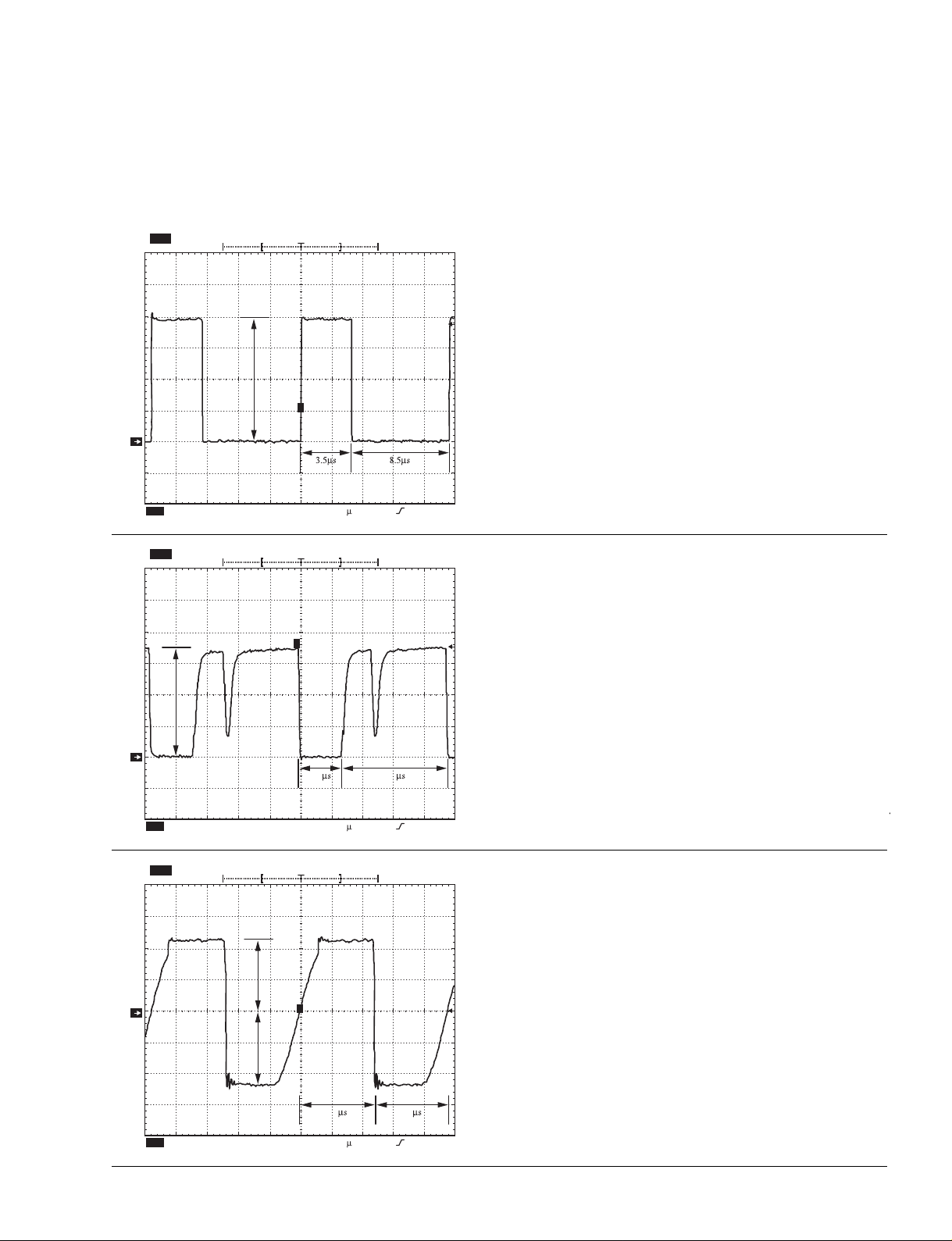
3. WAVE FORM SAMPLE(出力波形)
Sample waveforms that have been referred to in the flow chart are shown after the following page.
(フローチャートで引用されているサンプル波形を示します。)
2431 AcqsTek Stop: 20MS/s
Ch1 Freq
372V
83.41kHz
Ch1 +Duty
33.6%
400V
T
1
Ch1
100V M 2.5 s Ch1
FREQUENCY:
(周波数)
ON DUTY:
Wave form measurement: Circuit Drawing 1/2 “Point B”
(Wave form sample. fig.1)
(波形測定:回路図 1/2 “Point B” 波形サンプル fig.1)
AFC1
83.41KHz
33.6%
181 AcqsTek Stop: 20MS/s
18V
Ch1 Freq
167.5kHz
T
Ch1 +Duty
38.3%
*1
FREQUENCY:
(周波数)
ON DUTY:
167.5KHz
38.3%
Wave form measurement: Circuit Drawing 1/2 “Point D”
1
3.0 9.0
(Wave form sample. fig.2)
(波形測定:回路図 1/2 “Point D” 波形サンプル fig.2)
*1: Operation is actually at 83 KHz. However, measuring unit will
display 167.5 KHz.
Ch1
5V M 2.5 s Ch1
410 AcqsTek Stop: 20MS/s
17.6V
(*1: 実際には83KHzにて動作。測定器都合上167.5KHzに表示)
Ch1 Freq
24V
1
T
83.51kHz
Ch1 +Duty
51%
FREQUENCY:
(周波数)
ON DUTY:
83.51KHz
51.0%
24V
Ch1
10V M 2.5 s Ch1
6.0 6.0
800mV
Wave form measurement: Circuit Drawing 2/2 “Point G”
(Wave form sample. fig.3)
(波形測定:回路図 2/2 “Point G” 波形サンプル fig.3)
17
Page 73

AFC1
20V
66390 AcqsTek Stop: 20MS/s
Ch1 Freq
82.76kHz
FREQUENCY:
82.76KHz
(周波数)
Ch1 +Duty
51%
ON DUTY:
51.0%
20V
T
6.0 6.0
Wave form measurement: Circuit Drawing 2/2 “Point I”
1
(Wave form sample. fig.4)
Ch1
10V M 2.5 s Ch1
464 AcqsTek Stop: 20MS/s
8V
1
T
8V
6.0 6.0
800mV
Ch1 Freq
82.99kHz
Ch1 +Duty
50.9%
(波形測定:回路図 2/2 “Point I” 波形サンプル fig.4)
FREQUENCY:
(周波数)
ON DUTY:
82.99KHz
50.9%
Wave form measurement: Circuit Drawing 2/2 “Point K”
(Wave form sample. fig.5)
Ch1
5V M 2.5 s Ch1
800mV
(波形測定:回路図 2/2 “Point K” 波形サンプル fig.5)
18
188 AcqsTek Stop: 20MS/s
Ch1 Freq
83.45kHz
8V
1
T
8V
6.0 6.0
Ch1 +Duty
48.8%
FREQUENCY:
83.45KHz
(周波数)
ON DUTY:
48.8%
Wave form measurement: Circuit Drawing 2/2 “Point M”
(Wave form sample. fig.6)
Ch1
5V M 2.5 s Ch1
800mV
(波形測定:回路図 2/2 “Point M” 波形サンプル fig.6)
Page 74

AFC1
107 AcqsTek Stop: 20MS/s
Ch1 Freq
20V
1
T
20V
6.0 6.0
83.55kHz
Ch1 +Duty
49.4%
FREQUENCY:
83.55KHz
(周波数)
ON DUTY:
49.4%
Wave form measurement: Circuit Drawing 2/2 “Point O”
(Wave form sample. fig.7)
Ch1
10V M 2.5 s Ch1
760 AcqsTek Stop: 20MS/s
18V
T
1
800mV
Ch1 Freq
83.54kHz
Low signal
amplitude
Ch1 +Duty
20.3%
Low signal
amplitude
(波形測定:回路図 2/2 “Point O” 波形サンプル fig.7)
FREQUENCY:
(周波数)
ON DUTY:
83.54KHz
20.3%
16V
2.5 9.5
Wave form measurement: Circuit Drawing 2/2 “Point Q”
(Wave form sample. fig.8)
Ch1
10V M 2.5 s Ch1
245 AcqsTek Stop: 20MS/s
18V
T
1
18V
3.5 8.5
13.4V
Ch1 Freq
83.46kHz
Low signal
amplitude
Ch1 +Duty
29.8%
Low signal
amplitude
(波形測定:回路図 2/2 “Point Q” 波形サンプル fig.8)
FREQUENCY:
83.46KHz
(周波数)
ON DUTY:
29.8%
Wave form measurement: Circuit Drawing 2/2 “Point S”
(Wave form sample. fig.9)
Ch1
10V M 2.5 s Ch1
13.4V
(波形測定:回路図 2/2 “Point S” 波形サンプル fig.9)
19
Page 75

AFC1
IC1 NBA-0448-O-1
D6
S2L60
R26
150K/F
C16
0.1/50
R15
1K
C11
100/25
D10 S2L60
Q4 2SK2028-01M
D11
1SS133
Q3
2SK2028-01M
C66
27/35
R10
1P100K
D3
1GWJ43
C2
0.1/250
IC2
BA17812T
13
2
R18
47
D1
D3SBA60
R11
1P100K
IC3
FA5332P
9101112131415
16
8765432
1
T1
NT-341F
1
2
3
4
5
7
9
10
12
13
14
15
16
17
18
L2
HR-28-E253
R22
33K
Q1
2SC4615E
R5
100K
C25
2200/250
R30
120K/F
C20 68P/50
Z1
430V
C17
1.0/50
ZD1 MTZJ18B
R1
1M
R29
120K/F
R25
150K/F
C14
10/50
C1
0.47/250V
ZD2MTZJ2.7B
L1
HR-28-E253
R4
4.3
R28
120K/F
C19
0.1/50
R2
220K
D7 S2L60
C22
1000P/50
C9
100/25
R19
82K
TH2
5D-11
C3
0.1/250
FB5
BL02-RN1
CN101
1
2
3
4
5
6
7
8
C21
470P/50
TH1
5D-11
C18
470P/50
R3
2P1K
D4
S3L60
R27
1.3K/F
R48
2P0.27
CN100
1
2
3
D5
S2L60
CN1
B2P3-VH-B
123
R31
1K/F
F1
T2AH250V
C15
100/25
1DL42AD9
D2
ERA15-06V5
R9
1P220K
R17
10
R8
27
R21680K
D8
1DL42A
C10
150/35
R20
22K
R16
10
C13
0.1/50
VR1
2KB
VR2
1KB
R14
10
C7
100/250
R24
150K/F
C4
0.33/250
Q2
2SK1982-01M
R12
2P220
R13
1K
C23
2200P/250
C24
2200P/250
R23
10K
C8
100/250
FB1
BL02-RN1
L3
NL-112
FB4
BL02-RN1
C67
0.01/1K
C12
0.1/50
A
B
C
D
EHG
F
(IC3 10ピン(+)、7ピン(-)にてテスタ−で測定)
(Q2ゲ−ト(H)、Q2ソ−ス(C)にて、オシロスコ−プで測定)
(Q2ドレイン(H)、Q2ソ−ス(C)にて、オシロスコ−プで測定)
(Q3ドレイン(+)、Q4ソ−ス(−)にて、テスタ−で測定)(CN1 1ピンと3ピンにてAC入力電圧をテスタ−で測定)
Measure with tester at IC3 10 pin (+), 7 pin (-).
Point C
Measure with oscilloscope at Q2 gate (H), Q2 source (C).
Point D
Measure with oscilloscope at Q2 drain (H), Q2 source (C).
Point B
Measure with tester at Q3 drain (+), -Q4 source (-).
Point A
Measure AC voltage with tester at CN1 1 pin and 3 pin.
Point E
4. CIRCUIT DIAGRAM(回路図)
Circuit diagrams that have been referred to in the flow chart are shown after the following page.
(フローチャートで引用されている回路図を示します。)
1/2
20
Page 76

+5V
GND(+5V)
+3.3V
GND(+3.3V)
GND(+3.3V)
GND(+3.3V)
GND(+5V)
GND(+5V)
+5V
+5V
+3.3V
+3.3V
+15V
GND
+15V
+15V
-15V
-15V
+5V
+5V
-5V
-5V
+5V
+5V
GND(DG)
GND(AG)
+20V
L7
NL-116
R44
470
C42
470/10
L11
NL-067
D32
1SS133
D22 ERA15-06V5
Q5
2SB1241R
D15
D1NS6
D17
1SS133
C27
220/35
R42
1K
D20 1SS133
C36
220/25
D14
D1NS6
C35
0.1/50
L4
NL-116
L8
NL-116
D23 ERA15-06V5
SW2 RGE700
C48470/10
C28
0.1/50
L9
NL-111
IC5
BA17815T
13
2
D16
D1NS6
D27
30GWJ2CZ47C
C37
0.1/50
D19
1SS133
C30 220/25
L5
NL-116
SW1 RGE400
R47
2.7KF
C56
220/25
D28
30GWJ2CZ47C
IC8
TA79015S
32
1
R36
22
C32
220/35
C34
0.1/50
IC9
TA76431S
FB8
BL02-RN1
C60
0.1/50
C29
0.1/50
R45
1K
R46
2.2KF
R38
4.3
D13
D1NS6
D31
1SS133
VR4
1KB
C63
470P/50
FB9
BL02-RN1
C52 0.1/50
C43
0.1/50
R37
470
IC7
TA79005S
32
1
R41
1P100
C50
220/35
D18
1SS133
CN4
B8B-PH-K-S
1234567
8
L12
NL-100
C62
0.47/50
IC6
BA05T
13
2
C26
220/35
C46 0.1/50
D30
D1NL40
R43
22
B13B-PH-K-S
CN2
12345678910111213
CN5
B4P-VH
123
4
C51
150/35
L10
NL-110
C59
470/10
C64
0.47/50
D29
D1NL40
C45
220/25
C54
220/25
FB11
BL02-RN1
D26 ERA15-06V5
C49
0.1/50
C65
0.01/50
C57
100/20
D21 1SS133
C58
220/25
C55
0.1/50
FB12
BL02-RN1
D25
ERA15-06V5
SW3 RUE400
R34
1P22
L13
NL-102
C53 0.1/50
C38
330/35
C33
150/35
C31 0.1/50
C39
220/25
R35
1K
IC10
TA76431S
D12
1GU42
C44
220/35
C61
0.1/50
D24
ERA15-06V5
C40
0.1/50
VR3
1KB
Q6
2SB1241R
C47 0.1/50
L6
NL-116
CN3
B2B-PH-K-S
1
2
PR1
ICP-N50
C41
0.1/50
R33
1P100
PR4 ICP-50
IC4
BA17820T
13
2
FB10
BL02-RN1
PR5 ICP-N50
PR3 ICP-N50
R32
330
L14
ONL-012
R39
270F
PR2 ICP-N50
FB6
BL02-RN1
FB7
BL02-RN1
R40
2.4KF
A
B
C
D
E
F
G
H
(D14のア ノ−ド(H)、IC6 GNDピン(C)
にて、オシロスコ−プで測定)
Measure with oscilloscope at
D14 anode (H), IC6 GND pin (C).
Measure with oscilloscope at D13 anode (H), IC5 GND pin (C).
Measure with oscilloscope at D29 cathode (H), IC7 GND pin (C).
Point K
Point M
Measure with oscilloscope
at D29 cathode (H), FG harness (C).
Measure with oscilloscope
at D30 cathode (H), FG harness (C).
Point S
Measure with oscilloscope
at D16 cathode (H), IC8 GND pin (C).
Point O
Point G
Point I
Measure with oscilloscope at D12 anode (H), IC4 GND pin (C).
Point F
Measure with tester
at CN2 13 pin (+), 11 pin (-).
Point H
Measure with tester
at CN2 1 pin (+), 11 pin (-).
Point J
Measure with tester
at CN2 5 pin (+), 11 pin (-).
Point L
Measure with tester
at CN2 7 pin (+), 11 pin (-).
Point N
Measure with tester
at CN2 4 pin (+), 11 pin (-).
Point P
Measure with tester
at CN5 3 pin (+), 4 pin (-).
Point R
Measure with tester
at CN5 1 pin (+), 4 pin (-).
(CN2 13ピン(+)、11ピン(-)
にて、テスタ−で測定)
(CN2 1ピン(+)、11ピン(-)
にて、テスタ−で測定)
(CN2 5ピン(+)、11ピン(-)
にて、テスタ−で測定)
(CN2 7ピン(+)、11ピン(-)
にて、テスタ−で測定)
(CN2 4ピン(+)、11ピン(-)
にて、テスタ−で測定)
(CN5 3ピン(+)、4ピン(-)
にて、テスタ−で測定)
(CN5 1ピン(+)、4ピン(-)
にて、テスタ−で測定)
(D30のカソ−ド(H)、FGハ−ネス(C)
にて、オシロスコ−プで測定)
(D29のカソ−ド(H)、FGハ−ネス(C)
にて、オシロスコ−プで測定)
Point Q
(D15のカソ−ド(H)、IC7 GNDピン(C)にて
オシロスコ−プで測定)
(D12のアノ−ド(H)、IC4 GNDピン(C)にて、オシロスコ−プで測定)
(D13のアノ−ド(H)、IC5 GNDピン(C)にて、オシロスコ−プで測定)
(D16のカソ−ド(H)、IC8 GNDピン(C)
にて、オシロスコ−プで測定)
2/2
AFC1
21
Page 77

AFC1
5. PARTS LIST
REF NO. PART NO. DESCRIPTION REMARKS QTY
AAX40850
D3 Diode 1GWJ43
D11 Diode 1SS133
D17 Diode 1SS133
D18 Diode 1SS133
D19 Diode 1SS133
D20 Diode 1SS133
D21 Diode 1SS133
D27 Twin Diode SBD 30GWJ2CZ47C
D28 Twin Diode SBD 30GWJ2CZ47C
D29 Diode LLD DINL40
D30 Diode LLD DINL40
D31 Diode 1SS133
D32 Diode 1SS133
F1 Fuse T2AH250V 215002
IC1 HIC Assembly NBA-0448-0-1
IC2 IC BA17812T REGULATOR
IC3 IC FA5332P PFC Controller
IC4 IC BA17820T REGULATOR
IC5 IC BA17815T REGULATOR
IC6 IC BA05T REGULATOR
IC7 IC TA79005S REGULATOR
IC9 IC TA76431S REGULATOR
IC10 IC TA76431S REGULATOR
PR1 IC Protector ICP-N50
PR2 IC Protector ICP-N50
PR3 IC Protector ICP-N50
PR4 IC Protector ICP-N50
PR5 IC Protector ICP-N50
Q1 Transistor 2SC4615E
Q2 FET 2SK1982-01M
Q3 FET 2SK2028-01M
Q4 FET 2SK2028-01M
Q5 Transistor 2SB1241R
Q6 Transistor 2SB1241R
R3 Metal Oxide Film Resistor 2P1K ERG2SJ102E
R4 Carbon Resistor 4.3 R20T-24J 4R3
R14 Carbon Resistor 10 R20T-24J 100
R16 Carbon Resistor 10 R20T-24J 100
R17 Carbon Resistor 10 R20T-24J 100
R38 Carbon Resistor 4.3 R20T-24J 4R3
ZD1 Zener Diode MTZJ18B
ZD2 Zener Diode MTZJ2.7B
(パーツリスト)
PS UNIT PARTS KIT AFC1
Circuit Board NB-0449-0-3
部品名
PSユニットパーツキット
メインシート
ダイオード
ダイオード
ダイオード
ダイオード
ダイオード
ダイオード
ダイオード
ツインダイオード
ツインダイオード
ダイオード
ダイオード
ダイオード
ダイオード
ヒューズ
HICたて基板Assy
I C
I C
I C
I C
I C
I C
I C
I C
I C プロテクタ
I C プロテクタ
I C プロテクタ
I C プロテクタ
I C プロテクタ
トランジスタ
F E T
F E T
F E T
トランジスタ
トランジスタ
酸化金属被膜抵抗
カーボン抵抗
カーボン抵抗
カーボン抵抗
カーボン抵抗
カーボン抵抗
ツェナーダイオード
ツェナーダイオード
RANK
22
: New Parts
RANK: Japan only
Page 78

AFC1
6. INSPECTION & ADJUSTMENT
1. After replacing the defective parts, follow the flow chart for
each output voltage system and perform the inspections and
adjustments shown after 2.
2. Check each output voltage without a load and, if necessary,
use the adjustment volume to make fine adjustments.
3. Check each output voltage with the rated load and, if
necessary, use the adjustment volume to make fine
adjustments.
4. The following shows the rated output voltage values,
locations for measuring the output voltage and relevant
volumes for adjustment.
rated output voltage
values (V)
+5V +/-5% CN5-1pin/CN5-4pin VR4
+3.3V +/-5% CN5-3pin/CN5-4pin VR3
+5V +/-5% CN2-5pin/CN2-11pin -
-5V +/-5% CN2-7pin/CN2-11pin -
+15V +/-5% CN2-1pin/CN2-11pin -
-15V +/-10% CN2-4pin/CN2-11pin +20V +/-5% CN2-13pin/CN2-11pin -
Locations for measuring Relevant volumes for
the output voltage adjustment
6. 調整・検査
1.不良パーツ交換後、各出力電圧系統のフローチャート
に従って、2 以降の調整・検査を行ないます。
2.無負荷時の各出力電圧を確認し、必要に応じて調整用
ボリュームにて、微調整を行ないます。
3.定格負荷時の各出力電圧を確認し、必要に応じて調整
用ボリュームにて、微調整を行ないます。
4.以下に規定出力電圧値、出力電圧の測定場所及び、該
当する調整用ボリュームを示します。
規定出力電圧値(V)
+5V+/-5% CN5-1pin/CN5-4pin間 VR4
+3.3V+/-5% CN5-3pin/CN5-4pin間 VR3
+5V+/-5% CN2-5pin/CN2-11pin 間 調整なし
-5V+/-5% CN2-7pin/CN2-11pin 間 調整なし
+15V+/-5% CN2-1pin/CN2-11pin間 調整なし
-15V+/-10% CN2-4pin/CN2-11pin間 調整なし
+20V+/-5% CN2-13pin/CN2-11pin 間 調整なし
測定場所 調整用ボリューム
23
Page 79

ACTIVE FIELD CONTROLLER
CIRCUIT DIAGRAM
CONTENTS
BLOCK DIAGRAM (002~003) ......... 3
WIRING ........................................... 5
CIRCUIT DIAGRAM
POWER SUPPLY UNIT BLOCK DIAGRAM
POWER SUPPLY UNIT CIRCUIT DIAGRAM
Notation for Circuit Diagrams
1. How to identify inter-sheet connectors
Signal name
(信号名)
(総コネクタ接続回路図)
MAIN (002~020) ............................................................. 6
SUB ................................................................................. 6
PNF (LED)...................................................................... 25
PNF (PSW) .................................................................... 25
PNR (MYMB) ................................................................ 26
PNR (GPI) ...................................................................... 27
/MRD
(目次)
(ブロックダイアグラム)
(回路図)
(電源ユニットブロックダイアグラム)
(電源ユニット回路図)
(回路図表記上の注意)
(シート間コネクタの読み方について)
003: L11
The 3-digit number indicates the destination page.
(3桁の数字は信号の行先ページ数を示します。)
This indicates the location of the counter inter-sheet connector.
(The alphabet indicates horizontal direction and the number
indicates vertical direction.)
対応するシート間コネクタのあるロケーションを示します。
(アルファベットが水平方向、数字が垂直方向)
........................................ 29
............... 28
Note: See parts list for details of circuit board component parts.
注:シートの部品詳細はパーツリストをご参照ください。
Page 80

BLOCK DIAGRAM 002 (AFC1)
MAIN
p.9
JK001
MIDI IN
MIDI OUT
IC020 (8P),
IC019 (14P)
MIDTX
MIDRX
CPU
IC004
(112p)
A/D
91-94 52-70 84
107 108
GPIIN[0-3]
GPI receiver
IC044,IC045
(16P)
p.13
CN010 (36P) CN010 (36P)
p.6
GPISEL[0,1]
IC046-049
IC50,51
CN701 (36P)
PNR (GPI)
X001
7MHz
47 48 72 74
RES
RES7RES
D[0-15]
GPI driver
(16P)
(20P)
p.13
7
Reset
Backup
Controller
IC002
(8P)
RES
RES
RES
p.6
/RESET[2]
BATTERY BACKUP
FLASH ROM
8Mbit
(44p) (32p)(32p)(32p) (32p) (32p) (32p) (32p) (32p)
IC006
p.7
RESET
44 12 22
/RESET[1]
/SCS
8
7
7
5
/MRD,/WRL
D[0-15],A[1-19]
/RESET[2]
/RESET[1]
CE
SRAM
1Mbit
IC007
p.7
/MRD,/WRL
D[0-7],A[1-17]
9
10
12
13
/SCNCS2
/SCNCS1
/FMCS
/GPIWR
CE1
IC003
(14P)
p.6
IC003
(14P)
p.6
/SCS1
85
86
87
51
SRAM
1Mbit
IC008
p.7
/MRD,/WRH
D[8-15],A[1-17]
/SCS1
8
/SCS2
11
I85
I86
I87
I51
CE1
22
/SCS1
SRAM
1Mbit
IC009
CE1
p.7
/MRD,/WRL
D[0-7],A[1-17]
Selector (FPGA)
22
/SCS2
91
I91
IC015
(100P)
SRAM
1Mbit
IC010
p.7
/MRD,/WRH
D[8-15],A[1-17]
SRAM
1Mbit
IC011
CE1
22
/SCS2
/MRD,/WRL
D[0-7],A[1-17]
D[0-3]
A[18,19,21]
A[1-7,12-15]
p.8
CN003 CN002
CONTROL
p.7
I63
I65
CE2
30
/SCS3
63
65
PC
15
CE1
/SCS
RPTX
RPRX
22
/MRD,/WRH
39
2D
Driver
Receiver
IC021
(16p)
p.9
SRAM
1Mbit
IC012
CE2
p.7
30
/SCS3
D[8-15],A[1-17]
RESET
RESET
39
TXC
FOR
SERVICE USE
SRAM
1Mbit
IC013
CE1
22
/SCS
10 20 41 51 26
CASOUTTX
/MRD,/WRL
D[0-7],A[1-17]
UART
IC018
(64P)
CASOUTRX
to
OUT
CASCADE
CE2
p.7
/SCS4
IC16,17
19.6608MHz
MYTX
30
X002
XTAL1
MYRX
to
CE1
22
/SCS
/MRD,/WRH
2527
p.9
38.4kbps
MY slot 1
SRAM
1Mbit
IC014
CE2
p.7
D[8-15],A[1-17]
/RESET[1]
9.8MHz
Driver
Driver
CE1 A1
22
30
/SCS
/SCS4
D[0-7]
/LEDSET
IC023
(20p)
11
CLOCK
CLEAR
1
p.10
TA001
(18p)
p.10
CN005
(10P) (10P)
IC111
p.23
A[1-8]
CNTSTX,CNTSRX
LED driver
CN401 (10P)
LED
IC112
p.23 p.23 p.23 p.23 p.23
A[9-16]
/RESET[1]
10,11
PNF (LED)
Driver
IC113
A[0,17-19,21]
/SCSET
IC024
(16p)
9
CLK
CLR
1
p.10
TA002 16p
I5,I6
p.10
CN005
CKIO
/CS2,DACK[0]
/WRH,/WRL,/RD
D[0-3]
receiver
switch,LED
Driver
IC114
A79A8
/RESET[2]
/SWRD
19
10
/BS,/USBCS
IC031
(20p)
G
p.10
Driver
Receiver
IC115
/PCMCS
D[0-7],/RD
D[0-7]
SW driver
Receiver
G
22
D[8-15],/RD
/RD
Driver
IC116
/LCDGATE
/RD
Receiver
IC117
(24p)(24p)(24p)(24p)(24p)(24p)(24p)
G
p.23
223
/PCMCS
/DREQ[0],SUSPEND
G
IC030
(20p)
p.10
A4-6
/PCMWAIT
D[0-7]
7,86
/USBINT
/PCMINT
LCD driver
BCDEFG
A
AFC1
1
CPU BUS
FPGA BUS
DSP BUS
2
A[12-14]
/DSPWAIT1
A[12-14]
/DSPWAIT2
A[12-15]
/DSPCS
A[12-15]
/DSPCS
/WRL,/RD /WR1,/RD1,/RST1
/DSPRST
A[1-7]
A[1-7]
D[0-7],/RD
/DSPEN1
D[8-15],/RD
/DSPEN1
D[0-7],/RD
/DSPEN2
D[8-15],/RD
/DSPEN2
Selector
IC062(16p)
p.15
Selector
IC063(16p)
p.15
Decoder
IC064(16p)
p.15
Decoder
IC065(16p)
p.15
Driver
IC067(20p)
p.15
Driver
IC068(20p)
p.15
Driver
IC069(20p)
p.15
Driver
IC070(20p)
p.15
Driver
IC071(20p)
p.15
Driver
IC072(20p)
p.15
Driver
IC073(20p)
p.15
/D6WAIT[1-8]
/D6WAIT[9-10]
/D5WAIT[1-3]
/D6CS[1-8]
/D6CS[9-10]
/D5CS[1-3]
/WR2,/RD2,/RST2
A[101-107]
A[201-207]
D[100-107]
D[108-115]
D[200-207]
D[208-215]
3
4
5
28CA1-8828138-002
Note: “P.**” shows the page number in the circuit diagrams of the Main circuit board (AFC1).
注:p.**はシートMAIN回路図(AFC1)中のページ番号を示します。
CPU Section
BLOCK DIAGRAM 002 (AFC1)
3
6
Page 81

ABCDEFGH
BLOCK DIAGRAM 003 (AFC1)
CPU BUS
1
2
3
4
5
6
FPGA BUS
MAIN
4
/RST1
/WR1
/RD1
DSP BUS
A[101-107]
D[100-115]
A[201-207]
D[200-215]
/RST2
/WR2
/RD2
/D6CS[1-10]
/D5CS[1-3]
/D6WAIT[1-10]
/D5WAIT[1-3]
28CA1-8828138-003
Driver
IC074
(20p)
(20p)
IC075
p.16
SYNCI[1],CKI[1]
/D6CS[1]
/D6WAIT[1]
SYNCI[1],CKI[1]
/D6CS[2]
/D6WAIT[2]
SYNCI[2],CKI[2]
/D6CS[3]
/D6WAIT[3]
SYNCI[2],CKI[2]
/D6CS[4]
D6WAIT[4]
SYNCI[4],CKI[4]
/D6CS[7]
/D6WAIT[7]
SYNCI[4],CKI[4]
/D6CS[8]
/D6WAIT[8]
SYNCI[5],CKI[5]
/D6CS[9]
/D6WAIT[9]
SYNCI[5],CKI[5]
/D6CS[10]
/D6WAIT[10]
/SYNCO,CKO
DSP6
DRAM
16Mbit x 2
IC076,IC078
(42p) (42p)
DSP6 IC080(176p)
DRAM
16Mbit x 2
IC079,IC081
(42p) (42p)
DSP6 IC083(176p)
DRAM
16Mbit x 2
IC082,IC084
(42p) (42p)
DSP6 IC086(176p)
DRAM
16Mbit x 2
IC085,IC087
(42p) (42p)
DSP6 IC095(176p)
DRAM
16Mbit x 2
IC094,IC096
(42p) (42p)
DSP6 IC098(176p)
DRAM
16Mbit x 2
IC097,IC099
(42p) (42p)
DSP6 IC101(176p)
DRAM
16Mbit x 2
IC100,IC102
(42p) (42p)
DSP6 IC104(176p)
DRAM
16Mbit x 2
IC103,IC105
(42p) (42p)
X004
60MHz
IC077(176p)
D51S[16-19]
D51S[20-23]
p.16
D51S[24-27]
D51S[28-31]
p.16
D51S[32-35]
D51S[36-39]
p.17
D51S[40-43]
D51S[44-47]
p.17
D52S[16-19]
D52S[20-23]
p.19
D52S[24-27]
D52S[28-31]
p.19
D52S[32-35]
D52S[36-39]
p.20
D52S[40-43]
D52S[44-47]
p.20
SYNCI[6],CKI[6]
10 13
10 13
SYNCI[6],CKI[6]
p.21
DSP5
IC106
(208p)
D51S[0-3]
IC
19
19
IC
D51S[4-7]
DSP5
IC107
(208p)
/RST2,/WR2,/RD2/RST2,/WR2,/RD2
/D5CS[1],/D5WAIT[1]/D5CS[2],/D5WAIT[2]
WR RD CS
27 28
27 28
WR RD
CS
MCKD
SSYNC1718
FS128_2,SSYNC2
FS128_1,SSYNC1
p.21
26
26
D51S[48-51]
DSP6 IC089(176p)
DRAM
D51S[52-55]
p.18
D51S[56-59]
D51S[60-63]
p.18
D51S[8-11]
D51S[12-15]
17
MCKD MCKD
WAIT
65
D52S[8-11]
D52S[12-15]
16Mbit x 2
IC088,IC090
(42p) (42p)
DSP6 IC092(176p)
DRAM
16Mbit x 2
IC091,IC093
(42p) (42p)
X003
24.576MHz
(Fs=48kHz)
IC22
FS256_1,SSYNC2
BUSOUT[1-4]
BUSOUT[5-8]
9.8MHz
/RESET[1]
17
10
13
26
CS
65
WAIT
Driver
IC066 (20p)
p.15
SYNCI[3],CKI[3]
/D6CS[5]
/D6WAIT[5]
SYNCI[3],CKI[3]
/D6CS[6]
/D6WAIT[6]
DSP5
IC110
(208p)
SYNCI[6],CKI[6]
/D5CS[3],/D5WAIT[3]
5,6 2 22 23
Selector
IC027(16p)
p.10
FS256
FS128
SSYNC
Selector
IC108
IC109
p.21
(16p)
(16p)
6-10
/CONMY1-4
MY slot BUS
p.22
SIN[1-4]
SIN[5-8]
SOUT[1-4]
SOUT[5-8]
SIN[9-12]
SIN[13-16]
SOUT[9-12]
SOUT[13-16]
FS256, FS128
FS64, FS, SSYNC
WCKIN
DIR2
IC028(44p)
36
p.10
CBUS[1-4]
CBUS[5-8] IC038
2ch/line x 4 (AUDIO)
4ch/line x 4 (AUDIO)
8ch/line x 4 (AUDIO)
8,9
/MYCS[1-4]
Transceiver
IC052
Transceiver
IC058
Transceiver
IC060
Transceiver
IC059
Transceiver
IC061
Selector
5
IC026(16p)
Buffer
IC029(20p)
p.10
CFS256
CFS128
ATSC x2
IC042
Receiver
p.24
Driver
p.24
IC043(16p)
IC036(16p)
A[1-8]
Transceiver
IC055
p.14
Driver
p.12
Driver
p.11
Receiver
IC033(16p)
IC032(16p)
p.11
Driver
IC035(16p)
IC034(16p)
p.11
A[9-10]
Transceiver
IC056
CN015
sum in
bus out
CASINWCIN
CASINWCOUT
CASOUT
WCOUT
CASOUT
WCIN
bus in
sum out
SSYNC
FS64, FS,
FS256, FS128
p.14
CASCADE IN
JK002
JK003
CN009
CASCADE OUT
CONTROL
WORD CLOCK IN
WORD CLOCK OUT
CONTROL
/MYCS
/RD,/WRL,/WRH
19 19 2 6 12 7
Transceiver
IC053
(20p) (20p) (20p) (20p) (20p) (20p)
p.14
p.14
p.14
p.14
p.14
p.10
CFS64
CSSYNC
(20p)
(20p)
(20p)
(20p)
12
18
(80p)
(80p)
SUMOUT[1-4]
SUMOUT[5-8]
S1OUT[1-8]
S2OUT[1-8]
S3OUT[1-8]
S4OUT[1-8]
CASWCIN
WCIN
CFS256
DIR2
IC040(44p)
p.12
MCC
CSYNC
MCA,MCB
p.14
S1IN[1-8]
S2IN[1-8]
S3IN[1-8]
S4IN[1-8]
5
p.12
/MYCS
/RD,D[0-7]
MYRX1
MYTX1
/MY1IRQ
MY slot 1 MY slot 2 MY slot 3 MY slot 4
SUMIN[1-4]
SUMIN[5-8]
BUSOUT[1-4]
BUSOUT[5-8]
Receiver
IC039(16p)
p.12
Transceiver
IC054
p.14
OUT1
OUT2
BUSIN[1-4]
BUSIN[5-8]
/RD,D[8-15]
IC121(16p)
IC120(16p)
IC119(16p)
IC118(16p)
WC
WC
DSP Section
BLOCK DIAGRAM 003 (AFC1)
/MYIRQ
Transceiver
IC057
p.14
TX
RX
TX
RX
AFC1
MYTX,MYRX
Driver
Receiver
IC122(16p)
p.24
CASIN_ID
/LOCK (LOCKN)
CASOUT_ID
Driver
Receiver
IC037(16p)
p.11
/RESET[2]
MYWC1-4
DIAGOUT
WCKIN
WCSEL[0-2]
CASIN
TX
RX
/CASLOCK
CASOUT
TX
RX
BUSOSEL
Page 82

MAIN
WIRING (AFC1)
OPEN
OPEN
OPEN
FOR SERVICE USE
PNF (LED)
PNR (GPI)
PNR (MYMB)
BCDEFGHIJKLMNOP
A
AFC1
1
2
3
4
5
TO SERVICE PERSONNEL
Critical Components Information
Components having special characteristics
are marked and must be replaced with
parts having specifications equal to those
originally installed.
PNF (PSW)
AC Inlet
OPEN
OPEN
POWER SUPPLY
Primary
2A
F1
OPEN
OPEN
Secondary
PATTERN/
LIVENESS
6
7
8
9
OPEN
10
KEC-92548
11
1
WIRING (AFC1)
12
5
Page 83

ABCDEFGHIJKLMNOP
MAIN, SUB CIRCUIT DIAGRAM 002 (AFC1)
AFC1
1
OP AMP
2
OR
3
SYSTEM
Battery
RESET
socket
OR
4
SUB
AND NAND
5
SYSTEM RESET
6
7
8
9
10
11
28CC1-8825995
OP AMP
TO SERVICE PERSONNEL
Critical Components Information
Components having special characteristics are marked
and must be replaced with parts having specifications
equal to those originally installed.
• Lithium Battery(リチウム電池)
Battery VN103500
VN103600(Battery holder for VN103500)
Notice for back-up battery removal
Push the battery as shown in figure,
then the battery will pop up.
Druk de batterij naar beneden zoals
aangeven in de tekening de batterij
springt dan naar voren.
Battery
Battery holder
CPU (MASK)
OR
Note) R007 and R010 are not installed. (for mode set)
注)R007、R010は実装なし(モード設定用)
: Ceramic Capacitor
(
セラミックコンデンサー
)
12
KEC-92549-002
15
MAIN, SUB CIRCUIT DIAGRAM 002 (AFC1)
6
Page 84

MAIN CIRCUIT DIAGRAM 003 (AFC1)
FLASH ROM 8M SRAM 1M
SRAM 1M
BCDEFGHIJKLMNOP
A
AFC1
1
2
3
4
5
SRAM 1M
SRAM 1M
SRAM 1M
SRAM 1M
6
7
SRAM 1M
8
9
SRAM 1M
10
KEC-92549-003
10
Note) R011 – R014 and R019 – R022 are not installed. (for mode set)
注)R011〜R014、R019〜R022は実装なし(モード設定用)
: Ceramic Capacitor
MAIN CIRCUIT DIAGRAM 003 (AFC1)
(
セラミックコンデンサー
11
)
12
7
Page 85

ABCDEFGHIJKLMNOP
1
MAIN CIRCUIT DIAGRAM 004 (AFC1)
AFC1
2
3
4
5
6
7
8
9
10
OPEN
FPGA
: Ceramic Capacitor
(
セラミックコンデンサー
)
11
12
Note) R023 is not installed. (for mode set)
注)R023は実装なし(モード設定用)
KEC-92549-004
8
6
MAIN CIRCUIT DIAGRAM 004 (AFC1)
Page 86

MAIN CIRCUIT DIAGRAM 005 (AFC1)
UART
LINE DRIVER
/RECEIVER
BCDEFGHIJKLMNOP
A
AFC1
1
2
3
4
INVERTER
D-FF
Photo Coupler
INVERTER INVERTERD-FF
5
6
7
8
9
KEC-92549-005
13
INVERTER
: Ceramic Capacitor
(
セラミックコンデンサー
)
MAIN CIRCUIT DIAGRAM 005 (AFC1)
10
11
12
9
Page 87

ABCDEFGHIJKLMNOP
1
MAIN CIRCUIT DIAGRAM 006 (AFC1)
AFC1
2
DATA SELECTOR
3
DIR2
BUFFER
4
5
DATA SELECTOR
D-FF
D-FF
6
7
8
9
10
SWITCH, LED
RECEIVER
LED DRIVER
INVERTER
OPEN
to PNF (LED)-CN401
OPEN
SW DRIVER
OPEN
INVERTER
OPEN
11
12
10
KEC-92549-006
17
: Ceramic Capacitor
: Mylar Capacitor (C053)
(
セラミックコンデンサー
(
マイラーコンデンサー
: Metal Oxide Film Resistor (R063)
)
)
(
酸化金属被膜抵抗
LCD DRIVER
)
MAIN CIRCUIT DIAGRAM 006 (AFC1)
Page 88

MAIN CIRCUIT DIAGRAM 007 (AFC1)
LINE RECEIVER
BCDEFGHIJKLMNOP
A
AFC1
1
2
3
4
LINE RECEIVER
LINE DRIVER
LINE DRIVER
5
6
7
8
LINE DRIVER
/RECEIVER
9
KEC-92549-007
10
LINE DRIVER
: Ceramic Capacitor
(
セラミックコンデンサー
)
11
6
MAIN CIRCUIT DIAGRAM 007 (AFC1)
11
12
Page 89

ABCDEFGHIJKLMNOP
1
MAIN CIRCUIT DIAGRAM 008 (AFC1)
AFC1
2
3
ATSCATSC
4
5
6
7
8
9
10
LINE RECEIVER
DIR2
SINGLE SHOT
LINE DRIVER
OR
INVERTER
11
12
12
KEC-92549-008
OR INVERTER
: Ceramic Capacitor
6
: Mylar Capacitor (C078)
(
セラミックコンデンサー
(
マイラーコンデンサー
)
)
MAIN CIRCUIT DIAGRAM 008 (AFC1)
Page 90

to PNR (GPI)-CN701
MAIN CIRCUIT DIAGRAM 009 (AFC1)
MULTIPLEXER
D-FF
TRANSCEIVER
AFC1
A
1
BCDEFGHIJKLMNOP
2
3
4
MULTIPLEXER
D-FF
D-FF
D-FF
5
6
TRANSCEIVER
7
8
9
KEC-92549-009
10
: Ceramic Capacitor
7
(
セラミックコンデンサー
MAIN CIRCUIT DIAGRAM 009 (AFC1)
)
13
11
12
Page 91

ABC
MAIN CIRCUIT DIAGRAM 010 (AFC1)
EFGHIJKLMNOP
D
AFC1
1
2
TRANSCEIVER
3
TRANSCEIVER
to PNR (MYMB)-CN605
to PNR (MYMB)-CN607
4
TRANSCEIVER
5
TRANSCEIVER
6
TRANSCEIVER
TRANSCEIVER
7
to PNR (MYMB)-CN608
8
TRANSCEIVER
to PNR (MYMB)-CN606
9
10
11
12
14
KEC-92549-010
TRANSCEIVER
: Ceramic Capacitor
6
(
セラミックコンデンサー
TRANSCEIVER
)
TRANSCEIVER
MAIN CIRCUIT DIAGRAM 010 (AFC1)
Page 92

MAIN CIRCUIT DIAGRAM 011 (AFC1)
DATA SELECTOR
DATA SELECTOR
DRIVER
DRIVER
BCDEFGHIJKLMNOP
A
AFC1
1
2
3
4
5
DECODER
DECODER
DRIVER
DRIVER
DRIVER
DRIVER
DRIVER
DRIVER
6
7
8
9
10
KEC-92549-011
11
6
: Ceramic Capacitor
(
セラミックコンデンサー
)
MAIN CIRCUIT DIAGRAM 011 (AFC1)
12
15
Page 93

ABCDEFGHIJKLMNOP
MAIN CIRCUIT DIAGRAM 012 (AFC1)
AFC1
1
DRAM 16M DRAM 16M DRAM 16M DRAM 16M
2
3
4
5
6
7
8
9
10
DRIVER
DSP6 DSP6
DRIVER
11
12
16
KEC-92549-012
11
: Ceramic Capacitor
(
セラミックコンデンサー
)
MAIN CIRCUIT DIAGRAM 012 (AFC1)
Page 94

MAIN CIRCUIT DIAGRAM 013 (AFC1)
BCDEFGHIJKLMNOP
DRAM 16MDRAM 16MDRAM 16MDRAM 16M
AFC1
A
1
2
3
4
DSP6 DSP6
5
6
7
8
9
KEC-92549-013
11
: Ceramic Capacitor
(
セラミックコンデンサー
10
11
)
MAIN CIRCUIT DIAGRAM 013 (AFC1)
17
12
Page 95

ABCDEFGHIJKLMNOP
MAIN CIRCUIT DIAGRAM 014 (AFC1)
AFC1
1
DRAM 16MDRAM 16MDRAM 16MDRAM 16M
2
3
4
5
6
7
8
9
10
DSP6 DSP6
11
12
18
KEC-92549-014
11
: Ceramic Capacitor
(
セラミックコンデンサー
)
MAIN CIRCUIT DIAGRAM 014 (AFC1)
Page 96

MAIN CIRCUIT DIAGRAM 015 (AFC1)
BCDEFGHIJKLMNOP
A
AFC1
1
DRAM 16MDRAM 16MDRAM 16MDRAM 16M
2
3
4
DSP6 DSP6
5
6
7
8
9
KEC-92549-015
11
: Ceramic Capacitor
(
セラミックコンデンサー
)
MAIN CIRCUIT DIAGRAM 015 (AFC1)
19
10
11
12
Page 97

ABCDEFGHIJKLMNOP
MAIN CIRCUIT DIAGRAM 016 (AFC1)
AFC1
1
DRAM 16MDRAM 16MDRAM 16MDRAM 16M
2
3
4
5
6
7
8
9
10
DSP6 DSP6
11
12
20
KEC-92549-016
11
: Ceramic Capacitor
(
セラミックコンデンサー
)
MAIN CIRCUIT DIAGRAM 016 (AFC1)
Page 98

MAIN CIRCUIT DIAGRAM 017 (AFC1)
DSP5 DSP5
BCDEFGHIJKLMNOP
A
AFC1
1
2
3
4
SELECTOR
5
6
7
8
9
KEC-92549-017
10
: Ceramic Capacitor
6
SELECTOR
MAIN CIRCUIT DIAGRAM 017 (AFC1)
(
セラミックコンデンサー
)
21
11
12
Page 99

ABCDEFGHIJKLMNOP
1
MAIN CIRCUIT DIAGRAM 018 (AFC1)
AFC1
2
3
4
5
6
7
8
9
10
DSP5
11
12
22
KEC-92549-018
: Ceramic Capacitor
6
MAIN CIRCUIT DIAGRAM 018 (AFC1)
(
セラミックコンデンサー
)
Page 100

MAIN CIRCUIT DIAGRAM 019 (AFC1)
TRANSCEIVER
TRANSCEIVER
OPEN
TRANSCEIVER
TRANSCEIVER
BCDEFGHIJKLMNOP
AFC1
A
1
2
3
4
5
from POWER SUPPLY UNIT-CN5
TRANSCEIVER
TRANSCEIVER
OPEN
TRANSCEIVER
6
7
8
9
10
KEC-92549-019
11
: Ceramic Capacitor
6
MAIN CIRCUIT DIAGRAM 019 (AFC1)
(
セラミックコンデンサー
)
12
23
 Loading...