

Yaesu FT-817 Service Manual
HF / VHF / UHF
All Mode Transceiver
FT-817
Technical Supplement
©2003 VERTEX STANDARD CO., LTD. Printed in Japan.
(E137790A)
Introduction
This manual provides technical information necessary for
servicing the Yaesu FT-817 HF & V/UHF-Bands Transceiver. It does not include information on installation and
operation, which are described in the FT-817 Operating
Manual provided with the transceiver, or on accessories
which are described in their manuals.
The FT-817 is carefully designed to allow the knowledgeable operator to make nearly all adjustments required for
various station conditions, modes and operator preferences simply from the controls on the panels, without opening the case of the transceiver. The FT-817 Operating Manual describes these adjustments, plus certain internal settings.
Servicing this equipment requires expertise in handling
surface mount chip components. Attempts by unqualified
persons to service this equipment may result in permanent damage not covered by warranty. For the major circuit boards, each side of the board is identified by the type
of the majority of components installed on that side. In
most cases one side has only chip components, and the
other has either a mixture of both chip and lead compo-
VERTEX STANDARD CO., LTD.
4-8-8 Nakameguro, Meguro-Ku, Tokyo 153-8644, Japan
VERTEX STANDARD
US Headquarters
10900 Walker Street, Cypress, CA 90630, U.S.A.
International Division
8350 N.W. 52nd Terrace, Suite 201, Miami, FL 33166, U.S.A.
YAESU EUROPE B.V.
P.O. Box 75525, 1118 ZN Schiphol, The Netherlands
YAESU UK LTD.
Unit 12, Sun Valley Business Park, Winnall Close
Winchester, Hampshire, SO23 0LB, U.K.
VERTEX STANDARD HK LTD.
Unit 5, 20/F., Seaview Centre, 139-141 Hoi Bun Road,
Kwun Tong, Kowloon, Hong Kong
nents (trimmers, coils, electrolytic capacitors, packaged
ICs, etc.), or lead components only.
While we believe the technical information in this manual is correct, VERTEX STANDARD assumes no liability
for damage that may occur as a result of typographical or
other errors that may be present. Your cooperation in
pointing out any inconsistencies in the technical information would be appreciated. VERTEX STANDARD reserves
the right to make changes in this transceiver and the alignment procedures, in the interest of technological improvement, without notification of owners.
Contents
Specification .................................................. 2
Exploded View & Miscellaneous Parts..... 3
Block Diagram ............................................... 5
Circuit Description ....................................... 7
Alignment..................................................... 13
Interconnection Diagram........................... 23
Board Unit (Schematics, Layouts & Parts)
MAIN Unit ...............................................................25
PLL Unit ...................................................................57
REF Unit ...................................................................65
PA / FINAL Unit......................................................71
PANEL Unit .............................................................89
VR Unit .....................................................................99
TCXO-9 Unit (Option) ..........................................100
1

Specifications
General
Frequency Range:
Receive: 100 kHz-30 MHz
50 MHz-54 MHz
76 MHz-108 MHz (WFM only)
87.5 MHz-108 MHz (EU)
108 MHz-154 MHz (USA)
144 MHz-148 (146) MHz (Other markets)
430 (420) MHz-450 (440) MHz
Transmit:160-6 Meters
2 Meters
70 Centimeters (Amateur bands only)
5.1675 MHz Alaska Emergency Frequency
(USA only)
Emission Modes:
A1 (CW), A3 (AM), A3J (LSB/USB), F3 (FM),
F1 (9600 bps packet), F2 (1200 bps packet)
Synthesizer Steps (Min.):
10 Hz (CW/SSB), 100 Hz (AM/FM)
Antenna Impedance:
50 Ohms, Unbalanced (Front: Type BNC, Rear: Type M)
Operating Temp. Range:
–10 °C to +60 °C (+14 °F to +140 °F)
Frequency Stability:
±4 ppm from 1 min. to 60 min after power on.
@25 °C: 1 ppm/hour
±0.5 ppm/1 hour @25 °C, after warmup
(with optional TCXO-9)
Supply Voltage:
Normal: 13.8 VDC ± 15 %, Negative Ground
Operating: 8.0-16.0 V, Negative Ground
FBA-28 (w/8 “AA” Alkaline Cells): 12.0 V
FNB-72 (Ni-Cd Battery Pack): 9.6 V (Option)
Current Consumption:
Squelched: 250 mA (Approx.)
Receive: 450 mA
Transmit: 2.0 A
Case Size (W x H x D):
135 x 38 x 165 mm (5.31” x 1.5” x 6.50”)
Weight (Approx.):
1.17 kg (2.58 lb)
w/Alkaline battery, antenna, w/o Microphone
Receiver
Circuit Type: Double-Conversion Superheterodyne
Intermediate Frequencies:
1st: 68.33 MHz (SSB/CW/AM/FM); 10.7 MHz (WFM)
2nd: 455 kHz
Sensitivity: SSB/CW AM FM
100 kHz-500 kHz – – –
500 kHz-1.8 MHz – 32 µV –
1.8 MHz-28 MHz 0.25 µV 2 µV –
28 MHz-30 MHz 0.25 µV 2 µV 0.5 µV
50 MHz-54 MHz 0.2 µV 2 µV 0.32 µV
144/430 MHz 0.125 µV – 0.2 µV
(IPO, ATT off, SSB/CW/AM = 10 dB S/N, FM = 12 dB SINAD)
Squelch Sensitivity: SSB/CW/AM FM
1.8 MHz-28 MHz 2.5 µV –
28 MHz-30 MHz 2.5 µV 0.32 µV
50 MHz-54 MHz 1 µV 0.2 µV
144/430 MHz 0.5 µV 0.16 µV
(IPO, ATT off)
Image Rejection: HF/50 MHz: 70 dB
144/430 MHz: 60 dB
IF Rejection: 60 dB
Selectivity (–6/–60 dB):
SSB/CW: 2.2 kHz/4.5 kHz
AM: 6 kHz/20 kHz
FM: 15 kHz/30 kHz
FM-N: 9 kHz/25 kHz
SSB (optional YF-122S installed): 2.3 kHz/4.7 kHz (–66 dB)
CW (optional YF-122C installed): 500 Hz/2.0 kHz
AF Output: 1.0 W (8 Ohms, 10% THD or less)
AF Output Impedance: 4-16 Ohms
Specifications are subject to change without notice, and
are guaranteed within amateur bands only.
Frequency ranges vary according to transceiver version;
check with your dealer.
Transmitter
RF Power Output:
5 W (SSB/CW/FM), 1.5 W (AM Carrier) @13.8 V
Modulation Types:
SSB: Balanced Modulator
AM: Early Stage (Low Level)
FM: Variable Reactance
FM Maximum Deviation: ±5 kHz (FM-N: ±2.5 kHz)
Spurious Radiation: –50 dB (1.8-29.7 MHz)
–60 dB (50/144/430 MHz)
Carrier Suppression: >40 dB
Opp. Sideband Supp.: >50 dB
SSB Frequency Response: 400 Hz-2600 Hz (–6 dB)
Microphone Impedance:
200-10k Ohms (Nominal: 600 Ohms)
2
No.
VXSTD P/N Description Qty.
U9900112 TAPTITE SCREW M2X8B 1
À
U02308001 SEMS SCREW SM3X8 2
Á
U04306002 SEMS SCREW HSM3X6NI 1
Â
U20205007 BINDING HEAD SCREW M2.6X5B 7
Ã
U23206001 TAPTITE SCREW M2.6X6 1
Ä
U24205001 TAPTITE SCREW M2.6X5 11
Å
U24306002 TAPTITE SCREW M3X6NI 2
Æ
U31204007 OVAL HEAD SCREW M2.6X4B 2
Ç
U31205007 OVAL HEAD SCREW M2.6X5B 8
È
U9900012 TAPTITE SCREW M2X4 2
É
Description VXSTD P/N VERS.
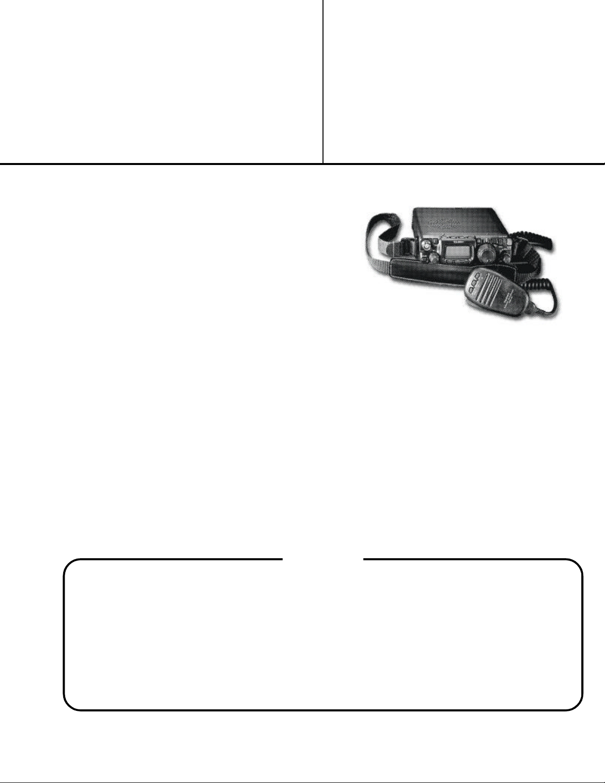
ANTENNA (YHA-63) Q3000174
MIC (MH-31A8J) A06870001
CABLE (E-DC-6) Q9000722 W/O CE
DC CABLE (DC 3A 1500MM) T9023003 W/ CE
Screw List
ACCESSORIES
RA0270100
RUBBER KNOB (CLAR)
RA027150B (Lot.49~)
RA027150A
FRONT PANEL ASSY
RA026960A (Lot.54~)
RA0269600
ROTARY KNOB (SEL)
RA0269700
MAIN KNOB
RA0269800
RUBBER RING
RA0269400
ROTARY KNOB (AF)
RA0283600
REFLECTOR SHEET (A)
RA027160A (Lot. 17~)
RA0271600
LIGHT GUIDE
RA0283700
REFLECTOR SHEET (B)
Q7000291
LCD UNIT
RA0269500
ROTARY KNOB (SQL)
RA027530A
RELEASE KNOB (A)
RA0270200
RUBBER KNOB (MODE)
RA0276300
HOLDER PLATE
RA0271700
LCD HOLDER
*4
*3
R6054387B
SPECIAL NUT
RA0283800
SPONGE RUBBER (SP-A)
M4090150
SPEAKER
RA0270500
SP HOLDER
RA0284300
SPONGE RUBBER (SH-B)
P1091117A (Lot. 17~)
P1091117
CONNECTOR (w/ *1,*2)
RA027540A
RELEASE KNOB (B)
RA027620B
COIL SPRING
(2 pcs)
É
Ä
É
VR UNIT
Q9000709A
ROTARY ENCODER
(W/ *3,*4)
RA027040A (Lot.35~)
RA0270400
RUBBER KNOB (PWR)
RA0293700
SPONGE RUBBER (CASE)
(Lot.23~ W/O CE)
RA0270300
RUBBER KNOB (ABC)
RA0290000
SPONGE RUBBER (BT-B)
RA027090A
BATTERY COVER
*1
PANEL UNIT
Ã
Ã
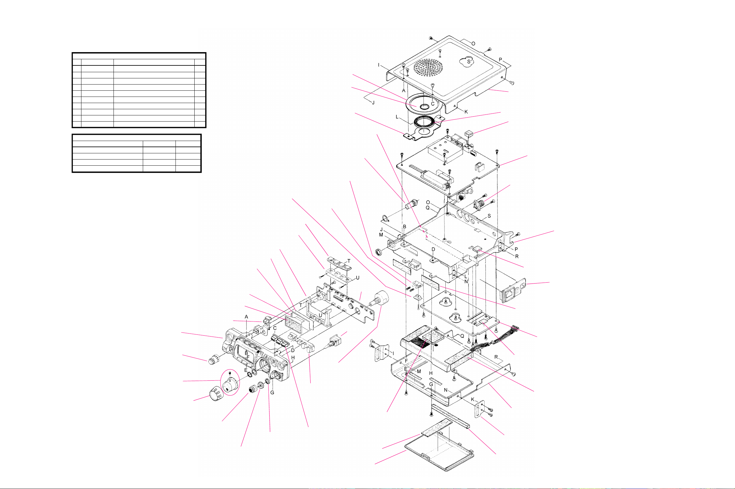
Exploded View & Miscellaneous Parts
È
Á
Ã
È
CP6960001
TOP CASE ASS’Y (W/SP NET)
RA0283900
SPONGE RUBBER (SP-B)
RA031630B (Lot.22~)
RA031630A (10~)
RA0316300 (8~)
RA0293500
SPONGE RUBBER (KEY-F)
Å
P1090352
Æ
CONNECTOR
Æ
Â
RA0284200 (X2 pcs)
SPONGE RUBBER (SH-A)
Å
Á
Ã
RA0293600
PAD
È
Ã
Ã
RA027080A
BOTTOM CASE
RA0276400 (X2 pcs)
BELT HOOK
RA0289900
SPONGE RUBBER (BT-A)
MAIN UNIT
RA026720B (Lot.36~)
RA026720A
CHASSIS
RA0250800
PAD
RA027660A
CONNECTOR COVER
PA UNIT / FINAL UNIT
AAB33X001
FBA-28
3
Ç
È
Ç
È
Å
Å
Å
Å
*2
À
Å
Å
È
Å
Å
Å
Ã
È
È

Exploded View & Miscellaneous Parts
DESCRIPTION VALUE V/W TOL. VS P/NMFR’S DESIG VERS.REF. LOT. SIDE
*** MAIN ASSY ***
P 0004 WIRE ASSY J1012 to SP T9206744 1P 0005 WIRE ASSY J1008 to J4002 T9206919 1P 0006 WIRE ASSY J1003 to J3004 T9206920 1P 0007 WIRE ASSY BATTERY CASE T9206940 1P 0007 WIRE ASSY BATTERY CASE T9206932A 3-
4
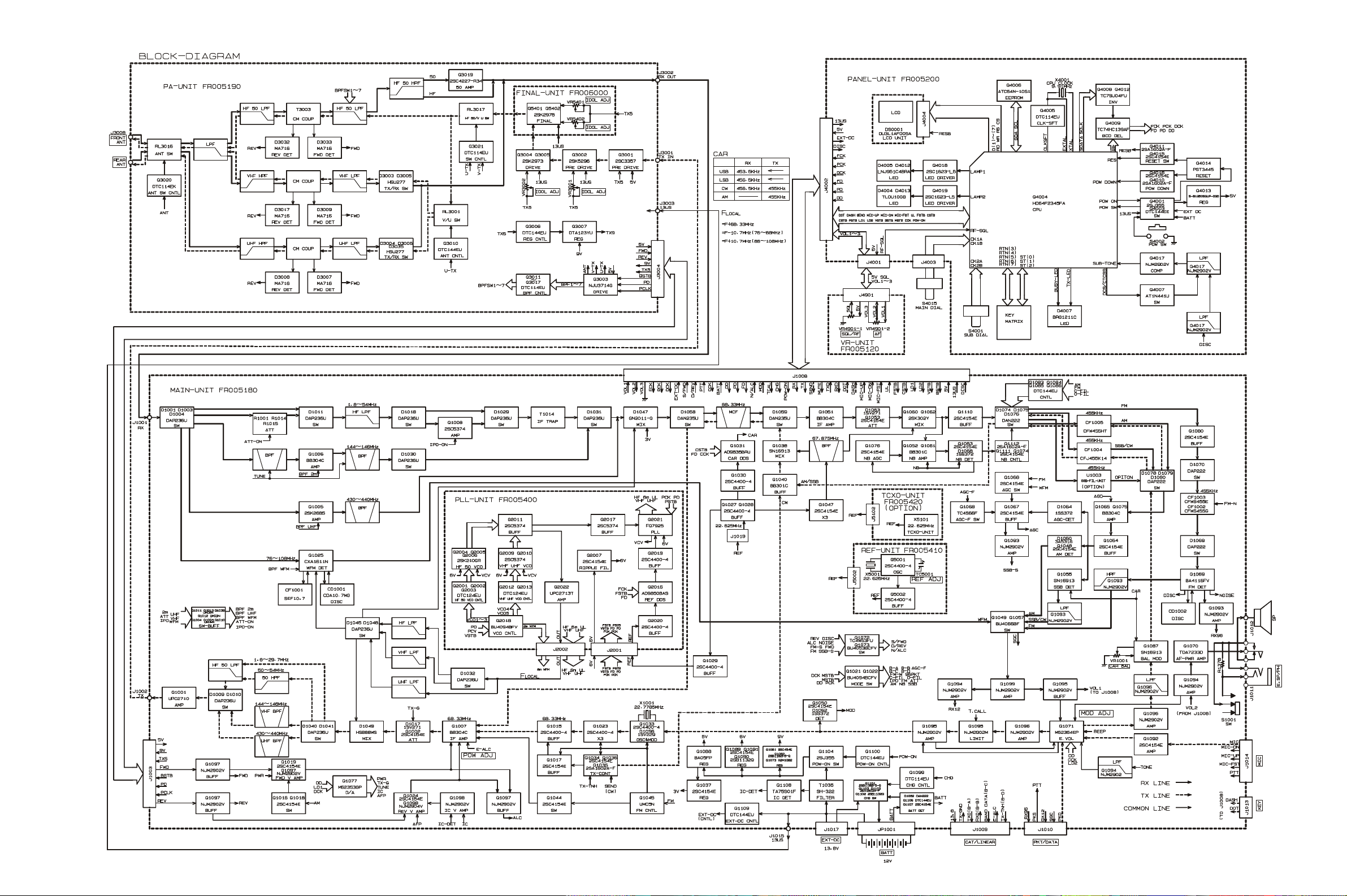
Block Diagram
5

Block Diagram
Note:
6

Circuit Description
The FT-817 internal assembly consists of the MAIN Unit,
Control ( PANEL) Unit, and the PA Unit. The MAIN Unit
contains the receiver front end, PLL IC, and switching circuits, as well as the VCO Unit (local oscillator for transmission and reception). The PANEL Unit contains the
CPU and reset circuits, as well as the power circuitry for
the LCD.
Receive Signal Circuitry
High-Frequency Circuit
The receive signal enters from the Front (J1001) or Rear
(J1002) ANT connector , as selected by relay RL3016 on
the PA Unit.
Signals between 0.1 and 154 MHz received at the antenna terminal pass through an input low-pass filter composed of L3081, L3082, C3264, and C3265.
Received 430 MHz signals, after passing through a highpass filter composed of L3071, L3076, C3245, and C3254
are passed through low-pass filter composed of L3028,
L3032, L3035, C076, C3082, C3088, and C3093, and then
are fed through the directional coupler to the UHF T/R
switch circuit composed of diode switch D3004/D3035
(both HSU277). The signal then is fed to MAIN Unit via
J3002.
Received 145 MHz signals, after passing through a highpass filter composed of L3071, L3075, L3079, C3234, C3245,
C3252, and C3260 are passed through low-pass filter composed of L3027, L3031, L3034, C3075, C3081, and C3092,
and then are fed through the directional coupler to the
VHF T/R switch circuit, composed of diode switch D3003/
D3005 (both HSU277) . The signal then is fed to MAIN
Unit via J3002.
Received 0.1-54 MHz signals, after passing through the
first low-pass filter, are passed through another low-pass
filter composed of L3069, L3070, L3074, L3077, C3239,
C3242, and C3248, plus LPFs 1-7 (5th or 7th-order
Chebyschev type filter) and HPFs 1-7, utilizing seven different sections to create optimized bandpass responses for
the various amateur bands at 0.1-54 MHz. The signal then
is fed to the 50MHz pre-amplifier (when engaged) and on
to the MAIN Unit via J3002.
The receive signal then passes through the input attenuator (-10dB) which consists of resistors R1001, R1014, and
R1015 plus diodes D1003/D1011 (both DAP236U) on the
MAIN Unit .
Incoming wideband FM (76-108 MHz) signals, after passing through a high-pass filter composed of L3071, L3075,
L3079, C3234, C3245, C3252, and C3260 are passed
through a low-pass filter composed of L3027, L3031,
L3034, C3075, C3081, and C3092 , and through a directional coupler, to the VHF T/R switch circuit, composed
of diode switch D3003/D3005 (both HSU277) . Then it is
fed to the MAIN Unit via J3002. The signal is delivered to
IC Q1025 (CXA1611N) which contains the front-end and
discriminator circuits for Wide-FM demodulation. Then
the audio signal is passed to analog switch IC Q1049
(BU4066BF).
The FT-817 includes four receiver front ends, each optimized for a particular frequency range and mode combination.
1st Mixer Circuit/1st IF Circuit
The 1st mixer on the MAIN Unit consists of a quad MES
FET, D1047 (GN2011). The 1st local signal (68.430-538.330
MHz) from the PLL Unit is applied to the gates of each
FET in the 1st mixer.
The resulting output signal (the difference between the
local signal and receive signal) passes through a monolithic crystal filter (MCF) XF1001 (MF68R, BW:±7.5 kHz)
to obtain the 1st IF signal having a center frequency of
68.33 MHz. The signal is then fed to the 2nd mixer circuit
on the MAIN Unit after it is amplified by FET Q1051
(BB304C).
2nd Mixer Circuit/2nd IF Circuit
The 2nd mixer consists of FETs Q1060 and Q1062 (both
2SK302Y) on the MAIN Unit. The 2nd local signal (67.875
MHz) is amplified by Q1047 (2SC4154E) and is applied
to each FET's gate in the 2nd mixer.
The signal output from the 2nd mixer passes through a
ceramic filter, or optional mechanical filter (U1003), to
become the 455-kHz 3rd IF signal.
Noise Blanker Circuit
A sample of the 2nd IF circuit is amplified by FETs Q1052
and Q1061 (both BB301C) on the MAIN Unit, and then
is rectified by D1068 (1SS372). The resulting DC voltage
passes through R1343 and R1345, C1360 and C1362, and
Q1076 (2SC4154E) to yield an average AGC voltage for
7

Circuit Description
controlling the amplification gain of the above FETs. Noise
pulses contained in the output from D1075 are detected
by Q1074 (2SC4154E) and are used to control the NB Gate.
AGC Circuit
The AGC circuit consists of D1064 (1SS372), transistor
Q1066 (2SC4154E), and associated parts on the MAIN
Unit. Output from the AGC circuit is fed back to the RF
and IF stages, controlling their gain levels.
FM IF Circuit/FM Demodulator Circuit
The 2nd IF signal is fed to IC Q1069 (BA4116FV) for FM
demodulation.
The FM demodulator IC contains a mixer, limiter amplifier, filter amplifier, squelch trigger, and demodulator. The
IF input signal is band-limited by ceramic filter CD1002
(CDBC455CX24, BW:±4 kHz), amplified by the limiter
amplifier, and demodulated into an audio signal by the
demodulator; it then passes through a filter (R1308 and
C1293). The signal next passes through a de-emphasis circuit which consists of R1256 and C1286.
The squelch circuit selectively amplifies the noise component of the demodulator output using the filter amplifier inside the FM IC and the active band-pass filter consisting of an externally attached resistor and capacitor. This
circuit uses a signal detected by D1065 (DA221).
SSB/CW Demodulator Circuit
The 2nd IF signal is applied to the SSB demodulator Q1055
(SN16913) on the MAIN Unit, which produces audio by
applying a carrier signal from the CAR-DDS IC (Q1031).
Similarly, the CW signal is demodulated using a carrier
signal which is offset by the "Pitch" frequency.
The demodulated SSB and CW signals are each stripped
of high-frequency components by an active low-pass filter which consists of op-amp IC Q1093-1 (NJM2902V).
Then, they enter the VR Unit via J1008.
AM Demodulator Circuit
The 2nd IF signal from the IF Unit is applied to diode
D1060 (BAS316) for AM demodulation .
volume control VR4901, and IC Q1070 (TDA7233D) to
drive the internal or external speaker with a maximum
output of approximately 1.0 Watt.
Transmit Signal Circuitry
Microphone Amplifier Circuit
The audio signal from microphone jack J1014 on the
MAIN Unit is amplified by transistor Q1092 (2SC4154E)
on the MAIN Unit, and then is applied to electronic volume IC Q1071 (M62364EP), which is controlled via the
User Menu (Item #46: SSB MIC).
The output (audio signal) from the electronic volume IC
is amplified by Q1096 (NJM2902V) and fed to balanced
modulator IC Q1087 (SN16913) through the low-pass filter IC Q1096 (NJM2902V).
During FM transmission, the audio signal is adjusted via
the User Menu (Item# 29 : FM MIC) . The audio signal
that has passed through the pre-emphasis circuit (C2201
and R2228 on the MAIN Unit) may be mixed with a tone
signal from CPU IC Q4004, and is then amplified and limited by op-amp IC Q1095-4 (NJM2902V) of the IDC circuit. The audio then passes through the splatter filter (secondary active low-pass filter) formed by op-amp IC
Q1095-1 (NJM2902V), R1321, and R1322, plus C1344, and
is then fed to the frequency-modulator circuit on the
MAIN Unit through R1183 and R1477 for setting of the
frequency deviation.
SSB Modulator Circuit
The carrier signal appropriate to the transmitting mode
(LSB or USB) is applied from the CAR-DDS Unit to balanced modulator IC Q1087 (SN16913) on the MAIN Unit,
and is modulated by microphone audio.
The balanced modulator produces the upper and lower
side bands and carrier signal. The carrier and audio signal are suppressed and the carrier balance is adjusted by
VR1001. As a result, the output signal obtained is a DSB
signal with a carrier suppression of 30 dB or more (additional carrier suppression is supplied by the SSB filter).
The output from the detector passes through analog switch
Q1049 (BU4066BF). Then, it enters the VR Unit via J1008.
Audio Amplifier Circuit
The demodulated signal that is selected by one of analog
switches IC Q1057 (according to the reception mode)
passes through the audio amplifier IC Q1094 (NJM2902V),
8
The DSB modulated signal (1st IF signal: 455 kHz) then
passes through ceramic filter CF1004 (CFJ455K14) or the
optional mechanical filter U1003 on the MAIN Unit, stripping residual carrier and the undesired sideband; the signal then passes as an SSB signal through buffer-amplifier
Q1040 (BB301C).

Circuit Description
AM Modulator Circuit
As in the SSB modulator circuit, a carrier signal from the
CAR-DDS Unit and an audio signal from the microphone
are applied to balanced modulator IC Q1087 (SN16913)
on the MAIN Unit.
The control signal from MODE SW IC Q1021
(BU4094BCFV) on the MAIN Unit causes a voltage labeled
"AM 5V" to be sent from transistor Q1079 (2SC4154E). This
voltage is applied to IC Q1087 via D1077 (BAS316), causing the balanced modulator to lose balance. The restored
carrier signal and modulated signal are then fed to the Tx
mixer via ceramic filter CF1004 (CFJ455K14) on the MAIN
Unit.
Frequency Modulation Circuit
The FM circuit uses a voltage controlled crystal oscillator
(VCXO) which consists mainly of Q1033 (2SC4400),
X1001 on the MAIN-Unit, varactor diode D1056
(HVC362), and T1018. The VCXO has a center frequency
of 22.7785MHz.
The FM signal is produced by applying a signal from the
FM microphone amplifier circuit to varactor diode D1056
and varying the crystal oscillator load capacity in proportion to the signal voltage.
CW (A1) Signal Generator Circuit
When the transmitting mode is CW (A1), the control signal from D-A converter IC Q1077 (M62353GP) on the
MAIN Unit creates a "CW 5V" voltage. The voltage is
applied to balanced modulator IC Q1087 via D1071, providing a carrier from the balanced modulator for the input to the transmit signal circuit of the MAIN Unit.
1st IF Circuit/1st Mixer Circuit
The 455 kHz 1st IF signal from the modulator circuit is
band-limited by the MAIN Unit's ceramic (CF1004) or
optional mechanical filter U1003 (XF5201 or XF5301) according to the selected mode (CW, SSB, or AM). It is then
buffer-amplified by FET Q1040 (BB301C) and fed to 1st
mixer IC Q1038 (SN16913).
The IF Unit's double balanced mixer IC Q1038 (DBM) is
used as the 1st mixer. A local signal (67.875MHz) is produced by tripling the Reference frequency at Q1047
(2SC4154E), and this local signal is fed to the "local" port
of the doubly-balanced mixer IC, where it is mixed with
the 455 kHz 1st IF signal to produce a 68.33MHz 2nd IF
signal.
2nd IF Circuit/2nd Mixer Circuit
The 2nd IF signal passes through crystal filter XF1001
and then is fed to the 2nd mixer circuit.
The 2nd mixer consists of the MAIN Unit's D1049
(HSB88WS). The 2nd local signal (68.430-538.330MHz)
from the PLL Unit is applied to the gates of each FET in
the 2nd mixer.
High-Frequency Transmit Preamplifier Circuit
The transmit signal is passed through a low-pass filter (1.8-
29.7 MHz), a high-pass filter (50-54 MHz), a band-pass
filter (144-146 MHz), or a band-pass filter (430-440 MHz)
and then is amplified by Q1001 (UPC2710), and passed
onward to the PA Unit via J1002.
Power Amplifier Circuit
The transmit signal from the MAIN Unit arrives at connector J3001 on the PA Unit.
The transmit signal (1.8 MHz to 430 MHz) delivered to
the PA Unit is amplified by pre-driver Q3001 (2SC3357),
driver Q3002 (2SK5296) and final amplifiers Q5401/Q5402
(2SK2975).
Low-Pass Filter (LPF) Circuit
The transmission signal from the power amplifier circuit
is passed through a low-pass filter which consist mainly
of RL3001-RL3015, RL3017, and corresponding inductor
and capacitor networks. The LPF is a 5th or 7th-order
Chebyschev type filter, utilizing nine different sections for
the various amateur bands at 1.8 ~ 430 MHz.
The low-pass filtered transmission signal is fed to the
FRONT ANT connector (J0001) or REAR ANT connector
(J0002) through the triplexer and directional coupler.
The directional coupler samples a part of the transmission power to detect forward power and reflected power.
A DC voltage corresponding to the relative forward/reflected power is produced by D3032/D3033 (both MA716,
1.8 to 54 MHz), D3009/D3017 (both MA716, 144 to 148
MHz), or D3007/D3008 (both MA716, 430 to 450 MHz) ,
and is used for automatic level control (ALC).
ALC Circuit
The output from the directional coupler is routed from
connector J3004 and applied to the ALC circuit via connector J1003 on the MAIN Unit.
The ALC circuit consists of an op-amplifier circuit for
amplifying the forward and reflected voltage, a time-con-
9

Circuit Description
stant ALC amplifier, and a transmit signal control circuit
on the MAIN Unit.
The forward voltage from connector J1003 on the MAIN
Unit is added with a DC control voltage and is then applied to op-amp IC Q1097 (NJM2902V).
The reflected voltage is added with a DC control voltage
and is then applied to op-amp IC Q1098 (NJM2904V), In
the event of high SWR conditions (SWR of 3:1 or more),
transmitter output is reduced and a "High SWR" warning appears, thus protecting the PA Unit from potential
damage and alerting the operator to the high SWR situation.
The ALC amplifier amplifies the "forward" DC output via
transistor Q1019 (2SC4154). This output then passes
through a fast-attack, slow-delay RC time-constant circuit
which consists of R1097 and C1113 for the input to the Tx
signal control circuit on the MAIN Unit.
The TX control circuit adjusts the IF amplifier gain via
gate 2 of FET Q1007 (BB304C) of the 68.33 MHz IF amplifier circuit to prevent the power output from exceeding
the preset level.
PLL Frequency Synthesizer
The PLL Frequency Synthesizer consists mainly of a master reference oscillator circuit, 2nd local oscillator circuit,
plus the PLL IC, CAR-DDS, and REF-DDS units, which
digitally synthesize carrier outputs, and a PLL circuit
which contains a voltage controlled oscillator (VCO).
Master Reference Oscillator Circuit
The master reference oscillator uses a crystal oscillator
(oscillation frequency: 22.625MHz) composed of Q5001
(2SC4400-4), X5001, TC5001, C5001, R5005, and associated
components. The reference oscillator signal passes through
buffer amplifier Q5002 (2SC4400-4), C5004, C5007, R5003,
R5004, R5007, and is then fed to the MAIN Unit via J5002.
CAR-DDS Circuit /REF-DDS Circuit
DDS ICs Q1031 (AD9835BRU) and Q2016 (AD9850BAS)
each contain a shift register, selector, phase accumulator,
and ROM.
The reference oscillation frequency (22.625MHz) that is
delivered to each of the DDS Units is applied to each DDS
IC after amplification by transistors Q1028/Q2020 (both
2SC4400-4).
The DDS outputs contain digital amplitude data corresponding to serial frequency data from CPU IC Q4004 of
the PANEL Unit. The DDS frequency range is 453.5 ~ 466.5
kHz (cf = 455.0 kHz) for the CAR-DDS, and 7.2-8.0 MHz
for the REF DDS.
2nd Local Oscillator Circuit
The 2nd L.O. circuit is a Hartley-type overtone oscillator
circuit (frequency: 67.875 MHz) composed of Q1047
(2SC4400) on the MAIN Unit.
1st Local Oscillator Circuit
VCO output is buffer-amplified by Q2008 (2SC4400),
Q2011, Q2014, and Q2016(all 2SC5374) and passes
through a low-pass filter. It is then fed to the Tx/Rx frequency mixer circuitry on the MAIN Unit.
PLL Circuit
The PLL circuit is a frequency mixing type composed of a
VCO, mixer, PLL IC, and loop filter.
The VCO consists of five circuits (VCO1, VCO2, VCO3,
VCO4, and VCO5), with a frequency range of 68.430-
538.330 MHz divided into five bands, allocated to the five
VCO circuits. VCO1-VCO5 consist mainly of FETs Q2004,
Q2005, and Q2006 (all 2SK210GR), transistors Q2009,
Q2010 (both 2SC5374), diodes D2001-D2006 (all HVC362),
D2007 (1SV282), D2008 (1SV281), and D2009 (1SV286), and
coils T2001-T2003, L2010, and L2011.
The VCO switching signal from connector J2002 is used
to drive switching transistors Q2001, Q2002, Q2003,
Q2012, and Q2013 (all DTC124EU) to switch the source
terminal of the oscillator FET.
The 68.430-538.330 MHz VCO signal is fed to mixer D1047
(GN2011-Q).
The REF-DDS signal (7.2-8.0 MHz) is fed to PLL IC Q2022
(FQ7925) after it passes through a LPF composed of C2064,
C2067, C2069, C2071, C2075, L2014, L2015, and L2016 ,
and buffer amplifier Q2019 (2SC4400-4) .
The phase of the reference frequency and that of the signal input to PLL IC are compared, and a signal whose
pulse corresponds to the phase difference is produced.
The VCO frequency is controlled by a first lag filter which
consists of R2057, R2065, R2062, and C2090 and a secondary lag filter composed of C2085, C2088, and R2053.
10

Circuit Description
Control Circuitry
Microprocessor Circuit
The microprocessor circuit, which is composed of CPU
IC Q4004 (HD64F2345) and EEPROM IC Q4004 (ATC64N10S1), performs various types of processing, such as control signals, serial I/O, A/D conversion, dial counter circuit control, key input, and display functions.
The EEPROM memorizes various parameters and settings
(transmission frequency range, transmission output control) and carrier points according to the transceiver version and the contents of memory channels.
Reset Circuit
The reset circuit consists mainly of PANEL Unit ICs Q4014
(PST3445), Q4015 (2SC4154E), Q4011 (2SA1602A), Q4016
(2SC4154E), and Q4010 (2SA1602A), and associated capacitors and resistors. This circuit controls the powerdown input port, CPU reset input, keyer CPU, and related circuits.
Dial Counter Circuit
The dial counter circuit consists of Main Dial and SEL (Selector) Knob. This circuit detects a two-phase pulse having a phase difference of 90 degrees and delivers it to CPU
IC Q4006 .
Serial Data Communication Circuit
The Serial Data Communication Circuit consists of ICs
Q4008, Q4009, Q4010, etc. on the PANEL-Unit. These ICs
distribute a set of serial data (Data/Clock/Strobe) generated by CPU to various devices, such as CAR-DDS, REFDDS, E.VOL, D/A, or Shift-Register for controlling analog switching , band switching, VCO selection, etc. Serial
data communication is clock synchronous for the above
purposes, whereas the serial data is transferred to an asynchronous signal for the CAT system for external computer
control of the transceiver).
this circuit reads the input data for processing by the CPU.
Analog-Digital Converter Circuitry
Forward and reflected voltage, ALC, DISC, S-meter, etc.
metering options are selected by MAIN Unit IC Q1073
(BU4053BCF) and are fed to the A/D port of CPU IC Q4004
for conversion into digital values to be processed prior to
display on the LCD. The individual voltages, converted
into digital values, are displayed as PO, SWR, ALC, VCC,
and S-meter indications on the LCD panel.
LED Drive Circuit
The LED drive circuit consists of PANEL Unit transistors
Q4018 and Q4019 (both 2SC1623) and the LEDs. This circuitry drives (turns on/off) the appropriate LEDs.
LCD Circuit
Data processed by the CPU IC is sent as parallel data to
LCD Unit DS4001 .
CTCSS Tone Generator Circuit
The CTCSS tone generator circuit consists mainly of CPU
IC Q4004 and active filter IC Q1094 (NJM2902).
Electronic Keyer Circuit
The electronic keyer circuit consists of CPU IC Q4004.
When the CW mode is selected, this circuit controls the
generation of Morse characters.
Various types of data, such as operating frequency, mode,
and display data, are processed by CPU IC Q4004 .
The CAT (external computer control) signals are converted
to RS232 interface standard levels by the optional CAT
Interface Cable (CT-62).
Key Matrix Circuit
The key matrix circuit consists of PANEL Unit diodes
D4001-D4003 and D4006 (all IMN10) and the panel key
switches arranged on the matrix. When a key is pressed,
11

Circuit Description
Note:
12

Alignment
Introduction
The FT-817 has been carefully aligned at the factory for
the specified performance across the amateur band. Realignment should therefore not be necessary except in the
event of a component failure. All component replacement
and service should be performed only by an authorized
VERTEX STANDARD representative, or the warranty
policy may be voided.
The following procedures cover the sometimes critical and
tedious adjustments that are not normally required once
the transceiver has left the factory. However, if damage
occurs and some parts are replaced, realignment may be
required. If a sudden problem occurs during normal operation, it is likely due to component failure; realignment
should not be done until after the faulty component has
been replaced.
We recommend that servicing be performed only by authorized VERTEX STANDARD service technicians who are experienced with the circuitry and fully equipped for repair
and alignment. Therefore, if a fault is suspected, contact the
dealer from whom the transceiver was purchased for instructions regarding repair. Authorized VERTEX STANDARD service technicians realign all circuits and make complete performance checks to ensure compliance with factory specifications after replacing any faulty components.
Those who do undertake any of the following alignments
are cautioned to proceed at their own risk. Problems caused
by unauthorized attempts at realignment are not covered
by the warranty policy. Also, VERTEX STANDARD must
reserve the right to change circuits and alignment procedures in the interest of improved performance, without
notifying owners. Under no circumstances should any alignment be attempted unless the normal function and operation of the transceiver are clearly understood, the cause of
the malfunction has been clearly pinpointed and any faulty
components replaced, and the need for realignment determined to be absolutely necessary.
Required Test Equipment
The following test equipment (and thorough familiarity
with its correct use) is necessary for complete realignment.
Correction of problems caused by misalignment resulting from use of improper test equipment is not covered
under the warranty policy. While most steps do not require all of the equipment listed, the interactions of some
adjustments may require that more complex adjustments
be performed afterwards. Do not attempt to perform only
a single step unless it is clearly isolated electrically from
all other steps. Have all test equipment ready before beginning, and follow all of the steps in a section in the order presented.
r RF Signal Generator with calibrated output level at 500
MHz
r Deviation Meter (linear detector)
r AC Voltmeter
r SINAD Meter
r Inline Wattmeter with 5% accuracy at 500 MHz
r Regulated DC Power Supply: adjustable from 8 to 16.5
VDC, 5A
r 50-Ohm Non-reactive Dummy Load: 5 W at 500 MHz
r 150-Ohm Dummy Load: 5 W at 500 MHz
r FM Linear Detector
r Frequency Counter: ±0.1 ppm accuracy at 500 MHz
r AF Signal Generator
r DC Voltmeter: high impedance
r VHF Sampling Coupler
r AF Dummy Load: 4 Ohms, 5 W
Alignment Preparation & Precautions
A dummy load and inline wattmeter must be connected
to the main antenna jack in all procedures that call for
transmission, except where specified otherwise. Correct
alignment is not possible with an antenna. After completing one step, read the following step to determine whether
the same test equipment will be required. If not, remove
the test equipment (except dummy load and wattmeter, if
connected) before proceeding.
Correct alignment requires that the ambient temperature
in the repair shop be the same as that of the transceiver
and test equipment, and that this temperature be held
constant between 20° and 30°C (68° ~ 86°F). When the
transceiver is brought into the shop from hot or cold air it
should be allowed some time for thermal equalization with
the environment before alignment. If possible, alignments
should be made with oscillator shields and circuit boards
firmly affixed in place. Also, the test equipment must be
thoroughly warmed up before beginning.
13
Alignment
The alignment procedure for the FT-817 involves several
steps requiring that the case be opened to gain access to
the components to be adjusted. These procedures are described first in the pages to follow. A number of alignment categories, however, may be accomplished without
opening the transceiver case, utilizing the Alignment
Menu feature which allows adjustments to be accomplished using the front panel controls.
Please survey the pages to follow. Depending on the
problem(s) needing correction, you may be able to skip to
the software-based alignment section.
Use external DC input of +13.8 Volts via the rear panel
DC input jack, for all alignment steps.
Local Oscillator Adjustment
Reference Frequency Adjustment
1. Connect the frequency counter to Q1038 (pin 5).
2. Adjust trimmer capacitor TC5001 (on the REF-Unit) for
a reading of 67.875 MHz (±10 Hz) on the frequency
counter.
3. Connect the RF millivoltmeter or an oscilloscope to
J5002 (pin 2) and confirm that the output level is at least
60 mVrms or 169 mVp-p.
PLL Adjustment
VCO VCV Adjustment
Connect the DC voltmeter to J2002 (pin 6) and referring
to the table below, tune the transceiver to each frequency
listed. Then confirm that the correct voltage is present, or
adjust the listed components for the required voltage.
Tune to : Adjust / Confirm For
13.895 MHz, CW mode Adjust T2001 4.6 V ±0.2 V
76.000 MHz, CW mode Confirm At least 0.5 V
29.995 MHz, CW mode Adjust T2002 4.2 V ±0.2 V
13.900 MHz, CW mode Confirm At least 0.8 V
53.995 MHz, CW mode Adjust T2003 4.4 V ±0.2 V
88.000 MHz, CW mode Confirm At least 0.8 V
146.000 MHz, CW mode Adjust L2010 3.8 V ±0.2 V
144.000 MHz, CW mode Confirm At least 3.0 V
440.000 MHz, CW mode Adjust L2011 2.4 V ±0.2 V
430.000 MHz, CW mode Confirm At least 1.0 V
Q1038 (pin 5)
T2003
T2002
L2010
T2001
TC5001
J5002 (Pin 2
)
J2002 (Pin 11
J2002 (Pin 6
L2011
J2002 (Pin 1
)
)
)
14
Alignment
1st Local Output Level
1. Connect the RF millivoltmeter to J2002 (pin 11) and tune
the transceiver to 28.000 MHz in the CW mode.
2. Confirm that the RF level is at least +5 dBm (or 400
mVrms).
PLL "Unlock" Display Alert
1. Connect the DC voltmeter to J2002 (pin 1).
2. Disconnect the 4-pin plug connected to J5002 (REF-Unit),
and confirm that (A) the voltmeter shows less than 0.5 V
and (B) that "UNLOCK" is displayed on the LCD.
3. Re-connect the 4-pin plug to J5002, and confirm that
the voltmeter shows at least 3.5 V and that LCD display has returned to normal.
PA Unit Adjustment
Before alignment, set the mode to CW and tune the transceiver to 1.800 MHz. Nothing should be connected to the
CW Key Jack.
5. Press the PTT switch, and adjust VR3002 for an indica-
tion of 20 mA (±2 mA) on the ammeter.
6. Disconnect the ammeter and reinstall the jumper con-
nector at J3006.
Final Stage Idling Current
1. Connect the ammeter between the "13US" pin on PA
Unit and the "13US" pin of the Final Unit. The "13US"
line is currently connected by a wire; remove it so you
can connect the ammeter.
2. Turn both VR5401 and VR5402 fully counterclockwise.
3. Press the PTT switch, and adjust VR5401 for an indication of 45 mA (±2 mA) on the ammeter.
4. Press the PTT switch, and adjust VR5402 for an indication of 76 mA (±4 mA) on the ammeter.
5. Release the PTT switch. Re-connect the "13US" line between PA unit and Final Unit.
Driver Stage Idling Current
1. Remove the jumper connector at J3005, and insert an
ammeter in its place.
2. Press the microphone's PTT switch, and adjust VR3001
for an indication of 30 mA (±2 mA) on the ammeter.
3. Disconnect the ammeter and reinstall the jumper con-
nector at J3005
4. Remove the jumper connector at J3006 and insert the
ammeter in its place.
VR5401
VR5402
VR3002
J3006
VR3001
J3005
Jumper
15

Alignment
Local Oscillator Adjustment
2nd Local Adjustment
1. Connect the RF millivoltmeter or an oscilloscope to
Q1038 (pin 5).
2. Adjust T1024 and T1026 alternately for maximum in-
dication on the millivoltmeter or for maximum amplitude on the oscilloscope.
3. Confirm the indicated voltage is at least 120 mVrms or
330 mVp-p.
3rd Local Adjustment
1. Connect the RF millivoltmeter or an oscilloscope to pin
5 of Q1055.
2. Key the transceiver in the CW mode, and adjust T1021
for maximum indication on the RF millivoltmeter.
3. Confirm that the indicated voltage is at least 70 mVrms
or 200 mVp-p.
TX IF Adjustment
CW TX IF Adjustment
1. Tune the frequency to 1.8 MHz in the CW mode. Connect the RF millivoltmeter to J1002, terminated by a 50
Ohm dummy load.
2. Key the transceiver, and adjust T1020, T1012, and T1005
alternately for maximum indication on the RF
millivoltmeter.
FM TX IF Adjustment
1. Tune the frequency to the 29 MHz band in the FM mode.
Leave the RF millivoltmeter connected to J1002, still
terminated by the 50 Ohm dummy load.
2. Key the transceiver, and adjust T1012 and T1013 alternately for the maximum indication on the RF
millivoltmeter.
3. Connect the frequency counter to T1022 (pin 5).
4. Again key the transceiver in the FM mode (without
microphone audio input). Adjust T1018 for a reading
of 68.3300 MHz (±50 Hz).
Carrier Balance Adjustment
1. Terminate J1002 with a 50 Ohm dummy load, and connect a spectrum analyzer or a RF millivoltmeter to J1002.
2. Key the transceiver in the USB mode on the 28 MHz
band (without microphone input). Adjust VR1001 for
the maximum carrier suppression on the spectrum analyzer, or for the minimum indication on the RF
millivoltmeter.
VHF TX BPF Adjustment
1. Set the frequency at 145.995 MHz. Connect the RF
millivoltmeter to J1002 terminated by a 50ohm dummy load.
2. Key the transceiver on FM mode and adjust T1011,
T1010, and T1009 alternately for the maximum indication on RF millivoltmeter.
UHF TX BPF Adjustment
1. Set the frequency to 439.995 MHz. Connect the RF
millivoltmeter to J1002, which still should be terminated by the 50 Ohm dummy load.
2. Key the transceiver in the FM mode, and adjust TC1005,
TC1004 and TC1002 alternately for maximum indication on the RF millivoltmeter.
RX Adjustment
The PA Unit must be connected during RX adjustment.
Note that the signal generator should not be connected to
J1008 (pin 15) because DC voltage is present there.
RX IF Adjustments
Connect the signal generator to the antenna connector, and
a SINAD meter to the speaker jack.
SSB IF Adjustment
1. Connect the DC voltmeter to J1008 (pin 15).
2. Tune the transceiver to 51.995 MHz. Inject an RF signal
from the signal generator at a level of 40 dBµ.
3. Adjust T1033, and T1029 alternately for the minimum
indication on the DC voltmeter.
4. Now select the FM mode. Turn off the RF injection from
the signal generator output.
5. Adjust T1034 for maximum indication on the DC voltmeter.
FM IF Adjustment
1. Tune the transceiver to 51.995 MHz. Inject an RF signal
from the signal generator at a level of 10 dBµ, with 1
kHz of FM modulation at ±3.5 kHz deviation.
2. Adjust T1023, T1025, T1028, T1030 and T1034 alternately for the best SINAD sensitivity.
VHF Band Alignment
1. Connect the DC voltmeter to J1008 (pin 15).
2. Tune the transceiver to 145.995 MHz. Inject an RF signal from the signal generator at a level of 40dBµ.
3. Adjust T1002, T1004, and T1008 alternately for the
minimum indication on the DC voltmeter.
16
Alignment
UHF Band Alignment
1. Connect the DC voltmeter to J1008 (pin 15).
2. Tune the transceiver to 439.995 MHz. Inject an RF signal from the signal generator at a level of 40dBµ.
3. Adjust TC1001 for minimum indication on the DC voltmeter.
W-FM Reception Adjustment
1. Connect a SINAD meter to the speaker jack.
2. Tune the transceiver to 88.000 MHz. Inject an RF signal
from a signal generator at a level of 30dBµ, with
±22.5KHz deviation of a 1 kHz audio tone.
3. Adjust TC1003 for the best SINAD sensitivity. Then reduce the output level of the signal generator and adjust TC1003 again, as minor improvements of SINAD
may be difficult to observe if the SINAD reading is high.
Image Rejection Trap Adjustment
1. Connect the AF millivoltmeter to the speaker jack.
2. Tune the transceiver to 51.995 MHz in the CW mode.
Inject an RF signal from the signal generator at 68.330
MHz, with 50dBµ output.
3. Adjust T1014 for minimum indication on the AF
millivoltmeter. Then increase the output level of the
signal generator slightly, and adjust T1014 again (to
ensure maximum rejection).
Noise Blanker Adjustment
1. Connect the DC voltmeter to the base of Q1074. Tune
the transceiver to 51.995 MHz, and inject an RF signal
from the signal generator at a level of 6 dBµ.
2. Activate the noise blanker, and adjust T1027 for mini-
mum indication on the DC voltmeter.
T1005
T1012
T1013
T1018
T1022 (Pin 5
T1011
T1014
T1023
T1021
T1025
Q1038 (Pin 5
T1024
T1026
T1020
VR1001
Q1055 (Pin 5
T1029
J1008 (Pin 15
TC1003
TC1005
TC1004
TC1002
)
)
)
)
J1002
T1009
T1010
T1008
T1004
TC1001
T1002
T1028
T1030
T1027
Q1074 (Base
T1034
T1033
)
17
Alignment
CM Coupler Balance Adjustment
1. Terminate the antenna jack with a 50 Ohm dummy load.
Set the mode to CW, and connect the DC voltmeter to
J3004 (pin 7).
2. Tune the transceiver to 28.000 MHz, and key the transceiver.
3. Adjust TC3003 for minimum indication on the DC voltmeter.
4. Tune the transceiver to 145.995 MHz (CW), and key
the transceiver.
5. Adjust TC3001 for minimum indication on the DC voltmeter.
6. Tune the transceiver to 439.995 MHz (CW), and key
the transceiver.
7. Adjust TC3002 for minimum indication on the DC voltmeter.
J3004 (Pin7
)
TC3003
TC3001
TC3002
18
Alignment
Software Menu Alignment
For all the following alignment procedures, the antenna
connector should be connected to a dummy load and
wattmeter in all procedures requiring transmission, and
the signal generator should be connected when receiver
alignment is involved. General alignment conditions are
as follows, unless otherwise noted.
AF-gain knob : Center
RF-gain knob : Fully clockwise
SQL : Fully counterclockwise
ATT / IPO / CTCSS / DCS : Off
Output power : High
AGC : Auto
Break-in : On CW Keyer : Off
VOX : Off
Entering the Alignment Mode
To enter the Alignment Mode, press and hold in the
[A],[B], and [C] keys simultaneously; while holding them
in, turn on the transceiver. Once the transceiver comes on,
you may release the three keys. Now press and hold in
the [F] key for ½ second to activate the Menu, which will
be observed to contain a large number of selections not
normally available during regular Menu operation.
In the alignment procedures to follow, each alignment item is
selected by rotating the SEL knob, while adjustment of the selected alignment parameter is accomplished by rotating the
main dial.. Press the [A] key to "set" certain designated parameters where a signal reading is made by the microprocessor (for
automatic setting of the parameter).
To store the alignment parameters after all items have been adjusted, press the [F] key for at least ½ second; this will cause the
transceiver to save all settings and exit the Menu mode.
RF Gain Adjustment
1. Tune the transceiver to 1.909 MHz (CW mode). Select
"01 HF1RXG" in the Alignment Menu by rotating the
SEL knob. Now inject an RF signal from the signal generator at 1.909 MHz at about 32dBµ output, and peak
the S-meter reading on the incoming signal by rotating
the main dial. When the peak is found, reduce the signal generator level to 12 dBµ.
2. Set the parameter "01 HF1RXG," such that the first dot
of the S-meter (S1) on the LCD is illuminated, by rotating the main dial. Rotating the main dial adjusts the
receiver's IF Gain around 1.9 MHz.
3. The remaining five RF gain adjustment points should
be aligned as shown in steps (1) and (2) above. The
output levels of the signal generator (for one "dot" of
S-meter deflection) at each frequency are shown below.
Frequency Select Menu # Output Level of SG
1.909 MHz 01 HF1RXG 15 dB
7.010 MHz 02 HF2RXG 15 dB
21.105 MHz 03 HF3RXG 12 dB
51.050 MHz 04 50MRXG 3 dB
145.940 MHz 05 VHFRXG 3 dB
440.000 MHz 06 UHFRXG 3 dB
µ
µ
µ
µ
µ
µ
SSB S-Meter Adjustment
1. Tune the transceiver to 21.105 MHz on CW mode. Inject an RF signal from the signal generator at a level of
39dBµ, and peak the S-meter deflection on the incoming signal.
2. Set the parameter "07 SSB-S9" so that exactly 6 dots of
the S-meter (S9) appear on the LCD by rotating the main
dial.
3. Now inject a signal on the same frequency at a level of
86dBµ.
4. Set the Alignment Menu parameter "08 SSB-FS" such
that all the dots of the S-meter on the LCD appear by
rotating the main dial.
FM S-Meter Adjustment
1. Tune the transceiver to 145.940 MHz (FM mode). Inject
an RF signal from the signal generator at a level of -3
dBµ, with ±3.5 kHz deviation of 1 kHz audio tone.
2. Select Alignment Menu item "09 FM-S1," and press the
[A] key to set this parameter.
3. Increase the output level of the signal generator up to
22dBµ. Select Alignment Menu item
"10 FM-FS," and press the [A] key to set this parameter.
FM Center Meter Adjustment
1. Tune the transceiver to 145.937 MHz (FM mode). Inject
an RF signal from the signal generator at a level of
10dBµ, with ±3.5 kHz deviation of a 1 kHz audio tone.
2. Set the frequency of the signal generator to 145.934 MHz
(3 kHz below the receiving frequency of the transceiver). Select Alignment Menu item "11 DISC-L," and
press [A] to set this parameter.
19

Alignment
3. Tune the transceiver to 145.943 MHz (FM mode). leave
the signal generator at 10dBµ output, as before.
4. Set the frequency of the signal generator to 145.946 MHz
(3 kHz above the receiving frequency of the transceiver).
Select Alignment Menu item "12 DISC-H," and press
[A] to set this parameter.
FM Squelch Adjustment
1. Tune the transceiver to 145.940 MHz (FM mode). Confirm that the squelch knob is turned fully counterclockwise.
2. Select Alignment Menu item "13 FM-TH1," and press
the [A] key (without any RF input from the signal generator) to set this parameter.
3. Select Alignment Menu item "14 FM-TH2," and press
the [A] key again.
4. Inject an RF signal from the signal generator at 3 dBµ
output, with ±3.5 kHz deviation FM of a 1 kHz tone.
Select Alignment Menu item "15 FM-TI1," and press
the [A] key to set this parameter. 5. Select Alignment
Menu item "16 FM-TI2," leave the signal generator level
unchanged, and press the [A] key again.
Power Supply Voltage Display Adjustment
1. Tune the transceiver to the 144 MHz band (FM mode).
Confirm that the power supply voltage is 13.8V ±0.1V
(using the DC voltmeter).
2. Select the Alignment Menu item "VCC," and adjust the
parameter so that "138" is displayed on the LCD.
Over-Current Protection Adjustment
1. Select Alignment Menu item "18 HF1-IC." Tune the
transceiver to the 1.8 MHz band (CW mode), and key
the transceiver. Adjust this parameter for 7.0 W of transmission power as measured on the external wattmeter.
2. The over-current protection Alignment Menu items, "19 HF2IC," "20 HF3-IC," "21 50M-IC," "22 VHF-IC," and "23 UHF
IC" should be adjusted in the same manner on the 7 MHz, 21
MHz, 50 MHz, 144 MHz, and 430 MHz bands, respectively.
Use the CW mode, and the precise frequency is not critical.
RF Power Adjustment
1. Tune the transceiver to the 1.8 MHz band (CW mode).
Select Alignment Menu item "24 HF1-HI." Key the
transmitter, and adjust this parameter for 5.0 W (±0.1
W) of output power.
2. Select Alignment Menu item "25 HF1-L3." Key the transmitter, and adjust this parameter for 2.5 W (±0.2 W) of
output power.
3. Select Alignment Menu item "26 HF1-L2". Key down and
adjust the parameter for 1.0W (±0.2W) transmission power.
4. Select the menu item "27 HF1-L1." Key the transmitter,
and adjust this parameter for 0.5 W (±0.1 W) of output
power.
5. Other RF power adjustment menu, designated [HF2**], [HF3-**], [50M-**], [VHF-**], and [UHF-**] (four
adjustments each) should be adjusted in exactly the
same manner on the 7 MHz, 21 MHz, 50 MHz, 144 MHz
and 430 MHz bands, respectively. Use the CW mode,
and the precise frequency is not critical.
TX Gain Adjustment
1. Select the USB mode. Inject a 1 mV audio signal at 1
kHz from the AF generator into the microphone jack
(pin 4).
2. Tune the transceiver to the 1.8 MHz band and key the
transmitter. Select Alignment Menu item "48 HF1TXG,"
and adjust this parameter for 2.5 W (±0.1 W) of output
power. Note: to "key the transmitter" with no microphone connected, you may connect pin 3 of the Mic
jack to ground (pin 2).
3. The other TX gain Alignment Menu selections, designated [49 HF2TXG], [50 HF3TXG], [51 50MTXG], [52
VHFTXG], and [53 UHFTXG,] should be adjusted in
the same manner on the 7 MHz, 21 MHz, 50 MHz, 144
MHz, and 430 MHz bands, respectively.
Power Meter Sensitivity Adjustment
1. Set the mode to CW, and the output power to HIGH.
Select Alignment Menu item "54 HF1POM," and key
the transceiver.
2. Set this parameter such that 8 dots of the power meter
scale are displayed on the LCD.
3. The other power meter sensitivity Alignment Menu selections, designated [55 HF2POM], [56 HF3POM], [57
50MPOM], [58 VHFPOM], and [59 UHFPOM], should
be adjusted in the same manner on the 7 MHz, 21 MHz,
50 MHz, 144 MHz, and 430MHz bands, respectively. Use
the CW mode, and the precise frequency is not critical.
ALC Meter Adjustment
1. Tune the transceiver to the 21 MHz band on USB. Select
Alignment Menu item "60 ALC-1." Key the transceiver
(without microphone input), and press the [A] key. A
measurement value which microprocessor has computed
will displayed on the LCD; make a note of this value.
20

Alignment
2. Rotate the main dial to set this parameter four digits
below the value displayed in step 1.
3. After setting this parameter, confirm that all the dots
of the ALC meter have gone out.
4. Select Alignment Menu item "61 ALC-M." Inject a 4.0
mV AF signal at 1 kHz from the audio generator to the
microphone jack (pin 4), and key the transceiver.
5. Press the [A] key, and confirm that 5 dots on the ALC
meter scale are present.
Reverse ALC Adjustment
1. Set the mode to CW, and connect the 150-Ohm dummy
load to the antenna connector. Tune the transceiver to
the 1.8 MHz band, and select Alignment Menu item
"62 HF1-RV."
2. Key the transceiver, and set the parameter such that 6
dots of the power meter scale appear on the LCD.
3. The other reverse ALC adjustment menu, designated
[63 HF2-RV], [64 HF3-RV], [65 50M-RV], [66 VHF-RV,
and [67 UHF-RV], should be adjusted in the same manner on the 7 MHz, 21 MHz, 50 MHz, 144 MHz, and 430
MHz bands, respectively. Use the CW mode, and the
precise frequency is not critical.
Carrier Level Adjustment
1. Tune the transceiver to the 21 MHz band. Connect the
50-Ohm dummy load to the antenna connector. Set the
mode to CW. Select Alignment Menu item "68 CWCAR," and key the transceiver.
2. Set this parameter such that 5 dots of the ALC meter
scale appear on the LCD.
3. Connect the oscilloscope to the antenna connector via
an appropriate attenuator.
4. Set the mode on AM. Select Alignment Menu item "69
AM-CAR." Inject a 1.0 mV audio signal at 1 kHz from
the audio generator into the microphone jack (pin 4).
5. Key the transceiver, and adjust this parameter for 33%
(AM) modulation on the oscilloscope.
3. Change the menu item to "71 DEV-N." Key the transceiver, and adjust this parameter for a maximum deviation of ±2.25 kHz (±0.1 kHz) on the FM linear detector.
4. Change the menu item to "72 M-MTR." Key the transceiver, and set this parameter such that 5 dots of the
MOD meter scale appear on the LCD.
5. Change the menu item to "73 CTCSS." Key the transceiver without microphone input, and adjust this parameter for a maximum deviation of ±0.7 kHz (±0.1 kHz)
on the FM linear detector.
6. Change the menu item to "74 DCS." Key the transceiver
without microphone input, and adjust the parameter
for a maximum deviation of ±0.7 kHz (±0.2 kHz) on the
FM linear detector.
SSB Carrier Point Adjustment
1. Tune the transceiver to the 21 MHz band. Select Alignment Menu item "75 LSB-CP." Set the mode to LSB, and
inject a 1 mV AF from an audio generator into the microphone jack (pin 4).
2. Key the transmitter, and vary the audio frequency of
the audio generator to find the frequency at which you
achieve the maximum output power of the transceiver.
Confirm that the output power is at least 2.5W; then
adjust the AF output level of the audio generator for
2.0 W (±0.1 W) output power from the transceiver.
3. Lower the audio frequency down to 400 Hz, and adjust this parameter for 0.6 W (±0.1 W) output power
from the transceiver.
4. Change the audio frequency to 2600 Hz, and confirm
that the output power is at least 0.5 W.
5. The adjustment for the USB carrier point is performed
in the same manner as done for LSB, by changing the
transmission mode to USB and the Alignment Menu
item to "76 USB-CP."
FM Modulation Adjustment
1. Tune the transceiver to the 144 MHz band (FM mode).
Connect the FM linear detector to the antenna connector
via an appropriate attenuator. Select Alignment Menu
item "70 DEV-W." Inject a 15 mV audio signal at 1 kHz
from the audio generator to the microphone jack (pin 4).
2. Key the transceiver, and adjust this parameter for a
maximum deviation of ±4.5 kHz (±0.2 kHz) on the FM
linear detector.
21

Alignment
Note:
22
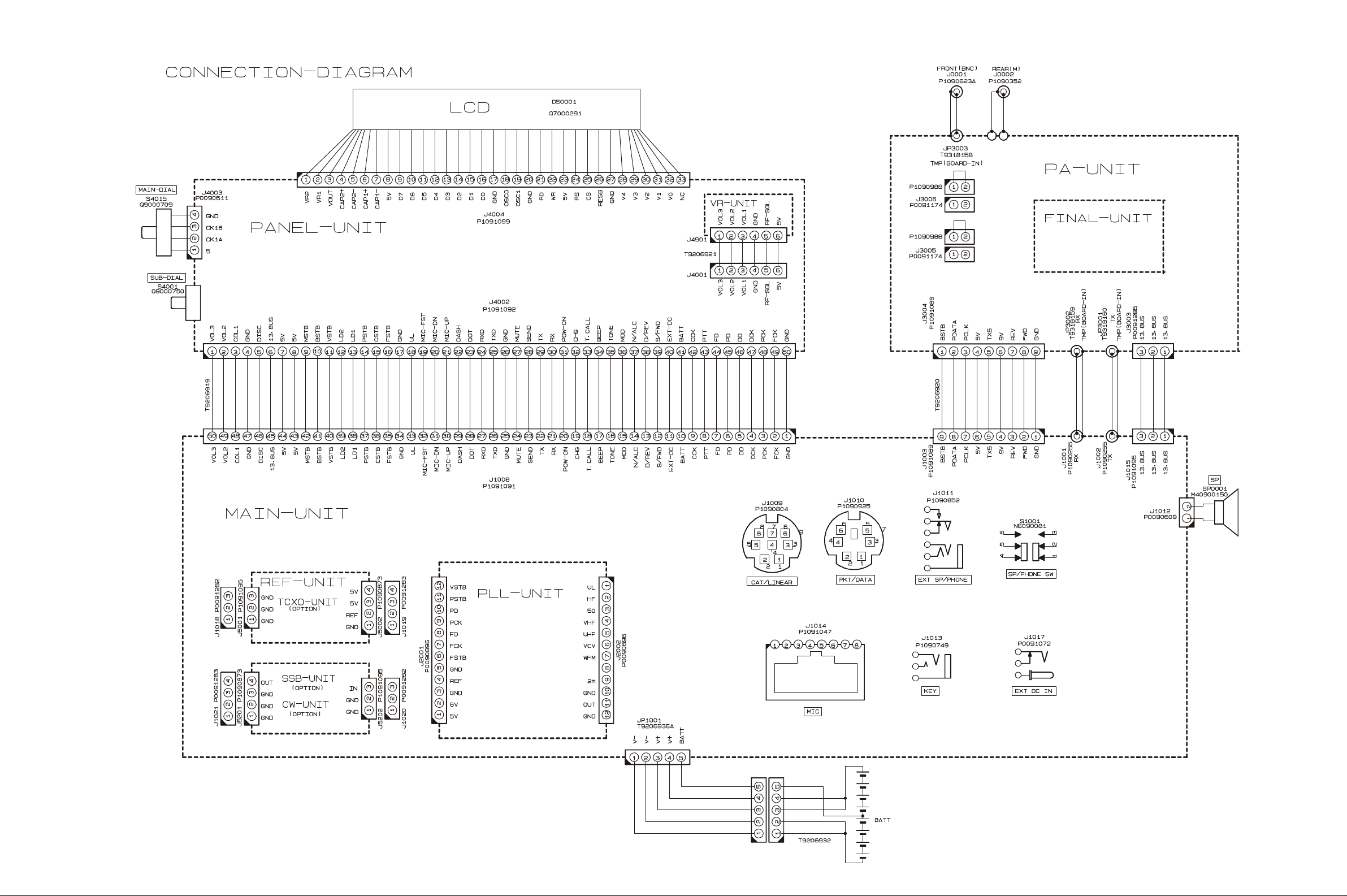
Interconnection Diagram
23

Interconnection Diagram
Note:
24
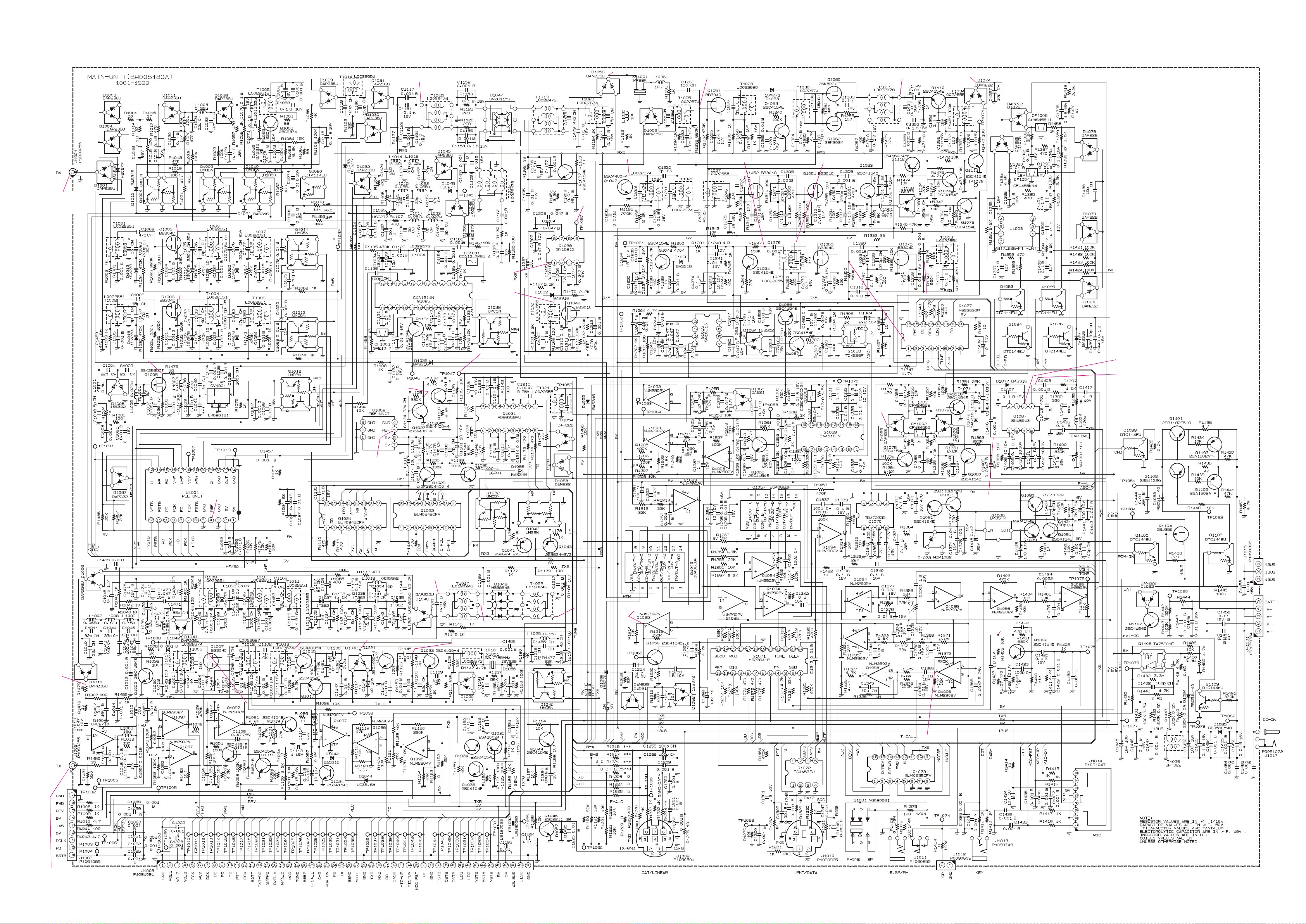
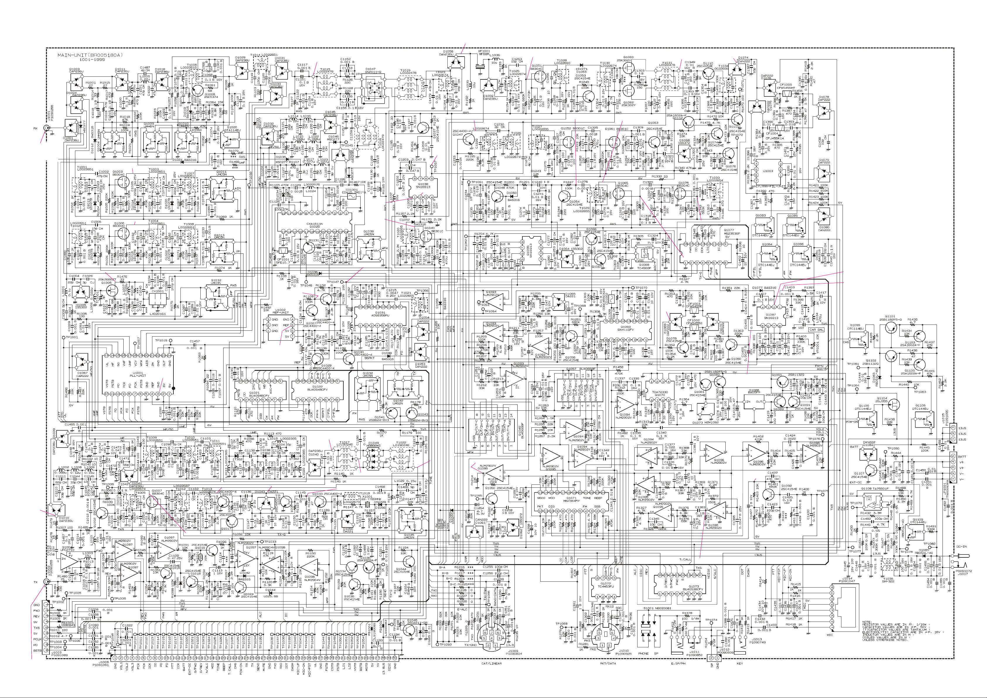
MAIN Unit
439.95 MHz: -9.0 dBµ
145.95 MHz: -9.0 dBµ
52.00 MHz: -4.1 dBµ
14.00 MHz: -5.2 dBµ
128 MHz: +13.5 dBµ
145.95 MHz:
+15.5 dBµ
145.95 MHz: +18.5 dBµ
USB mode:
(54 mVrms)
USB mode:
(350 mVrms)
200 mVrms
USB mode: (40 mVrms)
68.33 MHz: +6.1 dBµ
700 mVrms
68.33 MHz: +0.6 dBµ
455 kHz (CW mode)*: +94 dBµ
455 kHz: +36 dBµ 455 kHz: +28.5 dBµ
455 kHz (CW mode)*: +87 dBµ
455 kHz (CW mode)*: +21.5 dBµ
439.95 MHz: +21.5 dBµ
70 mVrms
90 mVrms
600 mVrms
250 mVrms
455 kHz:
+54 dBµ
455 kHz (CW mode)*: +68 dBµ
USB mode: (2.5 mVrms)
USB mode: (5.0 mVrms)
USB mode: (120 mVrms)
USB mode: (130 mVrms)
FM mode: (80 mVrms)
USB mode: (1.0 mVrms)
FM mode: (1.0 mVrms)
USB mode: (100 mVrms)
FM mode: (150 mVrms)
USB mode: (220 mVrms)
FM mode: (220 mVrms)
FM mode: (1.0 mVrms)
FM mode: (450 mVrms)FM mode: (100 mVrms)
FM mode: (150 mVrms)
FM mode: (500 mVrms)
FM mode: (11 mVrms)
USB mode:
(30 mVrms)
RX (TX)
RX: 145.95 MHz (MOD: f=1 kHz, DEV=3.5 kHz)
FM: 12 dB SINAD
*CW: S/N 10 dB
TX: 145.95 MHz, 5 W (connected to a 50-ohm dummyload)
(MIC Imput: f=1 kHz, level= 3 mVrms)
USB mode: (110 mVrms)
FM mode: (210 mVrms)
25

MAIN Unit
Note:
26
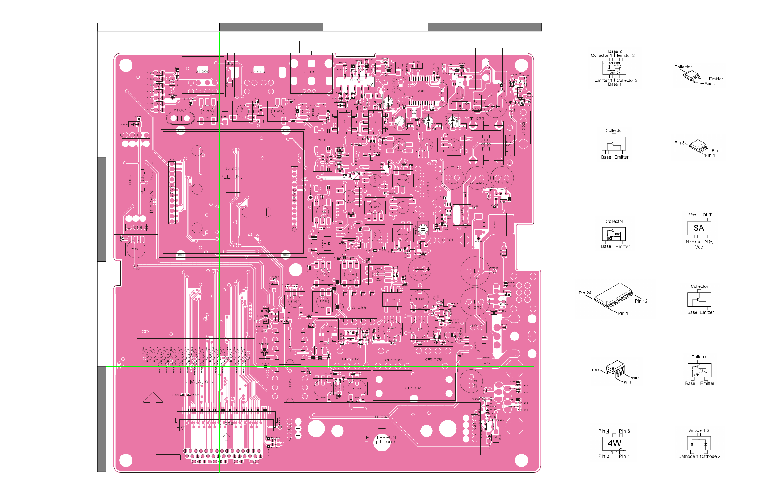
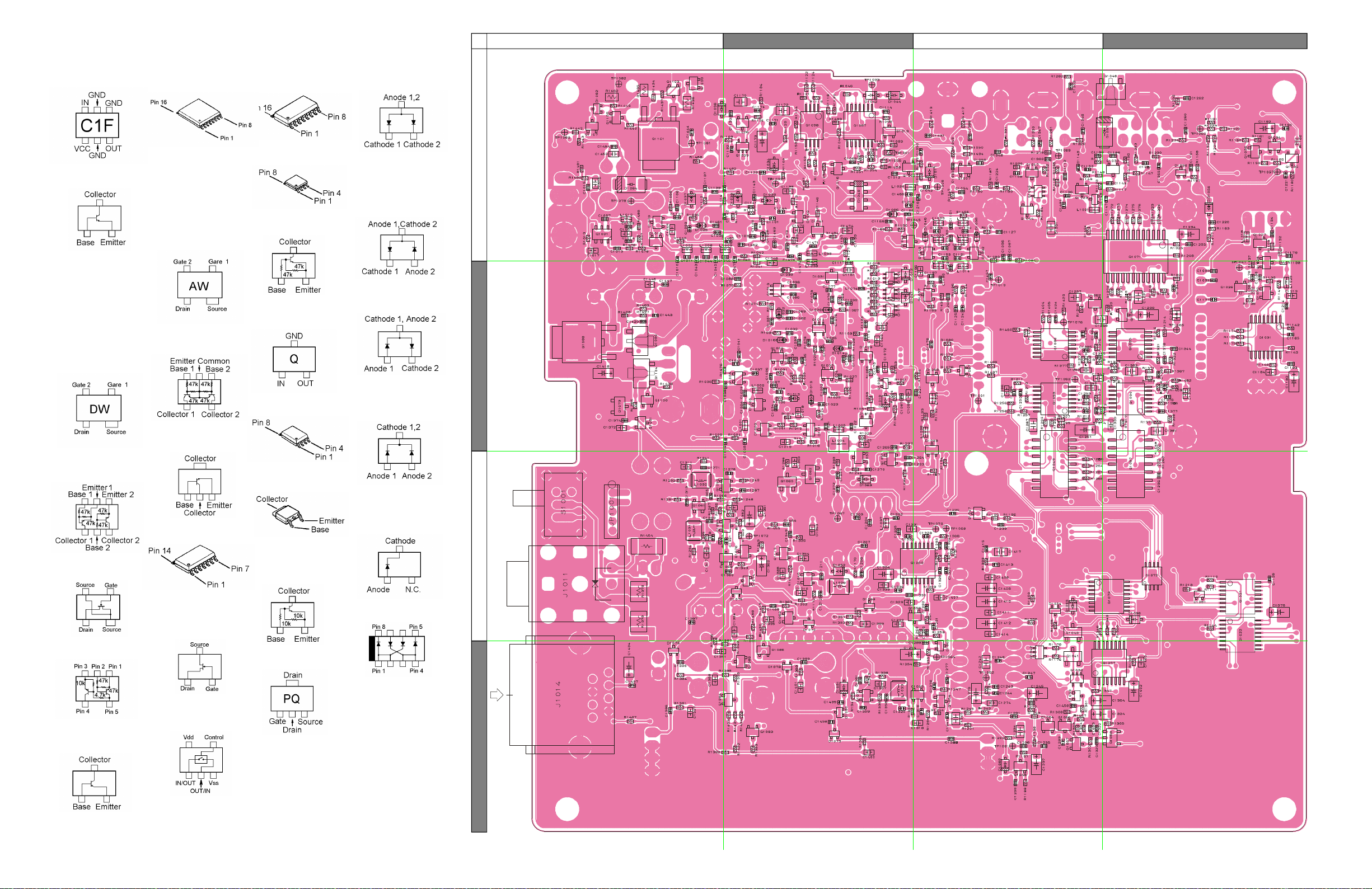
Parts Layout
A B C D
MAIN Unit
1
UMD3N (D3)
(Q1012)
2SC4154 (LE)
(Q1018, 1024, 1074, 1078,
1079, 1089, 1091, 1092, 1111)
2SC4400 (RT4)
(Q1015)
2SB1182F5
(Q1082)
2SB1132
(Q 1102)
TDA7233D
(Q1070)
2
DTA114EU (14)
(Q1020)
TA75S01F (SA)
(Q1108)
3
CXA1611N
(Q1025)
SN16913P
(Q1038, 1055, 1087)
2SA1602A (MF)
(Q1105, 1112)
DTC144EU (26)
(Q1109)
4
Side A
GN2011 (4W)
(D1047)
DAP236U (X)
(D1001, 1004, 1030)
27
MAIN Unit
a b
c d
UPC2170T (C1F)
(Q1001)
2SC4154 (LE)
(Q1002, 1016, 1017,
1019, 1026, 1034, 1036,
1037, 1044, 1048, 1050,
1053, 1054, 1056, 1063,
1066, 1067, 1076, 1080,
1081, 1107, 1110)
2SC5374 (NA)
(Q1008)
2SC4400 (RT4)
(Q1023, 1027, 1028, 1029,
1030, 1033, 1047)
2SB624 (BV3)
(Q1041, 1043)
BB304CDW (DW)
(Q1003, 1006, 1007,
1051, 1065, 1075)
UMH6N (H6)
(Q1004, 1009, 1010)
BU4094BCFV
(Q1021, 1022)
AD9835BUR
(Q1031)
BA4116FV
(Q1069)
BU4053BCFV
(Q1073)
M62353GP
(Q1077)
BB301CAW (AW)
(Q1040, 1052, 1061)
UMG2N (G2)
(Q1042)
2SD2211 (DQR)
(Q1046)
M62364FP
(Q1071)
TC4W53FU
(Q1072)
DTC144EU (26)
(Q1083, 1084, 1085,
1086, 1100, 1106)
BA05FP (Q)
(Q1088)
NJM2904V
(Q1098)
2SB1182F5
(Q1101)
2SB1132
(Q1090)
DAP236U (X)
(D1003, 1009, 1010, 1011,
1018, 1029, 1031, 1032,
1040, 1041, 1045)
DAP222 (P)
(D1054, 1069, 1070, 1075,
1076, 1078, 1079, 1087)
1SS302 (C3)
(D1005, 1064)
1SS372 (N9)
(D1062, 1068)
DA221 (K)
(D1043, 1050, 1065)
DAN222 (N)
(D1053, 1061, 1074,
1080, 1082)
DAN235U (M)
(D1048, 1058, 1059)
1
2
3
2SK2685ZT (WV-)
(Q1005)
UMC5N (C5)
(Q1011, 1013, 1032,
1039, 1045)
2SA1602A (MF)
(Q1035, 1042, 1103)
2SB624 (BV3)
(Q1041, 1043)
28
BU4066BF
(Q1049, 1057)
NJM2902V
(Q1093, 1094, 1095,
1096, 1097)
2SK302 (TY)
(Q1060, 1062)
TC4S66F (C9)
(Q1068)
DTC114EU (24)
(Q1099)
2SJ355 (PQ)
(Q1104)
HZM10B2 (29)
(D1073)
HSB88WSTR
(D1049)
4
Side B
68.33 MHz: +6.1 dBµ
MAIN Unit (Lot. 30~)
439.95 MHz: -9.0 dBµ
145.95 MHz: -9.0 dBµ
52.00 MHz: -4.1 dBµ
14.00 MHz: -5.2 dBµ
128 MHz: +13.5 dBµ
145.95 MHz:
+15.5 dBµ
145.95 MHz: +18.5 dBµ
USB mode:
(54 mVrms)
USB mode:
(350 mVrms)
200 mVrms
USB mode: (40 mVrms)
700 mVrms
68.33 MHz: +0.6 dBµ
455 kHz (CW mode)*: +94 dBµ
455 kHz: +36 dBµ 455 kHz: +28.5 dBµ
455 kHz (CW mode)*: +87 dBµ
455 kHz (CW mode)*: +21.5 dBµ
439.95 MHz: +21.5 dBµ
70 mVrms
90 mVrms
600 mVrms
250 mVrms
455 kHz:
+54 dBµ
455 kHz (CW mode)*: +68 dBµ
USB mode: (2.5 mVrms)
USB mode: (5.0 mVrms)
USB mode: (120 mVrms)
USB mode: (130 mVrms)
FM mode: (80 mVrms)
USB mode: (1.0 mVrms)
FM mode: (1.0 mVrms)
USB mode: (100 mVrms)
FM mode: (150 mVrms)
USB mode: (220 mVrms)
FM mode: (220 mVrms)
FM mode: (1.0 mVrms)
FM mode: (450 mVrms)FM mode: (100 mVrms)
FM mode: (150 mVrms)
FM mode: (500 mVrms)
FM mode: (11 mVrms)
USB mode:
(30 mVrms)
USB mode: (110 mVrms)
FM mode: (210 mVrms)
RX (TX)
RX: 145.95 MHz (MOD: f=1 kHz, DEV=3.5 kHz)
FM: 12 dB SINAD
*CW: S/N 10 dB
TX: 145.95 MHz, 5 W (connected to a 50-ohm dummyload)
(MIC Imput: f=1 kHz, level= 3 mVrms)
29

MAIN Unit (Lot. 30~)
Note:
30
 Loading...