

Page 1

HF/50 MHz TRANSCEIVER
Provided by
YAESU museum
Downloaded by
RadioAmateur.EU
FT-2000
Technical Supplement
©2006 VERTEX STANDARD CO., LTD. EH025H90A
VERTEX STANDARD CO., LTD.
4-8-8 Nakameguro, Meguro-Ku, Tokyo 153-8644, Japan
VERTEX STANDARD
US Headquarters
10900 Walker Street, Cypress, CA 90630, U.S.A.
YAESU EUROPE B.V.
P.O. Box 75525, 1118 ZN Schiphol, The Netherlands
YAESU UK LTD.
Unit 12, Sun Valley Business Park, Winnall Close
Winchester, Hampshire, SO23 0LB, U.K.
VERTEX STANDARD HK LTD.
Unit 5, 20/F., Seaview Centre, 139-141 Hoi Bun Road,
Kwun Tong, Kowloon, Hong Kong
VERTEX STANDARD (AUSTRALIA) PTY., LTD.
Normanby Business Park, Unit 14/45 Normanby Road
Notting Hill 3168, Victoria, Australia
Introduction
This manual provides technical information necessary
for servicing the FT-2000 HF/50 MHz Transceiver.
Servicing this equipment requires expertise in handling
surface-mount chip components. Attempts by non-qualified persons to service this equipment may result in permanent damage not covered by the warranty, and may
be illegal in some countries.
Two PCB layout diagrams are provided for each doublesided circuit board in the Transceiver. Each side of is referred to by the type of the majority of components installed on that side (“leaded” or “chip-only”). In most
cases one side has only chip components, and the other
has either a mixture of both chip and leaded components
(trimmers, coils, electrolytic capacitors, ICs, etc.), or leaded components only.
While we believe the technical information in this manual to be correct, VERTEX STANDARD assumes no liability for damage that may occur as a result of typographical or other errors that may be present. Your cooperation in pointing out any inconsistencies in the technical
information would be appreciated.
Contents
Specifications
Exploded View & Miscellaneous Parts
Block Diagram
Connection Diagram
Alignment
Board Unit (Schematics, Layouts & Parts)
MAIN Unit
VRF Unit
BPF Unit
ANT Unit
DVS Unit
CNTL Unit
LOCAL Unit
RX-2 Unit
PA-A Unit
TUNER-MAIN Unit
TUNER-CNTL Unit
DSP Unit
VR-A Unit
VR-B Unit
SW-A Unit
MIC Unit
JACK Unit
KEY Unit
BACK-LIGHT Unit
F-CONNECT Unit
Page 2

Specifications
Provided by
YAESU museum
Downloaded by
RadioAmateur.EU
General
Rx Frequency Range: 30 kHz - 60 MHz (operating)
160 - 6 m (specified performance, Amateur bands only)
Tx Frequency Ranges: 160 - 6 m (Amateur bands only)
Frequency Stability: ±0.5 ppm (after 1 minute @+77 °F [+25 °C])
±1.0 ppm (after 1 minute @+14 °F ~ +122 °F [–10 °C ~ +50 °C])
Operating Temperature Range: 14 °F ~ +122 °F (–10 °C ~ +50 °C)
Emission Modes: A1A (CW), A3E (AM), J3E (LSB, USB), F3E (FM),
F1B (RTTY), F1D (PACKET), F2D (PACKET)
Frequency Steps: 1/10 Hz (SSB,CW, & AM), 100 Hz (FM)
Antenna Impedance: 50 Ohms, unbalanced
16.7 - 150 Ohms, unbalanced (Tuner ON, 160 - 10 m Amateur bands)
25 - 100 Ohms, unbalanced (Tuner ON, 6 m Amateur band)
Power Consumption: Rx (no signal) 70 VA
(@117 VAC) Rx (signal present) 80 VA
Tx (100 W) 450 VA
Supply Voltage: AC: 90 VAC - 132 VAC or 180 VAC- 264 VAC
DC: DC 13.8 V ± 10%
Dimensions (WxHxD): 16.1” x 5.3” x 13.8” (410 x 135 x 350 mm)
Weight (approx.): 32 lbs (14.5 kg)
Transmitter
Power Output: 5 - 100 watts (2 - 25 watts AM carrier)
Modulation Types: J3E (SSB): Balanced,
A3E (AM): Low-Level (Early Stage),
F3E (FM): Variable Reactance
Maximum FM Deviation: ±5.0 kHz/±2.5 kHz
Harmonic Radiation: Better than –60 dB (160 - 10m Amateur bands)
Better than –70 dB (6m Amateur band)
SSB Carrier Suppression: At least 60 dB below peak output
Undesired Sideband Suppression: At least 60 dB below peak output
Audio Response (SSB): Not more than –6 dB from 300 to 2700 Hz
3rd-order IMD: –31 dB @14 MHz 100 watts PEP
Microphone Impedance: 600 Ohms (200 to 10 kOhms)
SPECIFICATIONS-1
Page 3

Specifications
Provided by
YAESU museum
Downloaded by
RadioAmateur.EU
Receiver
Circuit Type: Main (VFO-A); Triple-conversion superheterodyne
Sub (VFO-B); Double-conversion superheterodyne
Intermediate Frequencies: Main (VFO-A); 69.450 MHz/450 kHz/30 kHz (24 kHz for AM/FM),
Sub (VFO-B); 40.455 MHz/455 kHz
Sensitivity (RF AMP 2 “ON”): SSB (2.4 kHz, 10 dB S+N/N)
6 μV (0.1 - 1.8 MHz)
0.2 μV (1.8 - 30 MHz)
0.125 μV (50 - 54 MHz)
AM (6 kHz, 10 dB S+N/N, 30 % modulation @400 Hz)
3.2 μV (0.1 - 1.8 MHz)
2 μV (1.8 - 30 MHz)
1 μV (50 - 54 MHz)
FM (BW: 15 kHz, 12 dB SINAD)
0.5 μV (28 - 30 MHz)
0.35 μV (50 - 54 MHz)
There is no specification in frequency ranges not listed.
Squelch Sensitivity: SSB/CW/AM
(RF AMP 2 “ON”) 2 μV (0.1 - 30 MHz)
2 μV (50 - 54 MHz)
FM
1 μV (28 - 30 MHz)
1 μV (50 - 54 MHz)
There is no specification in frequency ranges not listed.
Selectivity (–6/–60 dB): Main (VFO-A)
Mode –6 dB –60 dB
CW/RTTY/PKT 0.5 kHz or better 750 Hz or less
SSB 2.4 kHz or better 3.6 kHz or less
AM 6 kHz or better 15 kHz or less
FM 15 kHz or better 25 kHz or less
(WIDTH: Center, VRF: OFF)
Sub (VFO-B)
Mode –6 dB –60 dB
CW/RTTY/PKT 1.1 kHz or better 3.0 kHz or less
SSB 2.2 kHz or better 4.5 kHz or less
AM 6 kHz or better 25 kHz or less
FM 12 kHz or better 30 kHz or less
Image Rejection: 70 dB or better (160 - 10m Amateur bands)
60 dB or better (6m Amateur band)
Maximum Audio Output: 2.5 W into 4 Ohms with 10% THD
Audio Output Impedance: 4 to 8 Ohms (4 Ohms: nominal)
Conducted Radiation: Less than 4000 μμW
Specifications are subject to change, in the interest of technical improvement, without notice or obligation, and
are guaranteed only within the amateur bands.
SPECIFICATIONS-2
Page 4

Specifications
Note
SPECIFICATIONS-3
Page 5
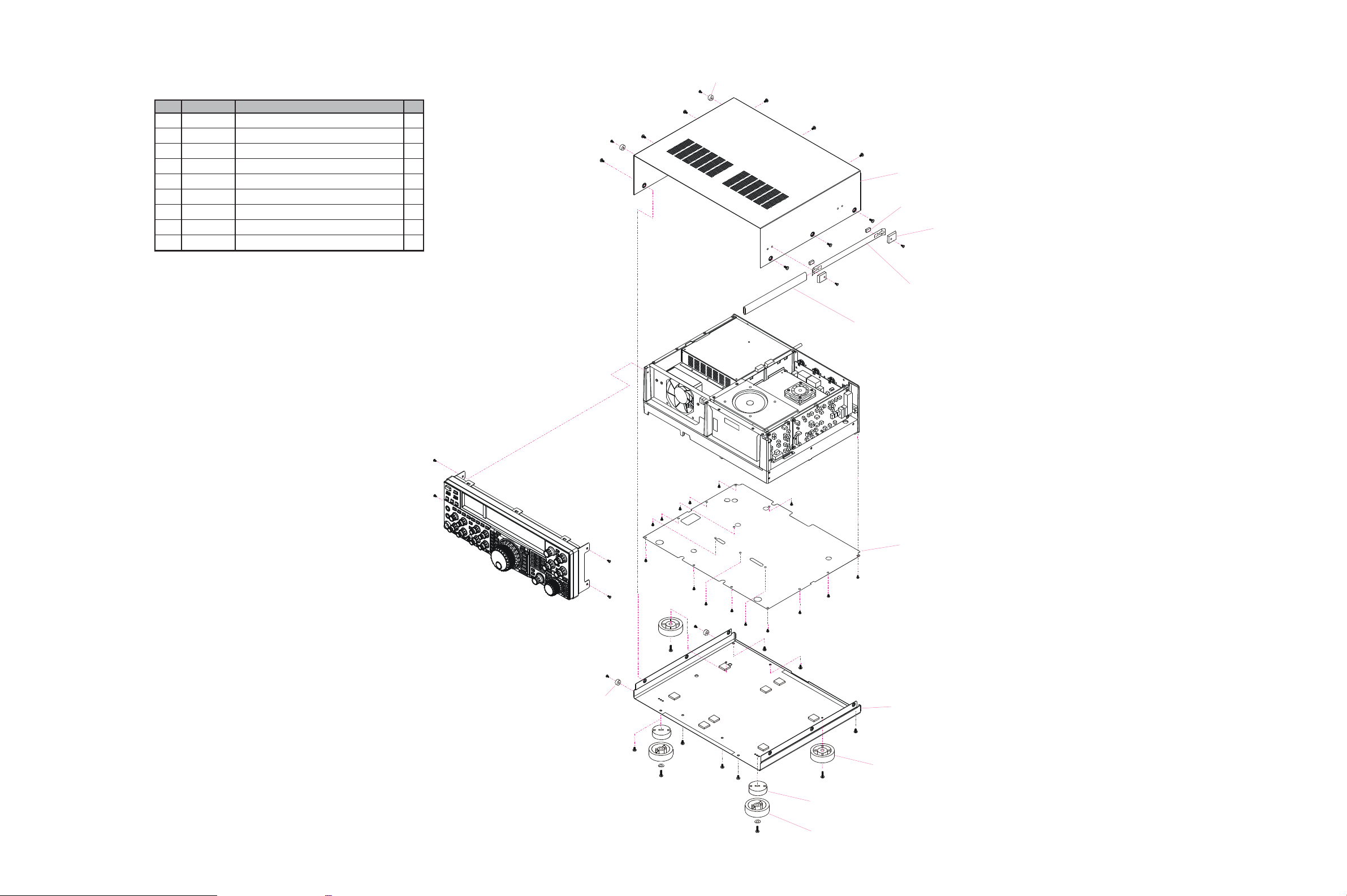
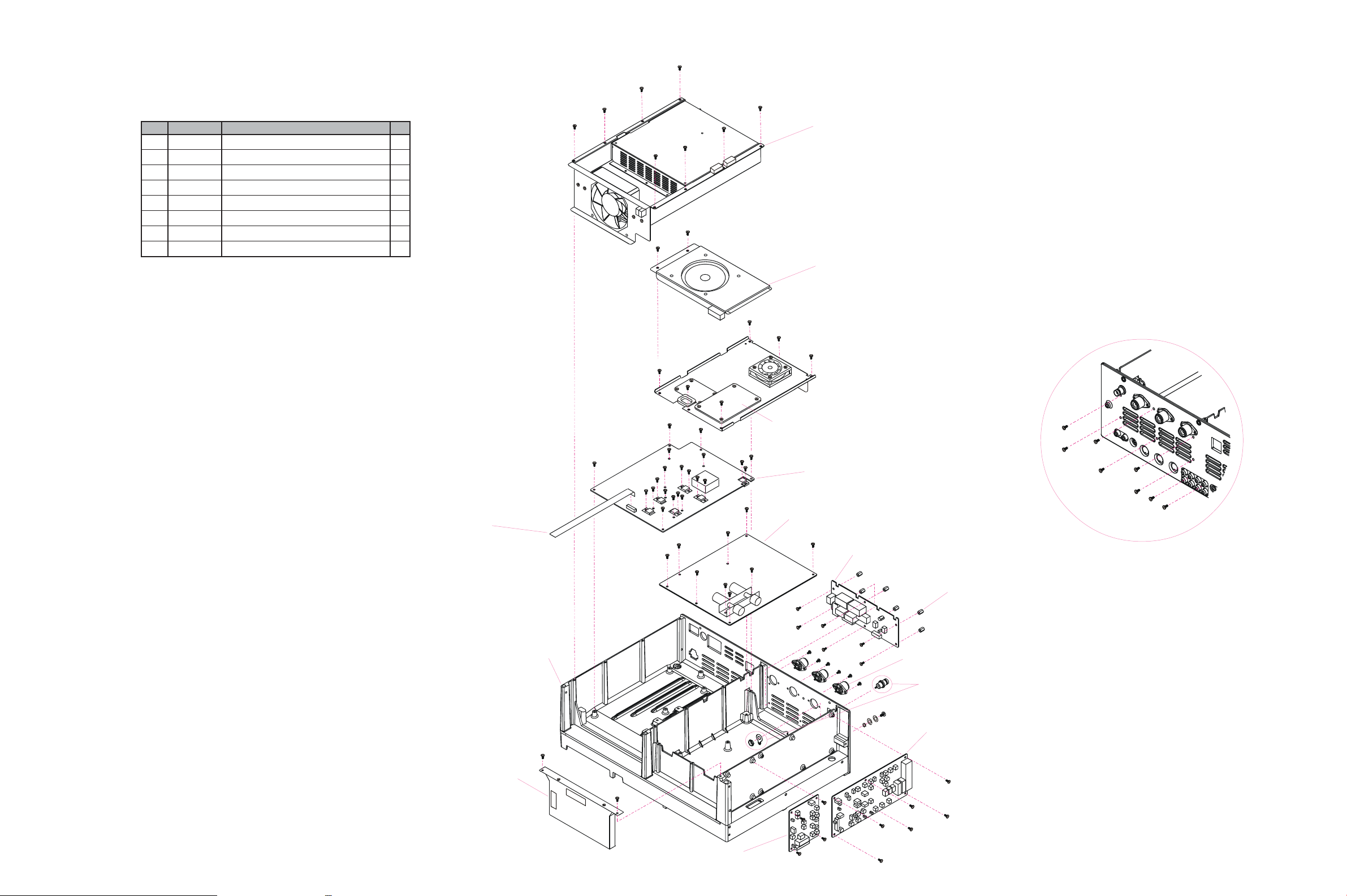
Exploded View
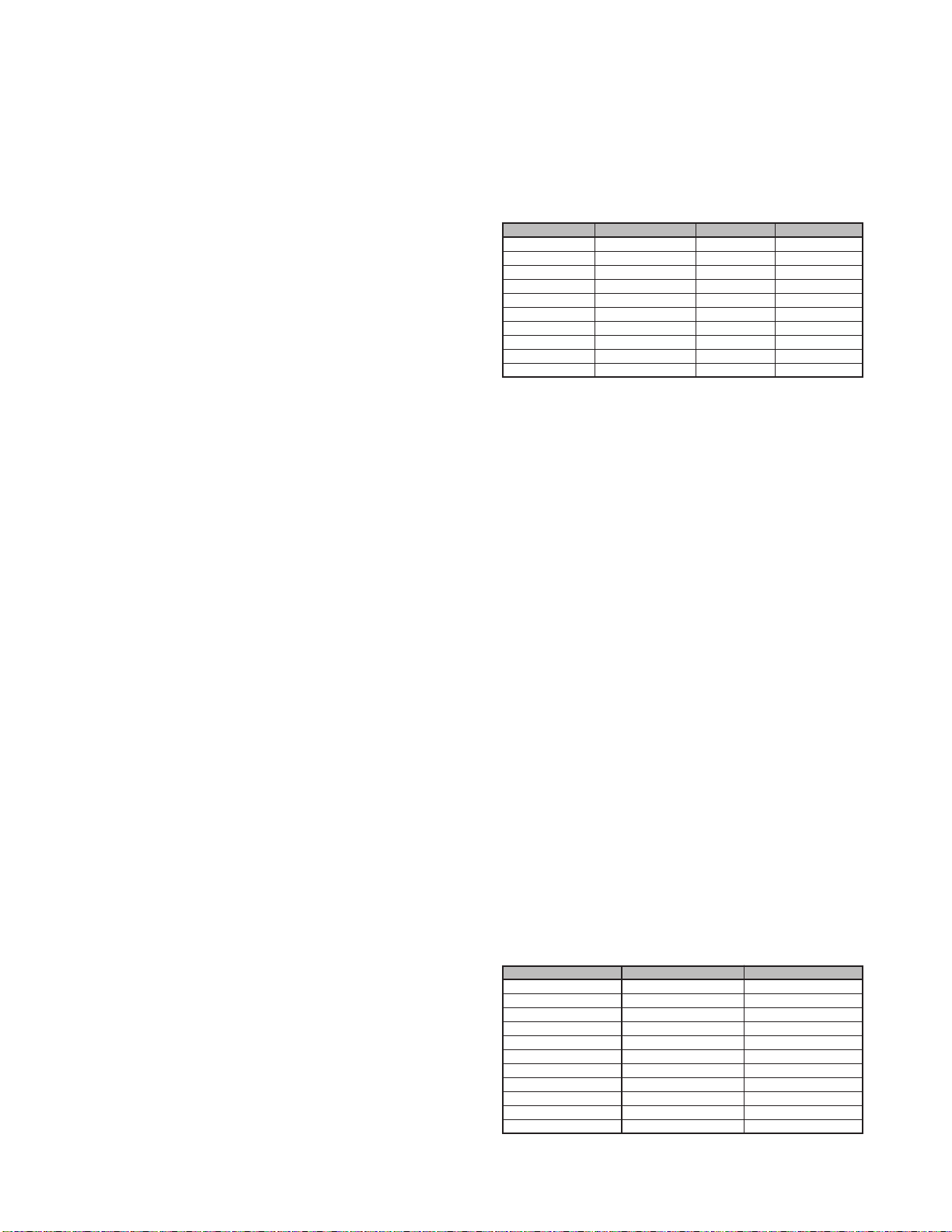
REF. VXSTD P/N Description Qty.
U31408007 OVAL HEAD SCREW M4X8B 9
U24305007 BIND HEAD TAPTITE-B M3X5B 4
U31410020 OVAL HEAD SCREW M4X10SUS 2
U31306007 OVAL HEAD SCREW M3X6B 7
U24425007 BIND HEAD TAPTITE-B M4X25B 2
U70005002 PLAIN WASHER FW5NI 2
U24410007 BIND HEAD TAPTITE-B M4X10B 2
U24306002 BIND HEAD TAPTITE-B M3X6NI 15
U34308001 FLAT HEAD TAPTITE-B M3X8 4
Non-designated parts are available only as part of a designated
assembly.
S4000047 (X2 pcs)
CASE LEG
Case ASSY
CP8644001
TOP CASE ASSY
RA0734000 (X2 pcs)
PORON SHEET
R4115020A (X2 pcs)
HANDLE END
R3084747
HANDLE (CE)
R3084746
HANDLE
R0115070A
HANDLE SHAFT
RA0831500
SHIELD CASE COVER
CS1895001
BOTTOM CASE ASSY
S4000047 (X2 pcs)
CASE LEG
RA072470A (X2 pcs)
LEG
RA072460A (X2 pcs)
LEG
RA0719500 (X2 pcs)
LEG
Exploded View-1
Page 6
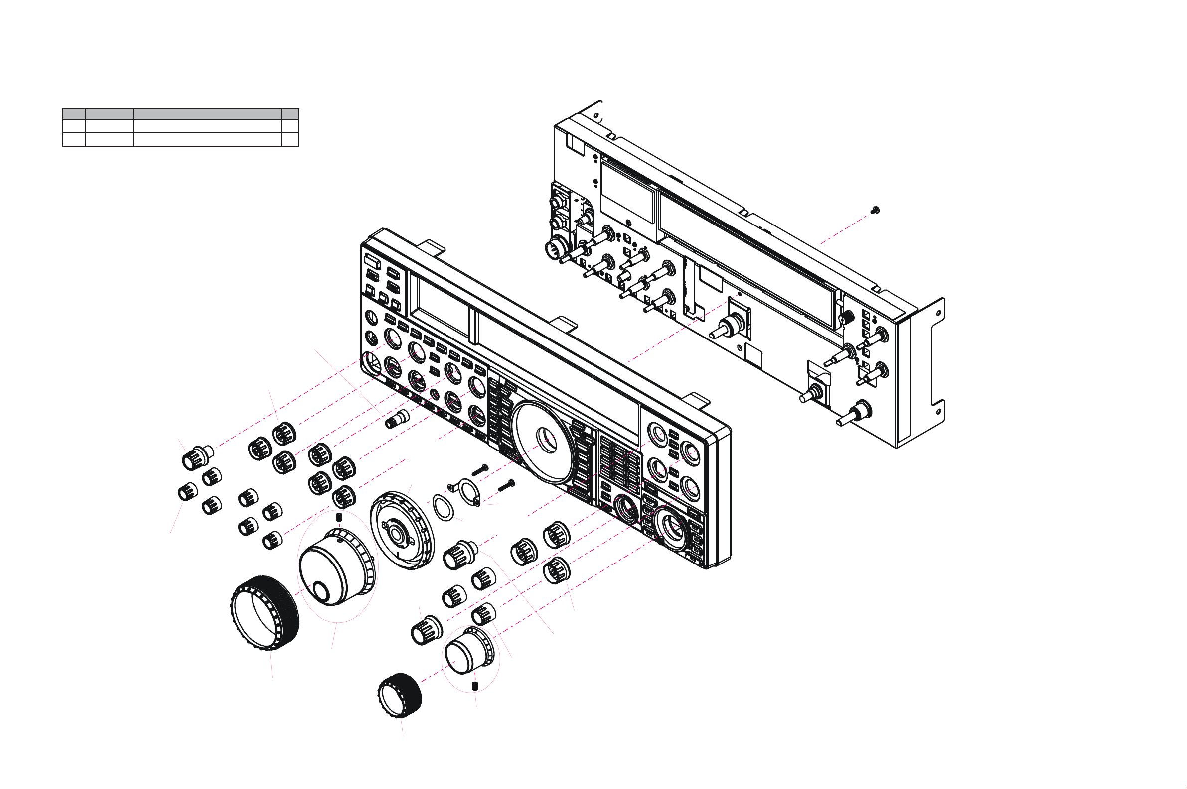
Exploded View
Panel ASSY (1/2)
REF. VXSTD P/N Description Qty.
U24205001 BIND HEAD TAPTITE-B M2.6X5 1
U24214001 BIND HEAD TAPTITE-B M2.6X14 2
Non-designated parts are available only as part of a designated
assembly.
RA0828000
ROTARY KNOB
RA0828100 (X7 pcs)
VOLUME KNOB
RA0828300
VOLUME KNOB
RA0828200 (X7 pcs)
VOLUME KNOB
RA0829000
RUBBER RING
RA0828700
ROTARY KNOB
RA0828800
KNOB MAIN ASSY
RA0833200
KNOB SKIRT
RA085250A
HOLDER
U9900211
WAVE WASHER
RA0828400 (X3 pcs)
VOLUME KNOB
RA0828500 (X3 pcs)
VOLUME KNOB
RA0828600
ROTARY KNOB
Exploded View-2
RA0829300
RUBBER RING (SUB)
RA082910A
SUB KNOB ASSY
Page 7
RA082640A
Provided by
YAESU museum
Downloaded by
RadioAmateur.EU
FRONT PANEL
R7155600 (X6 pcs)
HIMERON TAPE
RA088190A
SPONGE RUBBER
RA085260A
SPONGE RUBBER
RA0829400
WINDOW
RA084380A
KNOB ASSY
RA082670A
PUSH KNOB (NB)
SW-A Unit
RA088190A
SPONGE RUBBER
RA0826800
PUSH KNOB (BKIN)
T9207298
WIRE ASSY
RA0827600
PUSH KNOB
RA0843600
KNOB ASSY
RA0826900
PUSH KNOB (FUNC)
RA0827700
PUSH KNOB
RA082700A
PUSH KNOB
RA0832100
PUSH KNOB
RA0827400
PUSH KNOB
RA0843700
KNOB ASSY
RA085700A
SPONGE RUBBER
RA0827100
PUSH KNOB
RA085690A
SPONGE RUBBER
RA0827800
PUSH KNOB
RA0827500
PUSH KNOB
Exploded View
Panel ASSY (2/2)
T9207337
WIRE ASSY
T9207337
WIRE ASSY
T9207298
WIRE ASSY
KEY Unit
RA0836300
LIGHT GUIDE
RA082790A
PUSH KNOB
RA088200A
SPONGE RUBBER
REF. VXSTD P/N Description Qty.
U24106001 BIND HEAD TAPTITE-BM2X6 38
Non-designated parts are available only as part of a designated
assembly.
Exploded View-3
Page 8
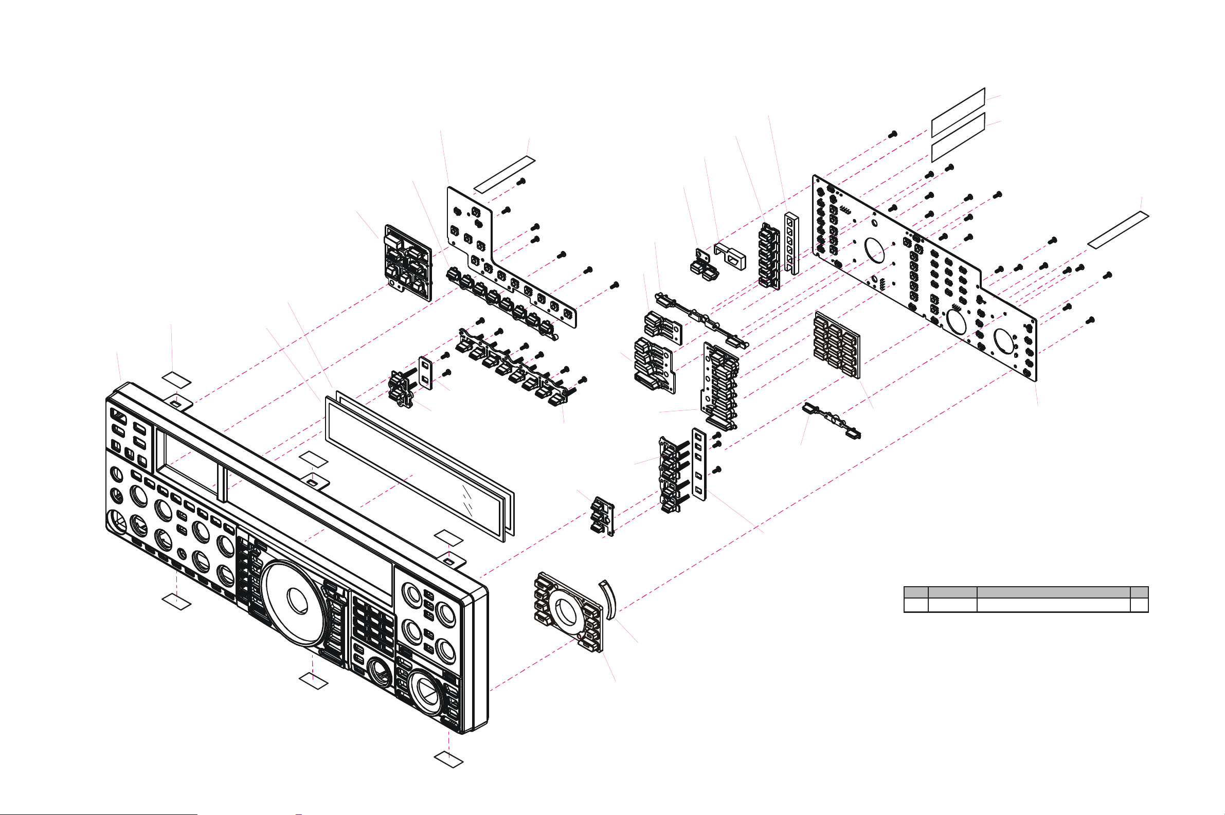
Exploded View
Panel Frame ASSY
REF. VXSTD P/N Description Qty.
U24205001 BIND HEAD TAPTITE-B M2.6X5 15
Non-designated parts are available only as part of a designated
assembly.
RA082960B
PANEL FRAME
This metal fittings are attached to CONNECTOR.
RA083690A
KNOB GUIDE
MIC Unit
JACK Unit
RA0829500
REFLECTOR
M0290075A
METER
BACK-LIGHT Unit
VR-A Unit
Q9000833
ROTARY ENCODER
RA0837100
KNOB GUIDE
(BKIN)
Q7000570
VFD MODULE
This washer are attached to SWITCH.
This nut are attached to SWITCH.
This washer are attached to CONNECTOR.
This nut are attached to CONNECTOR.
This washer are attached to VR.
This nut are attached to VR.
This washer are attached to VR.
This nut are attached to VR.
This nut are attached to VR.
This washer are attached to VR.
RA0744600
SLEEVE
RA0729400
WASHER
U9900192
WAVE WASHER
This nut are attached to ROTARY ENCODER.
This nut are attached to VR.
This washer are attached to VR.
This washer are attached to ROTARY ENCODER.
Q9000709A
ROTARY ENCODER
RA0837000
KNOB GUIDE (VRF)
VR-B Unit
Q9000833
ROTARY ENCODER
Exploded View-4
R0134990A
COIL SPRING
Page 9
Exploded View
REF. VXSTD P/N Description Qty.
U24306002 BIND HEAD TAPTITE-B M3X6NI 42
U34308001 FLAT HEAD TAPTITE-B M3X8 4
U03308002 SEMS SCREW ASM3X8NI 20
U44308002 PAN HEAD TAPTITE-B M3X8NI 8
U03306002 SEMS SCREW ASM3X6NI 4
U52415002 HEX HEAD BOLT M4X15NI 1
U70005002 PLAIN WASHER FW5NI 2
U72005002 TOOTHED LOCK WASHER OW5NI 1
Non-designated parts are available only as part of a designated
assembly.
CHASSIS ASSY (1/4)
PS ASSY
SP ASSY
T9207339
WIRE ASSY
RA082970A
CHASSIS
TUNER-CNTL Unit
TUNER-MAIN Unit
PA-A Unit
ANT Unit
S5000274 (X6 pcs)
SPACER
P1090984 (X3 pcs)
CONNECTOR
P1091246
CONNECTOR
RX-2 Unit
DSP ASSY
SCP Unit (Option)
Exploded View-5
Page 10
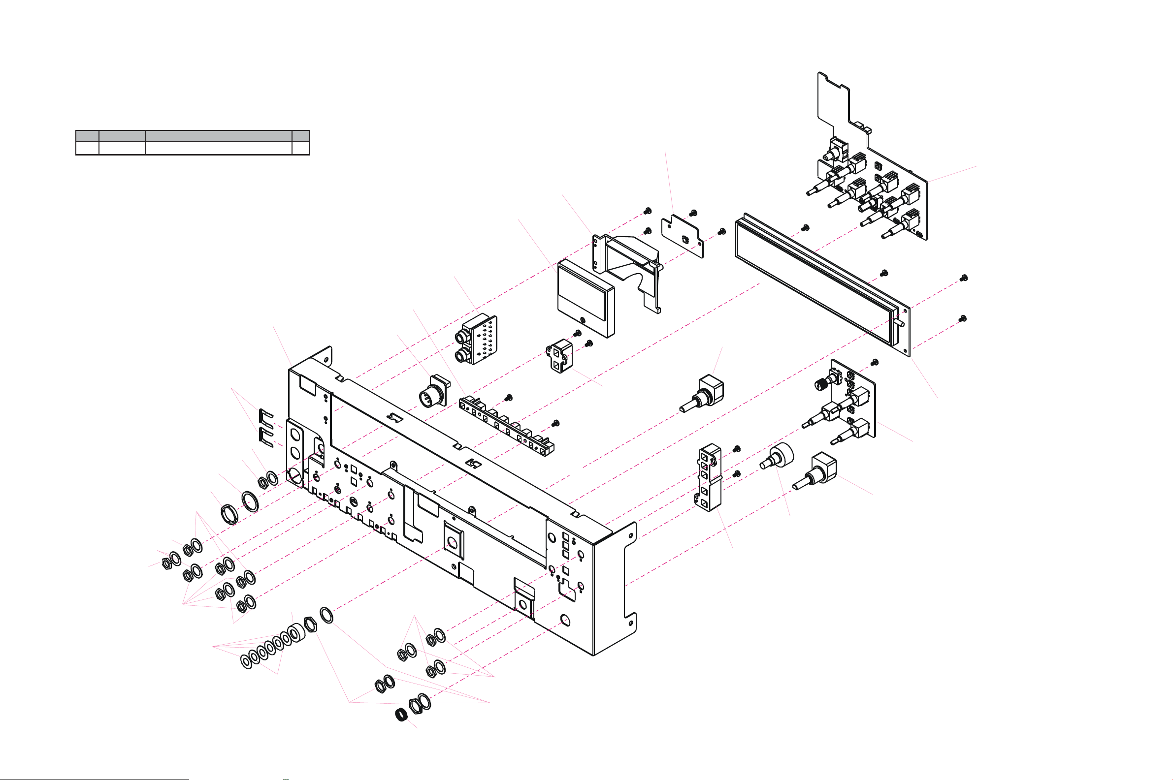
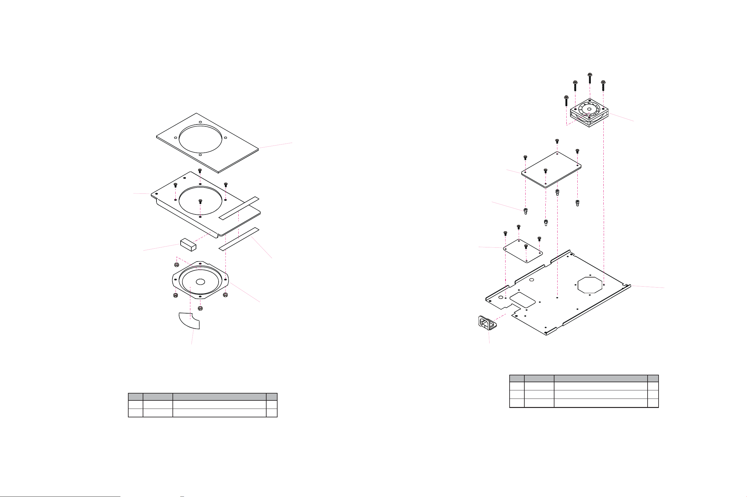
Exploded View
CHASSIS ASSY (2/4)
PS ASSY DSP ASSY
REF. VXSTD P/N Description Qty.
U24306002 BIND HEAD TAPTITE-B M3X6NI 12
U04330007 SEMS SCREW HSM3X30B 4
Non-designated parts are available only as part of a designated
assembly.
RA0831200
SHIELD CASE
Q7000572
POWER SUPPLY
Q7000573 (CE)
POWER SUPPLY
RA0532400 (X2 pcs)
GASKET
DSP UNIT
RA0831300
SHIELD CASE COVER
R0120250 (X2 pcs)
LEAF SPRING
RA083110A
SHIELD CASE COVER
RA0878100 (CE)
SHIELD CASE COVER
REF. VXSTD P/N Description Qty.
U24206002 BIND HEAD TAPTITE-B M2.6X6NI 4
U03306002 SEMS SCREW ASM3X6NI 4
Non-designated parts are available only as part of a designated
assembly.
Exploded View-6
M2090046
FAN
F-CONNECT Unit
RA0868800
MOTOR HOLDER
Page 11
Exploded View
CHASSIS ASSY (3/4)
SP ASSY TUNER ASSY
RA0859600
SPONGE RUBBER
RA0853400
SP HOLDER
RA0794800
GASKET
S5000223 (X4 pcs)
SPACER
RA083160A
SHIELD CASE COVER
RA086350A (X2 pcs)
SPONGE RUBBER
TUNER-CNTL Unit
M2090045
FAN
RA0887100
BLIND SHEET
REF. VXSTD P/N Description Qty.
M4090125
SPEAKER
U30310002 FLAT HEAD SCREW M3X10NI 4
U66300002 FLANGE NUT N3NI 4
Non-designated parts are available only as part of a designated
assembly.
S6000280
EDGE HOLDER
REF. VXSTD P/N Description Qty.
Non-designated parts are available only as part of a designated
assembly.
U04325002 SEMS SCREW HSM3X25NI 4
U03306002 SEMS SCREW ASM3X6NI 4
U24306002 BIND HEAD TAPTITE-B M3X6NI 4
RA0831000
SHIELD CASE COVER
Exploded View-7
Page 12
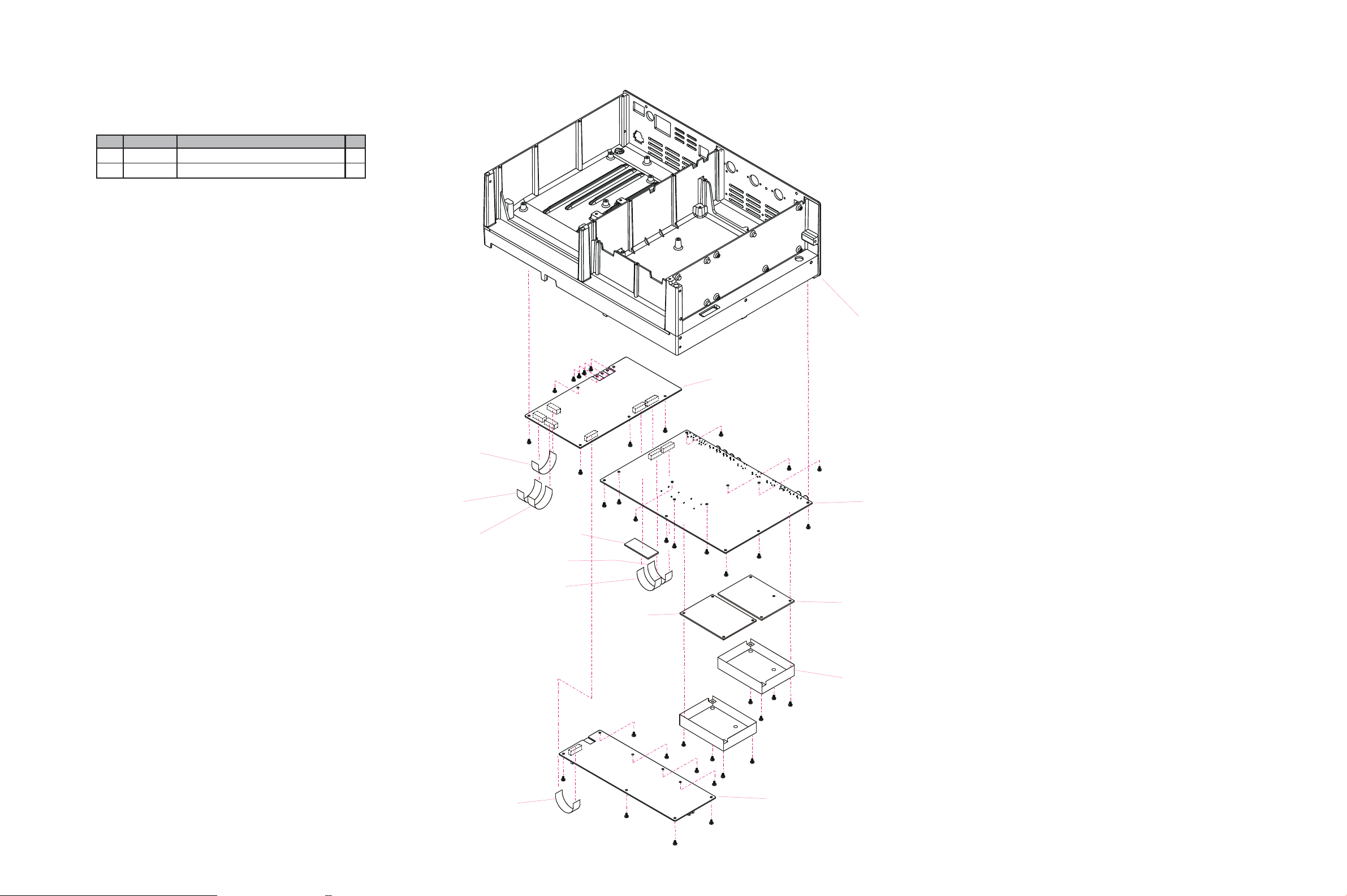
Exploded View
CHASSIS ASSY (4/4)
REF. VXSTD P/N Description Qty.
U24306002 BIND HEAD TAPTITE-B M3X6NI 2
U03306002 SEMS SCREW ASM3X6NI 4
Non-designated parts are available only as part of a designated
assembly.
RA082970A
CHASSIS
CNTL Unit
T9207115A
WIRE ASSY
T9207127A
WIRE ASSY
T9207338
WIRE ASSY
T9207337
WIRE ASSY
DVS Unit
T9207336
WIRE ASSY
T9207336
WIRE ASSY
MAIN Unit
VRF Unit
BPF Unit
RA083090A (X2 pcs)
SHIELD CASE COVER
LOCAL Unit
Exploded View-8
Page 13
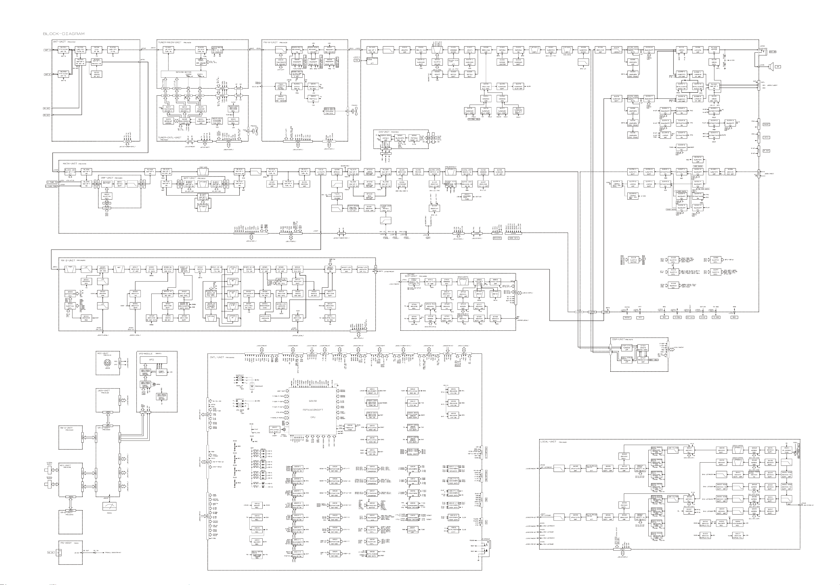
Block Diagram
Provided by
YAESU museum
Downloaded by
RadioAmateur.EU
BLOCK DIAGRAM-1
Page 14
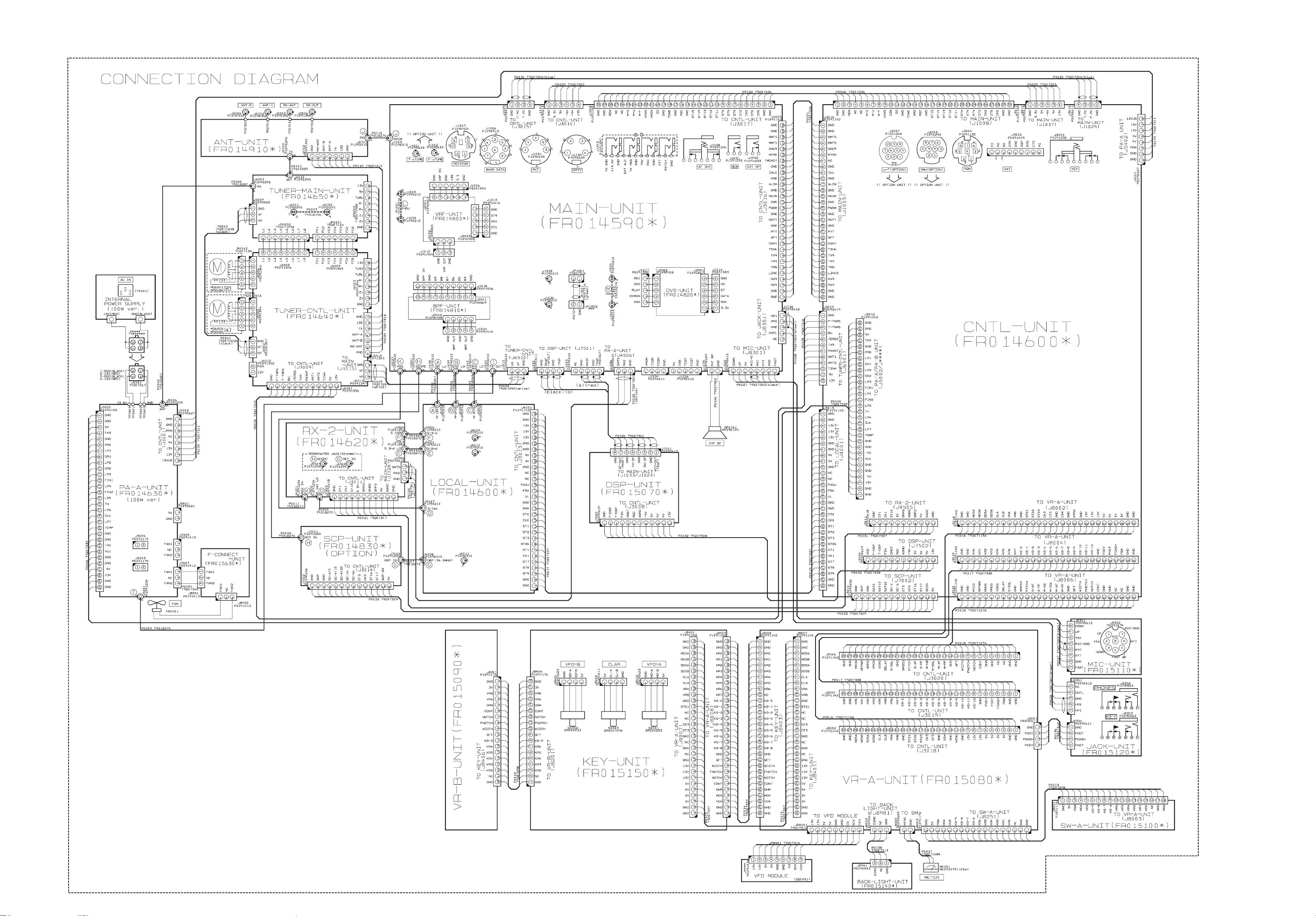
Connection Diagram
Provided by
YAESU museum
Downloaded by
RadioAmateur.EU
CONNECTION DIAGRAM-1
Page 15

Alignment
Introduction and Precautions
The following procedures cover adjustments that are
not normally required once the transceiver has left
the factory. However, If a problem occurs during
normal operation due to component failure; realignment may be required after the faulty components
have been replaced.
We recommend that authorized Vertex Standard
Technicians, who are experienced with the circuitry
and fully equipped to repair and align our products,
perform repairs. If a fault is suspected, contact the
selling dealer for instructions regarding repair. Authorized Vertex Standard Technicians have the latest information to align all circuits and make complete performance checks to ensure compliance with
factory specifications after repairs.
Those who do undertake any of the following alignments are cautioned and proceed at their own risk.
Problems caused by unauthorized attempts at realignment are not covered by the warranty policy.
Vertex Standard must reserve the right to change
circuits and alignment procedures in the interest of
improved performance, without notifying owners.
Under no circumstances should any alignment be
attempted unless the normal functions and operation of the transceiver are clearly understood, the
cause of the malfunction has been clearly identified
and all faulty components replaced. The need for
realignment should be determined to be absolutely
necessary.
The following test equipment (and a thorough familiarity with its correct use) is necessary for correct
realignment. Most steps do not require all of the
equipment listed. The interactions of some adjustments may require that more complex adjustments
be performed in a sequence. Do not attempt to perform only a single step unless it is clearly isolated
electrically from all other steps. Have all test equipment ready before beginning, and follow all of the
steps in a section in the order they are presented.
Required Test Equipment
RF Signal Generator
AF Signal Generator
Spectrum Analyzer good to at least 1 GHz.
Frequency Counter
SINAD Meter
RF Millivoltmeter
Digital DC Voltmeter (high-Z, 1 M-Ohm/V)
DC Voltmeter
DC Ammeter (20 A)
Ohmmeter
DMU-2000 Data Management Unit
50-Ohm Dummy Load (100 watts)
100-Ohm Dummy Load (100 watts)
150-Ohm Dummy Load (100 watts)
In-Line Wattmeter (100 watts, 50-Ohm)
Linear Detector
RF Coupler
4-Ohm AF Dummy Load (3 watts)
Alignment Preparation & Precautions
A 50-ohm RF Dummy load and in-line wattmeter
must be connected to the “ANT 1” jack in all procedures that call for transmission, except where specified otherwise. Correct alignment is not possible with
an antenna.
After completing one step, read the following step
to determine whether the same test equipment will
be required. If not, remove the unneeded test equipment before proceeding. (except the dummy load
and wattmeter).
Correct alignment requires that the ambient temperature be maintained constant between 68 °F ~ 86 °F
(20 °C ~ 30 °C). When the transceiver is brought into
the shop from a hot or cold enviroment, it should be
allowed time to come to room temperature before
alignment. Also, the test equipment must be thoroughly warmed up before beginning.
Whenever possible, alignments should be made with
oscillator shields and circuit boards firmly affixed in
place. Also, the test equipment must be thoroughly
warmed up before beginning.
Note: Signal levels in dB referred to in this proce-
dure are based on 0 dBμ = 0.5 μV (closed circuit).
ALIGNMENT-1
Page 16

Alignment
Analog Meter Adjustment
Press and hold in the [1(1.8)], [2(3.5)], and [3(7)]
keys, while turning the radio on, to enter the
alignment mode.
Rotate the Main Tuning Dial knob to select the
alignment parameter “A01 FSC.”
Rotate the [SUB(VFO-B)] knob so that the Main
S-meter deflects to full scale.
Press and hold in the [MENU] button for 2 sec-
onds to save the new setting and exit from the
alignment mode.
SHIFT/WIDTH Knob
Zero (Center) Adjustment
Set the SHIFT/WIDTH knobs to the 12-o’clock
position.
Set the operating mode to “USB.”
Press and hold in the [1(1.8)], [2(3.5)], and [3(7)]
keys, while turning the radio on, to enter the
alignment mode.
Rotate the Main Tuning Dial knob to select the
alignment parameter “A02 SFt.”
Rotate the [SUB(VFO-B)] knob so that the IF
SHIFT frequency is set to “±0.00” on the external
display. The center point (±0.00) is broad (17
points). Therefore, set the [SUB(VFO-B)] knob to
the center of this broad range.
Rotate the Main Tuning Dial knob to select the
alignment parameter “A03 udt.”
Rotate the [SUB(VFO-B)] knob so that the IF
bandwidth is set to “2.4 kHz” on the external display. The IF bandwidth (2.4 kHz) is broad (24
points). Therefore, set the [SUB(VFO-B)] knob to
the center of this broad range.
Press and hold in the [MENU] button for 2 sec-
onds to save the new setting and exit from the
alignment mode.
VDD Meter Adjustment
Connect the DC voltmeter to pin 6 of J5402 on
the PA-A Unit.
Switch the external display to “SWR Monitor”
page.
Press and hold in the [1(1.8)], [2(3.5)], and [3(7)]
keys, while turning the radio on, to enter the
alignment mode.
Rotate the Main Tuning Dial knob to select the
alignment parameter “A04 vdd.”
Press the [ENT] key, then rotate the [SUB(VFO-
B)] knob so that the VDD meter (Main S-meter)
reading is the same as that on the DC voltmeter.
Rotate the [VRF] knob so that the VDD meter (on
the external display) reading is same as that on
the DC voltmeter.
Press and hold in the [MENU] button for 2 sec-
onds to save the new setting and exit from the
alignment mode.
ALIGNMENT-2
Page 17
Alignment
2nd Local Oscillator (Main) Adjustment
Disconnect the coaxial cable from J4004 on the
LOCAL Unit, then connect the Frequency counter
to J4004.
Press and hold in the [1(1.8)], [2(3.5)], and [3(7)]
keys, while turning the radio on, to enter the
alignment mode.
Rotate the Main Tuning Dial knob to select the
alignment parameter “A15 FrE.”
Rotate the [SUB(VFO-B)] knob so that the Fre-
quency counter reading is “69.000 MHz.”
Press and hold in the [MENU] button for 2 sec-
onds to save the new setting and exit from the
alignment mode.
Disconnect the Frequency counter from J4004,
then connect the RF millivoltmeter to J4004.
Adjust T4003 and T4004 on the LOCAL Unit for
maximum deflection on the RF millivoltmeter
(more than –5 dBm).
Disconnect the RF millivoltmeter from J4004, then
re-connect the coaxial cable to J4004.
PLL (Main) Adjustment
Connect the Digital DC voltmeter (high-Z) to
TP4003 on the LOCAL Unit.
Disconnect the coaxial cable from J4002 on the
LOCAL Unit, then connect the RF millivoltmeter
to J4002.
Referring to the table below, adjust the listed com-
ponents for the required voltage, or confirm that
the correct voltage is present on each frequency
listed.
VFO-A FREQUENCY
11.495 MHz
0.03 MHz
25.495 MHz
11.500 MHz
41.495 MHz
25.500 MHz
60.000 MHz
41.500 MHz
ADJUST / CONFIRM
Adjust TC4001
Confirm
Adjust TC4002
Confirm
Adjust TC4003
Confirm
Adjust TC4004
Confirm
DC VOLTMETER
5.0 V ±0.1 V
At least 0.8 V
5.0 V ±0.1 V
At least 0.8 V
5.0 V ±0.1 V
At least 0.8 V
5.0 V ±0.1 V
At least 0.8 V
RF MILLIVOLTMETER
At least +3 dBm
At least +3 dBm
At least +3 dBm
At least +3 dBm
At least +3 dBm
At least +3 dBm
At least +3 dBm
At least +3 dBm
Disconnect the RF millivoltmeter from J4002, then
re-connect the coaxial cable to J4002.
PLL (Sub) Adjustment
Connect the Digital DC voltmeter (high-Z) to
TP4004 on the LOCAL Unit.
Disconnect the coaxial cable from J4007 on the
LOCAL Unit, then connect the RF millivoltmeter
to J4007.
Referring to the table below, adjust the listed com-
ponents for the required voltage, or confirm that
the correct voltage is present on each frequency
listed.
VFO-B FREQUENCY
11.495 MHz
0.03 MHz
25.495 MHz
11.500 MHz
41.495 MHz
25.500 MHz
60.000 MHz
41.500 MHz
Disconnect the RF millivoltmeter from J4007, then
re-connect the coaxial cable to J4007.
ADJUST / CONFIRM
Adjust TC4005
Confirm
Adjust TC4006
Confirm
Adjust TC4007
Confirm
Adjust TC4008
Confirm
DC VOLTMETER
5.0 V ±0.1 V
At least 0.8 V
5.0 V ±0.1 V
At least 0.8 V
5.0 V ±0.1 V
At least 0.8 V
5.0 V ±0.1 V
At least 0.8 V
RF MILLIVOLTMETER
At least +3 dBm
At least +3 dBm
At least +3 dBm
At least +3 dBm
At least +3 dBm
At least +3 dBm
At least +3 dBm
At least +3 dBm
T4003 T4004
J4004
TC4002
TC4004 J4002
TC4003
TP4003
TC4005
LOCAL UNIT ALIGNMENT POINTS
TC4006
TC4007
TC4008 J4007
TP4004TC4001
ALIGNMENT-3
Page 18
Alignment
Main Receiver Adjustment
1st Local Oscillator Adjustment
Set the following controls as indicated:
[IPO] button: AMP1
[ATT] button: OFF
[VRF] button: THRU
[R.FLT] button: AUTO
[AGC] button: AUTO
[RF GAIN] knob: Fully clockwise
[MODE] button: CW
Connect the RF millivoltmeter to TP1073 on the
MAIN Unit.
Press and hold in the [1(1.8)], [2(3.5)], and [3(7)]
keys, while turning the radio on, to enter the
alignment mode.
Select the appropriate “Alignment Parameter”
using the Main Tuning Dial knob per the chart
below, and adjust the [SUB(VFO-B)] knob for the
corresponding RF millivoltmeter reading at each
frequency.
ALIGNMENT PARAMETER
A08 L18
A09 L35
A10 L7
A11 L14
A12 L21
A13 L28
A14 L50
Press and hold in the [MENU] button for 2 sec-
onds to save the new setting and exit from the
alignment mode.
2nd/3rd
Local Level Adjustment
Connect the RF millivoltmeter to TP1021 on the
MAIN Unit.
Adjust T1034 on the MAIN Unit for maximum
deflection on the RF millivoltmeter (more than
+10 dBm).
Connect the RF millivoltmeter to TP1018 on the
MAIN Unit.
Adjust T1028 on the MAIN Unit for maximum
deflection on the RF millivoltmeter (more than
+3 dBm).
VFO-A FREQUENCY
1.850 MHz
3.570 MHz
7.100 MHz
14.200 MHz
21.200 MHz
28.700 MHz
51.500 MHz
RF MILLIVOLTMETER
0.96 Vrms (+0 Vrms/–0.04 Vrms)
0.96 Vrms (+0 Vrms/–0.04 Vrms)
0.96 Vrms (+0 Vrms/–0.04 Vrms)
0.84 Vrms (+0 Vrms/–0.04 Vrms)
0.84 Vrms (+0 Vrms/–0.04 Vrms)
0.84 Vrms (+0 Vrms/–0.04 Vrms)
0.5 Vrms (±0.05 Vrms)
IF Transformer Adjustment
Set the following controls as indicated:
[ANT 1/2] button: ANT 1
[IPO] button: AMP1
[ATT] button: OFF
[R.FLT] button: 15 kHz
[AGC] button: AUTO
[RF GAIN] knob: Fully clockwise
[VRF] button: THRU
Set the Main Band (VFO-A) frequency to 14.200
MHz in the CW mode.
Connect the AF millivoltmeter and 4 Ohm
dummy load to the EXT SP jack.
Connect the RF Signal Generator to the “ANT 1”
jack, then set the output level to 0 dBμ at the
14.200 MHz.
Adjust T1031, T1036, T1035, T1038, T1032, T1023,
and T1019 on the MAIN Unit in succession several times for maximum deflection on the AF
millivoltmeter.
If the Main S-meter deflects while adjusting, reduce the RF Signal Generator output so that the
Main S-meter does not deflect.
MCF Adjustment
Set the following controls as indicated:
[ANT 1/2] button: ANT 1
[IPO] button: AMP1
[ATT] button: OFF
[AGC] button: AUTO
[RF GAIN] knob: Fully clockwise
[VRF] button: THRU
Set the Main Band (VFO-A) frequency to 14.200
MHz in the CW mode.
Connect the AC millivoltmeter, SINAD meter,
and 4 Ohm dummy load to the EXT SP jack.
Connect the RF Signal Generator to the “ANT 1”
jack, then set the output level to 0 dBμ at the
14.200 MHz.
Set the Roofing filter bandwidth to “3 kHz” by
pressing the [R.FLT] button.
Adjust TC1002 and T1040 on the MAIN Unit in
succession several times for maximum deflection
on the AC millivoltmeter.
If the Main S-meter deflects while adjusting, reduce the RF Signal Generator output so that the
Main S-meter does not deflect.
Set the Roofing filter bandwidth to “6 kHz” by
pressing the [R.FLT] button.
ALIGNMENT-4
Page 19
Alignment
Adjust TC1001 and T1030 on the MAIN Unit in
succession several times for maximum deflection
on the AC millivoltmeter.
If the Main S-meter deflects while adjusting, reduce the RF Signal Generator output so that the
Main S-meter does not deflect.
Set the Main Band (VFO-A) frequency to 50.000
MHz in the FM mode, and set the IPO to “AMP2”
by pressing the [IPO] button.
Set the Roofing filter bandwidth to “15 kHz” by
pressing the [R.FLT] button, and set the IPO to
“AMP2” by pressing the [IPO] button.
Set the RF Signal Generator output to 0 dBμ at
the 50.000 MHz.
Adjust T1031 and T1036 on the MAIN Unit in
succession several times for maximum deflection
on the SINAD meter.
If the Main S-meter deflects while adjusting, reduce the RF Signal Generator output so that the
Main S-meter does not deflect.
IF Trap Adjustment
Set the following controls as indicated:
[ANT 1/2] button: ANT 1
[IPO] button: AMP1
[ATT] button: OFF
[R.FLT] button: AUTO
[AGC] button: AUTO
[RF GAIN] knob: Fully clockwise
[VRF] button: THRU
Set the Main Band (VFO-A) frequency to 50.000
MHz in the CW mode.
Connect the AC millivoltmeter and 4 Ohm
dummy load to the EXT SP jack.
Connect the RF Signal Generator to the “ANT 1”
jack, then set the output level to 60 dBμ at the
69.450 MHz.
Adjust T1011 on the MAIN Unit for minimum
deflection on the AC millivoltmeter.
If the Main S-meter deflects while adjusting, reduce the RF Signal Generator output so that the
Main S-meter does not deflect.
TC1002
T1040
TP1008
Pin 3 of J1015
TP1021
T1028
TP1018
T1019
T1023
T1011
TP1073
TC1001
T1031
T1030
T1036
T1035
T1038
T1034
T1032
TP1020
T1025
T1022
MAIN UNIT (RECEIVER SECTION
)
LIGNMENT POINTS
A
ALIGNMENT-5
Page 20
Alignment
Noise Blanker Circuit Adjustment
Set the following controls as indicated:
[ANT 1/2] button: ANT 1
[IPO] button: AMP1
[ATT] button: OFF
[R.FLT] button: AUTO
[AGC] button: AUTO
[NB] button: ON (for short-duration pulse noise)
[NB] knob: Fully clockwise
[RF GAIN] knob: Fully clockwise
[VRF] button: THRU
Set the Main Band (VFO-A) frequency to 14.200
MHz in the CW mode.
Connect the DC voltmeter to TP1020 on the
MAIN Unit.
Connect the RF Signal Generator to the “ANT 1”
jack, then set the output level to 30 dBμ at the
14.200 MHz.
Adjust T1025 and T1022 on the MAIN Unit for
minimum deflection on the DC voltmeter.
Turn the NB to “OFF” by pressing the [NB] but-
ton.
Scope Circuit Adjustment
Set the following controls as indicated:
[ANT 1/2] button: ANT 1
[IPO] button: AMP1
[ATT] button: OFF
[R.FLT] button: AUTO
[AGC] button: AUTO
[RF GAIN] knob: Fully clockwise
[VRF] button: THRU
Set the Main Band (VFO-A) frequency to 14.200
MHz in the CW mode.
Disconnect the coaxial cable from J1041 on the
MAIN Unit, then connect the RF millivoltmeter
to J1041.
Connect the RF Signal Generator to the “ANT 1”
jack, then set the output level to 90 dBμ at the
14.200 MHz.
Adjust T1039 on the MAIN Unit for maximum
deflection on the RF millivoltmeter.
Disconnect the RF millivoltmeter from J1041, then
re-connect the coaxial cable to J1041.
RF AGC Adjustment
Set the following controls as indicated:
[ANT 1/2] button: ANT 1
[IPO] button: AMP1
[ATT] button: OFF
[R.FLT] button: 6 kHz
[AGC] button: AUTO
[PITCH] knob: 800 Hz
[RF GAIN] knob: Fully clockwise
[VRF] button: THRU
[MODE] button: CW
Connect the RF Signal Generator to the “ANT 1”
jack, and connect the Digital DC voltmeter (highZ) to TP1008 on the MAIN Unit.
Press and hold in the [1(1.8)], [2(3.5)], and [3(7)]
keys, while turning the radio on, to enter the
alignment mode.
Select the appropriate “Alignment Parameter”
using the Main Tuning Dial knob per the chart
below, then set the RF Signal Generator output
to each frequency & level, and adjust the
[SUB(VFO-B)] knob for the corresponding DC
voltmeter reading at each frequency.
ALIGNMENT PARAMETER
B01 rGc
B02 rGc
B03 rGc
B04 rGc
B05 rGc
B06 rGc
B07 rGc
B08 rGc
B09 rGc
B10 rGc
RF SIGNAL GENERATOR
1.900 MHz, 96 dBμ
3.750 MHz, 96 dBμ
7.150 MHz, 96 dBμ
10.125 MHz, 96 dBμ
14.175 MHz, 96 dBμ
18.117 MHz, 96 dBμ
21.255 MHz, 96 dBμ
24.940 MHz, 96 dBμ
28.850 MHz, 96 dBμ
52.000 MHz, 96 dBμ
VFO-A FREQUENCY
1.900 MHz
3.750 MHz
7.150 MHz
10.125 MHz
14.175 MHz
18.117 MHz
21.255 MHz
24.940 MHz
28.850 MHz
52.000 MHz
DC VOLTMETER
1.5 V (–0V/+0.05V)
1.5 V (–0V/+0.05V)
1.5 V (–0V/+0.05V)
1.5 V (–0V/+0.05V)
1.5 V (–0V/+0.05V)
1.5 V (–0V/+0.05V)
1.5 V (–0V/+0.05V)
1.5 V (–0V/+0.05V)
1.5 V (–0V/+0.05V)
1.5 V (–0V/+0.05V)
Press and hold in the [MENU] button for 2 sec-
onds to save the new setting and exit from the
alignment mode.
ALIGNMENT-6
Page 21
Alignment
IF Gain Adjustment
Set the following controls as indicated:
[ANT 1/2] button: ANT 1
[IPO] button: AMP1
[ATT] button: OFF
[R.FLT] button: 6 kHz
[AGC] button: AUTO
[PITCH] knob: 700 Hz
[RF GAIN] knob: Fully clockwise
[VRF] button: THRU
[MODE] button: CW
Connect the AC millivoltmeter and 4 Ohm
dummy load to the EXT SP jack.
Connect the RF Signal Generator to the “ANT 1”
jack, then set the output level to 36 dBμ at the
1.900 MHz.
Set the Main Band (VFO-A) frequency to 1.900
MHz in the CW mode.
Press and hold in the [1(1.8)], [2(3.5)], and [3(7)]
keys, while turning the radio on, to enter the
alignment mode.
Adjust the Main [AF GAIN] knob so that the AC
millivoltmeter reading is “0 dB.”
Select the appropriate “Alignment Parameter”
using the Main Tuning Dial knob per the chart
below, then set the RF Signal Generator output
to each frequency & level, and adjust the
[SUB(VFO-B)] knob for the corresponding AC
millivoltmeter reading at each frequency.
ALIGNMENT PARAMETER
b11 iGn
b12 iGn
b13 iGn
b14 iGn
b15 iGn
b16 iGn
b17 iGn
b18 iGn
b19 iGn
b20 iGn
RF SIGNAL GENERATOR
1.900 MHz, 96 dBμ
3.750 MHz, 96 dBμ
7.150 MHz, 96 dBμ
10.125 MHz, 96 dBμ
14.175 MHz, 96 dBμ
18.117 MHz, 96 dBμ
21.255 MHz, 96 dBμ
24.940 MHz, 96 dBμ
28.850 MHz, 96 dBμ
52.000 MHz, 96 dBμ
VFO-A FREQUENCY
1.900 MHz
3.750 MHz
7.150 MHz
10.125 MHz
14.175 MHz
18.117 MHz
21.255 MHz
24.940 MHz
28.850 MHz
52.000 MHz
AC MILLIVOLTMETER
–1.5 dB (±0.5 dB)
–1.5 dB (±0.5 dB)
–1.5 dB (±0.5 dB)
–1.5 dB (±0.5 dB)
–1.5 dB (±0.5 dB)
–1.5 dB (±0.5 dB)
–1.5 dB (±0.5 dB)
–1.5 dB (±0.5 dB)
–1.5 dB (±0.5 dB)
–1.5 dB (±0.5 dB)
Press and hold in the [MENU] button for 2 sec-
onds to save the new setting and exit from the
alignment mode.
S-meter Adjustment
Set the following controls as indicated:
[ANT 1/2] button: ANT 1
[IPO] button: AMP1
[ATT] button: OFF
[R.FLT] button: 6 kHz
[AGC] button: AUTO
[RF GAIN] knob: Fully clockwise
[VRF] button: THRU
Connect the RF Signal Generator to the “ANT 1”
jack, then set the frequency to 14.200 MHz.
Set the Main Band (VFO-A) frequency to 14.200
MHz in the CW mode.
Press and hold in the [1(1.8)], [2(3.5)], and [3(7)]
keys, while turning the radio on, to enter the
alignment mode.
Select the appropriate “Alignment Parameter”
using the Main Tuning Dial knob per the chart
below, then set the RF Signal Generator output
to each level, and adjust the [SUB(VFO-B)] knob
for the corresponding Main S-meter defection,
then press the [ENT] key to save the new setting
at each frequency.
ALIGNMENT PARAMETER
B21 S-1
B22 S-5
B23 S-7
B24 S-9
B25 S10
B26 S20
B27 S30
B28 S40
B29 S50
B30 S60
RF SIGNAL GENERATOR
12 dBμ
24 dBμ
30 dBμ
36 dBμ
46 dBμ
56 dBμ
66 dBμ
76 dBμ
86 dBμ
96 dBμ
MAIN S-METER
S-1
S-5
S-7
S-9
S-9+10dB
S-9+20dB
S-9+30dB
S-9+40dB
S-9+50dB
S-9+60dB
Press and hold in the [MENU] button for 2 sec-
onds to save the new setting and exit from the
alignment mode.
ALIGNMENT-7
Page 22

Alignment
FM Gain Adjustment
Set the following controls as indicated:
[ANT 1/2] button: ANT 1
[IPO] button: AMP1
[ATT] button: OFF
[R.FLT] button: 15 kHz
[AGC] button: AUTO
[RF GAIN] knob: Fully clockwise
[VRF] button: THRU
Set the RF Signal Generator to 12 dBμ at the
28.8500 MHz with ±3.5 kHz deviation FM modulation of a 1 kHz audio signal.
Set the Main Band (VFO-A) frequency to 28.850
MHz in the FM-W mode.
Press and hold in the [1(1.8)], [2(3.5)], and [3(7)]
keys, while turning the radio on, to enter the
alignment mode.
Rotate the Main Tuning Dial knob to select the
alignment parameter “b32 FnG.”
Rotate the [SUB(VFO-B)] knob so that the Main
S-meter reading is “S-3.”
Press and hold in the [MENU] button for 2 sec-
onds to save the new setting and exit from the
alignment mode.
Set the RF Signal Generator to 12 dBμ at the 52.000
MHz with ±3.5 kHz deviation FM modulation of
a 1 kHz audio signal.
Set the Main Band (VFO-A) frequency to 52.000
MHz in the FM-W mode.
Press and hold in the [1(1.8)], [2(3.5)], and [3(7)]
keys, while turning the radio on, to enter the
alignment mode again.
Rotate the Main Tuning Dial knob to select the
alignment parameter “b33 FnG.”
Rotate the [SUB(VFO-B)] knob so that the Main
S-meter reading is “S-3.”
Press and hold in the [MENU] button for 2 sec-
onds to save the new setting and exit from the
alignment mode.
Sub Receiver Adjustment
2nd/3rd Local Level Adjustment
Set the following controls as indicated:
[ANT 1/2] button: ANT 1
[IPO] button: AMP1
[ATT] button: OFF
[AGC] button: AUTO
[RF GAIN] knob: Fully clockwise
[SUB RX] button: ON
Connect the RF millivoltmeter to TP4501 on the
RX-2 Unit.
Adjust T4521 and T4501 on the RX-2 Unit for
maximum deflection on the RF millivoltmeter
(more than + 8 dBm).
Connect the RF millivoltmeter to TP4502 on the
RX-2 Unit.
Adjust T4504 on the RX-2 Unit for maximum
deflection on the RF millivoltmeter (more than +
6 dBm).
IF Transformer Adjustment
Set the following controls as indicated:
[ANT 1/2] button: ANT 1
[IPO] button: AMP1
[ATT] button: OFF
[AGC] button: AUTO
[RF GAIN] knob: Fully clockwise
[SUB RX] button: ON
Set the Sub Band (VFO-B) frequency to 14.200
MHz in the CW mode.
Connect the AC millivoltmeter and 4 Ohm
dummy load to the EXT SP jack.
Connect the RF Signal Generator to the “ANT 1”
jack, then set the output level to 0 dBμ at the
14.200 MHz.
DVS Unit Adjustment
Connect the Ohmmeter lead between TP2905 and
ground on the DVS Unit.
Adjust VR2901 on the DVS Unit for 40 k-Ohms
(±200 Ohms) on the Ohmmeter.
ALIGNMENT-8
VR2901
TP2905
DVS UNIT ALIGNMENT POINTS
Page 23
Alignment
Adjust T4507, T4509, T4511, T4515, T4517, T4518,
T4519, T4516, T4513 and T4510 on the RX-2 Unit
in succession several times for maximum deflection on the AF millivoltmeter.
If the Sub S-meter deflects while adjusting, reduce the RF Signal Generator output so that the
Sub S-meter does not deflect.
MCF Adjustment
Set the following controls as indicated:
[ANT 1/2] button: ANT 1
[IPO] button: AMP2
[ATT] button: OFF
[AGC] button: AUTO
[RF GAIN] knob: Fully clockwise
[SUB RX] button: ON
Set the Sub Band (VFO-B) frequency to 52.000
MHz in the FM-W mode.
Connect the SINAD mater and 4 Ohm dummy
load to the EXT SP jack.
Connect the RF Signal Generator to the “ANT 1”
jack, then set the output level to 0 dBμ at the
52.000 MHz with ±3.5 kHz deviation FM modulation of a 1 kHz audio signal.
Adjust T4507 and T4509 on the RX-2 Unit in suc-
cession several times for maximum deflection on
the SINAD meter.
If the Sub S-meter deflects while adjusting, reduce the RF Signal Generator output so that the
Sub S-meter does not deflect.
IF Trap Adjustment
Set the following controls as indicated:
[ANT 1/2] button: ANT 1
[IPO] button: AMP1
[ATT] button: OFF
[AGC] button: AUTO
[RF GAIN] knob: Fully clockwise
[SUB RX] button: ON
Set the Sub Band (VFO-B) frequency to 50.000
MHz in the CW mode.
Connect the AC millivoltmeter and 4 Ohm
dummy load to the EXT SP jack.
Connect the RF Signal Generator to the “ANT 1”
jack, then set the output level to 60 dBμ at the
40.455 MHz.
Adjust T4520 on the RX-2 Unit for minimum de-
flection on the AC millivoltmeter.
If the Sub S-meter deflects while adjusting, reduce the RF Signal Generator output so that the
Sub S-meter does not deflect.
T4521
T4501
T4504
TP4501
T4511T4509T4507T4520
T4510 T4516
T4515
T4513
RX-2 UNIT ALIGNMENT POINTS
T4517
T4518
T4519
T4508
TP4505
T4512
TP4502
ALIGNMENT-9
Page 24
Alignment
Noise Blanker Circuit Adjustment
Set the following controls as indicated:
[ANT 1/2] button: ANT 1
[IPO] button: AMP1
[ATT] button: OFF
[AGC] button: “Sub band (VFO-B)”AUTO
[NB] button: “Sub band (VFO-B)” ON
(for short-duration pulse noise)
[NB] knob: Fully clockwise
[RF GAIN] knob: Fully clockwise
[SUB RX] button: ON
Set the Sub Band (VFO-B) frequency to 14.200
MHz in the CW mode.
Connect the DC voltmeter to TP4505 on the RX-2
Unit.
Connect the RF Signal Generator to the “ANT 1”
jack, then set the output level to 30 dBμ at the
14.200 MHz.
Adjust T4508 and T4512 on the RX-2 Unit for
minimum deflection on the DC voltmeter.
Turn the Sub band´s (VFO-B) NB to “OFF” by
pressing the [B] button followed by the [NB] button.
IF Gain Adjustment
Set the following controls as indicated:
[ANT 1/2] button: ANT 1
[IPO] button: AMP1
[ATT] button: OFF
[AGC] button: “Sub band (VFO-B)”AUTO
[PITCH] knob: 700 Hz
[RF GAIN] knob: Fully clockwise
[SUB RX] button: ON
Connect the AC millivoltmeter and 4 Ohm
dummy load to the EXT SP jack.
Connect the RF Signal Generator to the “ANT 1”
jack, then set the output level to 36 dBμ at the
1.900 MHz.
Set the Sub Band (VFO-B) frequency to 1.900 MHz
in the CW mode.
Press and hold in the [1(1.8)], [2(3.5)], and [3(7)]
keys, while turning the radio on, to enter the
alignment mode.
Adjust the Sub [AF GAIN] knob so that the AC
millivoltmeter reading is “0 dB.”
Select the appropriate “Alignment Parameter”
using the Main Tuning Dial knob per the chart
below, then set the RF Signal Generator output
to each listed level, and adjust the [SUB(VFO-B)]
knob for the corresponding AC millivoltmeter
reading at each frequency.
ALIGNMENT PARAMETER
C01 iGn
C02 iGn
C03 iGn
C04 iGn
C05 iGn
C06 iGn
C07 iGn
C08 iGn
C09 iGn
C10 iGn
RF SIGNAL GENERATOR
1.900 MHz, 9 dBμ
3.750 MHz, 9 dBμ
7.150 MHz, 9 dBμ
10.125 MHz, 9 dBμ
14.175 MHz, 9 dBμ
18.117 MHz, 9 dBμ
21.255 MHz, 9 dBμ
24.940 MHz, 9 dBμ
28.850 MHz, 9 dBμ
52.000 MHz, 9 dBμ
VFO-B FREQUENCY
1.900 MHz
3.750 MHz
7.150 MHz
10.125 MHz
14.175 MHz
18.117 MHz
21.255 MHz
24.940 MHz
28.850 MHz
52.000 MHz
AC MILLIVOLTMETER
–1.5 dB (±0.5 dB)
–1.5 dB (±0.5 dB)
–1.5 dB (±0.5 dB)
–1.5 dB (±0.5 dB)
–1.5 dB (±0.5 dB)
–1.5 dB (±0.5 dB)
–1.5 dB (±0.5 dB)
–1.5 dB (±0.5 dB)
–1.5 dB (±0.5 dB)
–1.5 dB (±0.5 dB)
Press and hold in the [MENU] button for 2 sec-
onds to save the new setting and exit from the
alignment mode.
S-meter Adjustment
Set the following controls as indicated:
[ANT 1/2] button: ANT 1
[IPO] button: AMP1
[ATT] button: OFF
[AGC] button: “Sub band (VFO-B)”AUTO
[RF GAIN] knob: Fully clockwise
[SUB RX] button: ON
Connect the RF Signal Generator to the “ANT 1”
jack, then set the frequency to 14.200 MHz.
Set the Sub Band (VFO-B) frequency to 14.200
MHz in the CW mode.
Press and hold in the [1(1.8)], [2(3.5)], and [3(7)]
keys, while turning the radio on, to enter the
alignment mode.
Select the appropriate “Alignment Parameter”
using the Main Tuning Dial knob per the chart
below, then set the RF Signal Generator output
to each listed level, and adjust the [SUB(VFO-B)]
knob until the corresponding Sub S-meter indicator just lights (i.e. Adjust to the lowest value of
each "S" unit range), then press the [ENT] key to
save the new setting at each frequency.
ALIGNMENT PARAMETER
C11 S-0
C12 S-1
C13 S-5
C14 S-7
C15 S-9
C16 S10
C17 S20
C18 S30
C19 S40
C20 S50
C21 S60
RF SIGNAL GENERATOR
9 dBμ
12 dBμ
24 dBμ
30 dBμ
36 dBμ
46 dBμ
56 dBμ
66 dBμ
76 dBμ
86 dBμ
96 dBμ
SUB S-METER
One dot
S-1
S-5
S-7
S-9
S-9+10dB
S-9+20dB
S-9+30dB
S-9+40dB
S-9+50dB
S-9+60dB
ALIGNMENT-10
Page 25

Alignment
Press and hold in the [MENU] button for 2 sec-
onds to save the new setting and exit from the
alignment mode.
RX Carrier Point Adjustment
Set the following controls as indicated:
[ANT 1/2] button: ANT 1
[IPO] button: AMP1
[ATT] button: OFF
[AGC] button: “Sub band (VFO-B)”AUTO
[RF GAIN] knob: Fully clockwise
[SUB RX] button: ON
Connect the RF Signal Generator to the “ANT 1”
jack, then set the frequency to 14.200 MHz.
Connect the AC millivoltmeter, Frequency
Counter, and 4 Ohm dummy load to the EXT SP
jack.
Set the Sub Band (VFO-B) frequency to 14.200
MHz in the CW mode.
Press and hold in the [1(1.8)], [2(3.5)], and [3(7)]
keys, while turning the radio on, to enter the
alignment mode.
Rotate the Main Tuning Dial knob to select the
alignment parameter “C22 L-C.”
Set the RF Generator frequency so that the Fre-
quency counter reading is “1 kHz,” then adjust
the Sub [AF GAIN] knob so that the AC
millivoltmeter reading is “0 dB.”
Set the RF Generator frequency so that the Fre-
quency counter reading is “300 Hz.”
Rotate the [SUB(VFO-B)] knob so that the AC
millivoltmeter reading is “–6 dB (±0.2 dB).”
Set the RF Generator frequency so that the Fre-
quency counter reading is “2.6 kHz.”
Confirm that the AC millivoltmeter reading is
better than “–6 dB.”
Rotate the Main Tuning Dial knob to select the
alignment parameter “C23 U-C.”
Set the RF Generator frequency so that the Fre-
quency counter reading is “1 kHz,” then adjust
the Sub [AF GAIN] knob so that the AC
millivoltmeter reading is “0 dB.”
Set the RF Generator frequency so that the Fre-
quency counter reading is “300 Hz.”
Rotate the [SUB(VFO-B)] knob so that the AC
millivoltmeter reading is “–6 dB (±0.2 dB).”
Set the RF Generator frequency so that the Fre-
quency counter reading is “2.6 kHz.”
Confirm that the AC millivoltmeter reading is
better than “–6 dB.”
Rotate the Main Tuning Dial knob to select the
alignment parameter “C24 LnC.”
Set the RF Generator frequency so that the Fre-
quency counter reading is “1 kHz,” then adjust
the Sub [AF GAIN] knob so that the AC
millivoltmeter reading is “0 dB.”
Set the RF Generator frequency so that the Fre-
quency counter reading is “600 Hz.”
Rotate the [SUB(VFO-B)] knob so that the AF
millivoltmeter reading is “–6 dB (±0.2 dB).”
Rotate the Main Tuning Dial knob to select the
alignment parameter “C25 UnC.”
Set the RF Generator frequency so that the Fre-
quency counter reading is “1 kHz,” then adjust
the Sub [AF GAIN] knob so that the AC
millivoltmeter reading is “0 dB.”
Set the RF Generator frequency so that the Fre-
quency counter reading is “600 Hz.”
Rotate the [SUB(VFO-B)] knob so that the AC
millivoltmeter reading is “–6 dB (±0.2 dB).”
Press and hold in the [MENU] button for 2 sec-
onds to save the new setting and exit from the
alignment mode.
ALIGNMENT-11
Page 26
Alignment
Transmitter Adjustment
TX IFT Adjustment
Disconnect the coaxial cable from J1004 on the
MAIN Unit, then connect the RF millivoltmeter
to J1004.
Set the Main Band (VFO-A) frequency to 14.200
MHz in the FM mode, then rotate the [RF PWR]
knob to the fully clockwise position.
Press the PTT button, adjust T1033, T1029, T1020,
T1014, T1010, and T1007 for maximum deflection
on the RF millivoltmeter.
Release the PTT button.
Disconnect the RF millivoltmeter from J1004, then
re-connect the coaxial cable to J1004.
TX MCF Adjustment
Disconnect the coaxial cables from J1004, J1038,
and J1039 on the MAIN Unit.
Set the Main Band (VFO-A) frequency to 28.850
MHz in the USB mode, then rotate the [RF PWR]
knob to the fully clockwise position.
Connect the Tracking Generator to J1039 and con-
nect the Spectrum Analyzer to J1020.
Set up the Spectrum Analyzer as shown below:
Center Frequency: 69.450 MHz
Span: 50 kHz
Press the PTT button. Adjust T1020 on the MAIN
Unit to obtain maximum amplitude with minimum ripple.
Disconnect the Tracking Generator from J1039
and the Spectrum Analyzer from J1020.
Connect the coaxial cables back to J1004, J1038,
and J1039.
J1004
J1020
T1007
T1010
T1033
J1038
J1041
T1006
T1014
T1020
J1039
T1029
ALIGNMENT-12
MAIN UNIT (TRANSMITTER SECTION
)
LIGNMENT POINTS
A
Page 27
Alignment
TX Scope Circuit Adjustment
Disconnect the coaxial cable from J1041 on the
MAIN Unit, then connect the RF millivoltmeter
to J1041.
Disconnect the coaxial cable from J1004 on the
MAIN Unit.
Set the Main Band (VFO-A) frequency to 14.200
MHz in the CW mode, then rotate the [RF PWR]
knob to the fully clockwise position.
Press the PTT button, then adjust T1006 for maxi-
mum deflection on the RF millivoltmeter.
Release the PTT button.
Disconnect the RF millivoltmeter from J1041, then
re-connect the coaxial cable to J1041.
Re-connect the coaxial cable to J1004.
PA-A Unit Adjustment
Preparation
Disconnect the coaxial cables from J5001 and
J5006 on the PA-A Unit, then terminate J5001 and
J5006 into a 50-Ohm resistors.
Disconnect the jumper plugs from J5003 and
J5004 on the PA-A Unit, and remove the jumper
wire that is connected between TP5031 and T5032
on the PA-A Unit.
Pre-Drive Stage Idling Current Adjustment
Connect the DC ammeter to J5003 on the PA-A
Unit.
Press and hold in the [1(1.8)], [2(3.5)], and [3(7)]
keys, while turning the radio on, to enter the
alignment mode.
J5006
TP5031
TP5032
J5004
PA-A UNIT ALIGNMENT POINTS
J5003
J5001
ALIGNMENT-13
Page 28

Alignment
Rotate the Main Tuning Dial knob to select the
alignment parameter “d01 Pdb.”
Press the PTT button, then adjust the [SUB(VFO-
B)] knob so that the DC ammeter reading is “100
mA (±5 mA).”
Release the PTT button.
Drive Stage Idling Current Adjustment
Release the PTT button.
Connect the DC ammeter to J5004 on the PA-A
Unit.
Rotate the Main Tuning Dial knob to select the
alignment parameter “d02 db1.”
Press the PTT button, then adjust the [SUB(VFO-
B)] knob so that the DC ammeter reading is “500
mA (±50 mA).”
Release the PTT button.
Rotate the Main Tuning Dial knob to select the
alignment parameter “d03 db2.”
Press the PTT button, then adjust the [SUB(VFO-
B)] knob so that the DC ammeter reading is “500
mA (±50 mA).”
Release the PTT button.
Final Stage Idling Current Adjustment
Connect the DC ammeter between TP5031 and
TP5032 on the PA-A Unit.
Rotate the Main Tuning Dial knob to select the
alignment parameter “d04 Fb1.”
Press the PTT button, then adjust the [SUB(VFO-
B)] knob so that the DC ammeter reading is “1 A
(±50 mA).”
Release the PTT button.
Rotate the Main Tuning Dial knob to select the
alignment parameter “d05 Fb2.”
Press the PTT button, then adjust the [SUB(VFO-
B)] knob so that the DC ammeter reading is “1 A
(±50 mA).”
Release the PTT button.
Termination
Press and hold in the [MENU] button for 2 sec-
onds to save the new setting and exit from the
alignment mode.
Disconnect the 50-Ohm resistors from J5001 and
J5006, then connect the coaxial cables to J5001 and
J5006.
Re-connect the jumper plugs to J5003 and J5004,
and re-connect the jumper wire between TP5031
and TP5032.
ALIGNMENT-14
Page 29
Antenna Tuner Adjustment
CM Coupler Balance Adjustment
Disconnect the coaxial cable from J6010 on the
TUNER-MAIN Unit, then connect the 50-Ohm
Dummy Load to J6010.
Connect the Digital DC voltmeter (high-Z) to pin
3 of J6009 on the TUNER-MAIN Unit.
Turn off the [TUNE] switch, then set the Main
band (VFO-A) frequency to 24.900 MHz in the
FM mode.
Press the PTT switch, then rotate the [RF PWR]
knob for 50 Watts on the Wattmeter.
Adjust TC6002 on the TUNER-MAIN Unit for
minimum deflection on the DC voltmeter (less
than 0.1 V).
Release the PTT switch, then disconnect the 50-
Ohm Dummy Load from J6010 and re-connect
the coaxial cable to J6010.
Alignment
φφ
φ
φφ
, Z-Null Adjustment
Connect the 50-Ohm Dummy Load and Wattme-
ter to the “ANT 1” jack.
Turn off the [TUNE] switch, then set the Main
Band (VFO-A) frequency to 24.900 MHz in the
FM mode.
Press the PTT switch, then rotate the [RF PWR]
knob for 50 Watts on the Wattmeter.
Release the PTT switch, then disconnect the co-
axial cable from J6001 on the TUNER-MAIN Unit,
and re-connect the 50-Ohm Dummy Load to
J6001.
Connect the Digital DC voltmeter (high-Z) be-
tween TP6001 and TP6002 on the TUNER-MAIN
Unit, then turn on the [TUNE] switch.
Press the PTT switch, then adjust TC6001 on the
TUNER-MAIN Unit for 0 V (±0.08 V) on the DC
voltmeter.
Release the PTT switch, then disconnect the 50-
Ohm Dummy Load from J6001 and re-connect
the coaxial cable to J6001.
TC6001
J6010
J6001
TP6002
TP6001
Pin 3 of J6009
TC6002
TUNER-MAIN UNIT ALIGNMENT POINTS
ALIGNMENT-15
Page 30
Alignment
Transmitter Section Alignment Mode
Preparation
Referring to table below, tune the Main Band
(VFO-A) to each frequency listed.
BAND
1.8 MHz Band
3.5 MHz Band
7 MHz Band
10 MHz Band
14 MHz Band
18 MHz Band
21 MHz Band
24.5 MHz Band
28 MHz Band
50 MHz Band
VFO-A FREQUENCY
1.820 MHz
3.570 MHz
7.050 MHz
10.100 MHz
14.200 MHz
18.100 MHz
21.200 MHz
24.900 MHz
29.690 MHz
53.900 MHz
UK: 51.900 MHz, EU: 50.390 MHz, FRA: 51.190 MHz
Ú
Ú
Connect the 50-Ohm Dummy Load and Wattme-
ter to the “ANT 1” jack.
Connect the Audio Generator to
pin 8 of the MIC jack (pin 7:
GND), then set the output level
to 0.5 mV @1 kHz.
ALC Adjustment
Press and hold in the [1(1.8)], [2(3.5)], and [3(7)]
keys, while turning the radio on, to enter the
alignment mode.
Rotate the Main Tuning Dial knob to select the
alignment parameter “d08 iAL” for the 1.8 MHz
amateur band´s ALC Adjustment, then rotate the
[SUB(VFO-B)] knob so that the VFO-B frequency
display shows “0020.”
Rotate the [MIC] knob to the fully counter-clock-
wise position.
Press the PTT switch, then gently rotate the [MIC]
knob to the fully clockwise position.
Rotate the [SUB(VFO-B)] knob for 115 W (+5W/–
0W) on the Wattmeter.
Release the PTT switch.
Rotate the Main Tuning Dial knob to select the
alignment parameter “d09 iAL” for the 3.5 MHz
amateur band´s ALC Adjustment, then rotate the
[SUB(VFO-B)] knob so that the VFO-B frequency
display shows “0020.”
Rotate the [MIC] knob to the fully counter-clock-
wise position.
Press the PTT switch, then gently rotate the [MIC]
knob to the fully clockwise position.
Rotate the [SUB(VFO-B)] knob for 115 W (+5W/–
0W) on the Wattmeter.
Release the PTT switch.
Rotate the Main Tuning Dial knob to select the
alignment parameter “d10 iAL”for the 7 MHz
amateur band´s ALC Adjustment, then rotate the
MIC IN
MODE
USB
USB
USB
USB
USB
USB
USB
USB
USB
USB
MIC GND
[SUB(VFO-B)] knob so that the VFO-B frequency
display shows “0020.”
Rotate the [MIC] knob to the fully counter-clock-
wise position.
Press the PTT switch, then gently rotate the [MIC]
knob to the fully clockwise position.
Rotate the [SUB(VFO-B)] knob for 115 W (+5W/–
0W) on the Wattmeter.
Release the PTT switch.
Rotate the Main Tuning Dial knob to select the
alignment parameter “d11 iAL”for the 10 MHz
amateur band´s ALC Adjustment, then rotate the
[SUB(VFO-B)] knob so that the VFO-B frequency
display shows “0020.”
Rotate the [MIC] knob to the fully counter-clock-
wise position.
Press the PTT switch, then gently rotate the [MIC]
knob to the fully clockwise position.
Rotate the [SUB(VFO-B)] knob for 115 W (+5W/–
0W) on the Wattmeter.
Release the PTT switch.
Rotate the Main Tuning Dial knob to select the
alignment parameter “d12 iAL”for the 14 MHz
amateur band´s ALC Adjustment, then rotate the
[SUB(VFO-B)] knob so that the VFO-B frequency
display shows “0020.”
Rotate the [MIC] knob to the fully counter-clock-
wise position.
Press the PTT switch, then gently rotate the [MIC]
knob to the fully clockwise position.
Rotate the [SUB(VFO-B)] knob for 115 W (+5W/–
0W) on the Wattmeter.
Release the PTT switch.
Rotate the Main Tuning Dial knob to select the
alignment parameter “d13 iAL”for the 18 MHz
amateur band´s ALC Adjustment, then rotate the
[SUB(VFO-B)] knob so that the VFO-B frequency
display shows “0020.”
Rotate the [MIC] knob to the fully counter-clock-
wise position.
Press the PTT switch, then gently rotate the [MIC]
knob to the fully clockwise position.
Rotate the [SUB(VFO-B)] knob for 115 W (+5W/–
0W) on the Wattmeter.
Release the PTT switch.
Rotate the Main Tuning Dial knob to select the
alignment parameter “d14 iAL”for the 21 MHz
amateur band´s ALC Adjustment, then rotate the
[SUB(VFO-B)] knob so that the VFO-B frequency
display shows “0020.”
ALIGNMENT-16
Page 31

Alignment
Rotate the [MIC] knob to the fully counter-clock-
wise position.
Press the PTT switch, then gently rotate the [MIC]
knob to the fully clockwise position.
Rotate the [SUB(VFO-B)] knob for 115 W (+5W/–
0W) on the Wattmeter.
Release the PTT switch.
Rotate the Main Tuning Dial knob to select the
alignment parameter “d15 iAL”for the 24 MHz
amateur band´s ALC Adjustment, then rotate the
[SUB(VFO-B)] knob so that the VFO-B frequency
display shows “0020.”
Rotate the [MIC] knob to the fully counter-clock-
wise position.
Press the PTT switch, then gently rotate the [MIC]
knob to the fully clockwise position.
Rotate the [SUB(VFO-B)] knob for 100 W (+5W/–
0W) on the Wattmeter, then rotate the [SUB(VFOB)] knob so that the VFO-B frequency indication
“10” increase.
Release the PTT switch.
Rotate the Main Tuning Dial knob to select the
alignment parameter “d16 iAL”for the 28 MHz
amateur band´s ALC Adjustment, then rotate the
[SUB(VFO-B)] knob so that the VFO-B frequency
display shows “0020.”
Rotate the [MIC] knob to the fully counter-clock-
wise position.
Press the PTT switch, then gently rotate the [MIC]
knob to the fully clockwise position.
Rotate the [SUB(VFO-B)] knob for 100 W (+5W/–
0W) on the Wattmeter, then rotate the [SUB(VFOB)] knob so that the VFO-B frequency indication
“10” increase.
Release the PTT switch.
Rotate the Main Tuning Dial knob to select the
alignment parameter “d17 iAL”for the 50 MHz
amateur band´s ALC Adjustment, then rotate the
[SUB(VFO-B)] knob so that the VFO-B frequency
display shows “0020.”
Rotate the [MIC] knob to the fully counter-clock-
wise position.
Press the PTT switch, then gently rotate the [MIC]
knob to the fully clockwise position.
Rotate the [SUB(VFO-B)] knob for 100 W (+5W/–
0W) on the Wattmeter, then rotate the [SUB(VFOB)] knob so that the VFO-B frequency indication
“10” increase.
Release the PTT switch.
Press and hold in the [MENU] button for 2 sec-
onds to save the new setting and exit from the
alignment mode.
Power Adjustment
Connect the 50-Ohm Dummy Load and Wattme-
ter to the “ANT 1” jack.
Rotate the [RF PWR] knob to fully clockwise.
Set the Main Band (VFO-A) frequency to 14.200
MHz in the CW mode.
Press and hold in the [1(1.8)], [2(3.5)], and [3(7)]
keys, while turning the radio on, to enter the
alignment mode.
Rotate the Main Tuning Dial knob to select the
alignment parameter “d22AP2h.”
Rotate the [SUB(VFO-B)] knob so that the VFO-B
frequency display shows “0.”
Press the PTT switch, then rotate the [SUB(VFO-
B)] knob for 100 W (+5 W/–0 W) on the Wattmeter, and confirm the the Sub S-meter is deflect.
Release the PTT switch.
Press and hold in the [MENU] button for 2 sec-
onds to save the new setting and exit from the
alignment mode.
ALC Meter Adjustment
Connect the 50-Ohm Dummy Load and Wattme-
ter to the “ANT 1” jack.
Connect the Audio Generator to
pin 8 of the MIC jack (pin 7:
GND), then set the output level
to +0 mV @1 kHz.
Set the Main Band (VFO-A) frequency to 14.200
MHz in the USB mode.
Rotate the [MIC] knob to the 12 o’clock position,
and rotate the [RF PWR] knob to the fully clockwise position.
Press and hold in the [1(1.8)], [2(3.5)], and [3(7)]
keys, while turning the radio on, to enter the
alignment mode.
Rotate the Main Tuning Dial knob to select the
alignment parameter “d50 ALC.”
Press the PTT switch, then adjust the Audio Gen-
erator output level to the position where the ALC
meter just starts to deflect.
Release the PTT switch, then increase the Audio
Generator output level for “9 dB.”
Press the [ENT] key, while pressing and holding
in the PTT switch, then rotate the [SUB(VFO-B)]
knob for maximum deflection on the ALC meter
zone (S9+10dB).
MIC IN
MIC GND
ALIGNMENT-17
Page 32

Alignment
Release the PTT switch, then press and hold in
the [MENU] button for 2 seconds to save the new
setting and exit from the alignment mode.
TX Output Power/PO Meter/TXG Adjustment
Referring to table below, tune the transceiver to
each frequency listed.
BAND
1.8 MHz Band
3.5 MHz Band
7 MHz Band
10 MHz Band
14 MHz Band
18 MHz Band
21 MHz Band
24.5 MHz Band
28 MHz Band
50 MHz Band
VFO-A FREQUENCY
1.820 MHz
3.570 MHz
7.050 MHz
10.100 MHz
14.200 MHz
18.100 MHz
21.200 MHz
24.900 MHz
28.700 MHz
52.000 MHz
UK: 51.000 MHz, EU: 50.250 MHz, FRA: 50.700 MHz
Ú
Ú
MODE
CW
CW
CW
CW
CW
CW
CW
CW
CW
CW
Connect the 50-Ohm Dummy Load and Wattme-
ter to the “ANT 1” jack.
Set the Main Band (VFO-A) frequency to 1.820
MHz in the CW mode.
Press and hold in the [1(1.8)], [2(3.5)], and [3(7)]
keys, while turning the radio on, to enter the
alignment mode.
Rotate the Main Dial knob to select the alignment
parameter “d18AP2h.”
Rotate the [SUB(VFO-B)] knob so that the VFO-B
frequency display shows “0.”
Rotate the [VRF] knob for 100 W on the PO meter.
Press the PTT switch, then rotate the [SUB(VFO-
B)] knob for 100 W on the Wattmeter.
Rotate the [CLAR] knob so that the Sub S-meter
deflects to “S-9.”
Release the PTT switch.
Perform the same procedures for the Alignment
Menus “d18bP1h” through “d27EP10,” per the
chart at the right.
AM-TXG Adjustment
Connect the 50-Ohm Dummy Load and Wattme-
ter to the “ANT 1” jack.
Rotate the [RF PWR] knob to fully clockwise.
Set the Main Band (VFO-A) frequency to 14.200
MHz in the AM mode.
Press and hold in the [1(1.8)], [2(3.5)], and [3(7)]
keys, while turning the radio on, to enter the
alignment mode.
Rotate the Main Tuning Dial knob to select the
alignment parameter “d29 tCA.”
Rotate the [SUB(VFO-B)] knob so that the VFO-B
frequency display shows “0.”
ALIGNMENT-18
Press the PTT switch without microphone input,
then rotate the [SUB(VFO-B)] knob for 35 W (±5
W) on the Wattmeter.
Release the PTT switch.
Press and hold in the [MENU] button for 2 sec-
onds to save the new setting and exit from the
alignment mode.
ALIGNMENT MENU
d18bP1h
d18bP1h
d18cP50
1.9 MHZ3.5 MHZ7 MHZ10 MHZ14 MHZ18 MHZ21 MHZ24 MHZ
d18dP20
d18EP10
d19AP2h
d19bP1h
d19cP50
d19dP20
d20EP10
d20AP2h
d20bP1h
d20cP50
d20dP20
d20EP10
d21AP2h
d21bP1h
d21cP50
d21dP20
d21EP10
d22AP2h
d22bP1h
d22cP50
d22dP20
d22EP10
d23AP2h
d23bP1h
d23cP50
d23dP20
d23EP10
d24AP2h
d24bP1h
d24cP50
d24dP20
d24EP10
d25AP2h
d25bP1h
d25cP50
d25dP20
d25EP10
d26AP2h
d26bP1h
d26cP50
28 MHZ50 MHZ
d26dP20
d26EP10
d27AP2h
d27bP1h
d27cP50
d27dP20
d27EP10
VFO-B FREQ. DISPLAY
0
0
0
0
0
0
0
0
0
0
0
0
0
0
0
0
0
0
0
0
0
0
0
0
0
0
0
0
0
0
0
0
0
0
0
0
0
0
0
0
0
0
0
0
0
0
0
0
0
0
PO METER
100 W
50 W
20 W
10 W
5 W
100 W
50 W
20 W
10 W
5 W
100 W
50 W
20 W
10 W
5 W
100 W
50 W
20 W
10 W
5 W
100 W
50 W
20 W
10 W
5 W
100 W
50 W
20 W
10 W
5 W
100 W
50 W
20 W
10 W
5 W
100 W
50 W
20 W
10 W
5 W
100 W
50 W
20 W
10 W
5 W
100 W
50 W
20 W
10 W
5 W
WATTMETER
100 W
50 W
20 W
10 W
5 W
100 W
50 W
20 W
10 W
5 W
100 W
50 W
20 W
10 W
5 W
100 W
50 W
20 W
10 W
5 W
100 W
50 W
20 W
10 W
5 W
100 W
50 W
20 W
10 W
5 W
100 W
50 W
20 W
10 W
5 W
100 W
50 W
20 W
10 W
5 W
100 W
50 W
20 W
10 W
5 W
100 W
50 W
20 W
10 W
5 W
SUB S-METER
S-9
S-9
S-9
S-9
S-9
S-9
S-9
S-9
S-9
S-9
S-9
S-9
S-9
S-9
S-9
S-9
S-9
S-9
S-9
S-9
S-9
S-9
S-9
S-9
S-9
S-9
S-9
S-9
S-9
S-9
S-9
S-9
S-9
S-9
S-9
S-9
S-9
S-9
S-9
S-9
S-9
S-9
S-9
S-9
S-9
S-9
S-9
S-9
S-9
S-9
Page 33

Alignment
REV-ALC Adjustment
Press and hold in the [1(1.8)], [2(3.5)], and [3(7)]
keys, while turning the radio on, to enter the
alignment mode.
Rotate the Main Tuning Dial knob to select the
alignment parameter “d40 rAC.”
Rotate the [SUB(VFO-B)] knob so that the VFO-B
frequency display shows “060.”
Perform the same procedures for the Alignment
Menus “d40 rAC” through “d49 rAC.”
Press and hold in the [MENU] button for 2 sec-
onds to save the new setting and exit from the
alignment mode.
FM MAX Deviation Adjustment
Connect the Dummy Load, Wattmeter, and De-
viation Meter to the “ANT 1” Jack.
Set the Main Band (VFO-A) frequency to 28.700
MHz in the FM mode.
Connect the Audio Generator to
pin 8 of the MIC jack (pin 7:
GND), then set the output level
to 10 mV @1 kHz.
Press and hold in the [1(1.8)], [2(3.5)], and [3(7)]
keys, while turning the radio on, to enter the
alignment mode.
Rotate the Main Tuning Dial knob to select the
alignment parameter “d51 F45.”
Press the PTT switch, then rotate the [SUB(VFO-
B)] knob for 4.5 kHz (±0.2 kHz) on the Deviation
Meter.
Release the PTT switch.
Set the Main Band (VFO-A) operating mode to
the FM-N mode.
Rotate the Main Tuning Dial knob to select the
alignment parameter “d52 F23.”
Press the PTT switch, then rotate the [SUB(VFO-
B)] knob for 2.25 kHz (±0.15 kHz) on the Deviation Meter.
Release the PTT switch.
Press and hold in the [MENU] button for 2 sec-
onds to save the new setting and exit from the
alignment mode.
MIC IN
MIC GND
COMP Meter Adjustment
Press and hold in the [1(1.8)], [2(3.5)], and [3(7)]
keys, while turning the radio on, to enter the
alignment mode.
Rotate the Main Tuning Dial knob to select the
alignment parameter “d57 C10,” then rotate the
[SUB(VFO-B)] knob for “10 dB” on the COMP
meter.
Rotate the Main Tuning Dial knob to select the
alignment parameter “d58 C20,” then rotate the
[SUB(VFO-B)] knob for “20 dB” on the COMP
meter.
Rotate the Main Tuning Dial knob to select the
alignment parameter “d59 C30,” then rotate the
[SUB(VFO-B)] knob so that the COMP meter deflects to full scale.
Press and hold in the [MNU] key for 2 seconds
to exit from the alignment mode.
SWR Meter Adjustment
Switch the external display to “SWR Monitor”
page.
Connect the 50-Ohm Dummy Load and Wattme-
ter to the “ANT 1” Jack, then set the [METER]
switch to the “SWR” position.
Disconnect the 3-pin plug from J1015 on the
MAIN Unit, then apply a 4.2 V DC voltage to pin
2 of J1015, and 2.1 V DC to pin 3 of J1015.
Press and hold in the [1(1.8)], [2(3.5)], and [3(7)]
keys, while turning the radio on, to enter the
alignment mode.
Rotate the Main Tuning Dial knob to select the
alignment parameter “d53cS30.”
Press the PTT switch, then rotate the [VRF] knob
so that the SWR meter (on the external display)
reading is “3.0.” The SWR meter reading (3.0) is
broad (few points). Therefore, set the [VRF] knob
to the center of this broad range.
Rotate the [SUB(VFO-B)] knob so that the SWR
meter (on the front panel) reading is “3.0.”
Release the PTT switch.
Perform the same procedures for the Alignment
Menus “d54cS30” and “d55cS30.”
Apply a 4.2 V DC voltage to pin 2 of J1015, and
1.4 V DC to pin 3 of J1015.
Rotate the Main Tuning Dial knob to select the
alignment parameter “d53bS20.”
Press the PTT switch, then rotate the [SUB(VFO-
B)] knob so that the SWR meter (on the front
panel) reading is “2.0.”
Release the PTT switch.
ALIGNMENT-19
Page 34

Alignment
Perform the same procedures for the Alignment
Menus “d54bS20” and “d55bS20.”
Apply a 4.2 V DC voltage to pin 2 of J1015, and
0.84 V DC to pin 3 of J1015.
Rotate the Main Tuning Dial knob to select the
alignment parameter “d53AS15.”
Press the PTT switch, then rotate the [SUB(VFO-
B)] knob so that the SWR meter (on the front
panel) reading is “1.5.”
Release the PTT switch.
Perform the same procedures for the Alignment
Menus “d54AS15” and “d55AS15.”
Press and hold in the [MENU] button for 2 sec-
onds to save the new setting and exit from the
alignment mode.
ID Meter Adjustment
Connect the 50-Ohm Dummy Load and Wattme-
ter to the “ANT 1” Jack, then set the METER
switch to the “ID” position.
Remove the jumper wire from TP5031 and
TP5032 on the PA-A Unit, then connect the DC
ammeter (20-A range) between TP5031 (+) and
TP5032 (–).
Set the Main Band (VFO-A) frequency to 14.200
MHz in the CW mode, then set the [RF PWR]
knob fully clockwise position.
Press and hold in the [1(1.8)], [2(3.5)], and [3(7)]
keys, while turning the radio on, to enter the
alignment mode.
Rotate the Main Tuning Dial knob to select the
alignment parameter “d56 Idd.”
Press the PTT switch, then rotate the [SUB(VFO-
B)] knob so that the ID meter reading is same as
that on the DC ammeter.
Press the [ENT] key, then release the PTT switch.
Press and hold in the [MENU] button for 2 sec-
onds to save the new setting and exit from the
alignment mode.
Disconnect the DC ammeter, then re-connect the
jumper wire between TP5031 and TP5032.
ALIGNMENT-20
Page 35

Alignment
Provided by
YAESU museum
Downloaded by
RadioAmateur.EU
Pin 6 of J5402
TP5031
TP5032
PA-A UNIT ALIGNMENT POINTS
ALIGNMENT-21
Page 36

Alignment
Note
ALIGNMENT-22
Page 37

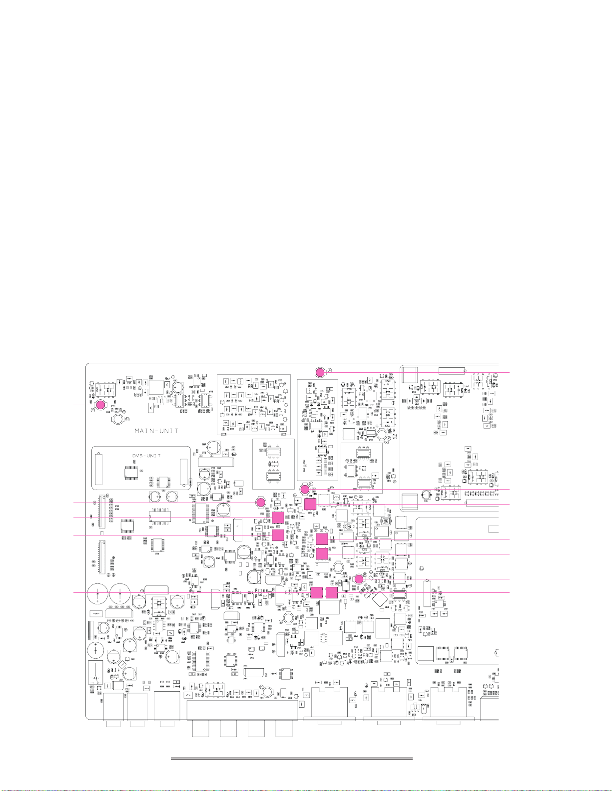
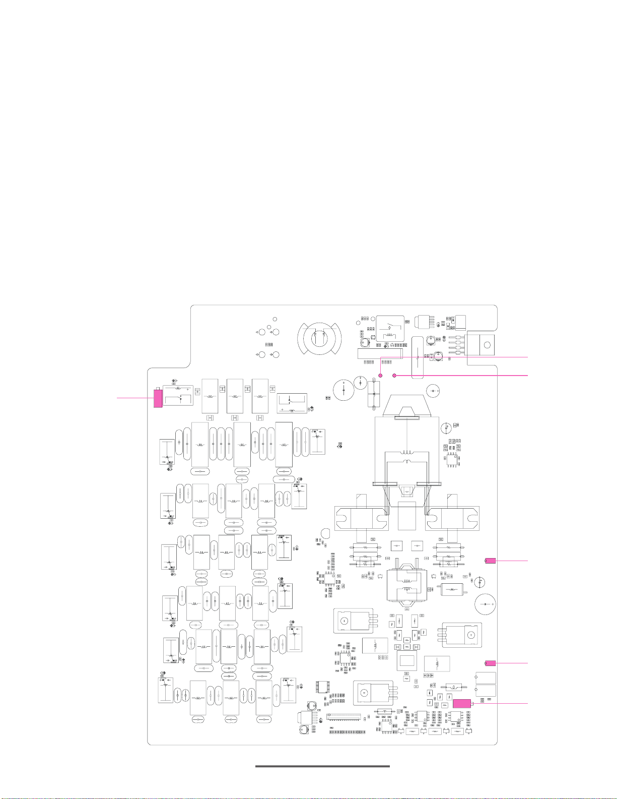
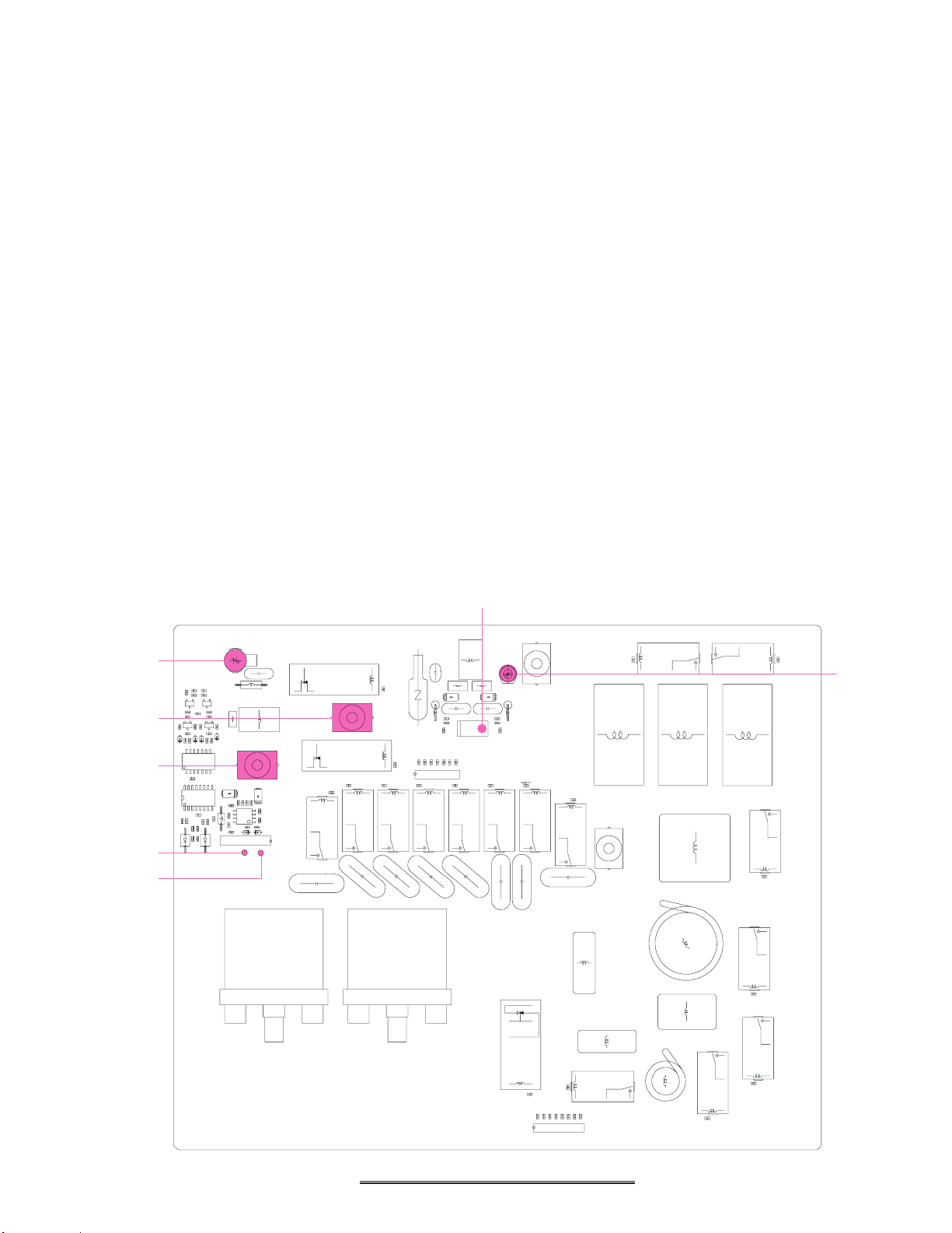
MAIN Unit (Lot. 1)
Provided by
YAESU museum
Downloaded by
RadioAmateur.EU
Circuit Diagram
MAIN-1
Page 38

MAIN Unit (Lot. 1)
Note
MAIN-2
Page 39

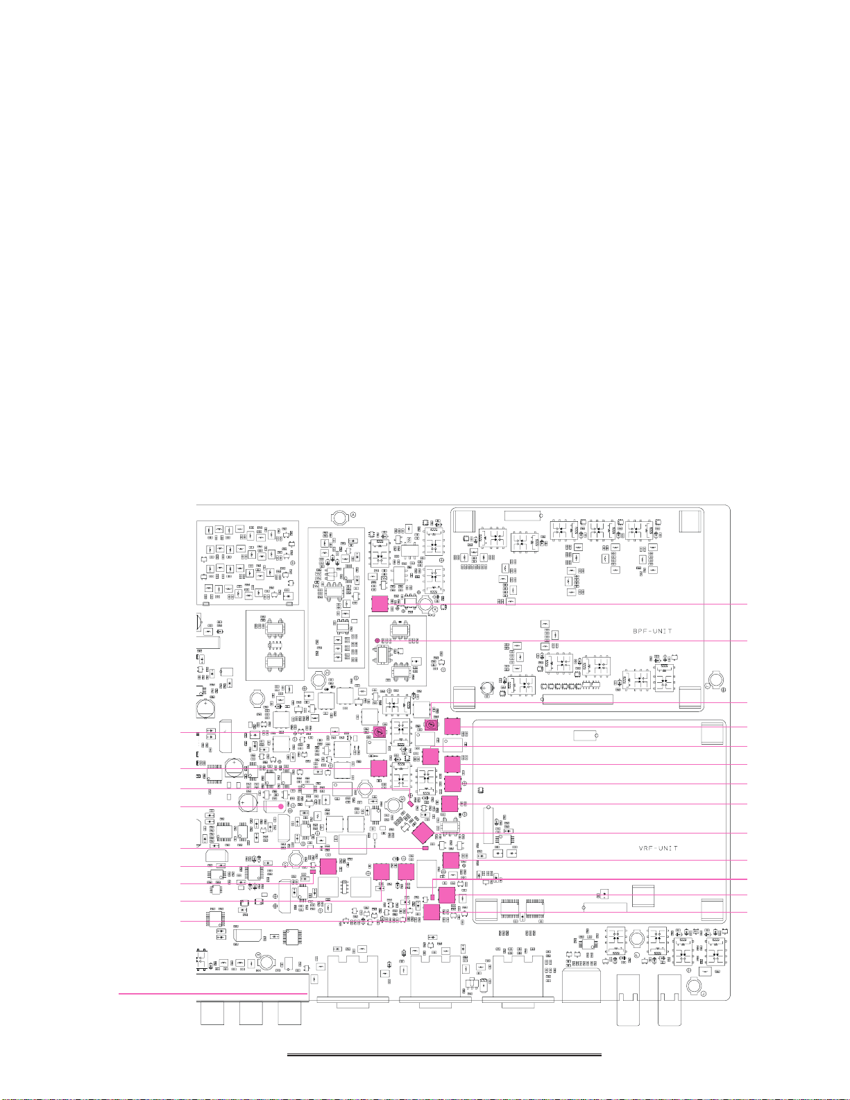
MAIN Unit (Lot. 1)
Parts Layout (Side A)
M62364FP
(Q1021, 1054)
NJU3714A
(Q1005, 1012,
1082, 1097)
SN74HCT244PWR
(Q1018)
M62353AGP
(Q1020)
TC74HC04AF
(Q1111)
2SA1602A (MF)
(Q1040, 1044, 1092)
2SB624 (BV3)
(Q4507)
2SC2714 (QY)
(Q1053, 1103)
2SC3356 (R24)
(Q1029, 1030)
2SC4154 (E)
(Q1013, 1014, 1015,
1016, 1025, 1026,
1033, 1034, 1038,
1048, 1057, 1062,
1065, 1068, 1072,
1087, 1095, 1101,
1106, 1115)
DTC114EUA (24)
(Q1002, 1003,
1004, 1011, 1017,
1019, 1089, 1112)
DTC114YUA (64)
(Q1007, 1009)
DTC144EUA (26)
(Q1035, 1050)
SST310 (Z0)
(Q1023, 1024, 1070,
1093, 1094, 1107)
A B C D E F G H I
1
2
3
CD74HCT4053PWR
(Q1027, 1043, 1059,
1069, 1100)
LA2902PWR
(Q1080, 1099)
HD74LV2G74A (QK)
(Q1056, 1063)
LM2904PWR
(Q1064, 1079, 1083,
1108, 1109, 1110,
1113)
LM4881MX
(Q1088)
NJM2068V
(Q1032, 1074, 1075,
1076, 1077, 1078)
NJM2594V
(Q1081, 1098)
NJM2737V
(Q1090, 1096, 1102)
SN74LVC2G53DCTR
(Q1046)
SN74LVC2G66DCTR
(Q1091)
2SC2945 (QK)
(Q1010, 1103)
2SD2403GY (GY)
(Q1008)
UMD5N
(Q1022, 1031, 1036,
1037, 1039, 1041,
1042, 1045, 1047,
1049, 1052, 1055,
1060, 1061, 1066,
1067, 1071, 1104,
1114)
LA4425A
(Q1086)
SPM5001
(Q1058)
SN74LVC1G66DCKR
(Q1051)
1SS226 (C3)
(D1081)
1SS372 (N9)
(D1054)
HSM198S (C6)
(D1053)
4
5
6
7
3SK131 (V12)
(Q1006)
BB301CAW (AW)
(Q1028, 1073, 1085,
1105)
DAN202U (N)
(D1041, 1042, 1048,)
DAP236U (X)
(D1011, 1012, 1018,
1019, 1045, 1055)
HSB88WSTR
(D1031, 1052)
HZM7.5NB3
(D1027, 1032, 1038)
IMN10
(D1033, 1034)
MAIN-3
Page 40

MAIN Unit (Lot. 1)
Parts Layout (Side A)
a b c d e f g h i
1
2
3
4
5
6
7
MAIN-4
Page 41

MAIN Unit (Lot. 2~5)
Provided by
YAESU museum
Downloaded by
RadioAmateur.EU
Circuit Diagram
MAIN-5
Page 42

MAIN Unit (Lot. 2~5)
Note
MAIN-6
Page 43

MAIN Unit (Lot. 2~5)
Parts Layout (Side A)
M62364FP
(Q1021, 1054)
NJU3714A
(Q1005, 1012,
1082, 1097)
SN74HCT244PWR
(Q1018)
M62353AGP
(Q1020)
TC74HC04AF
(Q1111)
2SA1602A (MF)
(Q1040, 1044, 1092)
2SB624 (BV3)
(Q4507)
2SC2714 (QY)
(Q1053, 1103)
2SC3356 (R24)
(Q1029, 1030)
2SC4154 (E)
(Q1013, 1014, 1015,
1016, 1025, 1026,
1033, 1034, 1038,
1048, 1057, 1062,
1065, 1068, 1072,
1087, 1095, 1101,
1106, 1115)
DTC114EUA (24)
(Q1002, 1003,
1004, 1011, 1017,
1019, 1089, 1112)
DTC114YUA (64)
(Q1007, 1009)
DTC144EUA (26)
(Q1035, 1050)
SST310 (Z0)
(Q1023, 1024, 1070,
1093, 1094, 1107)
A B C D E F G H I
1
2
3
CD74HCT4053PWR
(Q1027, 1043, 1059,
1069, 1100)
LA2902PWR
(Q1080, 1099)
HD74LV2G74A (QK)
(Q1056, 1063)
LM2904PWR
(Q1064, 1079, 1083,
1108, 1109, 1110,
1113)
LM4881MX
(Q1088)
NJM2068V
(Q1032, 1074, 1075,
1076, 1077, 1078)
NJM2594V
(Q1081, 1098)
NJM2737V
(Q1090, 1096, 1102)
SN74LVC2G53DCTR
(Q1046)
SN74LVC2G66DCTR
(Q1091)
2SC2945 (QK)
(Q1010, 1103)
2SD2403GY (GY)
(Q1008)
UMD5N
(Q1022, 1031, 1036,
1037, 1039, 1041,
1042, 1045, 1047,
1049, 1052, 1055,
1060, 1061, 1066,
1067, 1071, 1104,
1114)
LA4425A
(Q1086)
SPM5001
(Q1058)
SN74LVC1G66DCKR
(Q1051)
1SS226 (C3)
(D1081)
1SS372 (N9)
(D1054)
HSM198S (C6)
(D1053)
4
5
6
7
3SK131 (V12)
(Q1006)
BB301CAW (AW)
(Q1028, 1073, 1085,
1105)
DAN202U (N)
(D1041, 1042, 1048,)
DAP236U (X)
(D1011, 1012, 1018,
1019, 1045, 1055)
HSB88WSTR
(D1031, 1052)
HZM7.5NB3
(D1027, 1032, 1038)
IMN10
(D1033, 1034)
MAIN-7
Page 44

MAIN Unit (Lot. 2~5)
Parts Layout (Side A)
a b c d e f g h i
1
2
3
4
5
6
7
MAIN-8
Page 45

MAIN Unit (Lot. 6~)
Provided by
YAESU museum
Downloaded by
RadioAmateur.EU
Circuit Diagram
MAIN-9
Page 46

MAIN Unit (Lot. 6~)
Note
MAIN-10
Page 47

MAIN Unit (Lot. 6~)
Parts Layout (Side A)
M62364FP
(Q1021, 1054)
NJU3714A
(Q1005, 1012,
1082, 1097)
SN74HCT244PWR
(Q1018)
M62353AGP
(Q1020)
TC74HC04AF
(Q1111)
2SA1602A (MF)
(Q1040, 1044, 1092)
2SB624 (BV3)
(Q4507)
2SC2714 (QY)
(Q1053, 1103)
2SC3356 (R24)
(Q1029, 1030)
2SC4154 (E)
(Q1013, 1014, 1015,
1016, 1025, 1026,
1033, 1034, 1038,
1048, 1057, 1062,
1065, 1068, 1072,
1087, 1095, 1101,
1106, 1115)
DTC114EUA (24)
(Q1002, 1003,
1004, 1011, 1017,
1019, 1089, 1112)
DTC114YUA (64)
(Q1007, 1009)
DTC144EUA (26)
(Q1035, 1050)
SST310 (Z0)
(Q1023, 1024, 1070,
1093, 1094, 1107)
A B C D E F G H I
1
2
3
CD74HCT4053PWR
(Q1027, 1043, 1059,
1069, 1100)
LA2902PWR
(Q1080, 1099)
HD74LV2G74A (QK)
(Q1056, 1063)
LM2904PWR
(Q1064, 1079, 1083,
1108, 1109, 1110,
1113)
LM4881MX
(Q1088)
NJM2068V
(Q1032, 1074, 1075,
1076, 1077, 1078)
NJM2594V
(Q1081, 1098)
NJM2737V
(Q1090, 1096, 1102)
SN74LVC2G53DCTR
(Q1046)
SN74LVC2G66DCTR
(Q1091)
2SC2945 (QK)
(Q1010, 1103)
2SD2403GY (GY)
(Q1008)
UMD5N
(Q1022, 1031, 1036,
1037, 1039, 1041,
1042, 1045, 1047,
1049, 1052, 1055,
1060, 1061, 1066,
1067, 1071, 1104,
1114)
LA4425A
(Q1086)
SPM5001
(Q1058)
SN74LVC1G66DCKR
(Q1051)
1SS226 (C3)
(D1081)
1SS372 (N9)
(D1054)
HSM198S (C6)
(D1053)
4
5
6
7
3SK131 (V12)
(Q1006)
BB301CAW (AW)
(Q1028, 1073, 1085,
1105)
DAN202U (N)
(D1041, 1042, 1048,)
DAP236U (X)
(D1011, 1012, 1018,
1019, 1045, 1055)
HSB88WSTR
(D1031, 1052)
HZM7.5NB3
(D1027, 1032, 1038)
IMN10
(D1033, 1034)
MAIN-11
Page 48

MAIN Unit (Lot. 6~)
Parts Layout (Side A)
a b c d e f g h i
1
2
3
4
5
6
7
MAIN-12
Page 49

MAIN Unit
Parts List
REF DESCRIPTION VALUE V/W TOL. MFR'S DESIG VXSTD P/N VERS.
PCB with Components CB3483001
Printed Circuit Board FR014590B 1
FR014590C 2-
FR014590D 6C 1001 CHIP CAP. 0.01uF 50V B GRM188B11H103KA01D K22174823 1- A C6
C 1002 CHIP CAP. 0.01uF 50V B GRM188B11H103KA01D K22174823 1- A G6
C 1003 CHIP CAP. 0.001uF 50V B GRM188B11H102KA01D K22174821 1- A C6
C 1004 CHIP CAP. 0.001uF 50V B GRM188B11H102KA01D K22174821 1- A G6
C 1005 CHIP CAP. 0.001uF 50V B GRM188B11H102KA01D K22174821 1- A G6
C 1006 CHIP CAP. 0.01uF 50V B GRM188B11H103KA01D K22174823 1- A B6
C 1007 CHIP CAP. 0.001uF 50V B GRM188B11H102KA01D K22174821 1- A C6
C 1008 CHIP CAP. 100pF 50V CH GRM1882C1H101JA01D K22174235 1- A G6
C 1009 CHIP CAP. 0.1uF 16V B GRM188B11C104KA01D K22124805 1- A A3
C 1010 CHIP CAP. 0.01uF 50V B GRM188B11H103KA01D K22174823 1- A A1
C 1011 CHIP CAP. 220pF 50V CH GRM1882C1H221JA01D K22174243 1- A C6
C 1012 CHIP CAP. 68pF 50V CH GRM1882C1H680JA01D K22174231 1- A A1
C 1013 CHIP CAP. 0.001uF 50V B GRM188B11H102KA01D K22174821 1- A G6
C 1014 CHIP CAP. 12pF 50V CH GRM1882C1H120JA01D K22174213 1- A A1
C 1015 CHIP CAP. 0.01uF 50V B GRM188B11H103KA01D K22174823 1- A A1
C 1016 CHIP CAP. 0.1uF 16V B GRM188B11C104KA01D K22124805 1- A A3
C 1017 CHIP CAP. 0.01uF 50V B GRM188B11H103KA01D K22174823 1- A I6
C 1018 CHIP CAP. 220pF 50V CH GRM1882C1H221JA01D K22174243 1- A C6
C 1019 CHIP CAP. 100pF 50V CH GRM1882C1H101JA01D K22174235 1- A A1
C 1020 CHIP CAP. 100pF 50V CH GRM1882C1H101JA01D K22174235 1- A G6
C 1021 CHIP CAP. 33pF 50V CH GRM1882C1H330JA01D K22174223 1- A A1
C 1022 CHIP CAP. 0.01uF 50V B GRM188B11H103KA01D K22174823 1- A B6
C 1023 CHIP CAP. 0.01uF 50V B GRM188B11H103KA01D K22174823 1- A B6
C 1024 CHIP CAP. 0.001uF 50V B GRM188B11H102KA01D K22174821 1- A G6
C 1025 CHIP CAP. 0.001uF 50V B GRM188B11H102KA01D K22174821 1- A G6
C 1026 CHIP CAP. 68pF 50V CH GRM1882C1H680JA01D K22174231 1- A A1
C 1027 CHIP CAP. 82pF 50V CH GRM1882C1H820JA01D K22174233 1- A A1
C 1028 CHIP TA.CAP. 10uF 16V TEMSVB21C106M-8R K78120025 1- A B6
C 1029 CHIP CAP. 0.001uF 50V B GRM188B11H102KA01D K22174821 1- A G6
C 1030 CHIP CAP. 0.01uF 50V B GRM188B11H103KA01D K22174823 1- A A1
C 1031 CHIP CAP. 0.001uF 50V B GRM188B11H102KA01D K22174821 1- A G6
C 1032 CHIP CAP. 0.001uF 50V B GRM188B11H102KA01D K22174821 1- A G6
C 1033 CHIP CAP. 0.01uF 50V B GRM188B11H103KA01D K22174823 1- A B6
C 1034 CHIP CAP. 0.1uF 16V B GRM188B11C104KA01D K22124805 1- A B1
C 1035 CHIP CAP. 33pF 50V CH GRM1882C1H330JA01D K22174223 1- A A1
C 1036 CHIP CAP. 0.01uF 50V B GRM188B11H103KA01D K22174823 1- A I6
C 1037 CHIP CAP. 0.01uF 50V B GRM188B11H103KA01D K22174823 1- A A1
C 1038 CHIP CAP. 100pF 50V CH GRM1882C1H101JA01D K22174235 1- A G6
C 1039 CHIP CAP. 0.01uF 50V B GRM188B11H103KA01D K22174823 1- A B1
C 1040 CHIP CAP. 0.1uF 16V B GRM188B11C104KA01D K22124805 1- A B1
C 1041 CHIP CAP. 0.001uF 50V B GRM188B11H102KA01D K22174821 1- A G6
C 1042 CHIP TA.CAP. 10uF 16V TEMSVB21C106M-8R K78120025 1- A B1
C 1043 CHIP CAP. 220pF 50V CH GRM1882C1H221JA01D K22174243 1- A F6
C 1044 CHIP CAP. 0.1uF 16V B GRM188B11C104KA01D K22124805 1- A B1
C 1045 CHIP CAP. 0.1uF 16V B GRM188B11C104KA01D K22124805 1- A B4
C 1046 CHIP CAP. 1uF 6.3V B GRM188B10J105KA01D K22084801 1- A B1
C 1047 CHIP CAP. 100pF 50V CH GRM1882C1H101JA01D K22174235 1- A G6
C 1048 CHIP CAP. 0.1uF 16V B GRM188B11C104KA01D K22124805 1- A A1
C 1049 CHIP CAP. 0.01uF 50V B GRM188B11H103KA01D K22174823 1- A B1
C 1050 CHIP CAP. 0.01uF 50V B GRM188B11H103KA01D K22174823 1- A F6
C 1051 CHIP CAP. 0.01uF 50V B GRM188B11H103KA01D K22174823 1- A B1
C 1052 CHIP CAP. 0.01uF 50V B GRM188B11H103KA01D K22174823 1- A A1
C 1053 CHIP CAP. 0.01uF 50V B GRM188B11H103KA01D K22174823 1- A I6
C 1054 CHIP CAP. 220pF 50V CH GRM1882C1H221JA01D K22174243 1- A F6
C 1055 CHIP CAP. 0.1uF 16V B GRM188B11C104KA01D K22124805 1- A B1
C 1056 CHIP CAP. 0.1uF 16V B GRM188B11C104KA01D K22124805 1- A B1
C 1057 CHIP CAP. 270pF 50V CH GRM1882C1H271JA01D K22174251 1- A B1
C 1058 CHIP CAP. 0.01uF 50V B GRM188B11H103KA01D K22174823 1- A B1
C 1059 CHIP CAP. 0.01uF 50V B GRM188B11H103KA01D K22174823 1- A B1
C 1060 CHIP CAP. 0.01uF 50V B GRM188B11H103KA01D K22174823 1- A I6
C 1061 CHIP CAP. 270pF 50V CH GRM1882C1H271JA01D K22174251 1- A B1
C 1062 CHIP CAP. 0.1uF 16V B GRM188B11C104KA01D K22124805 1- A B1
C 1063 CHIP TA.CAP. 10uF 16V TEMSVB21C106M-8R K78120025 1- A H5
C 1064 CHIP CAP. 0.01uF 50V B GRM188B11H103KA01D K22174823 1- A C1
C 1065 CHIP CAP. 0.01uF 50V B GRM188B11H103KA01D K22174823 1- A H5
C 1066 CHIP CAP. 0.01uF 50V B GRM188B11H103KA01D K22174823 1- A B1
C 1067 CHIP CAP. 0.1uF 16V B GRM188B11C104KA01D K22124805 1- A B1
C 1068 CHIP CAP. 0.1uF 16V B GRM188B11C104KA01D K22124805 1- A C1
C 1069 AL.ELECTRO.CAP. 22uF 16V EEE1CA220SR K48120024 1- A B1
LOT
SIDE
LAY ADR
MAIN-13
Page 50

MAIN Unit
Parts List
REF DESCRIPTION VALUE V/W TOL. MFR'S DESIG VXSTD P/N VERS.
C 1070 CHIP CAP. 0.01uF 50V B GRM188B11H103KA01D K22174823 1- A G6
C 1071 CHIP CAP. 56pF 50V CH GRM1882C1H560JA01D K22174229 1- A C1
C 1072 CHIP CAP. 120pF 50V CH GRM1882C1H121JA01D K22174237 1- A C1
C 1073 CHIP CAP. 0.01uF 50V B GRM188B11H103KA01D K22174823 1- A D2
C 1074 CHIP CAP. 56pF 50V CH GRM1882C1H560JA01D K22174229 1- A C1
C 1075 CHIP TA.CAP. 10uF 16V TEMSVB21C106M-8R K78120025 1- A D2
C 1076 CHIP CAP. 120pF 50V CH GRM1882C1H121JA01D K22174237 1- A C1
C 1077 CHIP CAP. 510pF 50V CH GRM1882C1H511JA01D K22174257 1- A C1
C 1078 CHIP CAP. 0.01uF 50V B GRM188B11H103KA01D K22174823 1- A H6
C 1079 CHIP CAP. 220pF 50V CH GRM1882C1H221JA01D K22174243 1- A C1
C 1080 CHIP CAP. 56pF 50V CH GRM1882C1H560JA01D K22174229 1- A C2
C 1081 CHIP CAP. 0.01uF 50V B GRM188B11H103KA01D K22174823 1- A H6
C 1082 CHIP CAP. 0.01uF 50V B GRM188B11H103KA01D K22174823 1- A H6
C 1083 CHIP CAP. 120pF 50V CH GRM1882C1H121JA01D K22174237 1- A C1
C 1084 CHIP CAP. 510pF 50V CH GRM1882C1H511JA01D K22174257 1- A C1
C 1085 CHIP CAP. 220pF 50V CH GRM1882C1H221JA01D K22174243 1- A C1
C 1086 CHIP CAP. 100pF 50V CH GRM1882C1H101JA01D K22174235 1- A C2
C 1087 CHIP CAP. 56pF 50V CH GRM1882C1H560JA01D K22174229 1- A C1
C 1088 CHIP CAP. 120pF 50V CH GRM1882C1H121JA01D K22174237 1- A C1
C 1089 CHIP CAP. 56pF 50V CH GRM1882C1H560JA01D K22174229 1- A C1
C 1090 CHIP CAP. 0.01uF 50V B GRM188B11H103KA01D K22174823 1- A C1
C 1091 CHIP CAP. 82pF 50V CH GRM1882C1H820JA01D K22174233 1- A C2
C 1092 CHIP CAP. 0.1uF 16V B GRM188B11C104KA01D K22124805 1- A C1
C 1093 CHIP CAP. 150pF 50V CH GRM1882C1H151JA01D K22174239 1- A C1
C 1094 CHIP CAP. 0.0027uF 50V B GRM188B11H272KA01D K22174829 1- A C1
C 1095 CHIP CAP. 0.033uF 16V R GRM188R11C333KA01D K22124801 1- A C1
C 1096 CHIP CAP. 0.1uF 16V B GRM188B11C104KA01D K22124805 1- A C1
C 1097 CHIP CAP. 0.01uF 50V B GRM188B11H103KA01D K22174823 1- A C2
C 1098 CHIP CAP. 0.1uF 16V B GRM188B11C104KA01D K22124805 1- A C1
C 1099 CHIP CAP. 330pF 50V CH GRM1882C1H331JA01D K22174253 1- A C1
C 1100 CHIP CAP. 68pF 50V CH GRM1882C1H680JA01D K22174231 1- A C1
C 1101 CHIP CAP. 0.01uF 50V B GRM188B11H103KA01D K22174823 1- A H6
C 1102 CHIP CAP. 0.1uF 16V B GRM188B11C104KA01D K22124805 1- A C1
C 1103 CHIP CAP. 100pF 50V CH GRM1882C1H101JA01D K22174235 1- A C1
C 1104 CHIP CAP. 0.1uF 16V B GRM188B11C104KA01D K22124805 1- A C2
C 1105 CHIP TA.CAP. 1.5uF 16V TESVA1C155M1-8R K78120020 1- A B4
C 1106 CHIP CAP. 0.0018uF 50V B GRM188B11H182KA01D K22174828 1- A C1
C 1107 CHIP CAP. 220pF 50V CH GRM1882C1H221JA01D K22174243 1- A C1
C 1108 CHIP CAP. 33pF 50V CH GRM1882C1H330JA01D K22174223 1- A C2
C 1109 CHIP CAP. 150pF 50V CH GRM1882C1H151JA01D K22174239 1- A D1
C 1110 CHIP CAP. 0.0027uF 50V B GRM188B11H272KA01D K22174829 1- A D1
C 1111 CHIP CAP. 47pF 50V CH GRM1882C1H470JA01D K22174227 1- A F2
C 1112 CHIP CAP. 330pF 50V CH GRM1882C1H331JA01D K22174253 1- A D1
C 1113 CHIP CAP. 68pF 50V CH GRM1882C1H680JA01D K22174231 1- A C1
C 1114 CHIP CAP. 0.01uF 50V B GRM188B11H103KA01D K22174823 1- A D1
C 1115 CHIP CAP. 0.1uF 16V B GRM188B11C104KA01D K22124805 1- A D1
C 1116 CHIP CAP. 0.033uF 16V R GRM188R11C333KA01D K22124801 1- A D1
C 1117 CHIP CAP. 0.01uF 50V B GRM188B11H103KA01D K22174823 1- A D2
C 1118 AL.ELECTRO.CAP. 47uF 16V EEE1CA470WR K48120025 1- A B3
C 1119 CHIP CAP. 82pF 50V CH GRM1882C1H820JA01D K22174233 1- A F2
C 1120 AL.ELECTRO.CAP. 47uF 16V EEE1CA470WR K48120025 1- A B3
C 1121 CHIP CAP. 0.1uF 16V B GRM188B11C104KA01D K22124805 1- A B2
C 1122 AL.ELECTRO.CAP. 47uF 16V EEE1CA470SP K48120005 1- A C4
C 1123 CHIP CAP. 47pF 50V CH GRM1882C1H470JA01D K22174227 1- A F1
C 1124 CHIP CAP. 0.01uF 50V B GRM188B11H103KA01D K22174823 1- A C2
C 1125 AL.ELECTRO.CAP. 47uF 16V EEE1CA470SP K48120005 1- A C4
C 1126 CHIP CAP. 82pF 50V CH GRM1882C1H820JA01D K22174233 1- A G1
C 1127 CHIP CAP. 0.01uF 50V B GRM188B11H103KA01D K22174823 1- A G2
C 1128 CHIP CAP. 0.01uF 50V B GRM188B11H103KA01D K22174823 1- A G1
C 1129 CHIP CAP. 0.01uF 50V B GRM188B11H103KA01D K22174823 1- A H1
C 1130 CHIP CAP. 0.01uF 50V B GRM188B11H103KA01D K22174823 1- A H1
C 1131 CHIP CAP. 0.01uF 50V B GRM188B11H103KA01D K22174823 1- A F3
C 1132 CHIP CAP. 0.1uF 16V B GRM188B11C104KA01D K22124805 1- A C2
C 1133 CHIP CAP. 0.01uF 50V B GRM188B11H103KA01D K22174823 1- A H3
C 1134 CHIP CAP. 0.01uF 50V B GRM188B11H103KA01D K22174823 1- A G2
C 1135 CHIP CAP. 39pF 50V CH GRM1882C1H390JA01D K22174225 1- A G1
C 1136 CHIP CAP. 0.1uF 16V B GRM188B11C104KA01D K22124805 1- A C4
C 1137 CHIP CAP. 100pF 50V CH GRM1882C1H101JA01D K22174235 1- A F4
C 1138 CHIP CAP. 0.01uF 50V B GRM188B11H103KA01D K22174823 1- A F1
C 1139 CHIP CAP. 0.01uF 50V B GRM188B11H103KA01D K22174823 1- A G1
C 1140 CHIP CAP. 82pF 50V CH GRM1882C1H820JA01D K22174233 1- A G2
C 1141 CHIP CAP. 82pF 50V CH GRM1882C1H820JA01D K22174233 1- A G1
C 1142 CHIP CAP. 0.001uF 25V CH GRM1882C1E102JA01D K22144204 1- A F2
LOT
SIDE
LAY ADR
MAIN-14
Page 51

MAIN Unit
Parts List
REF DESCRIPTION VALUE V/W TOL. MFR'S DESIG VXSTD P/N VERS.
C 1143 CHIP CAP. 180pF 50V CH GRM1882C1H181JA01D K22174241 1- A G1
C 1144 CHIP CAP. 0.001uF 25V CH GRM1882C1E102JA01D K22144204 1- A H1
C 1145 CHIP CAP. 150pF 50V CH GRM1882C1H151JA01D K22174239 1- A G2
C 1146 CHIP CAP. 0.0056uF 50V B GRM188B11H562KA01D K22174818 1- A G2
C 1147 CHIP CAP. 180pF 50V CH GRM1882C1H181JA01D K22174241 1- A G1
C 1148 CHIP CAP. 100pF 50V CH GRM1882C1H101JA01D K22174235 1- A D4
C 1149 CHIP CAP. 0.0018uF 50V B GRM188B11H182KA01D K22174812 1- A H1
C 1150 CHIP CAP. 100pF 50V CH GRM1882C1H101JA01D K22174235 1- A D4
C 1151 CHIP CAP. 430pF 50V CH GRM1882C1H431JA01D K22174256 1- A H1
C 1152 CHIP CAP. 0.0056uF 50V B GRM188B11H562KA01D K22174818 1- A G2
C 1153 CHIP CAP. 39pF 50V CH GRM1882C1H390JA01D K22174225 1- A G2
C 1154 CHIP CAP. 82pF 50V CH GRM1882C1H820JA01D K22174233 1- A G1
C 1155 CHIP CAP. 180pF 50V CH GRM1882C1H181JA01D K22174241 1- A G1
C 1156 CHIP CAP. 0.0056uF 50V B GRM188B11H562KA01D K22174818 1- A H1
C 1157 CHIP CAP. 0.01uF 50V B GRM188B11H103KA01D K22174823 1- A F5
C 1158 CHIP CAP. 0.001uF 25V CH GRM1882C1E102JA01D K22144204 1- A F2
C 1159 CHIP CAP. 82pF 50V CH GRM1882C1H820JA01D K22174233 1- A G1
C 1160 CHIP CAP. 0.001uF 25V CH GRM1882C1E102JA01D K22144204 1- A H1
C 1161 CHIP CAP. 150pF 50V CH GRM1882C1H151JA01D K22174239 1- A G2
C 1162 CHIP CAP. 39pF 50V CH GRM1882C1H390JA01D K22174225 1- A D3
C 1163 CHIP CAP. 0.1uF 16V B GRM188B11C104KA01D K22124805 1- A D3
C 1164 CHIP CAP. 8pF 50V CH GRM1882C1H8R0DZ01D K22174209 1- A D3
C 1165 CHIP CAP. 180pF 50V CH GRM1882C1H181JA01D K22174241 1- A G1
C 1166 CHIP CAP. 0.0018uF 50V B GRM188B11H182KA01D K22174812 1- A H1
C 1167 CHIP TA.CAP. 1uF 35V TEMSVA1V105M-8R K78160032 1- A B3
C 1168 CHIP TA.CAP. 1uF 35V TEMSVA1V105M-8R K78160032 1- A B3
C 1169 CHIP CAP. 47pF 50V CH GRM1882C1H470JA01D K22174227 1- A F1
C 1170 CHIP CAP. 6pF 50V CH GRM1882C1H6R0DZ01D K22174207 1- A F1
C 1171 CHIP CAP. 0.01uF 50V B GRM188B11H103KA01D K22174823 1- A D3
C 1172 CHIP CAP. 82pF 50V CH GRM1882C1H820JA01D K22174233 1- A D3
C 1174 CHIP CAP. 82pF 50V CH GRM1882C1H820JA01D K22174233 1- A F1
C 1175 CHIP CAP. 18pF 50V CH GRM1882C1H180JA01D K22174217 1- A F1
C 1176 CHIP CAP. 0.001uF 50V B GRM188B11H102KA01D K22174821 1- A D3
C 1177 CHIP CAP. 39pF 50V CH GRM1882C1H390JA01D K22174225 1- A D3
C 1178 CHIP CAP. 68pF 50V CH GRM1882C1H680JA01D K22174231 1- A F1
C 1179 CHIP CAP. 27pF 50V CH GRM1882C1H270JA01D K22174221 1- A F1
C 1180 CHIP CAP. 47pF 50V CH GRM1882C1H470JA01D K22174227 1- A D4
C 1181 CHIP TA.CAP. 10uF 16V TEESVA1C106M8R K78120077 1- A B4
C 1182 CHIP CAP. 47pF 50V CH GRM1882C1H470JA01D K22174227 1- A D4
C 1183 AL.ELECTRO.CAP. 22uF 16V EEE1CA220SR K48120024 1- A C4
C 1184 CHIP CAP. 27pF 50V CH GRM1882C1H270JA01D K22174221 1- A F1
C 1185 CHIP CAP. 15pF 50V CH GRM1882C1H150JA01D K22174215 1- A D3
C 1186 CHIP CAP. 0.01uF 50V B GRM188B11H103KA01D K22174823 1- A D3
C 1187 AL.ELECTRO.CAP. 220uF 10V RV3-10V221MF80-R K48100002 1- A C3
C 1188 CHIP CAP. 0.001uF 50V B GRM188B11H102KA01D K22174821 1- A D6
C 1189 CHIP TA.CAP. 1uF 35V TEMSVA1V105M-8R K78160032 1- A B5
C 1190 CHIP TA.CAP. 10uF 16V TEMSVB21C106M-8R K78120025 1- A D3
C 1191 CHIP CAP. 0.01uF 50V B GRM188B11H103KA01D K22174823 1- A D3
C 1192 CHIP CAP. 0.0022uF 50V B GRM188B11H222KA01D K22174822 1- A C4
C 1193 CHIP CAP. 47pF 50V CH GRM1882C1H470JA01D K22174227 1- A D4
C 1194 CHIP TA.CAP. 1uF 35V TEMSVA1V105M-8R K78160032 1- A C3
C 1195 CHIP CAP. 0.001uF 50V B GRM188B11H102KA01D K22174821 1- A D3
C 1196 CHIP CAP. 0.0047uF 50V B GRM188B11H472KA01D K22174833 1- A C4
C 1197 CHIP CAP. 0.01uF 50V B GRM188B11H103KA01D K22174823 1- A D3
C 1198 CHIP CAP. 0.1uF 16V B GRM188B11C104KA01D K22124805 1- A D4
C 1199 CHIP CAP. 0.01uF 50V B GRM188B11H103KA01D K22174823 1- A D6
C 1200 CHIP TA.CAP. 10uF 16V TEMSVB21C106M-8R K78120025 1- A D4
C 1201 CHIP CAP. 220pF 50V CH GRM1882C1H221JA01D K22174243 1- A D4
C 1202 AL.ELECTRO.CAP. 220uF 16V MVA16VC220MF80 K48120021 1- A B3
C 1203 CHIP CAP. 10pF 50V CH GRM1882C1H100JA01D K22174211 1- A D3
C 1204 AL.ELECTRO.CAP. 47uF 16V EEE1CA470WR K48120025 1- A C2
C 1205 CHIP CAP. 0.01uF 50V B GRM188B11H103JA01D K22174824 1- A F1
C 1206 CHIP CAP. 0.047uF 16V B GRM39B473K16PT K22124804 1- A B5
C 1207 CHIP TA.CAP. 1uF 35V TEMSVA1V105M-8R K78160032 1- A C3
C 1208 CHIP CAP. 47pF 50V CH GRM1882C1H470JA01D K22174227 1- A D4
C 1209 CHIP CAP. 0.001uF 50V B GRM188B11H102KA01D K22174821 1- A C3
C 1210 CHIP CAP. 0.01uF 50V B GRM188B11H103KA01D K22174823 1- A D3
C 1211 CHIP CAP. 0.1uF 16V B GRM188B11C104KA01D K22124805 1- A E1
C 1212 CHIP CAP. 0.001uF 50V B GRM188B11H102KA01D K22174821 1- A E1
C 1213 CHIP CAP. 0.1uF 16V B GRM188B11C104KA01D K22124805 1- A E1
C 1214 CHIP CAP. 0.001uF 50V B GRM188B11H102KA01D K22174821 1- A E1
C 1215 CHIP CAP. 18pF 50V CH GRM1882C1H180JA01D K22174217 1- A D3
C 1216 CHIP CAP. 0.01uF 50V B GRM188B11H103KA01D K22174823 1- A D3
LOT
SIDE
LAY ADR
MAIN-15
Page 52

MAIN Unit
Parts List
REF DESCRIPTION VALUE V/W TOL. MFR'S DESIG VXSTD P/N VERS.
C 1217 CHIP CAP. 0.1uF 16V B GRM188B11C104KA01D K22124805 1- A B5
C 1218 CHIP CAP. 0.022uF 50V B GRM40B223M50PT K22170821 1- A D5
C 1219 CHIP CAP. 0.1uF 16V B GRM188B11C104KA01D K22124805 1- A E1
C 1220 CHIP CAP. 0.1uF 16V B GRM188B11C104KA01D K22124805 1- A E1
C 1221 CHIP CAP. 0.001uF 50V B GRM188B11H102KA01D K22174821 1- A C3
C 1222 CHIP TA.CAP. 1uF 35V TEMSVA1V105M-8R K78160032 1- A C2
C 1223 CHIP CAP. 56pF 50V CH GRM1882C1H560JA01D K22174229 1- A D5
C 1224 CHIP CAP. 0.01uF 50V B GRM188B11H103KA01D K22174823 1- A C3
C 1225 CHIP CAP. 0.001uF 50V B GRM188B11H102KA01D K22174821 1- A E1
C 1226 CHIP CAP. 0.001uF 50V B GRM188B11H102KA01D K22174821 1- A E2
C 1227 CHIP CAP. 0.001uF 50V B GRM188B11H102KA01D K22174821 1- A E1
C 1228 CHIP CAP. 0.001uF 50V B GRM188B11H102KA01D K22174821 1- A E2
C 1229 CHIP CAP. 0.1uF 16V B GRM188B11C104KA01D K22124805 1- A E1
C 1230 CHIP CAP. 0.1uF 16V B GRM188B11C104KA01D K22124805 1- A E1
C 1231 CHIP CAP. 0.01uF 50V B GRM188B11H103KA01D K22174823 1- A D3
C 1232 CHIP CAP. 10pF 50V CH GRM1882C1H100JA01D K22174211 1- A D3
C 1233 CHIP CAP. 0.001uF 50V B GRM188B11H102KA01D K22174821 1- A C2
C 1234 CHIP TA.CAP. 1uF 35V TEMSVA1V105M-8R K78160032 1- A C3
C 1235 CHIP TA.CAP. 1uF 35V TEMSVA1V105M-8R K78160032 1- A C3
C 1236 CHIP CAP. 0.01uF 50V B GRM188B11H103KA01D K22174823 1- A C2
C 1237 CHIP CAP. 0.1uF 16V B GRM188B11C104KA01D K22124805 1- A E1
C 1238 CHIP CAP. 0.1uF 16V B GRM188B11C104KA01D K22124805 1- A E2
C 1239 CHIP CAP. 15pF 50V CH GRM1882C1H150JA01D K22174215 1- A D3
C 1240 CHIP TA.CAP. 1uF 35V TEMSVA1V105M-8R K78160032 1- A D4
C 1241 CHIP CAP. 0.01uF 50V B GRM188B11H103KA01D K22174823 1- A C2
C 1242 CHIP CAP. 0.1uF 16V B GRM188B11C104KA01D K22124805 1- A E1
C 1243 CHIP CAP. 0.1uF 16V B GRM188B11C104KA01D K22124805 1- A E2
C 1244 CHIP TA.CAP. 10uF 16V TEESVA1C106M8R K78120077 1- A D5
C 1245 CHIP CAP. 0.047uF 16V B GRM39B473K16PT K22124804 1- A B5
C 1246 CHIP CAP. 0.001uF 50V B GRM188B11H102KA01D K22174821 1- A C2
C 1247 CHIP TA.CAP. 0.22uF 35V TESVA1V224M1-8R K78160027 1- A D3
C 1248 CHIP TA.CAP. 10uF 16V TEESVA1C106M8R K78120077 1- A D5
C 1249 CHIP CAP. 0.0022uF 50V B GRM188B11H222KA01D K22174822 1- A E6
C 1250 CHIP CAP. 0.01uF 50V B GRM188B11H103KA01D K22174823 1- A D4
C 1251 CHIP CAP. 0.1uF 16V B GRM188B11C104KA01D K22124805 1- A C5
C 1252 CHIP CAP. 0.1uF 16V B GRM188B11C104KA01D K22124805 1- A C3
C 1253 CHIP TA.CAP. 0.47uF 35V TEMSVA1V474M-8R K78160029 1- A C3
C 1254 CHIP TA.CAP. 10uF 16V TEMSVB21C106M-8R K78120025 1- A C3
C 1255 CHIP CAP. 22pF 50V CH GRM1882C1H220JA01D K22174219 1- A C5
C 1256 CHIP CAP. 0.01uF 50V B GRM188B11H103KA01D K22174823 1- A D3
C 1257 CHIP TA.CAP. 10uF 16V TEESVA1C106M8R K78120077 1- A E5
C 1258 CHIP CAP. 0.0022uF 50V B GRM188B11H222KA01D K22174822 1- A E6
C 1259 CHIP CAP. 100pF 50V CH GRM1882C1H101JA01D K22174235 1- A D5
C 1260 CHIP CAP. 330pF 50V CH GRM1882C1H331JA01D K22174253 1- A D5
C 1261 CHIP CAP. 330pF 50V CH GRM1882C1H331JA01D K22174253 1- A D5
C 1262 AL.ELECTRO.CAP. 220uF 10V RV3-10V221MF80-R K48100002 1- A B5
C 1263 CHIP CAP. 0.001uF 50V B GRM188B11H102KA01D K22174821 1- A D3
C 1264 CHIP CAP. 150pF 50V CH GRM1882C1H151JA01D K22174239 1- A E2
C 1265 CHIP CAP. 0.01uF 50V B GRM188B11H103KA01D K22174823 1- A E1
C 1266 CHIP CAP. 0.1uF 16V B GRM188B11C104KA01D K22124805 1- A E5
C 1267 AL.ELECTRO.CAP. 220uF 10V RV3-10V221MF80-R K48100002 1- A C2
C 1268 CHIP CAP. 120pF 50V CH GRM1882C1H121JA01D K22174237 1- A E2
C 1269 CHIP CAP. 0.01uF 50V B GRM188B11H103KA01D K22174823 1- A C2
C 1270 CHIP CAP. 0.01uF 50V B GRM188B11H103JA01D K22174824 1- A F2
C 1271 CHIP CAP. 0.01uF 50V B GRM188B11H103KA01D K22174823 1- A B2
C 1272 CHIP CAP. 0.01uF 50V B GRM188B11H103JA01D K22174824 1- A E1
C 1273 CHIP CAP. 0.0022uF 50V B GRM188B11H222KA01D K22174822 1- A E6
C 1274 CHIP CAP. 0.022uF 25V B GRM39B223K25PT K22144807 1- A D5
C 1275 CHIP CAP. 0.01uF 50V B GRM188B11H103KA01D K22174823 1- A B2
C 1276 CHIP CAP. 0.01uF 50V B GRM188B11H103KA01D K22174823 1- A E3
C 1277 CHIP CAP. 0.1uF 16V B GRM188B11C104KA01D K22124805 1- A E6
C 1278 CHIP CAP. 0.01uF 50V B GRM188B11H103KA01D K22174823 1- A D3
C 1279 CHIP TA.CAP. 1uF 35V TEMSVA1V105M-8R K78160032 1- A C5
C 1280 CHIP CAP. 2pF 50V CK GRM1884C1H2R0CZ01D K22174203 1- A E2
C 1281 CHIP CAP. 0.01uF 25V B GRM39B103K25PT K22144803 1- A D5
C 1282 CHIP CAP. 15pF 50V CH GRM1882C1H150JA01D K22174215 1- A D3
C 1283 CHIP CAP. 2pF 50V CK GRM1884C1H2R0CZ01D K22174203 1- A D2
C 1284 CHIP TA.CAP. 1uF 35V TEMSVA1V105M-8R K78160032 1- A B6
C 1286 CHIP CAP. 27pF 50V CH GRM1882C1H270JA01D K22174221 1- A D2
C 1287 CHIP TA.CAP. 1uF 35V TEMSVA1V105M-8R K78160032 1- A B6
C 1288 CHIP CAP. 0.1uF 16V B GRM188B11C104KA01D K22124805 1- A E2
C 1289 CHIP CAP. 0.001uF 50V B GRM188B11H102KA01D K22174821 1- A E2
C 1290 CHIP CAP. 0.001uF 50V B GRM188B11H102KA01D K22174821 1- A E2
LOT
SIDE
LAY ADR
MAIN-16
Page 53

MAIN Unit
Parts List
REF DESCRIPTION VALUE V/W TOL. MFR'S DESIG VXSTD P/N VERS.
C 1291 CHIP CAP. 0.1uF 16V B GRM188B11C104KA01D K22124805 1- A E2
C 1292 CHIP CAP. 330pF 50V CH GRM1882C1H331JA01D K22174253 1- A E6
C 1294 CHIP CAP. 56pF 50V CH GRM1882C1H560JA01D K22174229 1- A D2
C 1295 CHIP TA.CAP. 1uF 35V TEMSVA1V105M-8R K78160032 1- A E5
C 1296 CHIP CAP. 0.01uF 50V B GRM188B11H103KA01D K22174823 1- A D4
C 1297 CHIP TA.CAP. 1uF 35V TEMSVA1V105M-8R K78160032 1- A B6
C 1298 CHIP CAP. 0.1uF 16V B GRM188B11C104KA01D K22124805 1- A E5
C 1299 CHIP CAP. 27pF 50V CH GRM1882C1H270JA01D K22174221 1- A D2
C 1300 CHIP CAP. 10pF 50V CH GRM1882C1H100JA01D K22174211 1- A E2
C 1301 CHIP CAP. 0.01uF 25V B GRM39B103K25PT K22144803 1- A E6
C 1302 CHIP CAP. 0.1uF 16V B GRM188B11C104KA01D K22124805 1- A E5
C 1303 CHIP CAP. 0.01uF 50V B GRM188B11H103JA01D K22174824 1- A F2
C 1304 CHIP TA.CAP. 1uF 35V TEMSVA1V105M-8R K78160032 1- A E1
C 1305 CHIP TA.CAP. 1uF 35V TEMSVA1V105M-8R K78160032 1- A C6
C 1306 CHIP TA.CAP. 1uF 35V TEMSVA1V105M-8R K78160032 1- A C5
C 1307 CHIP CAP. 0.01uF 50V B GRM188B11H103KA01D K22174823 1- A E2
C 1308 CHIP CAP. 27pF 50V CH GRM1882C1H270JA01D K22174221 1- A E5
C 1309 CHIP CAP. 0.1uF 16V B GRM188B11C104KA01D K22124805 1- A E5
C 1310 CHIP CAP. 0.01uF 50V B GRM188B11H103KA01D K22174823 1- A E4
C 1311 CHIP CAP. 12pF 50V CH GRM1882C1H120JA01D K22174213 1- A D4
C 1312 CHIP CAP. 0.01uF 50V B GRM188B11H103JA01D K22174824 1-5 A F2
C 1313 CHIP CAP. 100pF 50V CH GRM1882C1H101JA01D K22174235 1- A E5
C 1314 CHIP CAP. 56pF 50V CH GRM1882C1H560JA01D K22174229 1- A E4
C 1315 CHIP CAP. 470pF 50V CH GRM1882C1H471JA01D K22174249 1- A E1
C 1316 CHIP CAP. 0.001uF 50V B GRM188B11H102KA01D K22174821 1- A E3
C 1317 CHIP CAP. 0.01uF 50V B GRM188B11H103JA01D K22174824 1- A E3
C 1318 CHIP CAP. 0.001uF 50V B GRM188B11H102KA01D K22174821 1- A E3
C 1319 CHIP CAP. 0.1uF 16V B GRM188B11C104KA01D K22124805 1- A F6
C 1320 CHIP CAP. 0.1uF 16V B GRM188B11C104KA01D K22124805 1- A E5
C 1321 CHIP TA.CAP. 10uF 16V TEESVA1C106M8R K78120077 1- A D4
C 1322 CHIP CAP. 0.1uF 16V B GRM188B11C104KA01D K22124805 1- A E2
C 1323 CHIP TA.CAP. 1uF 35V TEMSVA1V105M-8R K78160032 1- A C6
C 1324 CHIP TA.CAP. 1uF 35V TEMSVA1V105M-8R K78160032 1- A C5
C 1325 CHIP CAP. 0.1uF 16V B GRM188B11C104KA01D K22124805 1- A F5
C 1326 CHIP CAP. 82pF 50V CH GRM1882C1H820JA01D K22174233 1- A E6
C 1327 CHIP TA.CAP. 10uF 16V TEESVA1C106M8R K78120077 1- A E5
C 1328 CHIP TA.CAP. 10uF 10V TEMSVB21A106M-8R K78100017 1- A E2
C 1329 CHIP CAP. 6pF 50V CH GRM1882C1H6R0DZ01D K22174207 1- A E4
C 1330 CHIP CAP. 0.01uF 50V B GRM188B11H103KA01D K22174823 1- A D4
C 1331 CHIP CAP. 0.01uF 50V B GRM188B11H103KA01D K22174823 1- A E1
C 1332 CHIP TA.CAP. 10uF 16V TEESVA1C106M8R K78120077 1-5 A E1
C 1333 CHIP TA.CAP. 10uF 16V TEESVA1C106M8R K78120077 1- A F5
C 1334 CHIP CAP. 10pF 50V CH GRM1882C1H100JA01D K22174211 1- A E3
C 1335 CHIP CAP. 0.01uF 50V B GRM188B11H103KA01D K22174823 1- A E1
C 1336 CHIP TA.CAP. 10uF 16V TEESVA1C106M8R K78120077 1- A E1
C 1337 CHIP TA.CAP. 10uF 16V TEESVA1C106M8R K78120077 1- A E4
C 1338 CHIP CAP. 0.1uF 16V B GRM188B11C104KA01D K22124805 1- A F5
C 1339 CHIP TA.CAP. 1uF 35V TEMSVA1V105M-8R K78160032 1- A C5
C 1340 CHIP TA.CAP. 1uF 35V TEMSVA1V105M-8R K78160032 1- A D5
C 1341 CHIP CAP. 220pF 50V CH GRM1882C1H221JA01D K22174243 1- A B5
C 1342 AL.ELECTRO.CAP. 10uF 16V RV4-16V100MD46-RR2 K48120018 1- A F3
C 1343 CHIP TA.CAP. 10uF 16V TEESVA1C106M8R K78120077 1- A E4
C 1344 CHIP CAP. 0.001uF 50V B GRM188B11H102KA01D K22174821 1- A E4
C 1345 CHIP TA.CAP. 1uF 35V TEMSVA1V105M-8R K78160032 1- A D6
C 1346 CHIP CAP. 0.1uF 16V B GRM188B11C104KA01D K22124805 1- A E4
C 1347 CHIP CAP. 330pF 50V CH GRM1882C1H331JA01D K22174253 1- A C5
C 1348 CHIP CAP. 82pF 50V CH GRM1882C1H820JA01D K22174233 1- A E5
C 1350 CHIP CAP. 0.01uF 25V B GRM39B103K25PT K22144803 1- A F6
C 1351 CHIP CAP. 0.1uF 16V B GRM188B11C104KA01D K22124805 1- A F3
C 1352 CHIP CAP. 0.1uF 16V B GRM188B11C104KA01D K22124805 1- A E4
C 1353 AL.ELECTRO.CAP. 47uF 16V EEE1CA470WR K48120025 1- A A5
C 1354 CHIP CAP. 330pF 50V CH GRM1882C1H331JA01D K22174253 1- A D5
C 1355 CHIP CAP. 220pF 50V CH GRM1882C1H221JA01D K22174243 1- A B5
C 1357 CHIP CAP. 43pF 50V CH GRM1882C1H430JZ01D K22174226 1- A E3
C 1358 CHIP CAP. 100pF 50V CH GRM1882C1H101JA01D K22174235 1- A F5
C 1359 CHIP CAP. 0.1uF 16V B GRM188B11C104KA01D K22124805 1- A G6
C 1360 CHIP TA.CAP. 10uF 16V TEESVA1C106M8R K78120077 1- A G5
C 1361 CHIP CAP. 0.001uF 50V B GRM188B11H102KA01D K22174821 1- A E4
C 1362 CHIP TA.CAP. 1uF 35V TEMSVA1V105M-8R K78160032 1- A F6
C 1363 CHIP CAP. 0.01uF 50V B GRM188B11H103JA01D K22174824 1- A D2
C 1365 CHIP CAP. 0.047uF 50V B GRM40B473M50PT K22170823 1- A E4
C 1366 CHIP CAP. 0.1uF 16V B GRM188B11C104KA01D K22124805 1- A F5
C 1367 CHIP TA.CAP. 1uF 35V TEMSVA1V105M-8R K78160032 1- A F6
LOT
SIDE
LAY ADR
MAIN-17
Page 54

MAIN Unit
Parts List
REF DESCRIPTION VALUE V/W TOL. MFR'S DESIG VXSTD P/N VERS.
C 1368 CHIP CAP. 82pF 50V CH GRM1882C1H820JA01D K22174233 1- A F5
C 1369 CHIP CAP. 0.047uF 16V B GRM39B473K16PT K22124804 1- A A5
C 1370 CHIP CAP. 0.33uF 16V B GRM40B334K16PT K22120807 1- A B5
C 1371 CHIP CAP. 0.1uF 16V B GRM188B11C104KA01D K22124805 1- A D5
C 1372 CHIP CAP. 0.33uF 16V B GRM40B334K16PT K22120807 1- A A5
C 1373 CHIP TA.CAP. 1uF 35V TEMSVA1V105M-8R K78160032 1- A A5
C 1374 CHIP CAP. 330pF 50V CH GRM1882C1H331JA01D K22174253 1- A D1
C 1375 CHIP CAP. 0.01uF 50V B GRM188B11H103KA01D K22174823 1- A E3
C 1377 CHIP CAP. 12pF 50V CH GRM1882C1H120JA01D K22174213 1- A E4
C 1378 CHIP CAP. 180pF 50V CH GRM1882C1H181JA01D K22174241 1- A D5
C 1379 CHIP CAP. 0.001uF 50V B GRM188B11H102KA01D K22174821 1- A A5
C 1380 CHIP CAP. 0.1uF 16V B GRM188B11C104KA01D K22124805 1- A F5
C 1381 CHIP CAP. 82pF 50V CH GRM1882C1H820JA01D K22174233 1- A E4
C 1382 AL.ELECTRO.CAP. 100uF 10V RVZ-10V101MF55U-R2 K48100008 1- A A5
C 1383 CHIP TA.CAP. 1uF 35V TEMSVA1V105M-8R K78160032 1- A B5
C 1384 CHIP CAP. 0.01uF 50V B GRM188B11H103KA01D K22174823 1- A F5
C 1385 CHIP CAP. 0.1uF 16V B GRM188B11C104KA01D K22124805 1- A D5
C 1386 CHIP CAP. 0.01uF 50V B GRM188B11H103KA01D K22174823 1- A E4
C 1387 AL.ELECTRO.CAP. 1000uF 16V RE3-16V102MH3# K40129096 1- A A4
C 1388 AL.ELECTRO.CAP. 220uF 10V RV3-10V221MF80-R K48100002 1- A A5
C 1389 CHIP CAP. 0.01uF 50V B GRM188B11H103KA01D K22174823 1- A F6
C 1390 CHIP CAP. 0.001uF 50V B GRM188B11H102KA01D K22174821 1- A D1
C 1391 CHIP CAP. 0.01uF 25V B GRM39B103K25PT K22144803 1- A F5
C 1392 CHIP CAP. 0.001uF 50V B GRM188B11H102KA01D K22174809 1- A F5
C 1393 AL.ELECTRO.CAP. 220uF 10V RV3-10V221MF80-R K48100002 1- A A5
C 1394 CHIP TA.CAP. 10uF 16V TEESVA1C106M8R K78120077 1- A F5
C 1395 AL.ELECTRO.CAP. 220uF 10V RV3-10V221MF80-R K48100002 1- A B5
C 1396 CHIP TA.CAP. 10uF 16V TEESVA1C106M8R K78120077 1- A B5
C 1397 CHIP CAP. 0.01uF 50V B GRM188B11H103KA01D K22174823 1- A F5
C 1398 CHIP CAP. 82pF 50V CH GRM1882C1H820JA01D K22174233 1- A D4
C 1399 CHIP CAP. 0.01uF 50V B GRM188B11H103KA01D K22174823 1- A F6
C 1400 CHIP CAP. 0.0022uF 50V B GRM188B11H222KA01D K22174822 1- A C5
C 1401 AL.ELECTRO.CAP. 1000uF 16V RE3-16V102MH3# K40129096 1- A A4
C 1402 CHIP TA.CAP. 1uF 35V TEMSVA1V105M-8R K78160032 1- A D6
C 1403 CHIP CAP. 56pF 50V CH GRM1882C1H560JA01D K22174229 1- A F3
C 1404 CHIP CAP. 0.01uF 50V B GRM188B11H103KA01D K22174823 1- A D5
C 1405 CHIP CAP. 0.0047uF 50V B GRM188B11H472KA01D K22174817 1- A C5
C 1406 AL.ELECTRO.CAP. 470uF 16V RE3-16V471MG3# K40129066 1- A A5
C 1407 CHIP CAP. 15pF 50V CH GRM1882C1H150JA01D K22174215 1- A F3
C 1408 CHIP CAP. 0.001uF 50V B GRM188B11H102KA01D K22174821 1- A D1
C 1409 CHIP CAP. 0.001uF 50V B GRM188B11H102KA01D K22174821 1- A D1
C 1410 CHIP CAP. 0.01uF 50V B GRM188B11H103KA01D K22174823 1- A F5
C 1411 CHIP CAP. 0.1uF 16V B GRM188B11C104KA01D K22124805 1- A F5
C 1412 CHIP CAP. 0.1uF 16V B GRM188B11C104KA01D K22124805 1- A G6
C 1413 CHIP TA.CAP. 10uF 16V TEESVA1C106M8R K78120077 1- A D4
C 1414 CHIP CAP. 0.01uF 50V B GRM188B11H103KA01D K22174823 1- A E6
C 1415 CHIP CAP. 0.047uF 50V B GRM40B473M50PT K22170823 1- A D4
C 1416 CHIP CAP. 0.1uF 16V B GRM188B11C104KA01D K22124805 1- A C4
C 1417 CHIP CAP. 47pF 50V CH GRM1882C1H470JA01D K22174227 1- A D1
C 1418 CHIP CAP. 0.01uF 50V B GRM188B11H103KA01D K22174823 1- A E4
C 1419 CHIP CAP. 0.1uF 16V B GRM188B11C104KA01D K22124805 1- A D4
C 1420 AL.ELECTRO.CAP. 220uF 16V MVA16VC220MF80 K48120021 1- A A5
C 1421 CHIP CAP. 0.01uF 50V B GRM188B11H103KA01D K22174823 1- A E5
C 1422 CHIP CAP. 0.0015uF 50V B GRM188B11H152KA01D K22174827 1- A D5
C 1423 CHIP TA.CAP. 10uF 16V TEESVA1C106M8R K78120077 1- A C4
C 1424 CHIP CAP. 5pF 50V CH GRM1882C1H5R0CZ01D K22174206 1- A E4
C 1425 CHIP CAP. 0.01uF 50V B GRM188B11H103KA01D K22174823 1- A F5
C 1426 CHIP CAP. 0.01uF 50V B GRM188B11H103KA01D K22174823 1- A F5
C 1428 CHIP CAP. 68pF 50V CH GRM1882C1H680JA01D K22174231 1- A F4
C 1429 CHIP CAP. 0.01uF 50V B GRM188B11H103KA01D K22174823 1- A E6
C 1430 CHIP CAP. 56pF 50V CH GRM1882C1H560JA01D K22174229 1- A F4
C 1431 CHIP CAP. 24pF 50V CH GRM1882C1H240JZ01D K22174220 1- A D1
C 1432 CHIP CAP. 0.01uF 50V B GRM188B11H103KA01D K22174823 1- A E4
C 1433 CHIP CAP. 0.01uF 50V B GRM188B11H103KA01D K22174823 1- A D5
C 1434 CHIP CAP. 0.01uF 50V B GRM188B11H103KA01D K22174823 1- A F5
C 1435 CHIP CAP. 0.01uF 50V B GRM188B11H103KA01D K22174823 1- A B5
C 1436 CHIP CAP. 0.01uF 50V B GRM188B11H103KA01D K22174823 1- A E6
C 1438 CHIP CAP. 47pF 50V CH GRM1882C1H470JA01D K22174227 1- A D1
C 1439 CHIP TA.CAP. 10uF 16V TEESVA1C106M8R K78120077 1- A D4
C 1440 CHIP TA.CAP. 1uF 16V TEMSVA21C105M-8R K78120024 1- A D5
C 1441 CHIP CAP. 12pF 50V CH GRM1882C1H120JA01D K22174213 1- A F4
C 1442 CHIP CAP. 0.01uF 50V B GRM188B11H103KA01D K22174823 1- A F4
C 1443 CHIP CAP. 0.01uF 50V B GRM188B11H103KA01D K22174823 1- A D6
LOT
SIDE
LAY ADR
MAIN-18
Page 55

MAIN Unit
Parts List
REF DESCRIPTION VALUE V/W TOL. MFR'S DESIG VXSTD P/N VERS.
C 1444 CHIP CAP. 0.1uF 16V B GRM188B11C104KA01D K22124805 1- A D4
C 1445 CHIP TA.CAP. 10uF 16V TEESVA1C106M8R K78120077 1- A C5
C 1446 CHIP TA.CAP. 1uF 35V TEMSVA1V105M-8R K78160032 1- A C4
C 1447 CHIP CAP. 0.001uF 50V B GRM188B11H102KA01D K22174821 1- A E4
C 1448 CHIP CAP. 0.01uF 50V B GRM188B11H103KA01D K22174823 1- A A6
C 1449 CHIP CAP. 0.01uF 50V B GRM188B11H103KA01D K22174823 1- A A6
C 1450 CHIP CAP. 0.001uF 50V B GRM188B11H102KA01D K22174821 1- A D5
C 1451 CHIP CAP. 0.01uF 50V B GRM188B11H103JA01D K22174824 1- A F4
C 1452 CHIP CAP. 0.022uF 25V B GRM39B223K25PT K22144807 1- A A5
C 1453 CHIP CAP. 0.01uF 50V B GRM188B11H103KA01D K22174823 1- A F4
C 1454 CHIP TA.CAP. 1uF 35V TEMSVA1V105M-8R K78160032 1- A A6
C 1455 CHIP TA.CAP. 0.47uF 25V TESVA1E474M1-8R K78140009 1- A E4
C 1456 CHIP TA.CAP. 10uF 16V TEESVA1C106M8R K78120077 1- A F5
C 1457 CHIP TA.CAP. 1uF 35V TEMSVA1V105M-8R K78160032 1- A C4
C 1458 CHIP TA.CAP. 1uF 35V TEMSVA1V105M-8R K78160032 1- A C5
C 1459 CHIP TA.CAP. 10uF 16V TEESVA1C106M8R K78120077 1- A C5
C 1460 CHIP CAP. 0.022uF 25V B GRM39B223K25PT K22144807 1- A A5
C 1461 CHIP CAP. 18pF 50V CH GRM1882C1H180JA01D K22174217 1- A F4
C 1462 CHIP CAP. 0.01uF 50V B GRM188B11H103JA01D K22174824 1- A F4
C 1463 CHIP CAP. 0.022uF 25V B GRM39B223K25PT K22144807 1- A A5
C 1464 CHIP CAP. 0.01uF 50V B GRM188B11H103KA01D K22174823 1- A D3
C 1465 CHIP TA.CAP. 1uF 35V TEMSVA1V105M-8R K78160032 1- A D4
C 1466 CHIP CAP. 0.1uF 16V B GRM188B11C104KA01D K22124805 1- A C4
C 1467 CHIP CAP. 15pF 50V CH GRM1882C1H150JA01D K22174215 1- A E3
C 1468 CHIP CAP. 0.01uF 50V B GRM188B11H103JA01D K22174824 1- A E3
C 1469 CHIP CAP. 0.022uF 25V B GRM39B223K25PT K22144807 1- A A5
C 1470 CHIP CAP. 0.1uF 16V B GRM188B11C104KA01D K22124805 1- A A6
C 1471 CHIP CAP. 0.022uF 25V B GRM39B223K25PT K22144807 1- A A5
C 1472 CHIP CAP. 0.01uF 50V B GRM188B11H103JA01D K22174824 1- A F4
C 1473 CHIP CAP. 0.01uF 50V B GRM188B11H103KA01D K22174823 1- A E6
C 1474 CHIP CAP. 0.01uF 50V B GRM188B11H103KA01D K22174823 1- A H2
C 1475 CHIP CAP. 0.01uF 50V B GRM188B11H103KA01D K22174823 1- A H2
C 1476 CHIP CAP. 0.1uF 16V B GRM188B11C104KA01D K22124805 1- A C4
C 1477 CHIP TA.CAP. 10uF 16V TEMSVB21C106M-8R K78120025 1- A F5
C 1478 CHIP TA.CAP. 10uF 16V TEMSVB21C106M-8R K78120025 1- A G5
C 1479 CHIP CAP. 0.01uF 50V B GRM188B11H103KA01D K22174823 1- A G5
C 1480 CHIP CAP. 0.1uF 16V B GRM188B11C104KA01D K22124805 1- A B5
C 1481 CHIP CAP. 0.1uF 16V B GRM188B11C104KA01D K22124805 1- A B5
C 1482 CHIP CAP. 0.001uF 50V B GRM188B11H102KA01D K22174821 1- A B6
C 1483 CHIP CAP. 0.001uF 50V B GRM188B11H102KA01D K22174821 1- A A6
C 1484 CHIP CAP. 0.001uF 50V B GRM188B11H102KA01D K22174809 1- A A1
C 1485 CHIP CAP. 0.001uF 50V B GRM188B11H102KA01D K22174809 1- A D2
C 1488 CHIP CAP. 0.001uF 50V B GRM188B11H102KA01D K22174809 1- A D2
C 1489 CHIP CAP. 0.001uF 50V B GRM188B11H102KA01D K22174809 1- A D3
C 1506 CHIP CAP. 0.001uF 25V CH GRM1882C1E102JA01D K22144204 1- A H1
C 1508 CHIP CAP. 0.001uF 25V CH GRM1882C1E102JA01D K22144204 1- A H1
C 1510 CHIP CAP. 560pF 25V CH GRM39CH561J25PT K22144201 1- A H1
C 1513 CHIP CAP. 560pF 25V CH GRM39CH561J25PT K22144201 1- A G2
C 1514 CHIP CAP. 560pF 25V CH GRM39CH561J25PT K22144201 1- A G2
C 1516 CHIP CAP. 47pF 50V CH GRM1882C1H470JA01D K22174227 1- A E2
C 1517 CHIP CAP. 27pF 50V CH GRM1882C1H270JA01D K22174221 1- A E2
C 1518 CHIP CAP. 33pF 50V CH GRM1882C1H330JA01D K22174223 1- A E2
C 1519 CHIP CAP. 100pF 50V CH GRM1882C1H101JA01D K22174235 1- A E2
C 1520 CHIP CAP. 390pF 50V CH GRM1882C1H391JA01D K22174255 1- A E2
C 1521 CHIP CAP. 150pF 50V CH GRM1882C1H151JA01D K22174239 1- A E2
C 1522 CHIP CAP. 68pF 50V CH GRM1882C1H680JA01D K22174231 1- A E2
C 1530 CHIP CAP. 0.047uF 50V B GRM40B473M50PT K22170823 1- A D5
C 1531 CHIP CAP. 0.1uF 16V B GRM188B11C104KA01D K22124805 1- A D2
C 1532 CHIP CAP. 0.1uF 16V B GRM188B11C104KA01D K22124805 1- A D1
C 1533 CHIP CAP. 0.0068uF 50V B GRM188B11H682KA01D K22174819 1- A D4
C 1534 CHIP CAP. 100pF 50V CH GRM1882C1H101JA01D K22174235 1- A F5
C 1536 CHIP CAP. 3pF 50V CJ GRM1883C1H3R0CZ01D K22174204 1- A F1
C 1543 CHIP CAP. 4pF 50V CH GRM1882C1H4R0CZ01D K22174205 1- A F3
C 1544 CHIP CAP. 43pF 50V CH GRM1882C1H430JZ01D K22174226 1- A E4
C 1545 CHIP CAP. 2pF 50V CK GRM1884C1H2R0CZ01D K22174203 1- A F4
C 1546 CHIP CAP. 0.01uF 50V B GRM188B11H103KA01D K22174823 1- A E4
C 1547 CHIP CAP. 0.01uF 50V B GRM188B11H103KA01D K22174823 1- A E4
C 1548 CHIP CAP. 33pF 50V CH GRM1882C1H330JA01D K22174223 1- A F4
C 1549 CHIP CAP. 12pF 50V CH GRM1882C1H120JA01D K22174213 1- A E4
C 1551 CHIP CAP. 33pF 50V CH GRM1882C1H330JA01D K22174223 1- A E4
C 1553 CHIP CAP. 33pF 50V CH GRM1882C1H330JA01D K22174223 1- A E4
C 1563 CHIP CAP. 47pF 50V CH GRM1882C1H470JA01D K22174227 1- A C4
C 1568 CHIP CAP. 82pF 50V CH GRM1882C1H820JA01D K22174233 1 A E2
LOT
SIDE
LAY ADR
MAIN-19
Page 56

MAIN Unit
Parts List
REF DESCRIPTION VALUE V/W TOL. MFR'S DESIG VXSTD P/N VERS.
C 1568 CHIP CAP. 82pF 50V CH GRM1552C1H820JD01D K22178234 2-5 A E2
C 1569 CHIP CAP. 2pF 50V CK GRM1884C1H2R0CZ01D K22174203 1C 1570 CHIP CAP. 3pF 50V CJ GRM1883C1H3R0CZ01D K22174204 1C 1571 CHIP CAP. 0.01uF 50V B GRM188B11H103KA01D K22174823 1C 1572 CERAMIC CAP. 0.001uF 50V B UP050B102K-A-B K28179001 1C 1572 CHIP CAP. 0.001uF 50V B GRM188B11H102KA01D K22174821 6C 1573 AL.ELECTRO.CAP. 100uF 16V RC2-16V101MF1#-T58 K46120007 1C 1573 CHIP TA.CAP. 100uF 10V TEMSVD1A107M12R K78100031 6C 1574 CHIP CAP. 0.1uF 16V B GRM188B11C104KA01D K22124805 6C 1576 CHIP TA.CAP. 0.47uF 25V TESVA1E474M1-8R K78140009 6C 1577 CHIP CAP. 82pF 50V CH GRM1882C1H820JA01D K22174233 6C 1578 CHIP CAP. 22pF 50V CH GRM1882C1H220JA01D K22174219 3C 1579 CHIP CAP. 22pF 50V CH GRM1882C1H220JA01D K22174219 3CF1001 CERAMIC FILTER CFWLB450KE1Y-B0 H3900568 1- A F5
CF1002 CERAMIC FILTER CFWLB450KE1Y-B0 H3900568 1- A E5
D 1001 DIODE BAS316 G2070716 1- A C6
D 1002 DIODE BAS316 G2070716 1- A B6
D 1003 DIODE BAS316 G2070716 1- A I6
D 1004 DIODE BAS316 G2070716 1- A A1
D 1005 DIODE BAS316 G2070716 1- A I6
D 1006 DIODE BAS316 G2070716 1- A A1
D 1007 DIODE 1SR154-400 TE25 G2070684 1- A F6
D 1008 DIODE BAS316 G2070716 1- A I6
D 1009 DIODE BAS316 G2070716 1- A I6
D 1010 DIODE BAS316 G2070716 1- A B1
D 1011 DIODE DAP236U T106 G2070592 1- A C1
D 1012 DIODE DAP236U T106 G2070592 1- A C1
D 1013 DIODE BAS316 G2070716 1- A H6
D 1014 DIODE BAS316 G2070716 1- A H6
D 1015 DIODE BAS316 G2070716 1- A H6
D 1016 DIODE BAS316 G2070716 1- A H6
D 1017 DIODE BAS316 G2070716 1- A B5
D 1018 DIODE DAP236U T106 G2070592 1- A D1
D 1019 DIODE DAP236U T106 G2070592 1- A D1
D 1020 DIODE BAS316 G2070716 1- A G2
D 1021 DIODE BAS316 G2070716 1- A G1
D 1022 DIODE BAS316 G2070716 1- A H1
D 1023 DIODE BAS316 G2070716 1- A H1
D 1024 DIODE BAS316 G2070716 1- A F3
D 1025 DIODE BAS316 G2070716 1- A H3
D 1026 DIODE BAS316 G2070716 1- A G2
D 1027 DIODE HZM7.5NB3-TL-E G2070786 1- A D4
D 1028 DIODE BAS316 G2070716 1- A F4
D 1029 DIODE BAS316 G2070716 1- A F1
D 1030 DIODE BAS316 G2070716 1- A G1
D 1031 DIODE HSB88WSTR G2070290 1- A D2
D 1032 DIODE HZM7.5NB3-TL-E G2070786 1- A D4
D 1033 DIODE IMN10 T108 G2070078 1- A G3
D 1034 DIODE IMN10 T108 G2070078 1- A H3
D 1035 DIODE HSC277TRF-E G2070584 1- A D3
D 1036 DIODE BAS316 G2070716 1- A B5
D 1037 DIODE 1SV271(TPH3.F) G2070476 1- A D3
D 1038 DIODE HZM7.5NB3-TL-E G2070786 1- A D4
D 1039 DIODE BAS316 G2070716 1- A F1
D 1040 DIODE BAS316 G2070716 1- A B5
D 1041 DIODE DAN202U T106 G2070162 1- A D4
D 1042 DIODE DAN202U T106 G2070162 1- A D4
D 1043 DIODE BAS316 G2070716 1- A B5
D 1044 DIODE BAS316 G2070716 1- A C2
D 1045 DIODE DAP236U T106 G2070592 1- A D3
D 1046 DIODE BAS316 G2070716 1- A E6
D 1047 DIODE BAS316 G2070716 1- A F2
D 1048 DIODE DAN202U T106 G2070162 1- A E6
D 1049 DIODE BAS316 G2070716 1- A E1
D 1051 DIODE BAS316 G2070716 1- A E6
D 1052 DIODE HSB88WSTR G2070290 1- A D5
D 1053 DIODE HSM198S-TR G2070570 1- A E2
D 1054 DIODE 1SS372(TE85R.F) G2070632 1- A E6
D 1055 DIODE DAP236U T106 G2070592 1- A D4
D 1056 DIODE BAS316 G2070716 1- A E5
D 1057 DIODE BAS316 G2070716 1- A E5
D 1058 DIODE BAS316 G2070716 1- A C5
D 1059 DIODE BAS316 G2070716 1- A C5
LOT
SIDE
LAY ADR
MAIN-20
Page 57

MAIN Unit
Parts List
REF DESCRIPTION VALUE V/W TOL. MFR'S DESIG VXSTD P/N VERS.
D 1060 DIODE BAS316 G2070716 1- A C5
D 1061 DIODE BAS316 G2070716 1- A C5
D 1062 DIODE BAS316 G2070716 1- A E3
D 1063 DIODE BAS316 G2070716 1- A E4
D 1064 DIODE RN731V TE-17 G2070898 1- A D1
D 1065 DIODE RN731V TE-17 G2070898 1- A D1
D 1066 DIODE RN731V TE-17 G2070898 1- A D1
D 1067 DIODE BAS316 G2070716 1- A A6
D 1068 DIODE BAS316 G2070716 1- A A6
D 1069 DIODE BAS316 G2070716 1- A E6
D 1070 DIODE BAS316 G2070716 1- A B5
D 1071 DIODE DAP202U T106 G2070160 1- A D6
D 1072 DIODE BAS316 G2070716 1- A A6
D 1073 DIODE RN142S TE61 G2070994 1- A F4
D 1074 DIODE HSC277TRF-E G2070584 1- A D3
D 1075 DIODE BAS316 G2070716 1- A E6
D 1076 DIODE BAS316 G2070716 1- A H2
D 1077 DIODE BAS316 G2070716 1- A H2
D 1078 DIODE RB751S-40TE61 G2070850 1- A B4
D 1079 DIODE BAS316 G2070716 1- A E3
D 1080 DIODE BAS316 G2070716 1- A E4
D 1081 DIODE 1SS226(TE85R.F) G2070003 1D 1082 SURGE ABSORBER TVSF0603 Q9000847 3FB1001 CHIP COI BLM18BD182SN1D L1690602 1- A A3
FB1002 CHIP COI BLM18BD182SN1D L1690602 1- A G6
FB1003 CHIP COI BLM18BD182SN1D L1690602 1- A A3
FB1004 CHIP COI BLM18BD182SN1D L1690602 1- A A3
FB1005 CHIP COI BLM18BD182SN1D L1690602 1- A A3
FB1006 CHIP COI BLM18BD182SN1D L1690602 1- A G6
FB1007 CHIP COI BLM18BD182SN1D L1690602 1- A A3
FB1008 CHIP COI BLM18BD182SN1D L1690602 1- A A3
FB1009 CHIP COI BLM18BD182SN1D L1690602 1- A A3
FB1010 CHIP COI BLM18BD182SN1D L1690602 1- A A3
FB1011 CHIP COI BLM18BD182SN1D L1690602 1- A F6
FB1012 CHIP COI BLM18BD182SN1D L1690602 1- A A3
FB1013 CHIP COI BLM18BD182SN1D L1690602 1- A A3
FB1014 CHIP COI BLM18BD182SN1D L1690602 1- A G6
FB1015 CHIP COI BLM18BD182SN1D L1690602 1- A A3
FB1016 CHIP COI BLM18BD182SN1D L1690602 1- A A3
FB1017 CHIP COI BLM18BD182SN1D L1690602 1- A A3
FB1018 CHIP COI BLM18BD182SN1D L1690602 1- A A4
FB1019 CHIP COI BLM18BD182SN1D L1690602 1- A A4
FB1020 CHIP COI BLM18BD182SN1D L1690602 1- A A4
FB1021 CHIP COI BLM18BD182SN1D L1690602 1- A A4
FB1022 CHIP COI BLM18BD182SN1D L1690602 1- A D6
FB1023 CHIP COI BLM18BD182SN1D L1690602 1- A C2
FB1024 CHIP COI BLM18BD182SN1D L1690602 1- A C2
J 1001 CONNECTOR JPJ2545-01-510 P1090633 1- A H7
J 1002 CONNECTOR JPJ2545-01-510 P1090633 1- A H7
J 1003 CONNECTOR TMP-J01X-V6 P1090210 1- A I6
J 1004 CONNECTOR TMP-J01X-V6 P1090210 1- A A1
J 1005 CONNECTOR 30FLT-SM1-TB P1091142 1- A A3
J 1006 CONNECTOR TCS5073-1941577 P1090913 1- A G7
J 1007 CONNECTOR M500630434S-F R41-0599K P1090925 1- A G7
J 1008 CONNECTOR 30FLT-SM1-TB P1091142 1- A A4
J 1009 CONNECTOR IMSA6065B-06-Z075-PT1 P0091455 1- A G5
J 1010 TERMINAL P07 Q5000166 1- A F6
J 1011 TERMINAL P07 Q5000166 1- A I6
J 1012 CONNECTOR IMSA6065B-03-Z075-PT1 P0091454 1- A G3
J 1013 CONNECTOR IMSA6065B-05-Z075-PT1 P0091416 1- A F4
J 1014 TERMINAL P07 Q5000166 1- A I3
J 1015 CONNECTOR SB20-03WS P0090610 1- A D4
J 1016 CONNECTOR IMSA-6065B-06-Z049-PT1 P0091383 1- A A2
J 1017 CONNECTOR IMSA-6065B-05-Z049-PT1 P0091382 1- A B3
J 1018 CONNECTOR IMSA6065B-10-Z075-PT1 P0091456 1- A G3
J 1019 TERMINAL P07 Q5000166 1- A I3
J 1020 CONNECTOR TMP-J01X-V6 P1090210 1- A C3
J 1021 CONNECTOR IMSA6065B-05-Z075-PT1 P0091416 1- A G1
J 1022 TERMINAL P07 Q5000166 1- A F1
J 1023 CONNECTOR SB20-05WS P0090612 1- A D5
J 1024 CONNECTOR SB20-05WS P0090612 1- A C3
J 1025 CONNECTOR SB20-08WS P0090615 1- A C2
J 1026 CONNECTOR SB20-03WS P0090610 1- A C5
LOT
SIDE
LAY ADR
MAIN-21
Page 58

MAIN Unit
Parts List
REF DESCRIPTION VALUE V/W TOL. MFR'S DESIG VXSTD P/N VERS.
J 1027 CONNECTOR TMP-J01X-V6 P1090210 1- A E2
J 1028 CONNECTOR YKB21-5144 P1091234 1- A B7
J 1029 CONNECTOR SB20-04WS P0090611 1- A C6
J 1030 CONNECTOR TMP-J01X-V6 P1090210 1- A E4
J 1031 CONNECTOR TCS4650-0141577 P1090635 1- A F7
J 1032 CONNECTOR TCS4640-01-4151 P1090634 1- A E7
J 1033 CONNECTOR SB20-04WS P0090611 1- A D5
J 1034 CONNECTOR SB20-04WS P0090611 1- A C5
J 1035 CONNECTOR SB20-02WS P0090609 1- A A6
J 1036 CONNECTOR SB20-05WS P0090612 1- A B4
J 1037 CONNECTOR SB20-06WS P0090613 1- A A5
J 1038 CONNECTOR TMP-J01X-V6 P1090210 1- A D1
J 1039 CONNECTOR TMP-J01X-V6 P1090210 1- A E4
J 1040 CONNECTOR TMP-J01X-V6 P1090210 1- A D5
J 1041 CONNECTOR TMP-J01X-V6 P1090210 1- A D3
J 1042 CONNECTOR YKB21-5296N P1091233 1- A A7
J 1043 CONNECTOR LPR6520-3502F P1091297 1- A C7
J 1044 CONNECTOR TMP-J01X-V6 P1090210 1- A D6
J 1045 CONNECTOR TMP-J01X-V6 P1090210 1- A A1
J 1046 TERMINAL P07 Q5000166 1- A H5
J 1047 TERMINAL P07 Q5000166 1- A F3
J 1048 TERMINAL P07 Q5000166 1- A I1
J 1049 CONNECTOR TMP-J01X-V6 P1090210 1- A H6
J 1050 CONNECTOR TMP-J01X-V6 P1090210 1- A I3
J 1051 CONNECTOR YKB21-5296N P1091233 1- A A7
JP1001 WIRE ASSY AH025H 160MM T9207316 1- A D6
JP1003 WIRE ASSY GRN 20 2/2 T50502000 1
JP1004 WIRE ASSY GRN 20 2/2 T50502000 1
JP1005 WIRE ASSY GRN 20 2/2 T50502000 1
JP1006 WIRE ASSY GRN 230 2/2 T50523000 1
JP1007 WIRE ASSY GRN 20 2/2 T50502000 1
JP1008 WIRE ASSY GRN 30 2/2 T50503000 1
JP1009 WIRE ASSY GRN 30 2/2 T50503000 1
JP1010 WIRE ASSY GRN 120 2/2 T50512000 2-5
L 1001 M.RFC 1000uH LLM3225-102J L1691157 1- A C6
L 1002 CHIP COIL 1mH LQH43MN102K03L L1690108 1- A I6
L 1003 M.RFC 100uH LLM3225-101J L1691145 1- A C6
L 1004 M.RFC 100uH LLM3225-101J L1691145 1- A C6
L 1005 CHIP COIL 0.15uH 2% C2520C-R15G L1691296 1- A A1
L 1006 CHIP COIL 0.12uH 2% C2520C-R12G L1691295 1- A A1
L 1007 CHIP COIL 0.068uH 2% C2520C-68NG L1691292 1- A A1
L 1008 M.RFC 100uH LLM3225-101J L1691145 1- A F6
L 1009 M.RFC 10uH LLM3225-100J L1691133 1- A B1
L 1010 CHIP COIL 0.27uH 2% C2520C-R27G L1691299 1- A C1
L 1011 CHIP COIL 0.75uH 2% C2520C-R75G L1691306 1- A C1
L 1012 CHIP COIL 0.39uH 2% C2520C-R39G L1691301 1- A C1
L 1013 CHIP COIL 0.33uH 2% C2520C-R33G L1691300 1- A C1
L 1014 CHIP COIL 1uH 2% C2520C-1R0G L1691309 1- A C1
L 1015 CHIP COIL 0.56uH 2% C2520C-R56G L1691303 1- A C1
L 1016 CHIP COIL 0.22uH 2% C2520C-R22G L1691298 1- A C2
L 1017 CHIP COIL 0.27uH 2% C2520C-R27G L1691299 1- A C1
L 1018 CHIP COIL 0.75uH 2% C2520C-R75G L1691306 1- A C1
L 1019 CHIP COIL 0.39uH 2% C2520C-R39G L1691301 1- A C1
L 1020 CHIP COIL 0.22uH 2% C2520C-R22G L1691298 1- A C2
L 1021 CHIP COIL 1uH 2% C2520C-1R0G L1691309 1- A C1
L 1022 M.RFC 15uH LLM3225-150J L1691135 1- A C1
L 1023 M.RFC 2.7uH LLM3225-2R7J L1691126 1- A C1
L 1024 CHIP COIL 0.47uH 2% C2520C-R47G L1691302 1- A C2
L 1025 CHIP COIL 0.27uH 2% C2520C-R27G L1691299 1- A C1
L 1026 M.RFC 3.3uH LLM3225-3R3J L1691127 1- A C1
L 1027 CHIP COIL 0.68uH 2% C2520C-R68G L1691305 1- A C1
L 1028 CHIP COIL 0.18uH 2% C2520C-R18G L1691297 1- A C2
L 1029 CHIP COIL 0.27uH 2% C2520C-R27G L1691299 1- A C1
L 1030 M.RFC 3.3uH LLM3225-3R3J L1691127 1- A C1
L 1031 CHIP COIL 0.68uH 2% C2520C-R68G L1691305 1- A C1
L 1032 CHIP COIL 0.18uH 2% C2520C-R18G L1691297 1- A C2
L 1033 M.RFC 0.18uH LLM3225-R18J L1691112 1- A G2
L 1034 CHIP COIL 1uH 2% C2520C-1R0G L1691309 1- A D1
L 1035 M.RFC 15uH LLM3225-150J L1691135 1- A D1
L 1036 M.RFC 2.7uH LLM3225-2R7J L1691126 1- A D1
L 1037 CHIP COIL 0.47uH 2% C2520C-R47G L1691302 1- A C2
L 1038 M.RFC 0.18uH LLM3225-R18J L1691112 1- A G2
L 1039 M.RFC 0.15uH LLM3225-R15J L1691111 1- A F1
LOT
SIDE
LAY ADR
MAIN-22
Page 59

MAIN Unit
Parts List
REF DESCRIPTION VALUE V/W TOL. MFR'S DESIG VXSTD P/N VERS.
L 1040 M.RFC 0.15uH LLM3225-R15J L1691111 1- A F1
L 1041 M.RFC 0.33uH LLM3225-R33J L1691115 1- A G2
L 1042 M.RFC 1.5uH LLM3225-1R5J L1691123 1- A H1
L 1043 M.RFC 0.12uH LLM3225-R12J L1691110 1- A G2
L 1044 M.RFC 10uH LLM3225-100J L1691133 1- A G2
L 1045 M.RFC 0.39uH LLM3225-R39J L1691116 1- A G1
L 1046 M.RFC 22uH LLM3225-220J L1691137 1- A H1
L 1047 M.RFC 6.8uH LLM3225-6R8J L1691131 1- A H1
L 1048 M.RFC 0.47uH LLM3225-R47J L1691117 1- A G2
L 1049 M.RFC 18uH LLM3225-180J L1691136 1- A G2
L 1050 M.RFC 0.33uH LLM3225-R33J L1691115 1- A G1
L 1051 M.RFC 6.8uH LLM3225-6R8J L1691131 1- A H1
L 1052 M.RFC 10uH LLM3225-100J L1691133 1- A G2
L 1053 M.RFC 1.5uH LLM3225-1R5J L1691123 1- A H1
L 1054 M.RFC 0.12uH LLM3225-R12J L1691110 1- A G2
L 1055 M.RFC 0.33uH LLM3225-R33J L1691115 1- A G1
L 1056 M.RFC 22uH LLM3225-220J L1691137 1- A H1
L 1057 CHIP COIL 0.15uH 2% C2520C-R15G L1691296 1- A D3
L 1058 M.RFC 0.33uH LLM3225-R33J L1691115 1- A G1
L 1059 CHIP COIL 0.15uH 2% C2520C-R15G L1691296 1- A F1
L 1060 CHIP COIL 0.15uH 2% C2520C-R15G L1691296 1- A D3
L 1061 CHIP COIL 0.15uH 2% C2520C-R15G L1691296 1- A F1
L 1062 CHIP COIL 0.1uH 2% C2520C-R10G L1691294 1- A F1
L 1063 CHIP COIL 2.2uH 2% C2520C-2R2G L1691313 1- A D3
L 1064 M.RFC 470uH LLM3225-471J L1691153 1- A D6
L 1065 M.RFC 47uH LLM3225-470J L1691141 1- A E1
L 1066 M.RFC 47uH LLM3225-470J L1691141 1- A E1
L 1067 M.RFC 470uH LLM3225-471J L1691153 1- A C2
L 1068 M.RFC 1000uH LLM3225-102J L1691157 1- A D5
L 1069 CHIP COIL 0.1uH 2% C2520C-R10G L1691294 1- A E2
L 1071 CHIP COIL 0.1uH 2% C2520C-R10G L1691294 1- A E2
L 1072 M.RFC 330uH LLM3225-331J L1691151 1- A F5
L 1073 M.RFC 470uH LLM3225-471J L1691153 1- A F6
L 1074 M.RFC 470uH LLM3225-471J L1691153 1- A F6
L 1075 CHIP COIL 4.7uH 2% C2520C-4R7G L1691317 1- A E1
L 1076 M.RFC 82uH LLM3225-820J L1691144 1- A D5
L 1077 M.RFC 470uH LLM3225-471J L1691153 1- A E6
L 1078 M.RFC 470uH LLM3225-471J L1691153 1- A E6
L 1079 CHIP COIL 0.068uH 2% C2520C-68NG L1691292 1- A D1
L 1080 M.RFC 470uH LLM3225-471J L1691153 1- A E6
L 1081 CHIP COIL 0.068uH 2% C2520C-68NG L1691292 1- A D1
L 1082 M.RFC 470uH LLM3225-471J L1691153 1- A D6
L 1083 CHIP COIL 2.2uH 2% C2520C-2R2G L1691313 1- A E3
L 1084 M.RFC 470uH LLM3225-471J L1691153 1- A E6
L 1085 M.RFC 1000uH LLM3225-102J L1691157 1- A B6
L 1086 CHIP COIL 0.1uH 2% C2520C-R10G L1691294 1- A D2
L 1087 CHIP COIL 0.1uH 2% C2520C-R10G L1691294 1- A D2
L 1088 CHIP COIL 0.15uH 2% C2520C-R15G L1691296 1- A D2
L 1089 M.RFC 100uH LLM3225-101J L1691145 1- A F5
L 1090 M.RFC 0.68uH LK1608 R68K-T L1690416 1L 1091 M.RFC 0.18uH LK1608 R18K-T L1690392 3L 1092 M.RFC 0.18uH LK1608 R18K-T L1690392 6L 1093 M.RFC 0.18uH LK1608 R18K-T L1690392 6P 1001 WIRE ASSY GRA(L) 170 TMP/TMP T9318278 1P 1001 WIRE ASSY GRA(L) 170 TMP/TMP T9318278A 3P 1002 WIRE ASSY GRA(M) 270 TMP/TMP T9318279 1P 1002 WIRE ASSY GRA(M) 270 TMP/TMP T9318279A 3Q 1001 POLY SWITCH MINISMDC0505-02 G9090143 1- A B6
Q 1002 TRANSISTOR DTC114EUA T106 G3070084 1- A A1
Q 1003 TRANSISTOR DTC114EUA T106 G3070084 1- A I6
Q 1004 TRANSISTOR DTC114EUA T106 G3070084 1- A B6
Q 1005 IC NJU3714A(TAPE) G1094291 1- A B4
Q 1006 FET 3SK131-T2B V12 G4801317B 1- A B1
Q 1007 TRANSISTOR DTC114YUA T106 G3070298 1- A G6
Q 1008 TRANSISTOR 2SD2403GY-T1 G3424038Y 1- A F6
Q 1009 TRANSISTOR DTC114YUA T106 G3070298 1- A G6
Q 1010 TRANSISTOR 2SC2954-T2 G3329547 1- A B1
Q 1011 TRANSISTOR DTC114EUA T106 G3070084 1- A I6
Q 1012 IC NJU3714A(TAPE) G1094291 1- A A2
Q 1013 TRANSISTOR 2SC4154-T11-1E G3341548E 1- A D1
Q 1014 TRANSISTOR 2SC4154-T11-1E G3341548E 1- A D1
Q 1015 TRANSISTOR 2SC4154-T11-1E G3341548E 1- A D1
Q 1016 TRANSISTOR 2SC4154-T11-1E G3341548E 1- A D2
LOT
SIDE
LAY ADR
MAIN-23
Page 60

MAIN Unit
Parts List
REF DESCRIPTION VALUE V/W TOL. MFR'S DESIG VXSTD P/N VERS.
Q 1017 TRANSISTOR DTC114EUA T106 G3070084 1- A H6
Q 1018 IC SN74HCT244PWR G1094091 1- A A3
Q 1019 TRANSISTOR DTC114EUA T106 G3070084 1- A H6
Q 1020 IC M62353AGP G1094272 1- A B3
Q 1021 IC M62364FP 600D G1093033 1- A B3
Q 1022 TRANSISTOR UMD5N TR G3070343 1- A G3
Q 1023 FET SST310-T1 G4070009 1- A D3
Q 1024 FET SST310-T1 G4070009 1- A D3
Q 1025 TRANSISTOR 2SC4154-T11-1E G3341548E 1- A D3
Q 1026 TRANSISTOR 2SC4154-T11-1E G3341548E 1- A C2
Q 1027 IC CD74HCT4053PWR G1094273 1- A C3
Q 1028 IC BB301CAW-TL G1093186 1- A D3
Q 1029 TRANSISTOR 2SC3356-T2B R24 G3333567D 1- A E1
Q 1030 TRANSISTOR 2SC3356-T2B R24 G3333567D 1- A E1
Q 1031 TRANSISTOR UMD5N TR G3070343 1- A G3
Q 1032 IC NJM2068V-TE1 G1094112 1- A D5
Q 1033 TRANSISTOR 2SC4154-T11-1E G3341548E 1- A C4
Q 1034 TRANSISTOR 2SC4154-T11-1E G3341548E 1- A E6
Q 1035 TRANSISTOR DTC144EUA T106 G3070041 1- A D4
Q 1036 TRANSISTOR UMD5N TR G3070343 1- A F3
Q 1037 TRANSISTOR UMD5N TR G3070343 1- A G1
Q 1038 TRANSISTOR 2SC4154-T11-1E G3341548E 1- A E5
Q 1039 TRANSISTOR UMD5N TR G3070343 1- A H1
Q 1040 TRANSISTOR 2SA1602A-T11-1F G3116028F 1- A E5
Q 1041 TRANSISTOR UMD5N TR G3070343 1- A G2
Q 1042 TRANSISTOR UMD5N TR G3070343 1- A G3
Q 1043 IC CD74HCT4053PWR G1094273 1- A C4
Q 1044 TRANSISTOR 2SA1602A-T11-1F G3116028F 1- A E5
Q 1045 TRANSISTOR UMD5N TR G3070343 1- A F1
Q 1046 IC SN74LVC2G53DCTR G1094048 1- A C5
Q 1047 TRANSISTOR UMD5N TR G3070343 1- A H1
Q 1048 TRANSISTOR 2SC4154-T11-1E G3341548E 1- A E5
Q 1049 TRANSISTOR UMD5N TR G3070343 1- A E1
Q 1050 TRANSISTOR DTC144EUA T106 G3070041 1- A D4
Q 1051 IC SN74LVC1G66DCKR G1094046 1- A E5
Q 1052 TRANSISTOR UMD5N TR G3070343 1- A G3
Q 1053 TRANSISTOR 2SC2714Y(TE85R.F) G3327147Y 1- A D3
Q 1054 IC M62364FP 600D G1093033 1- A B6
Q 1055 TRANSISTOR UMD5N TR G3070343 1- A E1
Q 1056 IC HD74LV2G74A(TAPE) G1093788 1- A C5
Q 1057 TRANSISTOR 2SC4154-T11-1E G3341548E 1- A E5
Q 1058 IC SPM5001-TL-E G1093686 1- A E2
Q 1059 IC CD74HCT4053PWR G1094273 1- A C6
Q 1060 TRANSISTOR UMD5N TR G3070343 1- A G3
Q 1061 TRANSISTOR UMD5N TR G3070343 1- A F2
Q 1062 TRANSISTOR 2SC4154-T11-1E G3341548E 1- A E5
Q 1063 IC HD74LV2G74A(TAPE) G1093788 1- A C5
Q 1064 IC LM2904PWR G1094010 1- A E1
Q 1065 TRANSISTOR 2SC4154-T11-1E G3341548E 1 A F2
Q 1066 TRANSISTOR UMD5N TR G3070343 1- A G3
Q 1067 TRANSISTOR UMD5N TR G3070343 1- A F4
Q 1068 TRANSISTOR 2SC4154-T11-1E G3341548E 1- A F5
Q 1069 IC CD74HCT4053PWR G1094273 1- A D6
Q 1070 FET SST310-T1 G4070009 1- A E3
Q 1071 TRANSISTOR UMD5N TR G3070343 1- A G3
Q 1072 TRANSISTOR 2SC4154-T11-1E G3341548E 1- A E1
Q 1073 IC BB301CAW-TL G1093186 1- A F5
Q 1074 IC NJM2068V-TE1 G1094112 1- A B1
Q 1075 IC NJM2068V-TE1 G1094112 1- A D4
Q 1076 IC NJM2068V-TE1 G1094112 1- A D4
Q 1077 IC NJM2068V-TE1 G1094112 1- A D4
Q 1078 IC NJM2068V-TE1 G1094112 1- A C4
Q 1079 IC LM2904PWR G1094010 1- A C4
Q 1080 IC LM2902PWR G1094009 1- A C5
Q 1081 IC NJM2594V-TE1 G1093750 1- A E4
Q 1082 IC NJU3714A(TAPE) G1094291 1- A G5
Q 1083 IC LM2904PWR G1094010 1- A C5
Q 1084 TRANSISTOR 2SC2954-T2 G3329547 1- A D1
Q 1085 IC BB301CAW-TL G1093186 1- A F5
Q 1086 IC LA4425A G1092241 1- A A5
Q 1087 TRANSISTOR 2SC4154-T11-1E G3341548E 1- A D5
Q 1088 IC LM4881MX G1093712 1- A B5
Q 1089 TRANSISTOR DTC114EUA T106 G3070084 1- A F6
LOT
SIDE
LAY ADR
MAIN-24
Page 61

MAIN Unit
Parts List
REF DESCRIPTION VALUE V/W TOL. MFR'S DESIG VXSTD P/N VERS.
Q 1090 IC NJM2737V(TAPE) G1094292 1- A B5
Q 1091 IC SN74LVC2G66DCTR G1094049 1- A B5
Q 1092 TRANSISTOR 2SA1602A-T11-1F G3116028F 1- A A6
Q 1093 FET SST310-T1 G4070009 1- A F5
Q 1094 FET SST310-T1 G4070009 1- A F5
Q 1095 TRANSISTOR 2SC4154-T11-1E G3341548E 1- A A6
Q 1096 IC NJM2737V(TAPE) G1094292 1- A C4
Q 1097 IC NJU3714A(TAPE) G1094291 1- A G5
Q 1098 IC NJM2594V-TE1 G1093750 1- A D4
Q 1099 IC LM2902PWR G1094009 1- A B5
Q 1100 IC CD74HCT4053PWR G1094273 1- A C4
Q 1101 TRANSISTOR 2SC4154-T11-1E G3341548E 1- A F5
Q 1102 IC NJM2737V(TAPE) G1094292 1- A C3
Q 1103 TRANSISTOR 2SC2714Y(TE85R.F) G3327147Y 1- A E4
Q 1104 TRANSISTOR UMD5N TR G3070343 1- A A6
Q 1105 IC BB301CAW-TL G1093186 1- A E4
Q 1106 TRANSISTOR 2SC4154-T11-1E G3341548E 1- A D4
Q 1107 FET SST310-T1 G4070009 1- A E3
Q 1108 IC LM2904PWR G1094010 1- A G6
Q 1109 IC LM2904PWR G1094010 1- A B4
Q 1110 IC LM2904PWR G1094010 1- A A5
Q 1111 IC TC74HC04AF(EL.F) G1093499 1- A B3
Q 1112 TRANSISTOR DTC114EUA T106 G3070084 1- A H2
Q 1113 IC LM2904PWR G1094010 1- A F5
Q 1114 TRANSISTOR UMD5N TR G3070343 1- A E4
Q 1115 TRANSISTOR 2SC4154-T11-1E G3341548E 1- A A5
R 1001 CHIP RES. 100 1/16W 5% RMC1/16 101JATP J24185101 1- A C6
R 1002 CHIP RES. 1k 1/16W 5% RMC1/16 102JATP J24185102 1- A G6
R 1003 CHIP RES. 470 1/16W 5% RMC1/16 471JATP J24185471 1- A I6
R 1004 CHIP RES. 100 1/16W 5% RMC1/16 101JATP J24185101 1- A C6
R 1005 CHIP RES. 47 1/16W 5% RMC1/16 470JATP J24185470 1- A I6
R 1006 CHIP RES. 100 1/16W 5% RMC1/16 101JATP J24185101 1- A I6
R 1007 CHIP RES. 10k 1/16W 5% RMC1/16 103JATP J24185103 1- A A1
R 1008 CHIP RES. 1k 1/16W 5% RMC1/16 102JATP J24185102 1- A A1
R 1009 CHIP RES. 1k 1/16W 5% RMC1/16 102JATP J24185102 1- A G6
R 1010 CHIP RES. 100 1/16W 5% RMC1/16 101JATP J24185101 1- A B6
R 1011 CHIP RES. 27 1/16W 5% RMC1/16 270JATP J24185270 1- A A1
R 1012 CHIP RES. 39 1/16W 5% RMC1/16 390JATP J24185390 1- A A1
R 1013 CHIP RES. 100 1/16W 5% RMC1/16 101JATP J24185101 2- A G6
R 1014 CHIP RES. 100 1/16W 5% RMC1/16 101JATP J24185101 2- A G6
R 1015 CHIP RES. 100 1/16W 5% RMC1/16 101JATP J24185101 1- A H6
R 1016 CHIP RES. 100 1/16W 5% RMC1/16 101JATP J24185101 2- A G6
R 1017 CHIP RES. 27 1/16W 5% RMC1/16 270JATP J24185270 1- A A1
R 1018 CHIP RES. 4.7k 1/16W 5% RMC1/16 472JATP J24185472 1- A B1
R 1019 CHIP RES. 1k 1/16W 5% RMC1/16 102JATP J24185102 1- A F6
R 1020 CHIP RES. 47 1/16W 5% RMC1/16 470JATP J24185470 1- A B1
R 1021 CHIP RES. 100 1/16W 5% RMC1/16 101JATP J24185101 1- A A1
R 1022 CHIP RES. 100 1/16W 5% RMC1/16 101JATP J24185101 1- A I6
R 1023 CHIP RES. 10k 1/16W 5% RMC1/16 103JATP J24185103 1- A B1
R 1024 CHIP RES. 33 1/16W 5% RMC1/16 330JATP J24185330 1- A B1
R 1025 CHIP RES. 1k 1/16W 5% RMC1/16 102JATP J24185102 1- A G6
R 1026 CHIP RES. 150 1/16W 5% RMC1/16 151JATP J24185151 1- A I6
R 1027 CHIP RES. 68 1/16W 5% RMC1/16 680JATP J24185680 1- A I6
R 1028 CHIP RES. 4.7k 1/16W 5% RMC1/16 472JATP J24185472 1- A B1
R 1030 CHIP RES. 100 1/16W 5% RMC1/16 101JATP J24185101 1- A F6
R 1031 CHIP RES. 100 1/16W 5% RMC1/16 101JATP J24185101 1- A G6
R 1032 CHIP RES. 150 1/16W 5% RMC1/16 151JATP J24185151 1- A B1
R 1033 CHIP RES. 10k 1/16W 5% RMC1/16 103JATP J24185103 1- A B1
R 1034 CHIP RES. 220 1/16W 5% RMC1/16 221JATP J24185221 1- A B1
R 1035 CHIP RES. 47k 1/16W 5% RMC1/16 473JATP J24185473 1- A B1
R 1036 CHIP RES. 8.2 1/16W 5% RMC1/16 8R2JATP J24185829 1- A B1
R 1037 CHIP RES. 47 1/2W 5% RMC1/2 470JCTP J24275470 1- A B1
R 1038 CHIP RES. 47 1/16W 5% RMC1/16 470JATP J24185470 1- A B1
R 1039 CHIP RES. 0 1/16W 5% RMC1/16 000JATP J24185000 1- A B1
R 1040 CARBON FILM RES. 1k 1/6W 5% RD16PJ102 1K J01225102 1 A H6
R 1040 CHIP RES. 1k 1/16W 5% RMC1/16 102JATP J24185102 2- A H6
R 1041 CHIP RES. 470 1/16W 5% RMC1/16 471JATP J24185471 1- A B4
R 1042 CHIP RES. 4.7k 1/16W 5% RMC1/16 472JATP J24185472 1- A F6
R 1043 CHIP RES. 1k 1/16W 5% RMC1/16 102JATP J24185102 1- A F6
R 1044 CHIP RES. 470 1/16W 5% RMC1/16 471JATP J24185471 1- A B3
R 1045 CHIP RES. 680 1/16W 5% RMC1/16 681JATP J24185681 1- A B1
R 1046 CHIP RES. 100 1/4W 5% RMC1/4 101JATP J24245101 1- A B1
R 1047 CHIP RES. 470 1/16W 5% RMC1/16 471JATP J24185471 1- A B3
LOT
SIDE
LAY ADR
MAIN-25
Page 62

MAIN Unit
Parts List
REF DESCRIPTION VALUE V/W TOL. MFR'S DESIG VXSTD P/N VERS.
R 1048 CHIP RES. 1k 1/16W 5% RMC1/16 102JATP J24185102 1- A C1
R 1049 CHIP RES. 100 1/16W 5% RMC1/16 101JATP J24185101 1- A H6
R 1050 CHIP RES. 330 1/16W 5% RMC1/16 331JATP J24185331 1- A B1
R 1051 CHIP RES. 100 1/16W 5% RMC1/16 101JATP J24185101 1- A B1
R 1052 CHIP RES. 1k 1/16W 5% RMC1/16 102JATP J24185102 1- A G6
R 1053 CHIP RES. 10k 1/16W 5% RMC1/16 103JATP J24185103 1- A D1
R 1054 CHIP RES. 10k 1/16W 5% RMC1/16 103JATP J24185103 1- A D1
R 1055 CHIP RES. 1k 1/16W 5% RMC1/16 102JATP J24185102 1- A G6
R 1056 CHIP RES. 470 1/16W 5% RMC1/16 471JATP J24185471 1- A A2
R 1057 CHIP RES. 10k 1/16W 5% RMC1/16 103JATP J24185103 1- A D1
R 1058 CHIP RES. 10k 1/16W 5% RMC1/16 103JATP J24185103 1- A D2
R 1059 CHIP RES. 470 1/16W 5% RMC1/16 471JATP J24185471 1- A G6
R 1060 CHIP RES. 470 1/16W 5% RMC1/16 471JATP J24185471 1- A A2
R 1061 CHIP RES. 47k 1/16W 5% RMC1/16 473JATP J24185473 1- A D1
R 1062 CHIP RES. 47k 1/16W 5% RMC1/16 473JATP J24185473 1- A D1
R 1063 CHIP RES. 100 1/16W 5% RMC1/16 101JATP J24185101 1- A D1
R 1064 CHIP RES. 10k 1/16W 5% RMC1/16 103JATP J24185103 1- A B4
R 1065 CHIP RES. 1k 1/16W 5% RMC1/16 102JATP J24185102 1- A B4
R 1066 CHIP RES. 100 1/16W 5% RMC1/16 101JATP J24185101 1- A H6
R 1067 CHIP RES. 100 1/16W 5% RMC1/16 101JATP J24185101 1- A D1
R 1068 CHIP RES. 100 1/16W 5% RMC1/16 101JATP J24185101 1- A H6
R 1069 CHIP RES. 47k 1/16W 5% RMC1/16 473JATP J24185473 1- A D1
R 1070 CHIP RES. 47k 1/16W 5% RMC1/16 473JATP J24185473 1- A D2
R 1071 CHIP RES. 100 1/16W 5% RMC1/16 101JATP J24185101 1- A D1
R 1072 CHIP RES. 100 1/16W 5% RMC1/16 101JATP J24185101 1- A D2
R 1073 CHIP RES. 470 1/16W 5% RMC1/16 471JATP J24185471 1- A A3
R 1074 CHIP RES. 470 1/16W 5% RMC1/16 471JATP J24185471 1- A A3
R 1075 CHIP RES. 47k 1/16W 5% RMC1/16 473JATP J24185473 1- A B4
R 1076 CHIP RES. 100 1/16W 5% RMC1/16 101JATP J24185101 1- A C1
R 1077 CHIP RES. 100 1/16W 5% RMC1/16 101JATP J24185101 1- A C1
R 1078 CHIP RES. 10k 1/16W 5% RMC1/16 103JATP J24185103 1- A B4
R 1079 CHIP RES. 470 1/16W 5% RMC1/16 471JATP J24185471 1- A A3
R 1080 CHIP RES. 100 1/16W 5% RMC1/16 101JATP J24185101 1- A C1
R 1081 CHIP RES. 470 1/16W 5% RMC1/16 471JATP J24185471 1- A A4
R 1082 CHIP RES. 100 1/16W 5% RMC1/16 101JATP J24185101 1- A C1
R 1083 CHIP RES. 470 1/16W 5% RMC1/16 471JATP J24185471 1- A A3
R 1084 CHIP RES. 470 1/16W 5% RMC1/16 471JATP J24185471 1- A A4
R 1085 CHIP RES. 12k 1/16W 5% RMC1/16 123JATP J24185123 1- A B4
R 1086 CHIP RES. 33k 1/16W 5% RMC1/16 333JATP J24185333 1- A C4
R 1088 CHIP RES. 10 1/16W 5% RMC1/16 100JATP J24185100 1- A B3
R 1089 CHIP RES. 220k 1/16W 5% RMC1/16 224JATP J24185224 1- A F4
R 1090 CHIP RES. 100 1/16W 5% RMC1/16 101JATP J24185101 1- A G2
R 1091 CHIP RES. 100 1/16W 5% RMC1/16 101JATP J24185101 1- A G1
R 1092 CHIP RES. 100 1/16W 5% RMC1/16 101JATP J24185101 1- A H1
R 1093 CHIP RES. 100 1/16W 5% RMC1/16 101JATP J24185101 1- A H1
R 1094 CHIP RES. 100 1/16W 5% RMC1/16 101JATP J24185101 1- A F3
R 1095 CHIP RES. 100 1/16W 5% RMC1/16 101JATP J24185101 1- A H3
R 1096 CHIP RES. 100 1/16W 5% RMC1/16 101JATP J24185101 1- A G2
R 1097 CHIP RES. 470 1/16W 5% RMC1/16 471JATP J24185471 1- A B2
R 1098 CHIP RES. 470k 1/16W 5% RMC1/16 474JATP J24185474 1- A F4
R 1099 CHIP RES. 1k 1/16W 5% RMC1/16 102JATP J24185102 1- A D2
R 1100 CHIP RES. 470 1/16W 5% RMC1/16 471JATP J24185471 1- A B3
R 1101 CHIP RES. 27 1/16W 5% RMC1/16 270JATP J24185270 1- A H1
R 1102 CHIP RES. 100 1/16W 5% RMC1/16 101JATP J24185101 1- A F1
R 1103 CHIP RES. 100 1/16W 5% RMC1/16 101JATP J24185101 1- A G1
R 1104 CHIP RES. 470 1/16W 5% RMC1/16 471JATP J24185471 1- A B3
R 1105 CHIP RES. 33 1/16W 5% RMC1/16 330JATP J24185330 1- A H1
R 1106 CHIP RES. 22k 1/16W 5% RMC1/16 223JATP J24185223 1- A D4
R 1107 CHIP RES. 27 1/16W 5% RMC1/16 270JATP J24185270 1- A H1
R 1108 CHIP RES. 22k 1/16W 5% RMC1/16 223JATP J24185223 1- A D4
R 1109 CHIP RES. 47k 1/16W 5% RMC1/16 473JATP J24185473 1- A D4
R 1110 CHIP RES. 22k 1/16W 5% RMC1/16 223JATP J24185223 1- A F4
R 1111 CHIP RES. 10k 1/16W 5% RMC1/16 103JATP J24185103 1- A F4
R 1112 CHIP RES. 47k 1/16W 5% RMC1/16 473JATP J24185473 1- A D4
R 1113 CHIP RES. 10 1/16W 5% RMC1/16 100JATP J24185100 1- A D2
R 1114 CHIP RES. 150 1/16W 5% RMC1/16 151JATP J24185151 1- A D2
R 1115 CHIP RES. 10 1/16W 5% RMC1/16 100JATP J24185100 1- A D2
R 1116 CHIP RES. 470 1/16W 5% RMC1/16 471JATP J24185471 1- A C3
R 1117 CHIP RES. 470 1/16W 5% RMC1/16 471JATP J24185471 1- A C3
R 1118 CHIP RES. 4.7k 1/16W 5% RMC1/16 472JATP J24185472 1- A D4
R 1119 CHIP RES. 470 1/16W 5% RMC1/16 471JATP J24185471 1- A C3
R 1120 CHIP RES. 4.7k 1/16W 5% RMC1/16 472JATP J24185472 1- A D4
R 1121 CHIP RES. 2.2k 1/16W 5% RMC1/16 222JATP J24185222 1- A C3
LOT
SIDE
LAY ADR
MAIN-26
Page 63

MAIN Unit
Parts List
REF DESCRIPTION VALUE V/W TOL. MFR'S DESIG VXSTD P/N VERS.
R 1122 CHIP RES. 100k 1/16W 5% RMC1/16 104JATP J24185104 1- A B3
R 1123 CHIP RES. 4.7k 1/16W 5% RMC1/16 472JATP J24185472 1- A D4
R 1124 CHIP RES. 3.3k 1/16W 5% RMC1/16 332JATP J24185332 1- A B3
R 1125 CHIP RES. 4.7k 1/16W 5% RMC1/16 472JATP J24185472 1- A D4
R 1126 CHIP RES. 10k 1/16W 5% RMC1/16 103JATP J24185103 1- A C3
R 1127 CHIP RES. 150 1/16W 5% RMC1/16 151JATP J24185151 1- A D3
R 1128 CHIP RES. 10k 1/16W 5% RMC1/16 103JATP J24185103 1- A B3
R 1129 CHIP RES. 22k 1/16W 5% RMC1/16 223JATP J24185223 1- A D4
R 1130 CHIP RES. 100k 1/16W 5% RMC1/16 104JATP J24185104 1- A D4
R 1131 CHIP RES. 1k 1/16W 5% RMC1/16 102JATP J24185102 1- A B4
R 1132 CHIP RES. 10k 1/16W 5% RMC1/16 103JATP J24185103 1- A B3
R 1133 CHIP RES. 150k 1/16W 5% RMC1/16 154JATP J24185154 1- A D4
R 1134 CHIP RES. 270k 1/16W 5% RMC1/16 274JATP J24185274 1- A D4
R 1135 CHIP RES. 47 1/16W 5% RMC1/16 470JATP J24185470 1- A B4
R 1136 CHIP RES. 3.3k 1/16W 5% RMC1/16 332JATP J24185332 1- A B3
R 1137 CHIP RES. 10k 1/16W 5% RMC1/16 103JATP J24185103 1- A C3
R 1138 CHIP RES. 33 1/16W 5% RMC1/16 330JATP J24185330 1- A D3
R 1139 CHIP RES. 220k 1/16W 5% RMC1/16 224JATP J24185224 1- A C3
R 1140 CHIP RES. 10k 1/16W 5% RMC1/16 103JATP J24185103 1- A C4
R 1141 CHIP RES. 4.7k 1/16W 5% RMC1/16 472JATP J24185472 1- A B5
R 1142 CHIP RES. 47k 1/16W 5% RMC1/16 473JATP J24185473 1- A D4
R 1143 CHIP RES. 47 1/16W 5% RMC1/16 470JATP J24185470 1- A C3
R 1144 CHIP RES. 10k 1/16W 5% RMC1/16 103JATP J24185103 1- A D4
R 1145 CHIP RES. 100 1/16W 5% RMC1/16 101JATP J24185101 1- A D3
R 1146 CHIP RES. 4.7k 1/16W 5% RMC1/16 472JATP J24185472 1- A D4
R 1147 CHIP RES. 470k 1/16W 5% RMC1/16 474JATP J24185474 1- A D4
R 1148 CHIP RES. 10k 1/16W 5% RMC1/16 103JATP J24185103 1- A C4
R 1149 CHIP RES. 47k 1/16W 5% RMC1/16 473JATP J24185473 1- A C3
R 1150 CHIP RES. 100k 1/16W 5% RMC1/16 104JATP J24185104 1- A C3
R 1151 CHIP RES. 33 1/16W 5% RMC1/16 330JATP J24185330 1- A D3
R 1152 CHIP RES. 10k 1/16W 5% RMC1/16 103JATP J24185103 1- A D4
R 1153 CHIP RES. 3.3M 1/16W 5% RMC1/16 335JATP J24185335 1- A C4
R 1154 CHIP RES. 39k 1/16W 5% RMC1/16 393JATP J24185393 1- A D4
R 1155 CHIP RES. 10k 1/16W 5% RMC1/16 103JATP J24185103 1- A C4
R 1156 CHIP RES. 220k 1/16W 5% RMC1/16 224JATP J24185224 1- A C3
R 1157 CHIP RES. 100 1/16W 5% RMC1/16 101JATP J24185101 1- A D3
R 1158 CHIP RES. 100k 1/16W 5% RMC1/16 104JATP J24185104 1- A D4
R 1159 CHIP RES. 47k 1/16W 5% RMC1/16 473JATP J24185473 1- A D4
R 1160 CHIP RES. 100 1/16W 5% RMC1/16 101JATP J24185101 1- A C3
R 1161 CHIP RES. 2.2k 1/16W 5% RMC1/16 222JATP J24185222 1- A B5
R 1162 CHIP RES. 470k 1/16W 5% RMC1/16 474JATP J24185474 1- A B5
R 1163 CHIP RES. 100 1/16W 5% RMC1/16 101JATP J24185101 1- A F1
R 1164 CHIP RES. 3.9k 1/16W 5% RMC1/16 392JATP J24185392 1- A D3
R 1165 CHIP RES. 47 1/16W 5% RMC1/16 470JATP J24185470 1- A D3
R 1166 CHIP RES. 10k 1/16W 5% RMC1/16 103JATP J24185103 1- A D3
R 1167 CHIP RES. 100k 1/16W 5% RMC1/16 104JATP J24185104 1- A D4
R 1168 CHIP RES. 2.2k 1/16W 5% RMC1/16 222JATP J24185222 1- A B5
R 1169 CHIP RES. 10k 1/16W 5% RMC1/16 103JATP J24185103 1- A D3
R 1170 CHIP RES. 470 1/16W 5% RMC1/16 471JATP J24185471 1- A C3
R 1171 CHIP RES. 150k 1/16W 5% RMC1/16 154JATP J24185154 1- A D4
R 1172 CHIP RES. 1k 1/16W 5% RMC1/16 102JATP J24185102 1- A E1
R 1173 CHIP RES. 1k 1/16W 5% RMC1/16 102JATP J24185102 1- A E1
R 1174 CHIP RES. 47 1/16W 5% RMC1/16 470JATP J24185470 1- A D3
R 1175 CHIP RES. 47 1/16W 5% RMC1/16 470JATP J24185470 1- A D3
R 1176 CHIP RES. 2.2k 1/16W 5% RMC1/16 222JATP J24185222 1- A B5
R 1177 CHIP RES. 2.2k 1/16W 5% RMC1/16 222JATP J24185222 1- A C3
R 1178 CHIP RES. 68 1/16W 5% RMC1/16 680JATP J24185680 1- A C2
R 1179 CHIP RES. 47 1/16W 5% RMC1/16 470JATP J24185470 1- A D5
R 1180 CHIP RES. 150 1/10W 5% RMC1/10T 151J J24205151 1- A E1
R 1181 CHIP RES. 150 1/10W 5% RMC1/10T 151J J24205151 1- A E1
R 1182 CHIP RES. 330k 1/16W 5% RMC1/16 334JATP J24185334 1- A B5
R 1183 CHIP RES. 100k 1/16W 5% RMC1/16 104JATP J24185104 1- A C2
R 1184 CHIP RES. 33k 1/16W 5% RMC1/16 333JATP J24185333 1- A C2
R 1185 CHIP RES. 68k 1/16W 5% RMC1/16 683JATP J24185683 1- A D5
R 1186 CHIP RES. 47k 1/16W 5% RMC1/16 473JATP J24185473 1- A D4
R 1187 CHIP RES. 100 1/16W 5% RMC1/16 101JATP J24185101 1- A C3
R 1188 CHIP RES. 10k 1/16W 5% RMC1/16 103JATP J24185103 1- A D4
R 1189 CHIP RES. 470k 1/16W 5% RMC1/16 474JATP J24185474 1- A B5
R 1190 CHIP RES. 2.2k 1/16W 5% RMC1/16 222JATP J24185222 1- A B5
R 1191 CHIP RES. 10k 1/16W 5% RMC1/16 103JATP J24185103 1- A B5
R 1192 CHIP RES. 47k 1/16W 5% RMC1/16 473JATP J24185473 1- A C2
R 1193 CHIP RES. 10k 1/16W 5% RMC1/16 103JATP J24185103 1- A D6
R 1194 CHIP RES. 100k 1/16W 5% RMC1/16 104JATP J24185104 1- A C3
LOT
SIDE
LAY ADR
MAIN-27
Page 64

MAIN Unit
Parts List
REF DESCRIPTION VALUE V/W TOL. MFR'S DESIG VXSTD P/N VERS.
R 1195 CHIP RES. 33 1/16W 5% RMC1/16 330JATP J24185330 1- A E1
R 1196 CHIP RES. 1k 1/16W 5% RMC1/16 102JATP J24185102 1- A E1
R 1197 CHIP RES. 33 1/16W 5% RMC1/16 330JATP J24185330 1- A E1
R 1198 CHIP RES. 1k 1/16W 5% RMC1/16 102JATP J24185102 1- A E1
R 1199 CHIP RES. 100k 1/16W 5% RMC1/16 104JATP J24185104 1- A D3
R 1200 CHIP RES. 10k 1/16W 5% RMC1/16 103JATP J24185103 1- A B5
R 1201 CHIP RES. 1k 1/16W 5% RMC1/16 102JATP J24185102 1- A E1
R 1202 CHIP RES. 1k 1/16W 5% RMC1/16 102JATP J24185102 1- A E2
R 1203 CHIP RES. 100k 1/16W 5% RMC1/16 104JATP J24185104 1- A C3
R 1204 CHIP RES. 10k 1/16W 5% RMC1/16 103JATP J24185103 1- A B5
R 1205 CHIP RES. 1k 1/16W 5% RMC1/16 102JATP J24185102 1- A C2
R 1206 CHIP RES. 2.2k 1/16W 5% RMC1/16 222JATP J24185222 1- A C4
R 1207 CHIP RES. 10k 1/16W 5% RMC1/16 103JATP J24185103 1- A D5
R 1208 CHIP RES. 100k 1/16W 5% RMC1/16 104JATP J24185104 1- A C4
R 1209 CHIP RES. 33k 1/16W 5% RMC1/16 333JATP J24185333 1- A B5
R 1210 CHIP RES. 10 1/16W 5% RMC1/16 100JATP J24185100 1- A E1
R 1211 CHIP RES. 10 1/16W 5% RMC1/16 100JATP J24185100 1- A E1
R 1212 CHIP RES. 1k 1/16W 5% RMC1/16 102JATP J24185102 1- A E1
R 1213 CHIP RES. 1.5k 1/16W 5% RMC1/16 152JATP J24185152 1- A D3
R 1214 CHIP RES. 10k 1/16W 5% RMC1/16 103JATP J24185103 1- A C3
R 1215 CHIP RES. 470 1/16W 5% RMC1/16 471JATP J24185471 1- A C2
R 1216 CHIP RES. 330 1/16W 5% RMC1/16 331JATP J24185331 1- A E1
R 1217 CHIP RES. 18 1/16W 5% RMC1/16 180JATP J24185180 1- A E1
R 1218 CHIP RES. 10 1/16W 5% RMC1/16 100JATP J24185100 1- A E1
R 1219 CHIP RES. 1M 1/16W 5% RMC1/16 105JATP J24185105 1- A C3
R 1220 CHIP RES. 2.2k 1/16W 5% RMC1/16 222JATP J24185222 1- A C3
R 1221 CHIP RES. 47 1/16W 5% RMC1/16 470JATP J24185470 1- A D5
R 1222 CHIP RES. 47k 1/16W 1% RMC1/16 473FTP J24183473 1- A C4
R 1223 CHIP RES. 10k 1/16W 5% RMC1/16 103JATP J24185103 1- A C5
R 1224 CHIP RES. 10k 1/16W 5% RMC1/16 103JATP J24185103 1- A D4
R 1225 CHIP RES. 10k 1/16W 5% RMC1/16 103JATP J24185103 1- A B5
R 1226 CHIP RES. 10 1/16W 5% RMC1/16 100JATP J24185100 1- A E1
R 1227 CHIP RES. 330 1/16W 5% RMC1/16 331JATP J24185331 1- A E1
R 1228 CHIP RES. 15k 1/16W 5% RMC1/16 153JATP J24185153 1- A E6
R 1229 CHIP RES. 560 1/16W 5% RMC1/16 561JATP J24185561 1- A D4
R 1230 CHIP RES. 10k 1/16W 5% RMC1/16 103JATP J24185103 1- A B4
R 1231 CHIP RES. 100k 1/16W 5% RMC1/16 104JATP J24185104 1- A E5
R 1232 CHIP RES. 22k 1/16W 5% RMC1/16 223JATP J24185223 1- A E5
R 1233 CHIP RES. 68k 1/16W 5% RMC1/16 683JATP J24185683 1- A B5
R 1234 CHIP RES. 100k 1/16W 5% RMC1/16 104JATP J24185104 1- A B5
R 1235 CHIP RES. 10 1/16W 5% RMC1/16 100JATP J24185100 1- A B2
R 1236 CHIP RES. 180 1/16W 5% RMC1/16 181JATP J24185181 1- A D3
R 1237 CHIP RES. 3.3k 1/16W 5% RMC1/16 332JATP J24185332 1- A C3
R 1238 CHIP RES. 47k 1/16W 1% RMC1/16 473FTP J24183473 1- A C4
R 1239 CHIP RES. 100k 1/16W 1% RMC1/16 104FTP J24183104 1- A C4
R 1240 CHIP RES. 330k 1/16W 5% RMC1/16 334JATP J24185334 1- A B4
R 1241 CHIP RES. 22k 1/16W 5% RMC1/16 223JATP J24185223 1- A E5
R 1242 CHIP RES. 12k 1/16W 5% RMC1/16 123JATP J24185123 1- A D5
R 1243 CHIP RES. 1.5k 1/16W 5% RMC1/16 152JATP J24185152 1- A D3
R 1244 CHIP RES. 470 1/16W 5% RMC1/16 471JATP J24185471 1- A B2
R 1245 CHIP RES. 470 1/16W 5% RMC1/16 471JATP J24185471 1- A B2
R 1246 CHIP RES. 2.2k 1/16W 1% RMC1/16 222FTP J24183222 1- A B5
R 1247 CHIP RES. 100k 1/16W 1% RMC1/16 104FTP J24183104 1- A C4
R 1248 CHIP RES. 12k 1/16W 5% RMC1/16 123JATP J24185123 1- A D5
R 1249 CHIP RES. 560 1/16W 5% RMC1/16 561JATP J24185561 1- A D3
R 1250 CHIP RES. 1k 1/16W 5% RMC1/16 102JATP J24185102 1- A D3
R 1251 CHIP RES. 6.8k 1/16W 5% RMC1/16 682JATP J24185682 1- A C4
R 1252 CHIP RES. 4.7k 1/16W 5% RMC1/16 472JATP J24185472 1- A C4
R 1253 CHIP RES. 100k 1/16W 5% RMC1/16 104JATP J24185104 1- A B3
R 1254 CHIP CAP. 0.1uF 16V B GRM188B11C104KA01D K22124805 1-5 A C5
R 1255 CHIP RES. 2.2k 1/16W 1% RMC1/16 222FTP J24183222 1- A B5
R 1256 CHIP RES. 15k 1/16W 5% RMC1/16 153JATP J24185153 1- A B4
R 1257 CHIP RES. 6.8k 1/16W 5% RMC1/16 682JATP J24185682 1- A C4
R 1258 CHIP RES. 390 1/16W 5% RMC1/16 391JATP J24185391 1- A E2
R 1259 CHIP RES. 100 1/16W 5% RMC1/16 101JATP J24185101 1- A F2
R 1262 CHIP RES. 4.7k 1/16W 5% RMC1/16 472JATP J24185472 1- A C4
R 1263 CHIP RES. 100 1/16W 5% RMC1/16 101JATP J24185101 1- A E1
R 1264 CHIP RES. 22k 1/16W 5% RMC1/16 223JATP J24185223 1- A E5
R 1265 CHIP RES. 1k 1/16W 5% RMC1/16 102JATP J24185102 1- A E3
R 1266 CHIP RES. 100k 1/16W 5% RMC1/16 104JATP J24185104 1- A E5
R 1267 CHIP RES. 22k 1/16W 5% RMC1/16 223JATP J24185223 1- A C4
R 1268 CHIP RES. 100k 1/16W 5% RMC1/16 104JATP J24185104 1- A C5
R 1269 CHIP RES. 100k 1/16W 5% RMC1/16 104JATP J24185104 1- A C3
LOT
SIDE
LAY ADR
MAIN-28
Page 65

MAIN Unit
Parts List
REF DESCRIPTION VALUE V/W TOL. MFR'S DESIG VXSTD P/N VERS.
R 1270 CHIP RES. 100 1/16W 5% RMC1/16 101JATP J24185101 1- A E2
R 1271 CHIP RES. 3.3k 1/16W 5% RMC1/16 332JATP J24185332 1- A E5
R 1272 CHIP RES. 100 1/16W 5% RMC1/16 101JATP J24185101 1- A E2
R 1273 CHIP RES. 47k 1/16W 5% RMC1/16 473JATP J24185473 1- A E5
R 1274 CHIP RES. 33k 1/16W 5% RMC1/16 333JATP J24185333 1- A C5
R 1275 CHIP RES. 100k 1/16W 5% RMC1/16 104JATP J24185104 1- A B6
R 1275 CHIP RES. 120k 1/16W 5% RMC1/16 124JATP J24185124 6- A B6
R 1276 CHIP RES. 100k 1/16W 5% RMC1/16 104JATP J24185104 1- A B6
R 1276 CHIP RES. 120k 1/16W 5% RMC1/16 124JATP J24185124 6- A B6
R 1277 CHIP RES. 47 1/16W 5% RMC1/16 470JATP J24185470 1- A D3
R 1278 CHIP RES. 470 1/16W 5% RMC1/16 471JATP J24185471 1- A C6
R 1279 CHIP RES. 100k 1/16W 5% RMC1/16 104JATP J24185104 1- A E6
R 1280 CHIP RES. 3.3k 1/16W 5% RMC1/16 332JATP J24185332 1- A D4
R 1281 CHIP RES. 470 1/16W 5% RMC1/16 471JATP J24185471 1- A B6
R 1282 CHIP RES. 68k 1/16W 5% RMC1/16 683JATP J24185683 1- A E5
R 1283 CHIP RES. 470 1/16W 5% RMC1/16 471JATP J24185471 1- A B6
R 1284 CHIP RES. 10k 1/16W 5% RMC1/16 103JATP J24185103 1- A D3
R 1285 CHIP RES. 6.8k 1/16W 5% RMC1/16 682JATP J24185682 1- A C4
R 1286 CHIP RES. 10k 1/16W 5% RMC1/16 103JATP J24185103 1- A B6
R 1287 CHIP RES. 150k 1/16W 5% RMC1/16 154JATP J24185154 1- A E6
R 1288 CHIP RES. 100k 1/16W 5% RMC1/16 104JATP J24185104 1- A C5
R 1289 CHIP RES. 10k 1/16W 5% RMC1/16 103JATP J24185103 1- A B6
R 1290 CHIP RES. 150 1/16W 5% RMC1/16 151JATP J24185151 1 A E2
R 1290 CHIP RES. 33 1/16W 5% RMC1/16 330JATP J24185330 2- A E2
R 1291 CHIP RES. 150 1/16W 5% RMC1/16 151JATP J24185151 1 A E2
R 1291 CHIP RES. 33 1/16W 5% RMC1/16 330JATP J24185330 2- A E2
R 1292 CHIP RES. 68k 1/16W 5% RMC1/16 683JATP J24185683 1- A E5
R 1293 CHIP RES. 47k 1/16W 5% RMC1/16 473JATP J24185473 1- A E5
R 1294 CHIP RES. 47k 1/16W 5% RMC1/16 473JATP J24185473 1- A C5
R 1295 CHIP RES. 100 1/16W 5% RMC1/16 101JATP J24185101 1- A D3
R 1296 CHIP RES. 470 1/16W 5% RMC1/16 471JATP J24185471 1- A E2
R 1297 CHIP RES. 100k 1/16W 5% RMC1/16 104JATP J24185104 1- A C5
R 1298 CHIP RES. 100k 1/16W 5% RMC1/16 104JATP J24185104 1- A C5
R 1299 CHIP RES. 1.5k 1/16W 5% RMC1/16 152JATP J24185152 1- A D4
R 1300 CHIP RES. 10k 1/16W 5% RMC1/16 103JATP J24185103 1- A C5
R 1301 CHIP RES. 4.7k 1/16W 5% RMC1/16 472JATP J24185472 1- A B6
R 1302 CHIP RES. 10k 1/16W 5% RMC1/16 103JATP J24185103 1- A D4
R 1303 CHIP RES. 10 1/16W 5% RMC1/16 100JATP J24185100 1- A F2
R 1304 CHIP RES. 4.7k 1/16W 5% RMC1/16 472JATP J24185472 1- A E1
R 1305 CHIP RES. 100k 1/16W 5% RMC1/16 104JATP J24185104 1- A C5
R 1306 CHIP RES. 100 1/16W 5% RMC1/16 101JATP J24185101 1- A E5
R 1307 CHIP RES. 1k 1/16W 5% RMC1/16 102JATP J24185102 1- A E6
R 1308 CHIP RES. 100k 1/16W 5% RMC1/16 104JATP J24185104 1- A E5
R 1309 CHIP RES. 1.5k 1/16W 5% RMC1/16 152JATP J24185152 1- A E4
R 1310 CHIP RES. 1k 1/16W 5% RMC1/16 102JATP J24185102 1- A E2
R 1311 CHIP RES. 47 1/16W 5% RMC1/16 470JATP J24185470 1- A E5
R 1312 CHIP RES. 18k 1/16W 5% RMC1/16 183JATP J24185183 1- A B6
R 1313 CHIP RES. 18k 1/16W 5% RMC1/16 183JATP J24185183 1- A B6
R 1314 CHIP RES. 33k 1/16W 5% RMC1/16 333JATP J24185333 1- A B5
R 1315 CHIP RES. 33k 1/16W 5% RMC1/16 333JATP J24185333 1- A B5
R 1316 CHIP RES. 10k 1/16W 5% RMC1/16 103JATP J24185103 1- A F6
R 1317 CHIP RES. 1k 1/16W 5% RMC1/16 102JATP J24185102 1- A C6
R 1318 CHIP RES. 10 1/16W 5% RMC1/16 100JATP J24185100 1 A E3
R 1318 CHIP RES. 4.7 1/16W 5% RMC1/16 4R7JATP J24185479 2- A E3
R 1320 CHIP RES. 2.2k 1/16W 5% RMC1/16 222JATP J24185222 1- A E5
R 1322 CHIP RES. 47 1/16W 5% RMC1/16 470JATP J24185470 1- A A5
R 1323 CHIP RES. 10k 1/16W 5% RMC1/16 103JATP J24185103 1- A C5
R 1324 CHIP RES. 3.9k 1/16W 5% RMC1/16 392JATP J24185392 1-5 A F2
R 1325 CHIP RES. 3.9k 1/16W 5% RMC1/16 392JATP J24185392 1-5 A F2
R 1326 CHIP RES. 1k 1/16W 5% RMC1/16 102JATP J24185102 1- A E5
R 1327 CHIP RES. 33k 1/16W 5% RMC1/16 333JATP J24185333 1- A B6
R 1328 CHIP RES. 33k 1/16W 5% RMC1/16 333JATP J24185333 1- A B5
R 1329 CHIP RES. 68k 1/16W 5% RMC1/16 683JATP J24185683 1- A B5
R 1330 CHIP RES. 33k 1/16W 5% RMC1/16 333JATP J24185333 1- A B5
R 1331 CHIP RES. 68k 1/16W 5% RMC1/16 683JATP J24185683 1- A B5
R 1332 CHIP RES. 33k 1/16W 5% RMC1/16 333JATP J24185333 1- A B5
R 1333 CHIP RES. 100 1/16W 5% RMC1/16 101JATP J24185101 1- A F5
R 1334 CHIP RES. 1k 1/16W 5% RMC1/16 102JATP J24185102 1- A C6
R 1335 CHIP RES. 10k 1/16W 5% RMC1/16 103JATP J24185103 1- A D1
R 1337 CHIP RES. 100 1/16W 5% RMC1/16 101JATP J24185101 1- A E3
R 1338 CHIP RES. 4.7k 1/16W 5% RMC1/16 472JATP J24185472 1- A A5
R 1339 CHIP RES. 15k 1/16W 5% RMC1/16 153JATP J24185153 1- A E6
R 1340 CHIP RES. 2.2k 1/16W 5% RMC1/16 222JATP J24185222 1- A E5
LOT
SIDE
LAY ADR
MAIN-29
Page 66

MAIN Unit
Parts List
REF DESCRIPTION VALUE V/W TOL. MFR'S DESIG VXSTD P/N VERS.
R 1341 CHIP RES. 47 1/16W 5% RMC1/16 470JATP J24185470 1- A E3
R 1342 CHIP RES. 10k 1/16W 5% RMC1/16 103JATP J24185103 1- A E3
R 1343 CHIP RES. 3.3k 1/16W 5% RMC1/16 332JATP J24185332 1- A E4
R 1345 CHIP RES. 220k 1/16W 5% RMC1/16 224JATP J24185224 1- A B5
R 1347 CHIP RES. 47k 1/16W 5% RMC1/16 473JATP J24185473 1- A C5
R 1348 CHIP RES. 33k 1/16W 5% RMC1/16 333JATP J24185333 1- A D5
R 1349 CHIP RES. 47k 1/16W 5% RMC1/16 473JATP J24185473 1- A C5
R 1350 CHIP RES. 33k 1/16W 5% RMC1/16 333JATP J24185333 1- A C5
R 1351 CHIP RES. 470 1/16W 5% RMC1/16 471JATP J24185471 1- A F5
R 1352 CHIP RES. 47 1/16W 5% RMC1/16 470JATP J24185470 1- A E4
R 1353 CHIP RES. 10 1/16W 5% RMC1/16 100JATP J24185100 1- A D1
R 1355 CHIP RES. 10 1/16W 5% RMC1/16 100JATP J24185100 1- A E5
R 1356 CHIP RES. 220k 1/16W 5% RMC1/16 224JATP J24185224 1- A B5
R 1357 CHIP RES. 150k 1/16W 5% RMC1/16 154JATP J24185154 1- A F5
R 1358 CHIP RES. 820 1/16W 5% RMC1/16 821JATP J24185821 1- A D5
R 1359 CHIP RES. 1.2k 1/16W 5% RMC1/16 122JATP J24185122 1- A D5
R 1360 CHIP RES. 33k 1/16W 5% RMC1/16 333JATP J24185333 1- A D5
R 1362 CHIP RES. 10k 1/16W 5% RMC1/16 103JATP J24185103 1- A B5
R 1363 CHIP RES. 33k 1/16W 5% RMC1/16 333JATP J24185333 1- A C5
R 1364 CHIP RES. 4.7k 1/16W 5% RMC1/16 472JATP J24185472 1- A B5
R 1365 CHIP RES. 680 1/16W 5% RMC1/16 681JATP J24185681 1- A F5
R 1366 CHIP RES. 4.7k 1/16W 5% RMC1/16 472JATP J24185472 1- A B5
R 1367 CHIP RES. 820 1/16W 5% RMC1/16 821JATP J24185821 1- A D5
R 1368 CHIP RES. 10k 1/16W 5% RMC1/16 103JATP J24185103 1- A B5
R 1369 CHIP RES. 100 1/16W 5% RMC1/16 101JATP J24185101 1- A F5
R 1370 CHIP RES. 10 1/16W 5% RMC1/16 100JATP J24185100 1- A D2
R 1371 CHIP RES. 3.3k 1/16W 5% RMC1/16 332JATP J24185332 1- A B5
R 1372 CHIP RES. 3.3k 1/16W 5% RMC1/16 332JATP J24185332 1- A A5
R 1373 CHIP RES. 100 1/16W 5% RMC1/16 101JATP J24185101 1- A E3
R 1374 CHIP RES. 10k 1/16W 5% RMC1/16 103JATP J24185103 1- A C5
R 1375 CHIP RES. 10k 1/16W 5% RMC1/16 103JATP J24185103 1- A A5
R 1376 CHIP RES. 15k 1/16W 5% RMC1/16 153JATP J24185153 1- A F5
R 1378 CHIP RES. 10k 1/16W 5% RMC1/16 103JATP J24185103 1- A D5
R 1379 CHIP RES. 1k 1/16W 5% RMC1/16 102JATP J24185102 1- A F6
R 1380 CHIP RES. 220 1/16W 5% RMC1/16 221JATP J24185221 1- A E4
R 1381 CHIP RES. 22k 1/16W 5% RMC1/16 223JATP J24185223 1- A B5
R 1382 CHIP RES. 470 1/16W 5% RMC1/16 471JATP J24185471 1- A B5
R 1383 CHIP RES. 100 1/10W 5% RMC1/10T 101J J24205101 1- A D1
R 1384 CHIP RES. 10 1/16W 5% RMC1/16 100JATP J24185100 1- A D5
R 1385 CHIP RES. 10k 1/16W 5% RMC1/16 103JATP J24185103 1- A C5
R 1386 CHIP RES. 22k 1/16W 5% RMC1/16 223JATP J24185223 1- A B5
R 1387 CHIP RES. 47 1/16W 5% RMC1/16 470JATP J24185470 1- A B5
R 1388 CHIP RES. 100 1/16W 5% RMC1/16 101JATP J24185101 1- A F4
R 1389 CHIP RES. 33k 1/16W 5% RMC1/16 333JATP J24185333 1- A C5
R 1390 CHIP RES. 1k 1/16W 5% RMC1/16 102JATP J24185102 1- A D1
R 1391 CHIP RES. 47k 1/16W 5% RMC1/16 473JATP J24185473 1- A E4
R 1392 CHIP RES. 470 1/16W 5% RMC1/16 471JATP J24185471 1- A F5
R 1393 CHIP RES. 22k 1/16W 5% RMC1/16 223JATP J24185223 1- A B5
R 1394 CHIP RES. 1k 1/16W 5% RMC1/16 102JATP J24185102 1- A F6
R 1395 CHIP RES. 470 1/16W 5% RMC1/16 471JATP J24185471 1- A D1
R 1396 CHIP RES. 33k 1/16W 5% RMC1/16 333JATP J24185333 1- A D5
R 1397 CHIP RES. 470 1/16W 5% RMC1/16 471JATP J24185471 1- A F6
R 1398 CHIP RES. 47k 1/16W 5% RMC1/16 473JATP J24185473 1- A D4
R 1399 CHIP RES. 22k 1/16W 5% RMC1/16 223JATP J24185223 1- A B5
R 1400 CHIP RES. 10 1/4W 5% RMC1/4 100JATP J24245100 1- A B5
R 1401 CHIP RES. 150k 1/16W 5% RMC1/16 154JATP J24185154 1- A F5
R 1402 CHIP RES. 470 1/16W 5% RMC1/16 471JATP J24185471 1- A F6
R 1403 CHIP RES. 1 1W 5% RMC1 1R0JTE J24305010 1- A A5
R 1404 CHIP RES. 2.2k 1/16W 5% RMC1/16 222JATP J24185222 1- A D1
R 1405 CHIP RES. 10k 1/16W 5% RMC1/16 103JATP J24185103 1- A D5
R 1407 CHIP RES. 8.2k 1/16W 5% RMC1/16 822JATP J24185822 1- A E5
R 1408 CHIP RES. 470 1/16W 5% RMC1/16 471JATP J24185471 1- A F6
R 1409 CHIP RES. 100k 1/16W 5% RMC1/16 104JATP J24185104 1- A C4
R 1410 CHIP RES. 470 1/16W 5% RMC1/16 471JATP J24185471 1- A E4
R 1411 CHIP RES. 220 1/16W 5% RMC1/16 221JATP J24185221 1- A D5
R 1412 CHIP RES. 8.2k 1/16W 5% RMC1/16 822JATP J24185822 1- A E5
R 1413 CHIP RES. 33 1/16W 5% RMC1/16 330JATP J24185330 1- A F5
R 1414 CHIP RES. 18k 1/16W 5% RMC1/16 183JATP J24185183 1- A C4
R 1415 CHIP RES. 10k 1/16W 5% RMC1/16 103JATP J24185103 1- A A6
R 1417 CHIP RES. 18k 1/16W 5% RMC1/16 183JATP J24185183 1- A C4
R 1418 CHIP RES. 1k 1/16W 5% RMC1/16 102JATP J24185102 1- A E6
R 1419 CHIP RES. 33k 1/16W 5% RMC1/16 333JATP J24185333 1- A D1
R 1420 CHIP RES. 10k 1/16W 5% RMC1/16 103JATP J24185103 1- A C4
LOT
SIDE
LAY ADR
MAIN-30
Page 67

MAIN Unit
Parts List
REF DESCRIPTION VALUE V/W TOL. MFR'S DESIG VXSTD P/N VERS.
R 1421 CHIP RES. 10k 1/16W 5% RMC1/16 103JATP J24185103 1- A F5
R 1422 CHIP RES. 10 1/16W 5% RMC1/16 100JATP J24185100 1- A E4
R 1423 CHIP RES. 3.9k 1/16W 5% RMC1/16 392JATP J24185392 1- A F5
R 1424 CHIP RES. 8.2k 1/16W 5% RMC1/16 822JATP J24185822 1- A F5
R 1425 CHIP RES. 330 1/16W 5% RMC1/16 331JATP J24185331 1- A F5
R 1426 CHIP RES. 330 1/16W 5% RMC1/16 331JATP J24185331 1- A F5
R 1427 CHIP RES. 47 1/16W 5% RMC1/16 470JATP J24185470 1- A D4
R 1428 CHIP RES. 100 1/16W 5% RMC1/16 101JATP J24185101 1- A A5
R 1429 CHIP RES. 10k 1/16W 5% RMC1/16 103JATP J24185103 1- A E6
R 1430 CHIP RES. 10k 1/16W 5% RMC1/16 103JATP J24185103 1- A A6
R 1431 CHIP RES. 100k 1/16W 5% RMC1/16 104JATP J24185104 1- A C4
R 1432 CHIP RES. 33k 1/16W 5% RMC1/16 333JATP J24185333 1- A E4
R 1433 CHIP RES. 10k 1/16W 5% RMC1/16 103JATP J24185103 1- A E4
R 1434 CHIP RES. 100k 1/16W 5% RMC1/16 104JATP J24185104 1- A C4
R 1435 CHIP RES. 10k 1/16W 5% RMC1/16 103JATP J24185103 1- A D6
R 1436 CHIP RES. 100k 1/16W 5% RMC1/16 104JATP J24185104 1- A C5
R 1437 CHIP RES. 150k 1/16W 5% RMC1/16 154JATP J24185154 1- A E4
R 1438 CHIP RES. 330 1/16W 5% RMC1/16 331JATP J24185331 1- A D1
R 1439 CHIP RES. 220 1/16W 5% RMC1/16 221JATP J24185221 1- A E4
R 1439 CHIP RES. 330 1/16W 5% RMC1/16 331JATP J24185331 3- A E4
R 1439 CHIP RES. 220 1/16W 5% RMC1/16 221JATP J24185221 5- A E4
R 1441 CHIP RES. 18 1/16W 5% RMC1/16 180JATP J24185180 1- A D1
R 1442 CHIP RES. 470 1/16W 5% RMC1/16 471JATP J24185471 1- A G6
R 1443 CHIP RES. 100k 1/16W 5% RMC1/16 104JATP J24185104 1- A C5
R 1444 CHIP RES. 47 1/16W 5% RMC1/16 470JATP J24185470 1- A A6
R 1445 CHIP RES. 330 1/10W 5% RMC1/10T 331J J24205331 1- A B5
R 1446 CHIP RES. 220k 1/16W 5% RMC1/16 224JATP J24185224 1- A E4
R 1447 CHIP RES. 100 1/16W 5% RMC1/16 101JATP J24185101 1- A D5
R 1448 CHIP RES. 22k 1/16W 5% RMC1/16 223JATP J24185223 1- A F5
R 1449 CHIP RES. 470 1/16W 5% RMC1/16 471JATP J24185471 1- A G6
R 1450 CHIP RES. 100k 1/16W 5% RMC1/16 104JATP J24185104 1- A C4
R 1451 CHIP RES. 0 1/16W 5% RMC1/16 000JATP J24185000 1- A D5
R 1452 CHIP RES. 330 1/16W 5% RMC1/16 331JATP J24185331 1- A D1
R 1453 CHIP RES. 470 1/16W 5% RMC1/16 471JATP J24185471 1- A G6
R 1454 CHIP RES. 100 1/16W 5% RMC1/16 101JATP J24185101 1- A E3
R 1455 CHIP RES. 22k 1/16W 5% RMC1/16 223JATP J24185223 1- A D5
R 1456 CHIP RES. 2.2k 1/16W 5% RMC1/16 222JATP J24185222 1- A C4
R 1457 CHIP RES. 330 1/4W 5% RMC1/4 331JATP J24245331 1- A A6
R 1458 CHIP RES. 1k 1/16W 5% RMC1/16 102JATP J24185102 1- A F4
R 1459 CHIP RES. 330 1/10W 5% RMC1/10T 331J J24205331 1- A B5
R 1461 CHIP RES. 220k 1/16W 5% RMC1/16 224JATP J24185224 1- A F5
R 1462 CHIP RES. 10k 1/16W 5% RMC1/16 103JATP J24185103 1- A F5
R 1463 CHIP RES. 1k 1/16W 5% RMC1/16 102JATP J24185102 1- A D3
R 1464 CHIP RES. 22k 1/16W 5% RMC1/16 223JATP J24185223 1- A D4
R 1465 CHIP RES. 100 1/16W 5% RMC1/16 101JATP J24185101 1- A F4
R 1467 CHIP RES. 4.7k 1/16W 5% RMC1/16 472JATP J24185472 1- A F4
R 1468 CHIP RES. 220 1/16W 5% RMC1/16 221JATP J24185221 1- A A6
R 1469 CHIP RES. 1k 1/16W 5% RMC1/16 102JATP J24185102 1- A A6
R 1470 CHIP RES. 33 1/16W 5% RMC1/16 330JATP J24185330 1- A E3
R 1471 CHIP RES. 470 1/16W 5% RMC1/16 471JATP J24185471 1- A B3
R 1472 CHIP RES. 100 1/16W 5% RMC1/16 101JATP J24185101 1- A H2
R 1473 CHIP RES. 10 1/16W 5% RMC1/16 100JATP J24185100 1- A B5
R 1474 CHIP RES. 10 1/16W 5% RMC1/16 100JATP J24185100 1- A B5
R 1476 CHIP RES. 470 1/4W 5% RMC1/4 471JATP J24245471 1- A D4
R 1477 CHIP RES. 39 1/16W 5% RMC1/16 390JATP J24185390 1- A D4
R 1479 CHIP RES. 39k 1/16W 5% RMC1/16 393JATP J24185393 1- A F5
R 1480 CHIP RES. 56k 1/16W 1% RMC1/16 563FTP J24183563 1- A B4
R 1481 CHIP RES. 18k 1/16W 1% RMC1/16 183FTP J24183183 1- A B4
R 1482 CHIP RES. 56k 1/16W 1% RMC1/16 563FTP J24183563 1- A B4
R 1484 CHIP RES. 18k 1/16W 1% RMC1/16 183FTP J24183183 1- A B4
R 1485 CHIP RES. 100 1/10W 5% RMC1/10T 101J J24205101 1- A D1
R 1486 CHIP RES. 0 1/16W 5% RMC1/16 000JATP J24185000 1- A F4
R 1487 CHIP RES. 4.7k 1/16W 5% RMC1/16 472JATP J24185472 1- A D4
R 1490 CHIP RES. 0 1/16W 5% RMC1/16 000JATP J24185000 1- A E2
R 1491 CHIP RES. 100 1/16W 5% RMC1/16 101JATP J24185101 1- A E3
R 1492 CHIP RES. 100 1/16W 5% RMC1/16 101JATP J24185101 1- A E4
R 1493 CHIP RES. 0 1/16W 5% RMC1/16 000JATP J24185000 1-2 A E3
R 1494 CHIP RES. 0 1/16W 5% RMC1/16 000JATP J24185000 1- A E4
R 1495 CHIP RES. 330k 1/16W 5% RMC1/16 334JATP J24185334 1- A F4
R 1497 CHIP RES. 0 1/16W 5% RMC1/16 000JATP J24185000 1-5 A E3
R 1498 CHIP RES. 0 1/16W 5% RMC1/16 000JATP J24185000 1-5 A E3
R 1503 CHIP RES. 100 1/4W 5% RMC1/4 101JATP J24245101 1- A A6
R 1504 CHIP RES. 3.3k 1/16W 5% RMC1/16 332JATP J24185332 1- A A5
LOT
SIDE
LAY ADR
MAIN-31
Page 68

MAIN Unit
Parts List
REF DESCRIPTION VALUE V/W TOL. MFR'S DESIG VXSTD P/N VERS.
R 1505 CHIP RES. 18 1/16W 5% RMC1/16 180JATP J24185180 1- A E4
R 1505 CHIP RES. 47 1/16W 5% RMC1/16 470JATP J24185470 3- A E4
R 1505 CHIP RES. 68 1/16W 5% RMC1/16 680JATP J24185680 5- A E4
R 1506 CHIP RES. 270 1/16W 5% RMC1/16 271JATP J24185271 1- A E4
R 1506 CHIP RES. 120 1/16W 5% RMC1/16 121JATP J24185121 3- A E4
R 1506 CHIP RES. 100 1/16W 5% RMC1/16 101JATP J24185101 5- A E4
R 1507 CHIP RES. 270 1/16W 5% RMC1/16 271JATP J24185271 1- A E4
R 1507 CHIP RES. 120 1/16W 5% RMC1/16 121JATP J24185121 3- A E4
R 1507 CHIP RES. 100 1/16W 5% RMC1/16 101JATP J24185101 5- A E4
R 1508 CHIP RES. 100k 1/16W 5% RMC1/16 104JATP J24185104 1- A G6
R 1509 CARBON FILM RES. 1k 1/6W 5% RD16TPJ102 1K J07225102 1R 1509 CHIP RES. 1k 1/16W 5% RMC1/16 102JATP J24185102 6R 1510 CHIP RES. 1.2k 1/10W 5% RMC1/10T 122J J24205122 1R 1510 CHIP RES. 1.2k 1/16W 5% RMC1/16 122JATP J24185122 6R 1511 CHIP RES. 0 1/16W 5% RMC1/16 000JATP J24185000 6R 1514 CHIP RES. 0 1/16W 5% RMC1/16 000JATP J24185000 6RL1001 RELAY DC12V G6K-2F-Y-TR DC12V M1190183 1- A C6
RL1002 RELAY DC12V G6K-2F-Y-TR DC12V M1190183 1- A I6
RL1003 RELAY DC12V G6K-2F-Y-TR DC12V M1190183 1- A A1
RL1004 RELAY DC12V G6K-2F-Y-TR DC12V M1190183 1- A I6
RL1005 RELAY DC12V G6K-2F-Y-TR DC12V M1190183 1- A H6
RL1006 RELAY DC12V G6K-2F-Y-TR DC12V M1190183 1- A H6
RL1007 RELAY DC12V G6K-2F-Y-TR DC12V M1190183 1- A G2
RL1008 RELAY DC12V G6K-2F-Y-TR DC12V M1190183 1- A G1
RL1009 RELAY DC12V G6K-2F-Y-TR DC12V M1190183 1- A H1
RL1010 RELAY DC12V G6K-2F-Y-TR DC12V M1190183 1- A H1
RL1011 RELAY DC12V G6K-2F-Y-TR DC12V M1190183 1- A G3
RL1012 RELAY DC12V G6K-2F-Y-TR DC12V M1190183 1- A H2
RL1013 RELAY DC12V G6K-2F-Y-TR DC12V M1190183 1- A H3
RL1014 RELAY DC12V G6K-2F-Y-TR DC12V M1190183 1- A F1
RL1015 RELAY DC12V G6K-2F-Y-TR DC12V M1190183 1- A G1
RL1016 RELAY DC12V G6K-2F-Y-TR DC12V M1190183 1- A F1
RL1017 RELAY DC12V G6K-2F-Y-TR DC12V M1190183 1- A F1
RL1018 RELAY DC12V G6K-2F-Y-TR DC12V M1190183 1- A E1
RL1019 RELAY DC12V G6K-2F-Y-TR DC12V M1190183 1- A E3
RL1020 RELAY DC12V G6K-2F-Y-TR DC12V M1190183 1- A E4
RL1021 RELAY DC12V G6K-2F-Y-TR DC12V M1190183 1- A B5
RL1022 RELAY DC12V AG4013 DC12V M1190090 1- A A6
RL1023 RELAY DC12V G6K-2F-Y-TR DC12V M1190183 1- A H3
RL1024 RELAY DC12V G6K-2F-Y-TR DC12V M1190183 1- A E3
RL1024 RELAY DC12V G6K-2F-RF-TR03 DC12V M1190196 6- A E3
RL1025 RELAY DC12V G6K-2F-Y-TR DC12V M1190183 1- A E4
T 1001 BALUN TRANSFOMERS #458PT-1565 L0190273 1- A B1
T 1002 BALUN TRANSFOMERS #458PT-1565 L0190273 1- A C1
T 1003 COIL 07WIDE 4-1 2001F FR6 L0021351 1- A B1
T 1004 BALUN TRANSFOMERS #458PT-1565 L0190273 1- A D2
T 1005 BALUN TRANSFOMERS #458PT-1565 L0190273 1- A D2
T 1006 COIL 05RF 74.62M 010812302 L0022781 1- A D3
T 1007 COIL 05RF 74.62M 010812302 L0022781 1- A D3
T 1008 COIL WIDE-TRANS. 3-318707 L0022619 1- A E1
T 1009 COIL WIDE-TRANS. 3-318707 L0022619 1- A E1
T 1010 COIL 05RF 74.62M 010812302 L0022781 1- A D3
T 1011 COIL 05RF 100M 010812300A L0022779 1- A E2
T 1012 BALUN TRANSFOMERS #617DS-1710 L0190275 1- A E2
T 1013 COIL 07WIDE 4-1 2D3 TR6X3 L0020788A 1- A D5
T 1014 COIL 05RF 74.62M 010812302 L0022781 1- A D3
T 1015 BALUN TRANSFOMERS #617DS-1710 L0190275 1- A D2
T 1016 BALUN TRANSFOMERS #458PT-1565 L0190273 1- A E2
T 1017 COIL 07WIDE 4-1 2D3 TR6X3 L0020788A 1- A E5
T 1018 BALUN TRANSFOMERS #458PT-1586 L0190276 1- A E2
T 1019 COIL 05RF 455kHz 455K 030812470 L0022778 1- A E5
T 1020 COIL 05RF 100M 010812300A L0022779 1- A D4
T 1021 BALUN TRANSFOMERS #458PT-1565 L0190273 1- A E3
T 1022 COIL 05RF 455kHz 455K 030812471 L0022780 1- A F5
T 1023 COIL 05RF 455kHz 455K 030812471 L0022780 1- A E5
T 1025 COIL 05RF 455kHz 455K 030812471 L0022780 1- A F5
T 1026 BALUN TRANSFOMERS #458PT-1586 L0190276 1- A D2
T 1028 COIL 05RF 455kHz 455K 030812471 L0022780 1- A D5
T 1029 COIL 05RF 455kHz 455K 030812471 L0022780 1- A E4
T 1030 COIL 05RF 74.62M 010812302 L0022781 1- A F4
T 1031 COIL 05RF 100M 010812300A L0022779 1- A F3
T 1032 COIL 05RF 455kHz 455K 060812596 L0022983 1- A F5
T 1033 COIL 05RF 455kHz 455K 030812471 L0022780 1- A D4
LOT
SIDE
LAY ADR
MAIN-32
Page 69

MAIN Unit
Provided by
YAESU museum
Downloaded by
RadioAmateur.EU
Parts List
REF DESCRIPTION VALUE V/W TOL. MFR'S DESIG VXSTD P/N VERS.
T 1034 COIL 05RF 50M 010812304 L0022783 1- A E4
T 1035 COIL 05RF 74.62M 010812302 L0022781 1- A F4
T 1036 COIL 05RF 100M 010812300A L0022779 1- A F4
T 1037 BALUN TRANSFOMERS #458PT-1565 L0190273 1- A F4
T 1038 COIL 05RF 74.62M 010812302 L0022781 1- A F4
T 1039 COIL 05RF 74.62M 010812302 L0022781 1- A E3
T 1040 COIL 05RF 74.62M 010812302 L0022781 1- A E4
TC1001 TRIMMER CAP. 20pF TZB4R200AA10R00 K91000217 1- A F3
TC1002 TRIMMER CAP. 20pF TZB4R200AA10R00 K91000217 1- A E3
TP1001 CHECK TERMINAL RCT00000C Q5000103 1- A B1
TP1002 CHECK TERMINAL RCT00000C Q5000103 1- A A3
TP1003 CHECK TERMINAL RCT00000C Q5000103 1- A B1
TP1004 CHECK TERMINAL RCT00000C Q5000103 1- A B4
TP1008 CHECK TERMINAL RCT00000C Q5000103 1- A E4
TP1009 CHECK TERMINAL RCT00000C Q5000103 1- A C4
TP1010 CHECK TERMINAL RCT00000C Q5000103 1- A C4
TP1011 CHECK TERMINAL RCT00000C Q5000103 1- A C3
TP1012 CHECK TERMINAL RCT00000C Q5000103 1- A C4
TP1013 CHECK TERMINAL RCT00000C Q5000103 1- A E3
TP1014 CHECK TERMINAL RCT00000C Q5000103 1- A E2
TP1015 CHECK TERMINAL RCT00000C Q5000103 1- A C5
TP1016 CHECK TERMINAL RCT00000C Q5000103 1- A D5
TP1017 CHECK TERMINAL RCT00000C Q5000103 1- A E4
TP1018 CHECK TERMINAL RCT00000C Q5000103 1- A D5
TP1019 CHECK TERMINAL RCT00000C Q5000103 1- A E5
TP1020 CHECK TERMINAL RCT00000C Q5000103 1- A F5
TP1021 CHECK TERMINAL RCT00000C Q5000103 1- A E5
TP1022 CHECK TERMINAL RCT00000C Q5000103 1- A D5
XF1001 XTAL FILTER MFT69Q2 69.450MHZ H1102404 1- A D4
XF1002 XTAL FILTER MFT69L2 69.450MHZ H1102402 1- A E3
XF1003 XTAL FILTER MFT69Q2 69.450MHZ H1102404 1- A F3
XF1004 XTAL FILTER MFT69G2 69.450MHZ H1102407 1- A E3
SHIELD CASE (21X25) RA0830300 1SHIELD CASE COVER (21X25) RA0830400 1SHIELD CASE (20X51) RA0830700 1SHIELD CASE COVER (20X51) RA0830800 1SHIELD CASE RA0659300 1SHIELD CASE RA0766800 2-5
LOT
SIDE
LAY ADR
MAIN-33
Page 70

MAIN Unit
Parts List
REF DESCRIPTION VALUE V/W TOL. MFR'S DESIG VXSTD P/N VERS.
LOT
SIDE
LAY ADR
MAIN-34
Page 71

VRF Unit
Provided by
YAESU museum
Downloaded by
RadioAmateur.EU
Circuit Diagram
VRF-1
Page 72

VRF Unit
Parts Layout
NJU3714A
(Q2003)
UMD5N
(Q2002, 2004, 2005,
2006, 2007, 2008,
2009, 2010, 2011,
2012, 2013, 2014)
A B C
1
2
SST310 (Z0)
(Q2001)
3
Side A Side B
VRF-2
Page 73

VRF Unit
Parts List
REF DESCRIPTION VALUE V/W TOL. MFR'S DESIG VXSTD P/N VERS.
PCB with Components CB3549001
Printed Circuit Board AH025H000 FR0148000 1C 2001 CHIP CAP. 0.01uF 50V B GRM188B11H103KA01D K22174823 1- A C3
C 2002 CHIP CAP. 0.047uF 50V F GRM40F473Z50PT K22171008 1- A A2
C 2003 CHIP CAP. 0.1uF 16V B GRM188B11C104KA01D K22124805 1- A C2
C 2004 CHIP CAP. 0.01uF 50V B GRM188B11H103KA01D K22174823 1- A C2
C 2005 CHIP CAP. 220pF 50V CH GRM1882C1H221JA01D K22174243 1- A B2
C 2005 CHIP CAP. 180pF 50V CH GRM1882C1H181JA01D K22174241 6- A B2
C 2006 CHIP CAP. 0.01uF 50V B GRM188B11H103KA01D K22174823 1- A C3
C 2007 CHIP CAP. 0.01uF 50V B GRM188B11H103KA01D K22174823 1- A A2
C 2008 CHIP CAP. 470pF 50V CH GRM1882C1H471JA01D K22174249 1- A B2
C 2009 CHIP CAP. 0.047uF 50V F GRM40F473Z50PT K22171008 1- A A2
C 2010 CHIP CAP. 0.01uF 50V B GRM188B11H103KA01D K22174823 1- A C3
C 2011 CHIP CAP. 82pF 50V CH GRM1882C1H820JA01D K22174233 1- A A2
C 2011 CHIP CAP. 100pF 50V CH GRM1882C1H101JA01D K22174235 4- A A2
C 2011 CHIP CAP. 82pF 50V CH GRM1882C1H820JA01D K22174233 6- A A2
C 2012 CHIP CAP. 0.01uF 50V B GRM188B11H103KA01D K22174823 1- A A2
C 2013 CHIP CAP. 0.047uF 50V F GRM40F473Z50PT K22171008 1- A C3
C 2015 CHIP CAP. 0.01uF 50V B GRM188B11H103KA01D K22174823 1- A A1
C 2016 CHIP CAP. 0.047uF 50V F GRM40F473Z50PT K22171008 1- A C1
C 2017 CHIP CAP. 0.01uF 50V B GRM188B11H103KA01D K22174823 1- A C1
C 2018 CHIP CAP. 22pF 50V CH GRM1882C1H220JA01D K22174219 1- A B1
C 2018 CHIP CAP. 27pF 50V CH GRM1882C1H270JA01D K22174221 4- A B1
C 2018 CHIP CAP. 22pF 50V CH GRM1882C1H220JA01D K22174219 6- A B1
C 2019 CHIP CAP. 0.047uF 50V F GRM40F473Z50PT K22171008 1- A A1
C 2020 CHIP CAP. 0.047uF 50V F GRM40F473Z50PT K22171008 1- A A2
C 2021 CHIP CAP. 0.01uF 50V B GRM188B11H103KA01D K22174823 1- A A2
C 2022 CHIP CAP. 0.001uF 50V B GRM188B11H102KA01D K22174821 1- A A1
C 2023 CHIP CAP. 0.01uF 50V B GRM188B11H103KA01D K22174823 1- A A1
C 2024 CHIP CAP. 0.01uF 50V B GRM188B11H103KA01D K22174823 1- A A2
C 2025 CHIP CAP. 0.047uF 50V F GRM40F473Z50PT K22171008 1- A A1
C 2026 CHIP CAP. 0.1uF 16V B GRM188B11C104KA01D K22124805 1- A A2
C 2027 CHIP CAP. 0.001uF 50V B GRM188B11H102KA01D K22174821 1- A A2
C 2028 CHIP CAP. 0.01uF 50V B GRM188B11H103KA01D K22174823 1- A A2
C 2029 CHIP CAP. 0.047uF 50V F GRM40F473Z50PT K22171008 1- A B1
C 2030 CHIP CAP. 47pF 50V CH GRM1882C1H470JA01D K22174227 1- A A2
C 2031 CHIP CAP. 0.01uF 50V B GRM188B11H103KA01D K22174823 1- A A2
C 2033 CHIP CAP. 0.1uF 16V B GRM188B11C104KA01D K22124805 1- A A2
C 2034 CHIP CAP. 100pF 50V CH GRM1882C1H101JA01D K22174235 1- A A2
C 2035 CHIP CAP. 0.01uF 50V B GRM188B11H103KA01D K22174823 1- A B1
C 2036 AL.ELECTRO.CAP. 10uF 35V EEE1VA100WR K48160006 1- A A1
C 2038 CHIP CAP. 100pF 50V CH GRM1882C1H101JA01D K22174235 1- A A2
C 2040 CHIP CAP. 0.1uF 16V B GRM188B11C104KA01D K22124805 1- A A2
C 2041 CHIP CAP. 47pF 50V CH GRM1882C1H470JA01D K22174227 1- A A2
C 2042 CHIP CAP. 0.001uF 50V B GRM188B11H102KA01D K22174821 1- A A2
C 2043 CHIP CAP. 0.1uF 16V B GRM188B11C104KA01D K22124805 1- A B3
C 2044 CHIP CAP. 6pF 50V CH GRM1882C1H6R0DZ01D K22174207 1- A B2
C 2045 CHIP CAP. 4pF 50V CH GRM1882C1H4R0CZ01D K22174205 1- A A3
C 2046 CHIP CAP. 5pF 50V CH GRM1882C1H5R0CZ01D K22174206 1- A A3
C 2047 CHIP CAP. 22pF 50V CH GRM1882C1H220JA01D K22174219 1- A B2
C 2048 CHIP CAP. 0.1uF 16V B GRM188B11C104KA01D K22124805 1- A C3
C 2049 CHIP CAP. 0.01uF 50V B GRM188B11H103KA01D K22174823 1- A A2
C 2050 CHIP CAP. 0.01uF 50V B GRM188B11H103KA01D K22174823 1- A B3
C 2051 CHIP CAP. 0.047uF 50V F GRM40F473Z50PT K22171008 1- A A2
C 2052 CHIP CAP. 5pF 50V CH GRM1882C1H5R0CZ01D K22174206 1- A A3
C 2053 CHIP CAP. 0.047uF 50V F GRM40F473Z50PT K22171008 1- A B3
C 2054 CHIP CAP. 4pF 50V CH GRM1882C1H4R0CZ01D K22174205 1- A A3
C 2055 CHIP CAP. 47pF 50V CH GRM1882C1H470JA01D K22174227 1- A A3
C 2056 CHIP CAP. 0.01uF 50V B GRM188B11H103KA01D K22174823 1- A A2
C 2057 CHIP CAP. 0.01uF 50V B GRM188B11H103KA01D K22174823 1- A A3
C 2058 CHIP CAP. 0.047uF 50V F GRM40F473Z50PT K22171008 1- A A2
C 2059 CHIP CAP. 3pF 50V CJ GRM1883C1H3R0CZ01D K22174204 1- A A3
C 2060 CHIP CAP. 0.047uF 50V F GRM40F473Z50PT K22171008 1- A A3
C 2061 CHIP CAP. 7pF 50V CH GRM1882C1H7R0DZ01D K22174208 1- A B2
C 2062 CHIP CAP. 100pF 50V CH GRM1882C1H101JA01D K22174235 1- A A3
C 2063 CHIP CAP. 0.01uF 50V B GRM188B11H103KA01D K22174823 1- A B3
C 2064 CHIP CAP. 0.01uF 50V B GRM188B11H103KA01D K22174823 1- A A3
C 2065 CHIP CAP. 5pF 50V CH GRM1882C1H5R0CZ01D K22174206 1- A B2
C 2066 CHIP CAP. 0.047uF 50V F GRM40F473Z50PT K22171008 1- A B3
C 2067 CHIP CAP. 27pF 50V CH GRM1882C1H270JA01D K22174221 1- A A3
C 2067 CHIP CAP. 56pF 50V CH GRM1882C1H560JA01D K22174229 4- A A3
C 2067 CHIP CAP. 39pF 50V CH GRM1882C1H390JA01D K22174225 6- A A3
C 2068 CHIP CAP. 0.047uF 50V F GRM40F473Z50PT K22171008 1- A A3
LOT
SIDE
LAY ADR
VRF-3
Page 74

VRF Unit
Parts List
REF DESCRIPTION VALUE V/W TOL. MFR'S DESIG VXSTD P/N VERS.
C 2069 CHIP CAP. 10pF 50V CH GRM1882C1H100JA01D K22174211 1- A B2
C 2070 CHIP CAP. 180pF 50V CH GRM1882C1H181JA01D K22174241 1- A A3
C 2071 CHIP CAP. 0.1uF 16V B GRM188B11C104KA01D K22124805 1- A C3
C 2072 CHIP CAP. 0.01uF 50V B GRM188B11H103KA01D K22174823 1- A B3
C 2073 CHIP CAP. 0.01uF 50V B GRM188B11H103KA01D K22174823 1- A A3
C 2074 CHIP CAP. 0.047uF 50V F GRM40F473Z50PT K22171008 1- A B3
C 2075 CHIP CAP. 0.047uF 50V F GRM40F473Z50PT K22171008 1- A A3
C 2076 AL.ELECTRO.CAP. 47uF 16V EEE1CA470SP K48120005 1- A A1
D 2001 DIODE BAS316 G2070716 1- A A2
D 2002 DIODE BAS316 G2070716 1- A C3
D 2003 DIODE BAS316 G2070716 1- A A2
D 2004 DIODE BAS316 G2070716 1- A A1
D 2005 DIODE BAS316 G2070716 1- A C1
D 2006 DIODE BAS316 G2070716 1- A A1
D 2007 DIODE BAS316 G2070716 1- A A2
D 2008 DIODE BAS316 G2070716 1- A B1
D 2009 DIODE BAS316 G2070716 1- A A2
D 2010 DIODE BAS316 G2070716 1- A B3
D 2011 DIODE BAS316 G2070716 1- A A2
D 2012 DIODE BAS316 G2070716 1- A A3
D 2013 DIODE BAS316 G2070716 1- A B3
D 2014 DIODE BAS316 G2070716 1- A A3
D 2015 DIODE BAS316 G2070716 1- A B3
D 2016 DIODE BAS316 G2070716 1- A A3
FB2001 CHIP COI BLM18BD182SN1D L1690602 1- A B3
FB2002 CHIP COI BLM18BD182SN1D L1690602 1- A B3
FB2003 CHIP COI BLM18BD182SN1D L1690602 1- A B3
J 2001 CONNECTOR IMSA-9133S-06D P1090867 1- A C2
J 2002 CONNECTOR IMSA-9133S-03D P1090865 1- A A2
J 2003 CONNECTOR IMSA-9133S-05D P1090908 1- A B3
L 2001 TOROIDAL COIL 7.65uH 7.65U T80-2 L0022848A 1- A B2
L 2002 TOROIDAL COIL 1uH 1.000U T37-6 AMIDON L0021571 1- A B1
L 2003 TOROIDAL COIL 0.42uH 0.420U T37-6 AMIDON L0021575B 1- A B1
L 2004 TOROIDAL COIL 0.185uH 0.185U T37-10 L0022981 1- A A1
L 2005 CHIP COIL 0.18uH 2% C2520C-R18G L1691297 1- A A2
L 2006 CHIP COIL 0.22uH 2% C2520C-R22G L1691298 1- A A2
L 2007 CHIP COIL 1mH LQH43MN102K03L L1690108 1- A A2
L 2008 CHIP COIL 0.18uH 2% C2520C-R18G L1691297 1- A A2
Q 2001 FET SST310-T1 G4070009 1- A A2
Q 2002 TRANSISTOR UMD5N TR G3070343 1- A B3
Q 2003 IC NJU3714A(TAPE) G1094291 1- A B3
Q 2004 TRANSISTOR UMD5N TR G3070343 1- A B3
Q 2005 TRANSISTOR UMD5N TR G3070343 1- A B3
Q 2006 TRANSISTOR UMD5N TR G3070343 1- A B3
Q 2007 TRANSISTOR UMD5N TR G3070343 1- A C3
Q 2008 TRANSISTOR UMD5N TR G3070343 1- A B3
Q 2009 TRANSISTOR UMD5N TR G3070343 1- A C3
Q 2010 TRANSISTOR UMD5N TR G3070343 1- A B3
Q 2011 TRANSISTOR UMD5N TR G3070343 1- A C3
Q 2012 TRANSISTOR UMD5N TR G3070343 1- A B3
Q 2013 TRANSISTOR UMD5N TR G3070343 1- A B3
Q 2014 TRANSISTOR UMD5N TR G3070343 1- A B3
R 2001 CHIP RES. 100 1/16W 5% RMC1/16 101JATP J24185101 1- A B1
R 2002 CHIP RES. 100 1/16W 5% RMC1/16 101JATP J24185101 1- A B1
R 2003 CHIP RES. 100 1/16W 5% RMC1/16 101JATP J24185101 1- A C3
R 2004 CHIP RES. 100 1/16W 5% RMC1/16 101JATP J24185101 1- A C1
R 2005 CHIP RES. 100 1/16W 5% RMC1/16 101JATP J24185101 1- A A1
R 2006 CHIP RES. 100 1/16W 5% RMC1/16 101JATP J24185101 1- A B1
R 2007 CHIP RES. 1.5k 1/16W 5% RMC1/16 152JATP J24185152 1- A A2
R 2008 CHIP RES. 10 1/16W 5% RMC1/16 100JATP J24185100 1- A A2
R 2009 CHIP RES. 100 1/16W 5% RMC1/16 101JATP J24185101 1- A B1
R 2010 CHIP RES. 100 1/16W 5% RMC1/16 101JATP J24185101 1- A A2
R 2011 CHIP RES. 100 1/16W 5% RMC1/16 101JATP J24185101 1- A B1
R 2013 CHIP RES. 10 1/16W 5% RMC1/16 100JATP J24185100 1- A A1
R 2014 CHIP RES. 100 1/16W 5% RMC1/16 101JATP J24185101 1- A A2
R 2015 CHIP RES. 100 1/16W 5% RMC1/16 101JATP J24185101 1- A B3
R 2016 CHIP RES. 470 1/16W 5% RMC1/16 471JATP J24185471 1- A B3
R 2017 CHIP RES. 470 1/16W 5% RMC1/16 471JATP J24185471 1- A B3
R 2018 CHIP RES. 470 1/16W 5% RMC1/16 471JATP J24185471 1- A B3
R 2019 CHIP RES. 100 1/16W 5% RMC1/16 101JATP J24185101 1- A A2
R 2020 CHIP RES. 100 1/16W 5% RMC1/16 101JATP J24185101 1- A A3
R 2021 CHIP RES. 100 1/16W 5% RMC1/16 101JATP J24185101 1- A B3
R 2022 CHIP RES. 100 1/16W 5% RMC1/16 101JATP J24185101 1- A A3
LOT
SIDE
LAY ADR
VRF-4
Page 75

VRF Unit
Parts List
REF DESCRIPTION VALUE V/W TOL. MFR'S DESIG VXSTD P/N VERS.
R 2023 CHIP RES. 100 1/16W 5% RMC1/16 101JATP J24185101 1- A B3
R 2024 CHIP RES. 100 1/16W 5% RMC1/16 101JATP J24185101 1- A A3
RL2001 RELAY DC12V G6K-2F-Y-TR DC12V M1190183 1- A C2
RL2002 RELAY DC12V G6K-2F-Y-TR DC12V M1190183 1- A A2
RL2003 RELAY DC12V G6K-2F-Y-TR DC12V M1190183 1- A A2
RL2004 RELAY DC12V G6K-2F-Y-TR DC12V M1190183 1- A A1
RL2005 RELAY DC12V G6K-2F-Y-TR DC12V M1190183 1- A B1
RL2006 RELAY DC12V G6K-2F-Y-TR DC12V M1190183 1- A B1
RL2007 RELAY DC12V G6K-2F-Y-TR DC12V M1190183 1- A B2
RL2008 RELAY DC12V G6K-2F-Y-TR DC12V M1190183 1- A B1
RL2009 RELAY DC12V G6K-2F-Y-TR DC12V M1190183 1- A A3
RL2010 RELAY DC12V G6K-2F-Y-TR DC12V M1190183 1- A B3
RL2011 RELAY DC12V G6K-2F-Y-TR DC12V M1190183 1- A A3
RL2012 RELAY DC12V G6K-2F-Y-TR DC12V M1190183 1- A A3
RL2013 RELAY DC12V G6K-2F-Y-TR DC12V M1190183 1- A B3
RL2014 RELAY DC12V G6K-2F-Y-TR DC12V M1190183 1- A A3
RL2015 RELAY DC12V G6K-2F-Y-TR DC12V M1190183 1- A B3
RL2016 RELAY DC12V G6K-2F-Y-TR DC12V M1190183 1- A A3
SHIELD CASE COVER (74X92) RA0830900 1
SHIELD CASE COVER (74X92) RA083090A 2-
LOT
SIDE
LAY ADR
VRF-5
Page 76

VRF Unit
Parts List
Note:
REF DESCRIPTION VALUE V/W TOL. MFR'S DESIG VXSTD P/N VERS.
LOT
SIDE
LAY ADR
VRF-6
Page 77

BPF Unit
Provided by
YAESU museum
Downloaded by
RadioAmateur.EU
Circuit Diagram
BPF-1
Page 78

BPF Unit
Parts Layout
A
1
B C
a
1
b c
2
3
2
3
BPF-2
Side A Side B
Page 79

BPF Unit
Parts List
REF DESCRIPTION VALUE V/W TOL. MFR'S DESIG VXSTD P/N VERS.
PCB with Components CB3550001
Printed Circuit Board AH025H000 FR0148100 1C 2401 CHIP CAP. 0.1uF 16V B GRM188B11C104KA01D K22124805 1- A B2
C 2402 CHIP CAP. 0.1uF 16V B GRM188B11C104KA01D K22124805 1- A B2
C 2403 CHIP CAP. 0.1uF 16V B GRM188B11C104KA01D K22124805 1- A B2
C 2404 CHIP CAP. 0.1uF 16V B GRM188B11C104KA01D K22124805 1- A B1
C 2405 CHIP CAP. 0.1uF 16V B GRM188B11C104KA01D K22124805 1- A B1
C 2406 CHIP CAP. 0.1uF 16V B GRM188B11C104KA01D K22124805 1- A B3
C 2407 CHIP CAP. 0.01uF 50V B GRM188B11H103KA01D K22174823 1- A B2
C 2408 CHIP CAP. 0.01uF 50V B GRM188B11H103KA01D K22174823 1- A B2
C 2409 CHIP CAP. 0.01uF 50V B GRM188B11H103KA01D K22174823 1- A C3
C 2410 CHIP CAP. 0.01uF 50V B GRM188B11H103KA01D K22174823 1- A B1
C 2411 CHIP CAP. 0.01uF 50V B GRM188B11H103KA01D K22174823 1- A B1
C 2412 CHIP CAP. 0.01uF 50V B GRM188B11H103KA01D K22174823 1- A B3
C 2413 CHIP CAP. 68pF 50V CH GRM1882C1H680JA01D K22174231 1- A B2
C 2414 CHIP CAP. 56pF 50V CH GRM1882C1H560JA01D K22174229 1- A B2
C 2415 CHIP CAP. 100pF 50V CH GRM1882C1H101JA01D K22174235 1- A B3
C 2416 CHIP CAP. 150pF 50V CH GRM1882C1H151JA01D K22174239 1- A B1
C 2417 CHIP CAP. 220pF 50V CH GRM1882C1H221JA01D K22174243 1- A B1
C 2418 CHIP CAP. 330pF 50V CH GRM1882C1H331JA01D K22174253 1- A B3
C 2419 CHIP CAP. 220pF 50V CH GRM1882C1H221JA01D K22174243 1- A B2
C 2420 CHIP CAP. 220pF 50V CH GRM1882C1H221JA01D K22174243 1- A B2
C 2421 CHIP CAP. 330pF 50V CH GRM1882C1H331JA01D K22174253 1- A B3
C 2422 CHIP CAP. 560pF 25V CH GRM39CH561J25PT K22144201 1- A B1
C 2423 CHIP CAP. 820pF 25V CH GRM1882C1E821JA01D K22144202 1- A B1
C 2424 CHIP CAP. 0.0012uF 50V CH GRM40CH122J50PT K22170290 1- A B3
C 2425 CHIP CAP. 220pF 50V CH GRM1882C1H221JA01D K22174243 1- A B2
C 2426 CHIP CAP. 220pF 50V CH GRM1882C1H221JA01D K22174243 1- A B2
C 2427 CHIP CAP. 330pF 50V CH GRM1882C1H331JA01D K22174253 1- A B3
C 2428 CHIP CAP. 560pF 25V CH GRM39CH561J25PT K22144201 1- A B1
C 2429 CHIP CAP. 820pF 25V CH GRM1882C1E821JA01D K22144202 1- A B1
C 2430 CHIP CAP. 0.0012uF 50V CH GRM40CH122J50PT K22170290 1- A B3
C 2431 CHIP CAP. 68pF 50V CH GRM1882C1H680JA01D K22174231 1- A B2
C 2432 CHIP CAP. 56pF 50V CH GRM1882C1H560JA01D K22174229 1- A B2
C 2433 CHIP CAP. 100pF 50V CH GRM1882C1H101JA01D K22174235 1- A B3
C 2434 CHIP CAP. 150pF 50V CH GRM1882C1H151JA01D K22174239 1- A B2
C 2435 CHIP CAP. 220pF 50V CH GRM1882C1H221JA01D K22174243 1- A B1
C 2436 CHIP CAP. 330pF 50V CH GRM1882C1H331JA01D K22174253 1- A B3
C 2437 CHIP CAP. 220pF 50V CH GRM1882C1H221JA01D K22174243 1- A B2
C 2438 CHIP CAP. 330pF 50V CH GRM1882C1H331JA01D K22174253 1- A B2
C 2439 CHIP CAP. 560pF 25V CH GRM39CH561J25PT K22144201 1- A B3
C 2440 CHIP CAP. 680pF 25V CH GRM39CH681J25PT K22144203 1- A B1
C 2441 CHIP CAP. 560pF 25V CH GRM39CH561J25PT K22144201 1- A B1
C 2442 CHIP CAP. 0.001uF 50V CH GRM40CH102J50PT K22170288 1- A B3
C 2443 CHIP CAP. 0.0012uF 50V CH GRM40CH122J50PT K22170290 1- A B3
C 2444 CHIP CAP. 120pF 50V CH GRM1882C1H121JA01D K22174237 1- A A2
C 2445 CHIP CAP. 220pF 50V CH GRM1882C1H221JA01D K22174243 1- A A2
C 2446 CHIP CAP. 330pF 50V CH GRM1882C1H331JA01D K22174253 1- A A3
C 2447 CHIP CAP. 470pF 50V CH GRM1882C1H471JA01D K22174249 1- A A1
C 2448 CHIP CAP. 680pF 25V CH GRM39CH681J25PT K22144203 1- A A1
C 2449 CHIP CAP. 0.0012uF 50V CH GRM40CH122J50PT K22170290 1- A A3
C 2450 CHIP CAP. 220pF 50V CH GRM1882C1H221JA01D K22174243 1- A A2
C 2451 CHIP CAP. 330pF 50V CH GRM1882C1H331JA01D K22174253 1- A A2
C 2452 CHIP CAP. 560pF 25V CH GRM39CH561J25PT K22144201 1- A A3
C 2453 CHIP CAP. 680pF 25V CH GRM39CH681J25PT K22144203 1- A A1
C 2454 CHIP CAP. 560pF 25V CH GRM39CH561J25PT K22144201 1- A A1
C 2455 CHIP CAP. 0.001uF 50V CH GRM40CH102J50PT K22170288 1- A A3
C 2456 CHIP CAP. 0.0012uF 50V CH GRM40CH122J50PT K22170290 1- A A3
C 2457 CHIP CAP. 0.01uF 50V B GRM188B11H103KA01D K22174823 1- A A2
C 2458 CHIP CAP. 0.01uF 50V B GRM188B11H103KA01D K22174823 1- A A2
C 2459 CHIP CAP. 0.01uF 50V B GRM188B11H103KA01D K22174823 1- A A3
C 2460 CHIP CAP. 0.01uF 50V B GRM188B11H103KA01D K22174823 1- A A1
C 2461 CHIP CAP. 0.01uF 50V B GRM188B11H103KA01D K22174823 1- A A1
C 2462 CHIP CAP. 0.01uF 50V B GRM188B11H103KA01D K22174823 1- A A3
C 2463 CHIP CAP. 270pF 50V CH GRM2162C1H271JA01D K22170245 1- A A3
C 2464 CHIP CAP. 270pF 50V CH GRM2162C1H271JA01D K22170245 1- A B3
C 2465 CHIP CAP. 270pF 50V CH GRM2162C1H271JA01D K22170245 1- A B3
C 2466 CHIP CAP. 470pF 50V CH GRM1882C1H471JA01D K22174249 1- A B1
C 2467 CHIP CAP. 470pF 50V CH GRM1882C1H471JA01D K22174249 1- A A1
C 2468 CHIP CAP. 27pF 50V CH GRM1882C1H270JA01D K22174221 1- A B2
C 2469 CHIP CAP. 27pF 50V CH GRM1882C1H270JA01D K22174221 1- A B2
C 2470 CHIP CAP. 22pF 50V CH GRM1882C1H220JA01D K22174219 1- A A2
D 2401 DIODE BAS316 G2070716 1- A B2
LOT
SIDE
LAY ADR
BPF-3
Page 80

BPF Unit
Parts List
REF DESCRIPTION VALUE V/W TOL. MFR'S DESIG VXSTD P/N VERS.
D 2402 DIODE BAS316 G2070716 1- A B2
D 2403 DIODE BAS316 G2070716 1- A C2
D 2404 DIODE BAS316 G2070716 1- A B1
D 2405 DIODE BAS316 G2070716 1- A B1
D 2406 DIODE BAS316 G2070716 1- A B3
D 2407 DIODE BAS316 G2070716 1- A A2
D 2408 DIODE BAS316 G2070716 1- A A2
D 2409 DIODE BAS316 G2070716 1- A A3
D 2410 DIODE BAS316 G2070716 1- A A2
D 2411 DIODE BAS316 G2070716 1- A A1
D 2412 DIODE BAS316 G2070716 1- A A3
J 2401 CONNECTOR IMSA-9133S-10D P1090869 1- A C2
J 2402 CONNECTOR IMSA-9133S-05D P1090908 1- A A3
L 2401 M.RFC 0.47uH LAV35VBR47M L1790215 1- A B2
L 2402 M.RFC 0.56uH LAV35VBR56M L1790216 1- A B2
L 2403 M.RFC 1uH LAV35VB1R0K L1790219 1- A B3
L 2404 M.RFC 1.2uH LAV35VB1R2K L1790220 1- A B1
L 2405 M.RFC 1.8uH LAV35VB1R8K L1790222 1- A B1
L 2406 M.RFC 3.3uH LAV35VB3R3K L1790225 1- A B3
L 2407 M.RFC 0.68uH LAV35VBR68M L1790217 1- A B2
L 2408 M.RFC 1uH LAV35VB1R0K L1790219 1- A B2
L 2409 M.RFC 1.5uH LAV35VB1R5K L1790221 1- A B3
L 2410 M.RFC 1.8uH LAV35VB1R8K L1790222 1- A B1
L 2411 M.RFC 2.7uH LAV35VB2R7K L1790224 1- A B1
L 2412 M.RFC 5.6uH LAV35VB5R6K L1790228 1- A B3
L 2413 M.RFC 0.47uH LAV35VBR47M L1790215 1- A B2
L 2414 M.RFC 0.56uH LAV35VBR56M L1790216 1- A B2
L 2415 M.RFC 1uH LAV35VB1R0K L1790219 1- A B3
L 2416 M.RFC 1.2uH LAV35VB1R2K L1790220 1- A B1
L 2417 M.RFC 1.8uH LAV35VB1R8K L1790222 1- A B1
L 2418 M.RFC 3.3uH LAV35VB3R3K L1790225 1- A B3
L 2419 M.RFC 2.2uH LAV35VB2R2K L1790223 1- A B2
L 2420 M.RFC 2.7uH LAV35VB2R7K L1790224 1- A B2
L 2421 M.RFC 3.9uH LAV35VB3R9K L1790226 1- A B3
L 2422 M.RFC 5.6uH LAV35VB5R6K L1790228 1- A B1
L 2423 M.RFC 6.8uH LAV35VB6R8K L1790229 1- A B1
L 2424 M.RFC 15uH LAV35VB150K L1790233 1- A B3
L 2425 M.RFC 0.47uH LAV35VBR47M L1790215 1- A A2
L 2426 M.RFC 0.68uH LAV35VBR68M L1790217 1- A A2
L 2427 M.RFC 1uH LAV35VB1R0K L1790219 1- A B3
L 2428 M.RFC 1.2uH LAV35VB1R2K L1790220 1- A A1
L 2429 M.RFC 1.8uH LAV35VB1R8K L1790222 1- A B1
L 2430 M.RFC 3.9uH LAV35VB3R9K L1790226 1- A B3
L 2431 M.RFC 0.47uH LAV35VBR47M L1790215 1- A A2
L 2432 M.RFC 0.68uH LAV35VBR68M L1790217 1- A A2
L 2433 M.RFC 1uH LAV35VB1R0K L1790219 1- A B3
L 2434 M.RFC 1.2uH LAV35VB1R2K L1790220 1- A A1
L 2435 M.RFC 1.8uH LAV35VB1R8K L1790222 1- A A1
L 2436 M.RFC 3.9uH LAV35VB3R9K L1790226 1- A A3
L 2437 M.RFC 2.2uH LAV35VB2R2K L1790223 1- A A2
L 2438 M.RFC 2.7uH LAV35VB2R7K L1790224 1- A A2
L 2439 M.RFC 3.9uH LAV35VB3R9K L1790226 1- A A3
L 2440 M.RFC 5.6uH LAV35VB5R6K L1790228 1- A A1
L 2441 M.RFC 6.8uH LAV35VB6R8K L1790229 1- A A1
L 2442 M.RFC 15uH LAV35VB150K L1790233 1- A A3
R 2401 CHIP RES. 100 1/16W 5% RMC1/16 101JATP J24185101 1- A B2
R 2402 CHIP RES. 100 1/16W 5% RMC1/16 101JATP J24185101 1- A B2
R 2403 CHIP RES. 100 1/16W 5% RMC1/16 101JATP J24185101 1- A B3
R 2404 CHIP RES. 100 1/16W 5% RMC1/16 101JATP J24185101 1- A B1
R 2405 CHIP RES. 100 1/16W 5% RMC1/16 101JATP J24185101 1- A B1
R 2406 CHIP RES. 100 1/16W 5% RMC1/16 101JATP J24185101 1- A B3
R 2407 CHIP RES. 100 1/16W 5% RMC1/16 101JATP J24185101 1- A A2
R 2408 CHIP RES. 100 1/16W 5% RMC1/16 101JATP J24185101 1- A A2
R 2409 CHIP RES. 100 1/16W 5% RMC1/16 101JATP J24185101 1- A A3
R 2410 CHIP RES. 100 1/16W 5% RMC1/16 101JATP J24185101 1- A A1
R 2411 CHIP RES. 100 1/16W 5% RMC1/16 101JATP J24185101 1- A A1
R 2412 CHIP RES. 100 1/16W 5% RMC1/16 101JATP J24185101 1- A A3
RL2401 RELAY DC12V G6K-2F-Y-TR DC12V M1190183 1- A B2
RL2402 RELAY DC12V G6K-2F-Y-TR DC12V M1190183 1- A B2
RL2403 RELAY DC12V G6K-2F-Y-TR DC12V M1190183 1- A C3
RL2404 RELAY DC12V G6K-2F-Y-TR DC12V M1190183 1- A B1
RL2405 RELAY DC12V G6K-2F-Y-TR DC12V M1190183 1- A C1
RL2406 RELAY DC12V G6K-2F-Y-TR DC12V M1190183 1- A C3
LOT
SIDE
LAY ADR
BPF-4
Page 81

BPF Unit
Parts List
REF DESCRIPTION VALUE V/W TOL. MFR'S DESIG VXSTD P/N VERS.
RL2407 RELAY DC12V G6K-2F-Y-TR DC12V M1190183 1- A A2
RL2408 RELAY DC12V G6K-2F-Y-TR DC12V M1190183 1- A A2
RL2409 RELAY DC12V G6K-2F-Y-TR DC12V M1190183 1- A A3
RL2410 RELAY DC12V G6K-2F-Y-TR DC12V M1190183 1- A A1
RL2411 RELAY DC12V G6K-2F-Y-TR DC12V M1190183 1- A A1
RL2412 RELAY DC12V G6K-2F-Y-TR DC12V M1190183 1- A A3
Z 2401 SHIELD CASE COVER (74X92) RA0830900 1
SHIELD CASE COVER (74X92) RA083090A 2-
LOT
SIDE
LAY ADR
BPF-5
Page 82

BPF Unit
Parts List
Note:
REF DESCRIPTION VALUE V/W TOL. MFR'S DESIG VXSTD P/N VERS.
LOT
SIDE
LAY ADR
BPF-6
Page 83

ANT Unit
Provided by
YAESU museum
Downloaded by
RadioAmateur.EU
Circuit Diagram
ANT-1
Page 84

ANT Unit
Note
ANT-2
Page 85

ANT Unit
Parts Layout (Side A)
A B C D E F
1
2
2SA1213Y
(Q2708)
2SC3444 (DE)
(Q2707)
2SC4154 (E)
(Q2704, 2705)
DTC114EUA (24)
(Q2709)
UMD5N
(Q2701, 2702,
2703, 2706)
1SS372 (N9)
(D2705)
ANT-3
Page 86

ANT Unit
Parts Layout (Side B)
1
a b c d e f
2
ANT-4
Page 87

ANT Unit
Parts List
REF DESCRIPTION VALUE V/W TOL. MFR'S DESIG VXSTD P/N VERS.
PCB with Components CB3569001
Printed Circuit Board AH025H000 FR014910B 1C 2702 CHIP CAP. 0.01uF 50V B GRM188B11H103KA01D K22174823 1- A A1
C 2703 CHIP CAP. 0.01uF 50V B GRM188B11H103KA01D K22174823 1- A D2
C 2704 CHIP CAP. 22pF 50V CH GRM1882C1H220JA01D K22174219 1- A E2
C 2705 CHIP CAP. 2pF 200V CK GRM1884C2D2R0CV01D K22234204 1- A E2
C 2706 CHIP CAP. 0.01uF 50V B GRM188B11H103KA01D K22174823 1- A D1
C 2707 CHIP CAP. 0.047uF 50V B GRM40B473M50PT K22170823 1- A E2
C 2708 CHIP CAP. 0.01uF 50V B GRM188B11H103KA01D K22174823 1- A E2
C 2709 CHIP CAP. 0.01uF 50V B GRM188B11H103KA01D K22174823 1- A E2
C 2710 CHIP CAP. 0.01uF 50V B GRM188B11H103KA01D K22174823 1- A E2
C 2711 CHIP CAP. 0.001uF 50V B GRM188B11H102KA01D K22174821 1- A C2
C 2712 CHIP CAP. 0.001uF 500V W5R CF316W5R102K500AT K22271802 1- A B1
C 2713 CHIP CAP. 0.01uF 250V X7R GRM21BR72E103KW03L K22240801 1- A B1
C 2714 CHIP CAP. 0.1uF 250V X7R GRM32DR72E104KW01L K22245801 1- A B1
C 2715 AL.ELECTRO.CAP. 10uF 16V RV2-16V100MB55U-R K48120014 1- A D2
C 2716 CHIP CAP. 0.01uF 50V B GRM188B11H103KA01D K22174823 1- A C2
C 2717 CHIP CAP. 0.1uF 25V B GRM40B104M25PT K22140811 1- A C2
C 2718 CHIP CAP. 0.001uF 50V B GRM188B11H102KA01D K22174821 1- A C2
C 2719 CHIP CAP. 0.01uF 50V B GRM188B11H103KA01D K22174823 1- A C2
C 2720 CHIP CAP. 0.1uF 25V B GRM40B104M25PT K22140811 1- A B2
C 2721 CHIP CAP. 0.01uF 50V B GRM188B11H103KA01D K22174823 1- A C2
C 2722 CHIP CAP. 0.01uF 50V B GRM188B11H103KA01D K22174823 1- A D2
C 2723 CHIP CAP. 0.001uF 500V W5R CF316W5R102K500AT K22271802 1- A B1
C 2724 CHIP CAP. 0.01uF 250V X7R GRM21BR72E103KW03L K22240801 1- A B2
C 2725 CHIP CAP. 0.1uF 250V X7R GRM32DR72E104KW01L K22245801 1- A B2
C 2726 CHIP CAP. 0.01uF 50V B GRM188B11H103KA01D K22174823 1- A B2
C 2727 CHIP CAP. 0.001uF 50V B GRM188B11H102KA01D K22174821 1- A C2
C 2728 CHIP CAP. 0.01uF 50V B GRM188B11H103KA01D K22174823 1- A D2
C 2729 CHIP CAP. 0.01uF 50V B GRM188B11H103KA01D K22174823 1- A D2
C 2730 CHIP CAP. 0.1uF 25V B GRM40B104M25PT K22140811 1- A C2
C 2731 CHIP CAP. 0.01uF 50V B GRM188B11H103KA01D K22174823 1- A D2
C 2732 CHIP CAP. 0.01uF 50V B GRM188B11H103KA01D K22174823 1- A D2
C 2733 CHIP CAP. 0.01uF 50V B GRM188B11H103KA01D K22174823 1- A A2
C 2734 CHIP CAP. 0.01uF 50V B GRM188B11H103KA01D K22174823 1- A C2
D 2701 DIODE BAS316 G2070716 1- A C1
D 2702 DIODE BAS316 G2070716 1- A A1
D 2703 DIODE BAS316 G2070716 1- A D2
D 2704 SURGE ABSORBER DSP201M-S00B Q9000375 1- A E1
D 2705 DIODE 1SS372(TE85R.F) G2070632 1- A E2
D 2706 DIODE BAS316 G2070716 1- A D1
D 2707 DIODE BAS316 G2070716 1- A E2
D 2708 DIODE U15J G2090572 1- A B2
D 2709 DIODE BAS316 G2070716 1- A A2
J 2701 CONNECTOR TMP-S01X-C1 P1091254 1- A E1
J 2702 CONNECTOR B7B-PH-K-S P0090401 1- A D2
J 2703 CONNECTOR S-Q3063#01 P1090295 1- A A2
L 2701 TOROIDAL COIL 252uH 252.0U D12A TR16 L0022881A 1- A B2
L 2702 TOROIDAL COIL 252uH 252.0U D12A TR16 L0022881A 1- A B2
Q 2701 TRANSISTOR UMD5N TR G3070343 1- A D2
Q 2702 TRANSISTOR UMD5N TR G3070343 1- A D2
Q 2703 TRANSISTOR UMD5N TR G3070343 1- A D2
Q 2704 TRANSISTOR 2SC4154-T11-1E G3341548E 1- A E2
Q 2705 TRANSISTOR 2SC4154-T11-1E G3341548E 1- A E2
Q 2706 TRANSISTOR UMD5N TR G3070343 1- A D2
Q 2707 TRANSISTOR 2SC3444-T11-1E G3334448E 1- A C2
Q 2708 TRANSISTOR 2SA1213Y(TE12R.CF) G3112137Y 1- A C2
Q 2709 TRANSISTOR DTC114EUA T106 G3070084 1- A C2
R 2701 CHIP RES. 100 1/16W 5% RMC1/16 101JATP J24185101 1- A C1
R 2702 CHIP RES. 100 1/16W 5% RMC1/16 101JATP J24185101 1- A A1
R 2703 CHIP RES. 100 1/16W 5% RMC1/16 101JATP J24185101 1- A D2
R 2704 CHIP RES. 100k 1/16W 5% RMC1/16 104JATP J24185104 1- A E1
R 2705 CHIP RES. 100k 1/16W 5% RMC1/16 104JATP J24185104 1- A E2
R 2706 CHIP RES. 100 1/16W 5% RMC1/16 101JATP J24185101 1- A D1
R 2707 CHIP RES. 22 1/16W 5% RMC1/16 220JATP J24185220 1- A E2
R 2708 CHIP RES. 100 1/16W 5% RMC1/16 101JATP J24185101 1- A E2
R 2709 CHIP RES. 10k 1/16W 5% RMC1/16 103JATP J24185103 1- A E2
R 2710 CHIP RES. 2.2k 1/16W 5% RMC1/16 222JATP J24185222 1- A C2
R 2711 CHIP RES. 10k 1/16W 5% RMC1/16 103JATP J24185103 1- A C2
R 2712 CHIP RES. 10k 1/16W 5% RMC1/16 103JATP J24185103 1- A C2
R 2713 METAL FILM RES. 56 5W 5% ERG-5SJ560 J22379015 1- A C2
R 2714 CHIP RES. 47k 1/16W 5% RMC1/16 473JATP J24185473 1- A C2
R 2715 CHIP RES. 33 1/16W 5% RMC1/16 330JATP J24185330 1- A A2
LOT
SIDE
LAY ADR
ANT-5
Page 88

ANT Unit
Parts List
REF DESCRIPTION VALUE V/W TOL. MFR'S DESIG VXSTD P/N VERS.
R 2716 CHIP RES. 2.2k 1/16W 5% RMC1/16 222JATP J24185222 1- A C2
RL2701 RELAY DC12V FTR-H1CA012V DC12V M1190148 1- A C1
RL2702 RELAY DC12V FTR-H1CA012V DC12V M1190148 1- A B1
RL2703 RELAY DC12V G6K-2F-Y-TR DC12V M1190183 1- A D2
RL2704 RELAY DC12V LAB1-001 DC12V M1190194 1- A D1
RL2705 RELAY DC12V G6K-2F-Y-TR DC12V M1190183 1- A E2
RL2706 RELAY DC12V LAB1-001 DC12V M1190194 1-7 A A2
LOT
SIDE
LAY ADR
ANT-6
Page 89

DVS Unit
Circuit Diagram
ML2500BTA
(Q2904)
TC7S04FU (E5)
(Q2902)
Parts Layout
LMV321IDCKR
(Q2905, 2906)
Side A
PST596HNR (6C)
(Q2902)
Side B
DVS-1
Page 90

DVS Unit
Parts List
REF DESCRIPTION VALUE V/W TOL. MFR'S DESIG VXSTD P/N VERS.
PCB with Components CB3551001
Printed Circuit Board AH010H000 FR0093400 1C 2901 CHIP CAP. 0.01uF 50V B GRM188B11H103KA01D K22174823 1- A
C 2903 CHIP CAP. 0.01uF 50V B GRM188B11H103KA01D K22174823 1- A
C 2904 CHIP CAP. 0.01uF 50V B GRM188B11H103KA01D K22174823 1- A
C 2907 CHIP CAP. 0.1uF 25V F GRM39F104Z25PT K22145001 1- A
C 2908 CHIP CAP. 0.1uF 25V F GRM39F104Z25PT K22145001 1- A
C 2909 CHIP CAP. 47pF 50V CH GRM1882C1H470JA01D K22174227 1- A
C 2910 CHIP CAP. 0.0033uF 50V B GRM188B11H332KA01D K22174831 1- A
C 2911 AL.ELECTRO.CAP. 10uF 35V EEE1VA100WR K48160006 1- A
C 2912 CHIP CAP. 0.01uF 50V B GRM188B11H103KA01D K22174823 1- A
C 2913 CHIP CAP. 0.01uF 50V B GRM188B11H103KA01D K22174823 1- A
C 2914 AL.ELECTRO.CAP. 10uF 35V EEE1VA100WR K48160006 1- A
C 2915 CHIP CAP. 10pF 50V CH GRM1882C1H100JA01D K22174211 1- A
C 2916 CHIP CAP. 10pF 50V CH GRM1882C1H100JA01D K22174211 1- A
C 2917 CHIP CAP. 0.01uF 50V B GRM188B11H103KA01D K22174823 1- A
C 2918 AL.ELECTRO.CAP. 10uF 35V EEE1VA100WR K48160006 1- A
C 2919 AL.ELECTRO.CAP. 10uF 35V EEE1VA100WR K48160006 1- A
J 2901 CONNECTOR IMSA-9133S-06D P1090867 1- A
J 2902 CONNECTOR IMSA-9133S-05D P1090908 1- A
Q 2902 IC PST596HNR G1092574 1- A
Q 2903 IC TC7S04FU(TE85R.F) G1091530 1- A
Q 2904 IC ML2500BTA G1093715 1- A
Q 2905 IC LMV321IDCKR G1093969 1- A
Q 2906 IC LMV321IDCKR G1093969 1- A
R 2901 CHIP RES. 10 1/16W 5% RMC1/16 100JATP J24185100 1- A
R 2902 CHIP RES. 10 1/16W 5% RMC1/16 100JATP J24185100 1- A
R 2903 CHIP RES. 10 1/16W 5% RMC1/16 100JATP J24185100 1- A
R 2904 CHIP RES. 10 1/16W 5% RMC1/16 100JATP J24185100 1- A
R 2906 CHIP RES. 0 1/16W 5% RMC1/16 000JATP J24185000 1- A
R 2908 CHIP RES. 100k 1/16W 5% RMC1/16 104JATP J24185104 1- A
R 2909 CHIP RES. 10k 1/16W 5% RMC1/16 103JATP J24185103 1- A
R 2910 CHIP RES. 4.7k 1/16W 5% RMC1/16 472JATP J24185472 1- A
R 2911 CHIP RES. 27k 1/16W 5% RMC1/16 273JATP J24185273 1- A
R 2912 CHIP RES. 10 1/16W 5% RMC1/16 100JATP J24185100 1- A
R 2913 CHIP RES. 22k 1/16W 5% RMC1/16 223JATP J24185223 1- A
R 2914 CHIP RES. 22k 1/16W 5% RMC1/16 223JATP J24185223 1- A
R 2916 CHIP RES. 10k 1/16W 5% RMC1/16 103JATP J24185103 1- A
R 2917 CHIP RES. 10k 1/16W 5% RMC1/16 103JATP J24185103 1- A
R 2918 CHIP RES. 47k 1/16W 5% RMC1/16 473JATP J24185473 1- A
R 2919 CHIP RES. 10k 1/16W 5% RMC1/16 103JATP J24185103 1- A
R 2920 CHIP RES. 47k 1/16W 5% RMC1/16 473JATP J24185473 1- A
R 2921 CHIP RES. 10k 1/16W 5% RMC1/16 103JATP J24185103 1- A
R 2923 CHIP RES. 47k 1/16W 5% RMC1/16 473JATP J24185473 1- A
R 2924 CHIP RES. 10k 1/16W 5% RMC1/16 103JATP J24185103 1- A
R 2925 CHIP RES. 3.3k 1/16W 5% RMC1/16 332JATP J24185332 1- A
VR2901 POT. 10k RH03A3A14X 10K J51807103 1- A
LOT
SIDE
LAY ADR
DVS-2
Page 91

CNTL Unit (Lot. 1)
Provided by
YAESU museum
Downloaded by
RadioAmateur.EU
Circuit Diagram
CNTL-1
Page 92

CNTL Unit (Lot. 1)
Note
CNTL-2
Page 93

CNTL Unit (Lot. 1)
Parts Layout (Side A)
R5F61653N50FTV
(Q3038)
A B C D E F
G H I
1
2
3
BA033T
(Q3012)
KIA7805API
(Q3015, 3016)
CD74HCT238M96
(Q3023, 3024, 3025,
3026, 3027, 3028,
3029, 3030)
M62352AGP
(Q3045)
NJU3714A
(Q3036)
SN74HCT244PWR
(Q3042)
4
ADM3202ARU
(Q3035, 3055)
TC74HC04AF
(Q3043, 3046, 3047)
BU4052BCFV
(Q3008, 3009, 3010,
3011)
CD4053BPWR
(Q3039, 3040, 3053)
NJU3712A
(Q3054)
CD4030BPWR
(Q3017, 3018)
CD4093BPWR
(Q3007)
HD74LV2G74A
(Q3006)
LM2904PWR
(Q3044)
FM24CL64
(Q3048)
M51945BFP
(Q3001)
NJM2374AE
(Q3021)
SN74LVC2G08DCTR
(Q3022)
BA033CC0FP
(Q3057)
2SA1602A (MF)
(Q3003, 3014, 3031,
3032, 3033)
2SB624 (BV3)
(Q3051, 3052, 3053)
2SB1132 (BA)
(Q3058)
2SC4154 (E)
(Q3004, 3013)
DTC114EUA (24)
(Q3041)
DTC114YUA (64)
(Q3005, 3019, 3020,
3034, 3037, 3050)
UMG2N (G2)
(Q3049)
1SS294 (A9)
(D3015)
IMN10 (N10)
(D3010, 3011, 3012,
3013, 3019, 3037,
3038, 3039)
DAN202U (N)
(D3016)
DAP202U (P)
(D3017)
CNTL-3
Page 94

CNTL Unit (Lot. 1)
Parts Layout (Side B)
a b c d e f g h i
1
2
3
4
CNTL-4
Page 95

CNTL Unit (Lot. 2~)
Provided by
YAESU museum
Downloaded by
RadioAmateur.EU
Circuit Diagram
CNTL-5
Page 96

CNTL Unit (Lot. 2~)
Note
CNTL-6
Page 97

CNTL Unit (Lot. 2~)
Parts Layout (Side A)
R5F61653N50FTV
(Q3038)
A B C D E F
G H I
1
2
3
BA033T
(Q3012)
KIA7805API
(Q3015, 3016)
CD74HCT238M96
(Q3023, 3024, 3025,
3026, 3027, 3028,
3029, 3030)
M62352AGP
(Q3045)
NJU3714A
(Q3036)
SN74HCT244PWR
(Q3042)
4
ADM3202ARU
(Q3035, 3055)
TC74HC04AF
(Q3043, 3046, 3047)
BU4052BCFV
(Q3008, 3009, 3010,
3011)
CD4053BPWR
(Q3039, 3040, 3053)
NJU3712A
(Q3054)
CD4030BPWR
(Q3017, 3018)
CD4093BPWR
(Q3007)
HD74LV2G74A
(Q3006)
LM2904PWR
(Q3044)
FM24CL64
(Q3048)
M51945BFP
(Q3001)
NJM2374AE
(Q3021)
SN74LVC2G08DCTR
(Q3022)
BA033CC0FP
(Q3057)
2SA1602A (MF)
(Q3003, 3014, 3031,
3032, 3033)
2SB624 (BV3)
(Q3051, 3052, 3053)
2SB1132 (BA)
(Q3058)
2SC4154 (E)
(Q3004, 3013)
DTC114EUA (24)
(Q3041)
DTC114YUA (64)
(Q3005, 3019, 3020,
3034, 3037, 3050)
UMG2N (G2)
(Q3049)
1SS294 (A9)
(D3015)
IMN10 (N10)
(D3010, 3011, 3012,
3013, 3019, 3037,
3038, 3039)
DAN202U (N)
(D3016)
DAP202U (P)
(D3017)
CNTL-7
Page 98

CNTL Unit (Lot. 2~)
Parts Layout (Side B)
a b c d e f g h i
1
2
3
4
CNTL-8
Page 99

CNTL Unit
Parts List
REF DESCRIPTION VALUE V/W TOL. MFR'S DESIG VXSTD P/N VERS.
PCB with Components CS1893001
CS1893002
CS1893003
CS1893004
CS1893005
CS1893006
CS1893007
CS1893008
CS1893009
Printed Circuit Board FR014600C 1
FR014600D 2BH3001 BATT.HOLDER 20H-1T P2000069 1- A F1
BT3001 LITHIUM BATT. 3V CR2032 Q9000564 1C 3001 CHIP CAP. 0.1uF 16V B GRM188B11C104KA01D K22124805 1- A A1
C 3002 CHIP CAP. 0.1uF 16V B GRM188B11C104KA01D K22124805 1- A A1
C 3003 CHIP CAP. 0.01uF 50V B GRM188B11H103KA01D K22174823 1- A A1
C 3004 CHIP CAP. 0.01uF 50V B GRM188B11H103KA01D K22174823 1- A A1
C 3005 CHIP CAP. 0.1uF 16V B GRM188B11C104KA01D K22124805 1- A A2
C 3006 CHIP CAP. 0.01uF 50V B GRM188B11H103KA01D K22174823 1- A A1
C 3007 CHIP CAP. 100pF 50V CH GRM1882C1H101JA01D K22174235 1- A A4
C 3008 CHIP CAP. 100pF 50V CH GRM1882C1H101JA01D K22174235 1- A A4
C 3011 CHIP CAP. 100pF 50V CH GRM1882C1H101JA01D K22174235 1- A A4
C 3013 CHIP CAP. 0.01uF 50V B GRM188B11H103KA01D K22174823 1- A A4
C 3018 CHIP CAP. 100pF 50V CH GRM1882C1H101JA01D K22174235 1- A A4
C 3024 CHIP CAP. 0.001uF 50V B GRM188B11H102KA01D K22174821 1- A A2
C 3025 CHIP CAP. 0.001uF 50V B GRM188B11H102KA01D K22174821 1- A A2
C 3026 CHIP CAP. 0.001uF 50V B GRM188B11H102KA01D K22174821 1- A A2
C 3030 CHIP CAP. 0.01uF 50V B GRM188B11H103KA01D K22174823 1- A C2
C 3031 CHIP TA.CAP. 1uF 16V TESVA1C105M1-8R K78120009 1- A C2
C 3033 CHIP TA.CAP. 1uF 16V TESVA1C105M1-8R K78120009 1- A C2
C 3034 CHIP TA.CAP. 1uF 35V TEMSVA1V105M-8R K78160032 1- A B2
C 3035 CHIP TA.CAP. 1uF 35V TEMSVA1V105M-8R K78160032 1- A B2
C 3036 CHIP CAP. 0.001uF 50V B GRM188B11H102KA01D K22174809 1- A G1
C 3037 CHIP CAP. 0.01uF 50V B GRM188B11H103KA01D K22174823 1- A G1
C 3038 CHIP CAP. 0.01uF 50V B GRM188B11H103KA01D K22174823 1- A H1
C 3039 CHIP CAP. 0.01uF 50V B GRM188B11H103KA01D K22174823 1- A H1
C 3040 CHIP CAP. 0.01uF 50V B GRM188B11H103KA01D K22174823 1- A G1
C 3041 CHIP CAP. 0.01uF 50V B GRM188B11H103KA01D K22174823 1- A H1
C 3042 CHIP CAP. 0.01uF 50V B GRM188B11H103KA01D K22174823 1- A G1
C 3043 CHIP CAP. 0.01uF 50V B GRM188B11H103KA01D K22174823 1- A H1
C 3044 CHIP CAP. 0.1uF 16V B GRM188B11C104KA01D K22124805 1- A G2
C 3045 CHIP CAP. 0.1uF 16V B GRM188B11C104KA01D K22124805 1- A H2
C 3046 AL.ELECTRO.CAP. 100uF 16V EEE1CA101WP K48120012 1- A C2
C 3047 CHIP CAP. 0.01uF 50V B GRM188B11H103KA01D K22174823 1- A C1
C 3048 CHIP TA.CAP. 1uF 16V TESVA1C105M1-8R K78120009 1- A C2
C 3049 CHIP CAP. 0.01uF 50V B GRM188B11H103KA01D K22174823 1- A C1
C 3050 CHIP CAP. 0.1uF 16V B GRM188B11C104KA01D K22124805 1- A C1
C 3051 AL.ELECTRO.CAP. 220uF 10V EEE1AA221XP K48100007 1- A C2
C 3053 CHIP CAP. 0.01uF 50V B GRM188B11H103KA01D K22174823 1- A B1
C 3054 CHIP CAP. 0.01uF 50V B GRM188B11H103KA01D K22174823 1- A B1
C 3055 CHIP TA.CAP. 0.47uF 25V TESVA1E474M1-8R K78140009 1- A D2
C 3057 CHIP TA.CAP. 22uF TPSB226M016Y0600 K78120075 1- A B2
C 3059 CHIP CAP. 0.01uF 50V B GRM188B11H103KA01D K22174823 1- A C1
C 3060 CHIP CAP. 0.01uF 50V B GRM188B11H103KA01D K22174823 1- A C1
C 3061 AL.ELECTRO.CAP. 10uF 35V EEE1VA100WR K48160006 1- A C2
C 3062 CHIP CAP. 0.01uF 50V B GRM188B11H103KA01D K22174823 1- A F1
C 3064 CHIP TA.CAP. 1uF 16V TESVA1C105M1-8R K78120009 1- A F2
C 3065 CHIP CAP. 0.01uF 50V B GRM188B11H103KA01D K22174823 1- A H1
C 3066 CHIP CAP. 0.001uF 50V B GRM188B11H102KA01D K22174809 1- A H1
C 3067 CHIP CAP. 0.001uF 50V B GRM188B11H102KA01D K22174809 1- A H1
C 3068 CHIP CAP. 0.001uF 50V B GRM188B11H102KA01D K22174809 1- A H1
C 3069 CHIP CAP. 0.1uF 16V B GRM188B11C104KA01D K22124805 1- A H2
C 3070 CHIP CAP. 0.1uF 16V B GRM188B11C104KA01D K22124805 1- A H2
C 3071 CHIP CAP. 0.01uF 50V B GRM188B11H103KA01D K22174823 1- A D1
C 3072 AL.ELECTRO.CAP. 82uF 16V PXA16VC82MH70 K48120022 1- A D1
C 3073 CHIP CAP. 0.1uF 16V B GRM188B11C104KA01D K22124805 1- A D1
C 3074 CHIP CAP. 0.001uF 50V B GRM188B11H102KA01D K22174821 1- A D1
C 3075 AL.ELECTRO.CAP. 82uF 16V PXA16VC82MH70 K48120022 1- A D1
C 3076 CHIP CAP. 0.001uF 50V B GRM188B11H102KA01D K22174821 1- A D3
C 3077 AL.ELECTRO.CAP. 82uF 16V PXA16VC82MH70 K48120022 1- A E1
C 3078 CHIP CAP. 0.01uF 50V B GRM188B11H103KA01D K22174823 1- A E1
C 3079 CHIP CAP. 680pF 50V B GRM188B11H681KA01D K22174807 1- A E1
C 3080 AL.ELECTRO.CAP. 82uF 16V PXA16VC82MH70 K48120022 1- A E1
LOT
SIDE
LAY ADR
CNTL-9
Page 100

CNTL Unit
Parts List
REF DESCRIPTION VALUE V/W TOL. MFR'S DESIG VXSTD P/N VERS.
C 3081 CHIP CAP. 0.1uF 16V B GRM188B11C104KA01D K22124805 1- A F2
C 3082 CHIP CAP. 0.1uF 16V B GRM188B11C104KA01D K22124805 1- A E1
C 3083 CHIP CAP. 0.01uF 50V B GRM188B11H103KA01D K22174823 1- A E1
C 3084 CHIP CAP. 0.001uF 50V B GRM188B11H102KA01D K22174821 1- A E1
C 3085 CHIP CAP. 0.1uF 16V B GRM188B11C104KA01D K22124805 1- A E3
C 3086 CHIP CAP. 0.1uF 16V B GRM188B11C104KA01D K22124805 1- A D3
C 3087 CHIP CAP. 0.1uF 16V B GRM188B11C104KA01D K22124805 1- A G2
C 3088 CHIP CAP. 0.1uF 16V B GRM188B11C104KA01D K22124805 1- A G2
C 3089 CHIP CAP. 0.1uF 16V B GRM188B11C104KA01D K22124805 1- A F3
C 3090 CHIP CAP. 0.1uF 16V B GRM188B11C104KA01D K22124805 1- A B3
C 3091 CHIP CAP. 0.1uF 16V B GRM188B11C104KA01D K22124805 1- A B3
C 3092 CHIP CAP. 1uF GRM21BB11C105KA01L K22120809 1- A A2
C 3093 CHIP CAP. 0.1uF 16V B GRM188B11C104KA01D K22124805 1- A B3
C 3094 CHIP CAP. 1uF GRM21BB11C105KA01L K22120809 1- A A2
C 3095 CHIP CAP. 1uF GRM21BB11C105KA01L K22120809 1- A A2
C 3096 CHIP CAP. 1uF GRM21BB11C105KA01L K22120809 1- A A2
C 3097 CHIP CAP. 1uF GRM21BB11C105KA01L K22120809 1- A A2
C 3098 CHIP CAP. 0.1uF 16V B GRM188B11C104KA01D K22124805 1- A C3
C 3099 CHIP CAP. 10pF 50V CH GRM1882C1H100JA01D K22174211 1- A F2
C 3100 CHIP CAP. 10pF 50V CH GRM1882C1H100JA01D K22174211 1- A F2
C 3101 CHIP CAP. 10pF 50V CH GRM1882C1H100JA01D K22174211 1- A F2
C 3102 CHIP CAP. 10pF 50V CH GRM1882C1H100JA01D K22174211 1- A F2
C 3103 CHIP CAP. 0.1uF 16V B GRM188B11C104KA01D K22124805 1- A E3
C 3103 CHIP RES. 0 1/16W 5% RMC1/16 000JATP J24185000 4- A E3
C 3104 CHIP CAP. 0.01uF 50V B GRM188B11H103KA01D K22174823 1- A F2
C 3105 CHIP CAP. 0.1uF 16V B GRM188B11C104KA01D K22124805 1- A F2
C 3106 CHIP TA.CAP. 2.2uF 10V TESVA1A225M1-8R K78100021 1- A F2
C 3107 CHIP CAP. 0.1uF 16V B GRM188B11C104KA01D K22124805 1- A F2
C 3108 CHIP CAP. 0.01uF 50V B GRM188B11H103KA01D K22174823 1- A F2
C 3109 CHIP CAP. 0.1uF 16V B GRM188B11C104KA01D K22124805 1- A F2
C 3110 CHIP CAP. 0.1uF 16V B GRM188B11C104KA01D K22124805 1- A F3
C 3111 CHIP CAP. 0.01uF 50V B GRM188B11H103KA01D K22174823 1- A A2
C 3112 CHIP CAP. 0.1uF 16V B GRM188B11C104KA01D K22124805 1- A F2
C 3113 CHIP CAP. 0.1uF 16V B GRM188B11C104KA01D K22124805 1- A A3
C 3114 CHIP CAP. 0.1uF 16V B GRM188B11C104KA01D K22124805 1- A G4
C 3115 CHIP CAP. 0.1uF 16V B GRM188B11C104KA01D K22124805 1- A G3
C 3116 CHIP CAP. 0.033uF 16V R GRM188R11C333KA01D K22124801 1- A E3
C 3118 CHIP CAP. 0.033uF 16V R GRM188R11C333KA01D K22124801 1- A E4
C 3119 CHIP CAP. 0.1uF 16V B GRM188B11C104KA01D K22124805 1- A G2
C 3120 CHIP CAP. 0.1uF 16V B GRM188B11C104KA01D K22124805 1- A G3
C 3121 CHIP CAP. 0.1uF 16V B GRM188B11C104KA01D K22124805 1- A H3
C 3122 CHIP CAP. 0.1uF 16V B GRM188B11C104KA01D K22124805 1- A D3
C 3123 CHIP CAP. 0.01uF 50V B GRM188B11H103KA01D K22174823 1- A D4
C 3124 CHIP CAP. 0.022uF 25V B GRM39B223K25PT K22144807 1- A D4
C 3125 CHIP CAP. 0.01uF 50V B GRM188B11H103KA01D K22174823 1- A G2
C 3126 CHIP CAP. 0.1uF 16V B GRM188B11C104KA01D K22124805 1- A F3
C 3127 CHIP CAP. 0.1uF 16V B GRM188B11C104KA01D K22124805 1- A B2
C 3128 CHIP CAP. 0.1uF 16V B GRM188B11C104KA01D K22124805 1- A C2
C 3129 CHIP CAP. 0.1uF 16V B GRM188B11C104KA01D K22124805 1- A C2
C 3130 CHIP CAP. 0.1uF 16V B GRM188B11C104KA01D K22124805 1- A G3
C 3131 CHIP CAP. 0.1uF 16V B GRM188B11C104KA01D K22124805 1- A G3
C 3132 CHIP CAP. 0.1uF 16V B GRM188B11C104KA01D K22124805 1- A F3
C 3133 CHIP CAP. 0.1uF 16V B GRM188B11C104KA01D K22124805 1- A I3
C 3134 CHIP CAP. 0.1uF 16V B GRM188B11C104KA01D K22124805 1- A I3
C 3135 CHIP CAP. 0.1uF 16V B GRM188B11C104KA01D K22124805 1- A I3
C 3136 CHIP CAP. 0.1uF 16V B GRM188B11C104KA01D K22124805 1- A I2
C 3137 CHIP CAP. 0.1uF 16V B GRM188B11C104KA01D K22124805 1- A I2
C 3145 CHIP CAP. 0.1uF 16V B GRM188B11C104KA01D K22124805 1- A G4
C 3147 CHIP CAP. 0.1uF 16V B GRM188B11C104KA01D K22124805 1- A G4
C 3164 CHIP CAP. 0.01uF 50V B GRM188B11H103KA01D K22174823 1- A H4
C 3169 CHIP CAP. 0.1uF 16V B GRM188B11C104KA01D K22124805 1- A H3
C 3193 CHIP CAP. 0.01uF 50V B GRM188B11H103KA01D K22174823 1- A I3
C 3194 CHIP CAP. 0.1uF 16V B GRM188B11C104KA01D K22124805 1- A C4
C 3195 CHIP CAP. 0.1uF 16V B GRM188B11C104KA01D K22124805 1- A C4
C 3196 CHIP CAP. 0.1uF 16V B GRM188B11C104KA01D K22124805 1- A C4
C 3197 CHIP CAP. 0.01uF 50V B GRM188B11H103KA01D K22174823 1- A I2
C 3198 CHIP CAP. 0.1uF 16V B GRM188B11C104KA01D K22124805 1- A B4
C 3199 CHIP CAP. 0.1uF 16V B GRM188B11C104KA01D K22124805 1- A B4
C 3200 CHIP CAP. 0.01uF 50V B GRM188B11H103KA01D K22174823 1- A H4
C 3201 CHIP CAP. 0.01uF 50V B GRM188B11H103KA01D K22174823 1- A I3
C 3202 CHIP CAP. 0.01uF 50V B GRM188B11H103KA01D K22174823 1- A H4
C 3203 CHIP CAP. 0.01uF 50V B GRM188B11H103KA01D K22174823 1- A H4
C 3204 CHIP CAP. 0.01uF 50V B GRM188B11H103KA01D K22174823 1- A H3
LOT
SIDE
LAY ADR
CNTL-10
 Loading...