

Page 1

w
AC’97 Audio CODEC
WM9714L
DESCRIPTION
The WM9714L is a highly integrated input/output device
designed for mobile computing and communications.
The chip is architected for dual CODEC operation, supporting
Hi-Fi stereo Codec functions via the AC link interface, and
additionally supporting voice Codec functions via a PCM type
Synchronous Serial Port (SSP). A third, auxiliary DAC is
provided which may be used to support generation of
supervisory tones, or ring-tones at different sample rates to the
main codec.
The device can connect directly to mono or stereo
microphones, stereo headphones and a stereo speaker,
reducing total component count in the system. Cap-less
connections to the headphones, speakers, and earpiece may be
used, saving cost and board area. Additionally, multiple analog
input and output pins are provided for seamless integration with
analog connected wireless communication devices.
All device functions are accessed and controlled through a
single AC-Link interface compliant with the AC’97 standard.
The 24.576 MHz masterclock can be input directly or generated
internally from a 13MHz (or other frequency) clock by an on-chip
PLL. The PLL supports a wide range of input clock from
2.048MHz to 78.6MHz.
The WM9714L operates at supply voltages from 1.8V to 3.6V.
Each section of the chip can be powered down under software
control to save power. The device is available in a small
leadless 7x7mm QFN package, ideal for use in hand-held
portable systems.
FEATURES
• AC’97 Rev 2.2 compatible stereo codec
- DAC SNR 94dB, THD –85dB
- ADC SNR 87dB, THD –86dB
- Variable Rate Audio, supports all WinCE sample rates
- Tone Control, Bass Boost and 3D Enhancement
• On-chip 45mW headphone driver
• On-chip 400mW mono or stereo speaker drivers
• Stereo, mono or differential microphone input
- Automatic Level Control (ALC)
- Mic insert and mic button press detection
• Auxiliary mono DAC (ring tone or DC level generation)
• Seamless interface to wireless chipset
• Additional PCM/I
• PLL derived audio clocks.
• Supports input clock ranging from 2.048MHz to 78.6MHz
• 1.8V to 3.6V supplies (digital down to 1.62V, speaker up to
4.2V)
• 7x7mm 48-lead QFN package
2
S interface to support voice CODEC
APPLICATIONS
• Smartphones
• Personal Digital Assistants (PDA)
• Handheld and Tablet Computers
BLOCK DIAGRAM
WOLFSON MICROELECTRONICS plc
To receive regular email updates, sign up at http://www.wolfsonm icro.com/enews/
Pre-Production, October 2008, Rev 3.2
Copyright ©2008 Wolfson Microelectronics plc
Page 2

WM9714L Pre-Production
TABLE OF CONTENTS
DESCRIPTION .......................................................................................................1
FEATURES.............................................................................................................1
APPLICATIONS .....................................................................................................1
BLOCK DIAGRAM.................................... .... .... .... .... .... ............................ .... .... ... ..1
TABLE OF CONTENTS.........................................................................................2
PIN CONFIGURATION.................. .... .... .... .... .... .... .... ............................ .... .... .... .... .4
ORDERING INFORMATION............................. .... .... ............................ .... .... ... .... ..4
PIN DESCRIPTION ................... .... .... .... .... .... .... .... .... .... .... .... .... .... .... .... .................5
ABSOLUTE MAXIMUM RATINGS.........................................................................6
RECOMMENDED OPERATING CONDITIONS ........................ .... .... .... .... ... .... .... ..6
ELECTRICAL CHARACTERISTICS ......................................................................7
AUDIO OUTPUTS.......................................................................................................... 7
AUDIO INPUTS.............................................................................................................. 8
AUXILIARY MONO DAC (AUXDAC).............................................................................. 8
PCM VOICE DAC (VXDAC)........................................................................................... 8
AUXILIARY ADC............................................................................................................ 9
COMPARATORS........................................................................................................... 9
REFERENCE VOLTAGES ............................................................................................. 9
DIGITAL INTERFACE CHARACTERISTICS................................................................ 10
POWER CONSUMPTION ....................................................................................10
SIGNAL TIMING REQUIREMENTS.....................................................................11
AC97 INTERFACE TIMING.......................................................................................... 11
PCM AUDIO INTERFACE TIMING – SLAVE MODE.................................................... 15
PCM AUDIO INTERFACE TIMING – MASTER MODE ................................................ 16
DEVICE DESCRIPTION.......................................................................................17
INTRODUCTION.......................................................................................................... 17
AUDIO PATHS OVERVIEW......................................................................................... 18
CLOCK GENERATION ................................................................................................ 19
CLOCK DIVISION MODES .......................................................................................... 19
PLL MODE................................................................................................................... 22
DIGITAL INTERFACES................................................................................................ 25
AC97 INTERFACE....................................................................................................... 25
PCM INTERFACE........................................................................................................ 26
AUDIO ADCS.......................................................................................................31
STEREO ADC.............................................................................................................. 31
RECORD SELECTOR ................................................................................................. 32
RECORD GAIN............................................................................................................ 33
AUTOMATIC LEVEL CONTROL.................................................................................. 35
AUDIO DACS .......................................................................................................38
STEREO DAC.............................................................................................................. 38
VOICE DAC ................................................................................................................. 41
AUXILIARY DAC.......................................................................................................... 41
VARIABLE RATE AUDIO / SAMPLE RATE CONVERSION...............................43
AUDIO INPUTS....................................................................................................44
LINE INPUT ................................................................................................................. 44
MICROPHONE INPUT................................................................................................. 45
w
PP, Rev 3.2, October 2008
2
Page 3

Pre-Production WM9714L
MONOIN INPUT........................................................................................................... 50
PCBEEP INPUT........................................................................................................... 51
DIFFERENTIAL MONO INPUT .................................................................................... 51
AUDIO MIXERS....................................................................................................52
MIXER OVERVIEW ..................................................................................................... 52
HEADPHONE MIXERS................................................................................................ 52
SPEAKER MIXER........................................................................................................ 52
MONO MIXER.............................................................................................................. 53
MIXER OUTPUT INVERTERS..................................................................................... 53
ANALOGUE AUDIO OUTPUTS...........................................................................54
HEADPHONE OUTPUTS – HPL AND HPR................................................................. 54
MONO OUTPUT .......................................................................................................... 55
SPEAKER OUTPUTS – SPKL AND SPKR .................................................................. 56
AUXILIARY OUTPUTS – OUT3 AND OUT4................................................................ 57
THERMAL SENSOR .................................................................................................... 58
JACK INSERTION AND AUTO-SWITCHING............................................................... 59
DIGITAL AUDIO (S/PDIF) OUTPUT.....................................................................62
AUXILIARY ADC..................................................................................................64
ADDITIONAL FEATURES.......... ... .... .... .... .... .... .... ............................ .... .... ... .... ....69
BATTERY ALARM AND ANALOGUE COMPARATORS.............................................. 69
GPIO AND INTERRUPT CONTROL............................................................................ 72
POWER MANAGEMENT.....................................................................................76
INTRODUCTION.......................................................................................................... 76
AC97 CONTROL REGISTER....................................................................................... 76
EXTENDED POWERDOWN REGISTERS .................................................................. 77
ADDITIONAL POWER MANAGEMENT....................................................................... 79
POWER ON RESET (POR) ......................................................................................... 79
REGISTER MAP...................................................................................................80
REGISTER BITS BY ADDRESS .................................................................................. 81
APPLICATIONS INFORMATION.......................................................................110
RECOMMENDED EXTERNAL COMPONENTS......................................................... 110
LINE OUTPUT ........................................................................................................... 111
AC-COUPLED HEADPHONE OUTPUT..................................................................... 111
DC COUPLED (CAPLESS) HEADPHONE OUTPUT ................................................. 112
BTL LOUDSPEAKER OUTPUT ................................................................................. 112
COMBINED HEADSET / BTL EAR SPEAKER........................................................... 112
COMBINED HEADSET / SINGLE-ENDED EAR SPEAKER....................................... 113
JACK INSERT DETECTION ...................................................................................... 113
HOOKSWITCH DETECTION..................................................................................... 114
TYPICAL OUTPUT CONFIGURATIONS ................................................................... 115
PACKAGE DIMENSIONS ..................................................................................118
IMPORTANT NOTICE........................................................................................119
ADDRESS:................................................................................................................. 119
w
PP, Rev 3.2, October 2008
3
Page 4

WM9714L Pre-Production
PIN CONFIGURATION
ORDERING INFORMATION
DEVICE
WM9714LGEFL/V -25 to +85oC
WM9714LGEFL/RV -25 to +85oC
Note:
Reel quantity = 2,200
TEMPERATURE
RANGE
PACKAGE
48-lead QFN
(Pb-free)
48-lead QFN
(Pb-free, tape and reel)
MOISTURE SENSITIVITY
LEVEL
MSL3 260oC
MSL3 260oC
PEAK SOLDERING
TEM PERATUR E
w
PP, Rev 3.2, October 2008
4
Page 5

Pre-Production WM9714L
PIN DESCRIPTION
PIN NAME TYPE DESCRIPTION
1 DBVDD Supply
2 MCLKA Digital Input
3 MCLKB / GPIO6 / (ADA / MASK) Digital In/Out
4 DGND1 Supply
5 SDATAOUT Digital Input
6 BITCLK Digital Output
7 DGND2 Supply
8 SDATAIN Digital Output
9 DCVDD Supply
10 SYNC Digital Input
11 RESETB / GPIO7 Digital In / Out
12 AUX4 / GPIO8 / (S/PDIF) Analogue In / Out
13 AVDD2 Supply
14 NC Analogue Input
15 NC Analogue Input
16 NC Analogue Input
17 NC Analogue Input
18 AGND3 Supply
19 PCBEEP Analogue Input
20 MONOIN Analogue Input
21 MIC1 Analogue Input
22 MICCM Analogue Input
23 LINEL Analogue Input Left Line Input
24 LINER Analogue Input
25 AVDD Supply
26 AGND Supply
27 VREF Analogue Output Internal Reference Voltage (buffered CAP2)
28 MICBIAS Analogue Output
29 MIC2A / COMP1 / AUX1 Analogue Input
30 MIC2B / COMP2 / AUX2 Analogue Input
31 MONO Analog output
32 CAP2 Analogue In / Out
33 OUT4 Analogue Output
34 SPKGND Supply
35 SPKL Analogue Output
36 SPKR Analogue Output
37 OUT3 Analogue Output
38 SPKVDD Supply
39 HPL Analogue Output
40 HPGND Supply
41 HPR Analogue Output
42 AGND2 Supply
43 HPVDD Supply
Digital I/O Buffer Supply
Master Clock A Input
Master Clock B Input / GPIO6 / (ADA output / MASK input)
Digital Ground (return path for both DCVDD and DBVDD)
Serial Data Output from Controller / Input to WM9714L
Serial Interface Clock Output to Controller
Digital Ground (return path for both DCVDD and DBVDD)
Serial Data Input to Controller / Output from W M9714L
Digital Core Supply
Serial Interface Synchronisation Pulse from Controller
Reset (asynchronous, active Low, resets all registers to their
default) / GPIO7
Auxiliary ADC input / GPIO8 / (S/PDIF digital audio output)
Analogue Supply
Do not connect
Do not connect
Do not connect
Do not connect
Analogue Ground
Line Input to analogue audio mixers, typically used for beeps
Mono Input (RX)
Microphone preamp A input 1
Microphone common mode input
Right Line Input
Analogue Supply (audio DACs, ADCs, PGAs, mic amps, mixers)
Analogue Ground
Bias Voltage for Microphones (buffered CAP2 × 1.8)
Microphone preamp A input 2 / COMP1 input / Auxiliary ADC input
Microphone preamp B input / COMP2 input / Auxiliary ADC input
Mono output driver (line or headphone)
Internal Reference Voltage (normally AVDD/2, if not overdriven)
Auxiliary output driver (speaker, line or headphone)
Speaker ground (feeds output buffers on pins 33, 35, 36 and 37)
Left speaker driver (speaker, line or headphone)
Right speaker driver (speaker, line or headphone)
Auxiliary output driver (speaker, line or headphone)
Speaker supply (feeds output buffers on pins 33, 35, 36 and 37)
Headphone left driver (line or headphone)
Headphone ground (feeds output buffers on pins 39 and 41)
Headphone right driver (line or headphone)
Analogue ground, chip substrate
Headphone supply (feeds output buffers on pins 39 and 41)
w
PP, Rev 3.2, October 2008
5
Page 6

WM9714L Pre-Production
PIN NAME TYPE DESCRIPTION
44 GPIO1 / PCMCLK Digital In / Out
45 GPIO2 / IRQ Digital In / Out
46 GPIO3 / PCMFS Digital In / Out
47 GPIO4 / ADA / MASK / PCMDAC Digital In / Out
48 GPIO5 / S/PDIF / PCMADC Digital In / Out
49 GND_PADDLE
Notes:
1. It is recommended that the GND_PADDLE is connected to analogue ground. Refer to the "Recommended External
Components" diagram and "Package Dimensions" section for further information.
GPIO Pin 1 / PCM interface clock
GPIO Pin 2 / IRQ (Interrupt Request) output
GPIO Pin 3 / PCM frame signal
GPIO Pin 4 / ADA (ADC data available) output or Mask input /
PCM input (DAC) data
GPIO Pin 5 / S/PDIF digital audio output / PCM output (ADC) data
Die Paddle (Note 1)
ABSOLUTE MAXIMUM RATINGS
Absolute Maximum Ratings are stress ratings only. Permanent damage to the device may be caused by continuously operating at
or beyond these limits. Device functional operating limits and guaranteed performance specifications are given under Electrical
Characteristics at the test conditions specified.
ESD Sensitive Device. This device is manufactured on a CMOS process. It is therefore generically susceptible
to damage from excessive static voltages. Proper ESD precautions must be taken during handling and storage
of this device.
Wolfson tests its package types according to IPC/JEDEC J-STD-020B for Moisture Sensitivity to determine acceptable storage
conditions prior to surface mount assembly. These levels are:
MSL1 = unlimited floor life at <30°C / 85% Relative Humidity. Not normally stored in moisture barrier bag.
MSL2 = out of bag storage for 1 year at <30°C / 60% Relative Humidity. Supplied in moisture barrier bag.
MSL3 = out of bag storage for 168 hours at <30°C / 60% Relative Humidity. Supplied in moisture barrier bag.
The Moisture Sensitivity Level for each package type is specified in Ordering Information.
CONDITION MIN MAX
Digital supply voltages (DCVDD, DBVDD)
Analogue supply voltages (AVDD, AVDD2, HPVDD)
Speaker supply voltage (SPKVDD)
Voltage range digital inputs
Voltage range analogue inputs
Operating temperature range, TA
-0.3V +3.63V
-0.3V +3.63V
-0.3V +4.2V
DGND
-0.3V DBVDD +0.3V
AGND
-0.3V AVDD +0.3V
o
-25
C +85oC
RECOMMENDED OPERATING CONDITIONS
PARAMETER SYMBOL TEST CONDITIONS MIN TYP MAX UNIT
Digital input/output buffer supply
range
Digital core supply range
Analogue supply range
Speaker supply range
Digital ground
Analogue ground
Difference AGND to DGND
Note:
1. AGND is normally the same as DGND1/DGND2
2. DCVDD <= DBVDD and DCVDD <= AVDD
3. DCVDD should be >=2V when using the PLL
DBVDD 1.71 3.3 3.6 V
DCVDD 1.71 1.8 3.6 V
AVDD, AVDD2,
HPVDD
SPKVDD 1.8 3.3 4.2 V
DGND1, DGND2 0
AGND, AGND3,
HPGND, SPKGND
Note 1 -0.3 0 +0.3 V
1.8 3.3 3.6 V
0
V
V
w
PP, Rev 3.2, October 2008
6
Page 7

Pre-Production WM9714L
ELECTRICAL CHARACTERISTICS
AUDIO OUTPUTS
Test Conditions
DBVDD=3.3V, DCVDD = 3.3V, AVDD=HPVDD=SPKVDD =3.3V, T
otherwise stated.
PARAMETER SYMBOL TEST CONDITIONS MIN TYP MAX UNIT
DAC to Line-Out (HPL/R, SPKL/R or MONO with 10kΩ / 50pF load)
Full-scale output (0dBFS)
AVDD = 3.3V, PGA gains
set to 0dB
Signal to Noise Ratio
SNR 85 94 dB
(A-weighted)
Total Harmonic Distortion
Power Supply Rejection
THD -3dB output -85 -74 dB
PSRR 100mV, 20Hz to 20kHz
signal on AVDD
Speaker Output (SPKL/SPKR with 8Ω bridge tied load, INV=1)
Output Power at 1% THD
Abs. max output power
Total Harmonic Distortion
Signal to Noise Ratio
P
THD = 1% 400 mW (rms)
O
P
max 500 mW (rms)
O
THD P
= 200mW -66
O
SNR 90 dB
(A-weighted)
Stereo Speaker Output (SPKL/OUT4 and SPKR/OUT3 with 8Ω bridge tied load, INV=1)
Output Power at 1% THD
Abs. max output power
Total Harmonic Distortion
Signal to Noise Ratio
P
THD = 1% 400 mW (rms)
O
P
max 500 mW (rms)
O
THD P
= 200mW -66
O
SNR 90 dB
(A-weighted)
Headphone Output (HPL/R, OUT3/4 or SPKL/SPKR with 16Ω or 32Ω load)
Output Power per channel
Total Harmonic Distortion THD
P
O
Output power is very closely correlated with THD; see below.
PO=10mW, RL=16Ω -80
PO=10mW, RL=32Ω -80
PO=20mW, RL=16Ω -78
=20mW, RL=32Ω -79
P
O
Signal to Noise Ratio
SNR 90 dB
(A-weighted)
Note:
1. All THD values are valid for the output power level quoted above – for example, at HPVDD=3.3V and R
–80dB when output power is 10mW. Higher output power is possible, but will result in deterioration in THD.
= +25oC, 1kHz signal, fs = 48kHz, 24-bit audio data unless
A
1 V rms
50 dB
dB
0.05
%
dB
0.05
%
dB
=16Ω, THD is
L
w
PP, Rev 3.2, October 2008
7
Page 8

WM9714L Pre-Production
AUDIO INPUTS
Test Conditions
DBVDD=3.3V, DCVDD = 3.3V, AVDD = 3.3V, T
PARAMETER SYMBOL TEST CONDITIONS MIN TYP MAX UNIT
LINEL/R, MIC1/2A/2B, MONOIN and PCBEEP pins
Full Scale Input Signal Level
(0dBFS)
Input Resistance
Input Capacitance
Line input to ADC (LINEL, LINER, MONOIN)
Signal to Noise Ratio
(A-weighted)
Total Harmonic Distortion
Power Supply Rejection
Microphone input to ADC (MIC1/2A/2B pins)
Signal to Noise Ratio
(A-weighted)
Total Harmonic Distortion
V
INFS
R
SNR 80 87 dB
THD -3dBFS input -86 -80 dB
PSRR 20Hz to 20kHz 50 dB
SNR 20dB boost enabled 80 dB
THD 20dB boost enabled -80 dB
= +25oC, 1kHz signal, fs = 48kHz, 24-bit audio data unless otherwise stated.
A
IN
5 pF
AVDD = 3.3V 1.0
AVDD = 1.8V 0.545
differential input mode
(MS = 01) AVDD = 3.3V
differential input mode
(MS = 01) AVDD = 1.8V
0dB PGA gain 25.6 32 38.4
12dB PGA gain 10.4 13 15.6
0.5
0.273
Vrms
kΩ
AUXILIARY MONO DAC (AUXDAC)
Test Conditions
DBVDD=3.3V, DCVDD = 3.3V, AVDD = 3.3V, T
PARAMETER SYMBOL TEST CONDITIONS MIN TYP MAX UNIT
Resolution
Full scale output voltage
Signal to Noise Ratio
(A-weighted)
Total Harmonic Distortion
12 bits
AVDD=3.3V 1 Vrms
SNR TBD dB
THD TBD dB
PCM VOICE DAC (VXDAC)
Test Conditions
DBVDD=3.3V, DCVDD = 3.3V, AVDD = 3.3V, T
PARAMETER SYMBOL TEST CONDITIONS MIN TYP MAX UNIT
Resolution
Sample rates
Full scale output voltage
Signal to Noise Ratio
(A-weighted)
Total Harmonic Distortion
16 bits
8 16 Ks/s
AVDD=3.3V 1 Vrms
SNR 80 dB
THD 74 dB
= +25oC, 1kHz signal, fs = 8kHz, 24-bit audio data unless otherwise stated.
A
= +25oC, 1kHz signal, fs = 8kHz, 24-bit audio data unless otherwise stated.
A
w
PP, Rev 3.2, October 2008
8
Page 9

Pre-Production WM9714L
AUXILIARY ADC
Test Conditions
DBVDD = 3.3V, DCVDD = 3.3V, AVDD = 3.3V, T
PARAMETER SYMBOL TEST CONDITIONS MIN TYP MAX UNIT
Input Pins AUX4, COMP1/AUX1, COMP2/AUX2
Input Voltage
Input leakage current
ADC Resolution
Differential Non-Linearity Error DNL
Integral Non-Linearity Error INL
Offset Error
Gain Error
Power Supply Rejection PSRR
Channel-to-channel isolation
Throughput Rate
Settling Time (programmable)
= +25oC, unless otherwise stated.
A
AGND AVDD V
AUX pin not selected as
AUX ADC input
12 bits
±0.25 ±1 LSB
±2 LSB
±4 LSB
±6 LSB
50 dB
80 dB
DEL = 1111
(zero settling time)
MCLK = 24.576MHz 0 6 ms
<10 nA
48 kHz
COMPARATORS
Test Conditions
DBVDD = 3.3V, DCVDD = 3.3V, AVDD = 3.3V, T
PARAMETER SYMBOL TEST CONDITIONS MIN TYP MAX UNIT
COMP1/AUX1 and COMP2/AUX2 (pins 29, 30 – when not used as mic inputs)
Input Voltage
Input leakage current
Comparator Input Offset
(COMP1, COMP2 only)
COMP2 delay (COMP2 only)
= +25oC, unless otherwise stated.
A
AGND AVDD V
pin not selected as AUX
ADC input
MCLK = 24.576MHz 0 10.9 s
<10 nA
-50 +50 mV
REFERENCE VOLTAGES
Test Conditions
DBVDD=3.3V, DCVDD = 3.3V, AVDD = 3.3V, T
PARAMETER SYMBOL TEST CONDITIONS MIN TYP MAX UNIT
Audio ADCs, DACs, Mixers
Reference Input/Output CAP2 pin
Buffered Reference Output VREF pin
Microphone Bias
Bias Voltage
Bias Current Source
Output Noise Voltage
V
MICBIA S
I
MICBIAS
Vn 1K to 20kHz 15 nV/√Hz
w
= +25oC, 1kHz signal, fs = 48kHz, 24-bit audio data unless otherwise stated.
A
1.63 1.65 1.66 V
1.64 1.65 1.67 V
2.92 2.97 3.00 V
3 mA
PP, Rev 3.2, October 2008
9
Page 10

WM9714L Pre-Production
DIGITAL INTERFACE CHARACTERISTICS
Test Conditions
DBVDD = 3.3V, DCVDD = 3.3V, T
PARAMETER SYMBOL TEST CONDITIONS MIN TYP MAX UNIT
Digital Logic Levels (all digital input or output pins) – CMOS Levels
Input HIGH level VIH
Input LOW level VIL
Output HIGH level VOH
Output LOW level VOL
Clock Frequency
Master clock (MCLKA pin)
AC’97 bit clock (BIT_CLK pin)
AC’97 sync pulse (SYNC pin)
Note:
1. All audio and non-audio sample rates and other timing scales proportionately with the master clock.
2. For signal timing on the AC-Link, please refer to the AC’97 specification (Revision 2.2)
= +25oC, unless otherwise stated.
A
DBVDD×0.7 V
DBVDD×0.3 V
source current = 2mA DBVDD×0.9
sink current = 2mA DBVDD×0.1
24.576 MHz
12.288 MHz
48 kHz
POWER CONSUMPTION
The power consumption of the WM9714L depends on the following factors:
• Supply voltages: Reducing the supply voltages also reduces digital supply currents, end therefore results in
significant power savings especially in the digital sections of the WM9714L.
• Operating mode: Significant power savings can be achieved by always disabling parts of the WM9714L that are
not used (e.g. audio ADC, DAC, AUXADC).
• Sample rates: Running at lower sample rates will reduce power consumption significantly. The figures below are
for 48kHz (unless otherwise specified), but in many scenarios it is not necessary to run at this frequency, e.g.
8kHz PCM voice call scenario uses only 11.4mW (see below).
MODE DE SCRIPTI ON AVDD
Supply
Current
V / mA
Off (lowest possible power)
Clocks stopped. This is the default configuration after power-up.
LPS (Low Power Standby)
VREF maintained using 1MOhm string
PCM Voice call (fs=8kHz) 2.8 2.37 2.8 1.7 2.8 0.006 11.4
Record from mono microphone 3.3 3.644 3.3 10.973 3.3 2.974 58.05
Stereo DAC Playback (AC link to headphone) 3.3 3.733 3.3 9.720 3.3 2.789 53.60
Stereo DAC Playback (AC link to headphone)
PLL running with 13MHz input to MCLKB
Maximum Power - everything on 3.3 13.656 3.3 15.472 3.3 2.938 105.82
Table 1 Supply Current Consumption
3.3 0.01 3.3 0 3.3 0.005 0.05
3.3 0.014 3.3 0 3.3 0.005 0.06
3.3 4.801 3.3 10.504 3.3 2.814 59.79
DCVDD
Supply
Current
V / mA
DBVDD
Supply
Current
V / mA
Total
Power
(mW)
Notes:
1. Unless otherwise specified, all figures are at TA = +25C, audio sample rate fs = 48kHz, with zero signal (quiescent), and
voltage references settled.
2. The power dissipated in headphones and speakers is not included in the above table.
PP, Rev 3.2, October 2008
w
10
Page 11

Pre-Production WM9714L
SIGNAL TIMING REQUIREMENTS
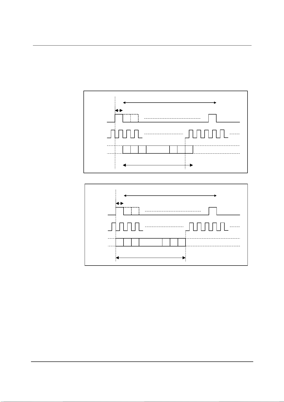
AC97 INTERFACE TIMING
CLOCK SPECIFICATI ONS
BITCLK
SYNC
t
CLK_HIGH
t
CLK_PERIOD
t
SYNC_HIGH
t
SYNC_PERIOD
t
CLK_LOW
t
SYNC_LOW
Figure 1 Clock Specifications (50pF External Load)
Test Conditions
DBVDD = 3.3V, DCVDD = 3.3V, DGND1 = DGND2 = 0V, TA = -25°C to +85°C, unless otherwise
stated.
PARAMETER SYMBOL MIN TYP MAX UNIT
BITCLK frequency
BITCLK period
BITCLK output jitter
BITCLK high pulse width (Note 1)
BITCLK low pulse width (Note 1)
SYNC frequency
SYNC period
SYNC high pulse width
SYNC low pulse width
12.288 MHz
t
CLK_PERIOD
81.4 ns
750 ps
t
36 40.7 45 ns
CLK_HIGH
t
36 40.7 45 ns
CLK_LOW
48 kHz
t
SYNC_PERIOD
t
SYNC_HIGH
t
SYNC_LOW
20.8 µs
1.3 µs
19.5 µs
Note:
1. Worst case duty cycle restricted to 45/55
w
PP, Rev 3.2, October 2008
11
Page 12

WM9714L Pre-Production
DATA SETUP AND HOLD
Figure 2 Data Setup and Hold (50pF External Load)
Note:
Setup and hold times for SDATAIN are with respect to the AC’97 controller, not the
WM9713L.
Test Conditions
DBVDD = 3.3V, DCVDD = 3.3V, DGND1 = DGND2 = 0V, TA = -25°C to +85°C, unless otherwise
stated.
PARAMETER SYMBOL MIN TYP MAX UNIT
Setup to falling edge of BITCLK
Hold from falling edge of BITCLK
Output valid delay from rising edge of
BITCLK
t
10 ns
SETUP
t
10 ns
HOLD
t
15 ns
CO
w
PP, Rev 3.2, October 2008
12
Page 13

Pre-Production WM9714L
SIGNAL RISE AND FALL TIMES
t
BITCLK
SYNC
SDATAIN
SDATAOUT
t
t
rise
rise
t
rise
rise
CLK
SYNC
DIN
DOUT
t
fall
CLK
t
fall
SYNC
t
fall
DIN
t
fall
DOUT
Figure 3 Signal Rise and Fall Times (50pF External Load)
Test Conditions
DBVDD = 3.3V, DCVDD = 3.3V, DGND1 = DGND2 = 0V, TA = -25°C to +85°C, unless otherwise
stated.
PARAMETER SYMBOL MIN TYP MAX UNIT
BITCLK rise time
BITCLK fall time
SYNC rise time
SYNC fall time
SDATAIN rise time
SDATAIN fall time
SDATAOUT rise time
SDATAOUT fall time
trise
2 6 ns
CLK
tfall
2 6 ns
CLK
trise
6 ns
SYNC
tfall
6 ns
SYNC
trise
2 6 ns
DIN
tfall
2 6 ns
DIN
trise
6 ns
DOUT
tfall
6 ns
DOUT
AC-LINK POWERDOWN
SLOT 1 SLOT 2
SYNC
BITCLK
w
SDATAOUT
SDATAIN
WRITE
TO 0X20
DATA PR4
t
S2_PDOWN
DON'T
CARE
Figure 4 AC-Link Powerdown Timing
AC-Link powerdown occurs when PR4 (register 26h, bit 12) is set (see “Power Management”
section).
PARAMETER SYMBOL MIN TYP MAX UNIT
End of Slot 2 to BITCLK and SDATAIN
t
S2_PDOWN
1.0 µs
low
PP, Rev 3.2, October 2008
13
Page 14

WM9714L Pre-Production
COLD RESET (ASYNCHRONOUS, RESETS REGISTER SETTINGS)
Figure 5 Cold Reset Timing
Note:
For correct operation SDATAOUT and SYNC must be held LOW for entire RESETB active
low period otherwise the device may enter test mode. See AC'97 specification or Wolfson
applications note W AN104 for more details.
PARAMETER SYMBOL MIN TYP MAX UNIT
RESETB active low pulse width t
WARM RESET (ASYNC HRONOUS, PRESERVES REGISTER SETTINGS)
1.0 µs
RST_LOW
Figure 6 Warm Reset Timing
PARAMETER SYMBOL MIN TYP MAX UNIT
SYNC active high pulse width
SYNC inactive to BITCLK startup
delay
t
SYNC_HIGH
t
1.3 µs
162.4 ns
RST2CLK
w
PP, Rev 3.2, October 2008
14
Page 15

Pre-Production WM9714L
PCM AUDIO INTERFACE TIMING – SLAVE MODE
Figure 7 Digital Audio Data Timing – Slave Mode
Test Conditions
DBVDD = 3.3V, DCVDD = 3.3V, DGND1 = DGND2 = 0V, TA = -25°C to +85°C, unless otherwise stated.
PARAMETER SYMBOL MIN TYP MAX UNIT
Audio Data Input Timing Information
PCMCLK cycle time
PCMCLK pulse width high
PCMCLK pulse width low
PCMFS set-up time to PCMCLK rising edge
PCMFS hold time from PCMCLK rising edge
PCMDAC set-up time from PCMCLK rising edge
PCMDAC hold time from PCMCLK rising edge
PCMADC propagation delay from PCMCLK falling edge
Note:
1. PCMCLK period should always be greater than or equal to Voice CLK period.
t
50 ns
PCMY
t
20 ns
PCMH
t
20 ns
PCML
t
10 ns
FSSU
t
10 ns
FSH
t
10 ns
DS
t
10 ns
DH
t
10 ns
DD
w
PP, Rev 3.2, October 2008
15
Page 16

WM9714L Pre-Production
PCM AUDIO INTERFACE TIMING – MASTER MODE
Figure 8 Digital Audio Data Timing – Master Mode (see Control Interface)
Test Conditions
DBVDD = 3.3V, DCVDD = 3.3V, DGND1 = DGND2 = 0V, TA = -25°C to +85°C, unless otherwise stated.
PARAMETER SYMBOL MIN TYP MAX UNIT
Audio Data Input Timing Information
PCMFS propagation delay from PCMCLK falling edge
PCMADC propagation delay from PCMCLK falling edge
PCMDAC setup time to PCMCLK rising edge
PCMDAC hold time from PCMCLK rising edge
t
10 ns
DL
t
10 ns
DDA
t
10 ns
DST
t
10 ns
DHT
w
PP, Rev 3.2, October 2008
16
Page 17

Pre-Production WM9714L
DEVICE DESCRIPTION
INTRODUCTION
The WM9714L is a largely pin compatible upgrade to WM9712, with a PCM voice codec added. This
codec is interfaced via a PCM type audio interface which makes use of GPIO pins for connection.
It is designed to meet the mixed-signal requirements of portable and wireless smartphone systems. It
includes audio recording and playback, battery monitoring, auxiliary ADC and GPIO functions, all
controlled through a single 5-wire AC-Link interface. Additionally, PCM voice codec functions are
supported through provision of an additional voice DAC and a PCM audio serial interface.
A PLL is included to allow unrelated reference clocks to be used for generation of the AC link system
clock. Typically 13MHz or 2.048MHz clock sources might be used as a reference.
SOFTWARE SUPPORT
The basic audio features of the WM9714L are software compatible with standard AC’97 device
drivers. However, to better support additional functions, Wolfson Microelectronics supplies custom
device drivers for selected CPUs and operating systems. Please contact your local Wolfson Sales
Office for more information.
AC’97 COMPATIBILITY
The WM9714L uses an AC’97 interface to communicate with a microprocessor or controller. The
audio and GPIO functions are largely compliant with AC’97 Revision 2.2. The following differences
from the AC’97 standard are noted:
• Pinout: The function of some pins has been changed to support device specific
features. The PHONE and PCBEEP pins have been moved to different locations
on the device package.
• Package: The default package for the WM9714L is a 7×7mm leadless QFN
package.
• Audio mixing: The WM9714L handles all the audio functions of a smartphone,
including audio playback, voice recording, phone calls, phone call recording, ring
tones, as well as simultaneous use of these features. The AC’97 mixer architecture
does not fully support this. The WM9714L therefore uses a modified AC’97 mixer
architecture with three separate mixers.
• Tone Control, Bass Boost and 3D Enhancement: These functions are implemented
in the digital domain and therefore affect only signals being played through the
audio DACs, not all output signals as stipulated in AC’97.
Some other functions are additional to AC’97:
• On-chip BTL loudspeaker driver for mono or stereo speakers
• On-chip BTL driver for ear speaker (phone receiver)
• Auxiliary mono DAC for ring tones, system alerts etc.
• Auxiliary ADC Inputs
• 2 Analogue Comparators for Battery Alarm
• Programmable Filter Characteristics for Tone Control and 3D Enhancement
• PCM interface to additional Voice DAC and existing audio ADCs
• PLL to create AC’97 system clock from unrelated reference clock input
PCM CODEC
w
The PCM voice codec functions typically required by mobile telephony devices are provided by an
extra voice DAC on the WM9714L, which is interfaced via a standard PCM type data interface, which
is constructed through optional use of 4 of the GPIO pins on WM9714L. The audio output data from
one or both of the audio ADCs can also be output over this PCM interface, allowing a full voice codec
function to be implemented. This PCM interface supports sample rates from 8 to 48ks/s using the
standard AC’97 master clock.
PP, Rev 3.2, October 2008
17
Page 18

WM9714L Pre-Production
AUDIO PATHS OVERVIEW
WM9713 Analogue
Note: all PGAs and summers are inverting
18 Bit DACL
slot 3
18 Bit ADC
Variable Slot
5C:1-0 (ASS)
5C:3 (HPF)
5C:4 (ADCO)
ALC:5Ch/60h/62h
18 Bit DAC R
slot 3
00000 = +12dB
11111 = -34.5dB
16 Bit PCM
VXDAC
00000 = +12dB
11111 = -34.5dB
12 Bit Resistor
string DAC
2Eh/64h
0Ch:12-8
0Ch:4-0
Sent to Both
PCM Link
AC'97 Link
MONOMIX
HPMIXL
HPMIXR
DACR
DACL
LINER
LINEL
PCBEEP
MONOIN
MIC2
MICA
RECMUXR
RECMUXL
AUXDAC
VXDAC
DACL
LINEL
MONOIN
PCBEEP
MICA
MICB
RECMUXL
RECMUXR
AUXDAC
VXDAC
DACR
DACL
LINER
LINEL
PCBEEP
MONOIN
MICB
MICA
RECMUXR
RECMUXL
AUXDAC
VXDAC
DACL
DACR
LINEL
LINER
PCBEEP
MICA
MICB
RECMUXL
RECMUXR
AUXDAC
VXDAC
DACR
DACL
LINER
LINEL
PCBEEP
MONOIN
MICB
MICA
RECMUXR
RECMUXL
AUXDAC
VXDAC
DACR
DACL
LINER
LINEL
PCBEEP
MONOIN
MICB
MICA
RECMUXR
RECMUXL
AUXDAC
VXDAC
DACR
LINER
MONOIN
PCBEEP
MICA
MICB
RECMUXL
RECMUXR
AUXDAC
VXDAC
DACR
DACL
LINER
LINEL
PCBEEP
MONOIN
MICB
MICA
RECMUXR
RECMUXL
AUXDAC
VXDAC
LINEL
LINER
DACL
DACR
MONOIN
PCBEEP
AUXDAC
VXDAC
6dB -> -15dB
6dB -> -15dB
6dB -> -15dB
6dB -> -15dB
6dB -> -15dB
6dB -> -15dB
6dB -> -15dB
6dB -> -15dB
6dB -> -15dB
6dB -> -15dB
6dB -> -15dB
6dB -> -15dB
6dB -> -15dB
6dB -> -15dB
6dB -> -15dB
6dB -> -15dB
6dB -> -15dB
6dB -> -15dB
6dB -> -15dB
6dB -> -15dB
0
C
h
:
1
0
A
5
h
:
1
5
0
8
h
:
Headphone
1
5
1
6
h
Mixer L
:
1
5
-
1
2
1
0
h
:
4
-
0
10h:4-0
1
1
-
5
1
:
h
4
1
1
1
-
5
1
:
h
4
2
1
1
-
5
1
:
2
h
1
A
-
1
5
1
:
h
8
1
0
C
h
:
1
0
C
3
h
:
1
0
3
A
h
:
MONO
1
3
0
A
Mixer
h
:
1
3
1
6
h
7
:
4
0dB / 20dB
10h:7+5
5
+
6
:
h
0dB / 20dB
0
1
8
-
0
1
:
h
4
1
8
0dB / 20dB
-
0
1
:
h
4
4
-
1
7
:
h
0dB / 20dB
4
A
-
1
7
:
h
8
1
0
C
h
:
1
0
5
A
h
:
1
5
0
8
h
:
Headphone
1
5
1
6
h
Mixer R
:
1
5
-
1
2
1
0
h
:
4
-
0
10h:4-0
1
1
-
5
1
:
h
4
1
1
1
-
5
1
:
h
4
2
1
1
-
5
1
:
2
h
1
A
-
1
5
1
:
h
8
1
0
A
h
:
1
4
0
A
h
1
Speaker
4
0
C
Mixer
h
:
1
4
0
C
h
:
1
4
08h:14
8
-
1
1
:
h
6
1
8
-
1
1
:
h
A
1
8
-
1
1
:
h
8
1
SPKMIX
MONOMIX
HPMIXL
HPMIXR
SPKMIX
MONOMIX
HPMIXL
HPMIXR
SPKMIX
MONOMIX
HPMIXL
HPMIXR
SPKMIX
INV1
INV2
1Eh:15-13
INV1
INV1
INV1
04h:12-8
00000 = 0dB
11111 = -46.5dB
HPMIXL
1Ch:7-6
Vmid
HPMIXL
SPKMIX
INV1
1Ch:13-11
Vmid
MONOMIX
INV1
1Ch:15-14
Vmid
INV2
INV1
Vmid
INV2
Vmid
INV2
HPMIXR
1Ch:5-4
Vmid
HPMIXR
SPKMIX
INV2
1Ch:10-8
Vmid
INV2
04h:15 (MUTE)
02h:12-8
00000 = 0dB
11111 = -46.5dB
02h:15 (MUTE)
08h:4-0
00000 = 0dB
11111 = -46.5dB
08h:7 (MUTE)
11111 = -46.5dB
1Ch:3-2
11111 = -46.5dB
1Ch:1-0
04h:4-0
00000 = 0dB
11111 = -46.5dB
04h:7 (MUTE)
02h:4-0
00000 = 0dB
11111 = -46.5dB
02h:7 (MUTE)
Zero-cross
detect
04h:14 (ZC)
Zero-cross
detect
02h:14 (ZC)
Zero-cross
detect
08h:6 (ZC)
06h:4-0
00000 = 0dB
06h:7 (MUTE)
06h:12-8
00000 = 0dB
06h:15 (MUTE)
Zero-cross
detect
04h:6 (ZC)
Zero-cross
detect
02h:6 (ZC)
Zero-cross
detect
06h:6 (ZC)
Zero-cross
detect
06h:14 (ZC)
HPL
SPKL
MONO
OUT3
OUT4
HPR
SPKR
LINEL
MONOIN
PCBEEP
LINER
MIC1
MIC2A
MIC2B
MICCM
40h:7
(Loopback)
ADC Left
0Ah:12-8
00000 = +12dB
11111 = -34.5dB
08h:12-8
00000 = +12dB
11111 = -34.5dB
Tone and 3D
1Eh / 20h /
40h:13 (3DE)
AC'97 Link
LINER
LINEL
MICB
MICA
PCBEEP
MONOIN
PCM Link
0Eh:12-8
00000 = +12dB
11111 = -34.5dB
LINER
LINEL
MICB
MICA
PCBEEP
MONOIN
12h:14 (GRL=0)
12h:11:8
0000 = 0db
1111 = +22.5dB
12h:14 (GRL=1)
12h:13-8
14h:6
11111 = +30dB
0 = 0dB
00000 = -17.25dB
1 = 20dB
14h:5-3
40h:7
LINER
LINEL
MICB
MICA
MONOIN
Vmid
22h:
22h:11-10
13-12
00 = +12dB
Vmid
11 = +30dB
(Loopback)
PCBEEP
AC'97 Link
ADC Right
0Ah:4-0
00000 = +12dB
11111 = -34.5dB
Tone and 3D
1Eh / 20h /
40h:13 (3DE)
AC'97 Link
Vmid
22h:9-8
00 = +12dB
11 = +30dB
LINER
LINEL
MICB
MICA
PCBEEP
MONOIN
0Eh:4-0
00000 = +12dB
11111 = -34.5dB
MICB
MICA
LINEL
LINER
PCBEEP
MONOIN
PR Bit Code
PR0 - Audio ADCs & record mux
PR1 - Stereo DAC
PR2 - Input PGAs & mixers
PR3 - Refs, input PGAs, mixers & output PGAs
PR6 - Output PGAs
Note: PR bits are active low - i.e. 0 = "ON"; 1 = "OFF"
=> Enable when { (PR0 || PR2) && PR3 } are low
Figure 9 Audio Paths Overview
w
12h:6 (GRR=0)
12h:3:0
0000 = 0db
1111 = +22.5dB
12h:6 (GRR=1)
12h:5-0
11111 = +30dB
00000 = -17.25dB
14h:2-0
0 = 0dB
1 = 20dB
MICB
MICA
DACL
LINEL
DACR
LINER
14h:6
18 Bit ADC
Variable Slot
5C:1-0 (ASS)
5C:3 (HPF)
5C:4 (ADCO)
ALC:5Ch/60h/62h
Sent to Both
PCM Link
AC'97 Link
MONOIN
VXDAC
PCBEEP
AUXDAC
RECMUXL
RECMUXR
1Eh:12-10
INV1
HPMIXL
SPKMIX
HPMIXR
MONOMIX
INV2
VMICBI AS
AGNDAVDD CAP
VREF
PP, Rev 3.2, October 2008
18
Page 19

Pre-Production WM9714L
CLOCK GENERATION
WM9714L supports clocking from 2 separate sources, which can be selected via the AC’97 interface:
• External clock input MCLKA
• External clock input MCLKB
The source clock is divided to appropriate frequencies in order to run the AC’97 interface, PCM
interface, voice DAC and Hi-fi DSP by means of a programmable divider block. Clock rates may be
changed during operation via the AC’97 link in order to support alternative modes, for example low
power mode when voice data is being transmitted only. A PLL is present to add flexibility in selection
of input clock frequencies, typical choices being 2.048MHz, 4.096MHz or 13MHz.
INITIALISING THE AC’97 LINK
By default, the AC’97 link is disabled and therefore will not be running after power on or a COLD
reset event. Before any register map configuration can begin, it is necessary to start the AC’97 link.
This is achieved by sending a WARM reset to the CODEC as defined in Figure 6.
Default mode on power-up also assumes a clock will be present on MCLKA with the PLL powered
down. After a WARM reset the CODEC will start the AC’97 link using MCLKA as a reference. This
enables data to be clocked via the AC’97 link to define the desired clock divider mode and whether
PLL needs to be activated.
Note: MCLKA can be any available frequency.
When muxing between MCLKA and MCLKB both clocks must be active for at least two clock cycles
after the switching event.
CLOCK DIVISION MODES
Figure 10 shows the clocking strategy for WM9714L. Clocking is controlled by CLK_MUX, CLK_SRC
and S[6:0].
• CLKAX2, CLKBX2 – clock doublers on inputs MCLKA and MCLKB.
• CLK_MUX - selects between MCLKA and MCLKB.
• CLK_SRC – selects between external or PLL derived clock reference.
• S[3:0] – sets the voice DAC clock rate and PCM interface clock when in master mode
• S[6:4] - sets the hi-fi clocking rate (division ratio 1 to 8 available).
The registers used to set these switches can be accessed from register address 44h (see Table 3).
If a mode change requires switching from an external clock to a PLL generated clock then it is
recommended to set the clock division ratios required for the PLL clock scheme prior to switching
between clocks. This option is accommodated by means of two sets of registers. S
set the divide ratio of the clock when in PLL mode and S
derived from an external source. If the PLL is selected (CLK_SRC = 0), S[6:0] = S
is defined in register 46h (see Table 4) and is written to using the page address mode. More details
on page address mode for controlling the PLL are found on page 20. Register 46h also contains a
number of separate control bits relating to the PLL’s function. If an external clock is selected
(CLK_SRC = 1) S[6:0] = S
44h and 46h enables pre-programming of the required clock mode before the PLL output is selected.
(division ratio 1 to 16 available).
[6:0]. S
EXT
EXT
[6:0] is used to
PLL
[6:0] is used to divide the clock when it is
EXT
[6:0]. S
PLL
[6:0] is defined in register address 44h. Writing to registers
PLL
[6:0]
w
PP, Rev 3.2, October 2008
19
Page 20

WM9714L Pre-Production
Figure 10 Clocking Architecture for WM9714L
INTERNAL CLOCK FREQUENCIES
The internal clock frequencies are defined as follows (refer to Figure 10):
• AC97 CLK – nominally 24.576MHz, used to generate AC97 BITCLK at 12.288MHz.
• HIFI CLK – for HIFI playback at 48ks/s HIFI CLK = 24.576MHz. See Table 2 for voice only
playback.
• Voice DAC CLK – see Table 2 for sample rate vs clock frequency.
SAMPLE RATE VOICE DAC CLK
FREQUENCY
8ks/s voice and HIFI 2.048MHz 24.576MHz
8ks/s voice only (power save) 2.048MHz 4.096MHz
16ks/s voice and HIFI 4.096MHz 24.576MHz
16ks/s voice only (power save) 4.096MHz 8.192MHz
32ks/s voice and HIFI 8.192MHz 24.576MHz
48ks/s voice and HIFI 12.288MHz 24.576MHz
Table 2 Clock Division Mode Table
HIFI CLK
FREQUENCY
AUXADC
The clock for the AUXADC nominally runs at 768kHz and is derived from BITCLK. The divisor for the
clock generator is set by PENDIV. This enables the AUXADC clock frequency to be set according to
power consumption and conversion rate considerations.
w
PP, Rev 3.2, October 2008
20
Page 21

Pre-Production WM9714L
Clock mode and division ratios are controlled by register 44h as shown in Table 3.
REGISTER
ADDRESS
44h
Table 3 Clock Muxing and Division Control
BIT LABEL DEFAULT DESCRIPTION
14:12 S
11:8 S
7 CLKSRC 1 (ext clk) Selects between PLL clock and External
5:3 PENDIV 000 (div 16) Sets AUXADC clock divisor
2 CLKBX2 0 (Off) Clock doubler for MCLKB
1 CLKAX2 0 (Off) Clock doubler for MCLKA
0 CLKMUX 0 (MCLKA) Selects between MCLKA and MCLKB
[6:4] 000 (div 1) Defines clock division ratio for Hi-fi:
EXT
DSP, ADCs and DACs
000: f
001: f/2
...
111: f/8
[3:0] 0000 (div 1) Defines clock division ratio for PCM
EXT
interface and voice DAC in external clock
mode only:
0000: f
0001: f/2
…
1111: f/16
clock
0: PLL clock
1: external clock
000: f/16
001: f/12
010: f/8
011: f/6
100: f/4
101: f/3
110: f/2
111: f
(N.B. On power-up clock must be present
on MCLKA and must be active for 2 clock
cycles after switching to MCLKB)
0: SYSCLK=MCLKA
1: SYSCLK=MCLKB
w
PP, Rev 3.2, October 2008
21
Page 22

WM9714L Pre-Production
PLL MODE
The PLL operation is controlled by register 46h (see Table 4) and has two modes of operation:
• Integer N
• Fractional N
The PLL has been optimized for nominal input clock (PLL_IN) frequencies in the range 8.192MHz –
19.661MHz (LF=0) and 2.048MHz – 4.9152MHz (LF=1). Through use of a clock divider (div by 2 / 4)
on the input to the PLL frequencies up to 78.6MHz can be accommodated. The input clock divider is
enabled by DIVSEL (0=Off) and the division ratio is set by DIVCTL (0=div2, 1=div4).
Figure 11 PLL Architecture
REGISTER
ADDRESS
46h
Table 4 PLL Clock Control
BIT LABEL DEFAULT DESCRIPTION
15:12 N[3:0] 0000 PLL N Divide Control
11 LF 0 = off PLL Low Frequency Input Control
10 SDM 0 = off PLL SDM Enable Control
9 DIVSEL 0 = off PLL Input Clock Division Control
8 DIVCTL 0 PLL Input Clock Division Value Control
6:4 PGADDR 000 Pager Address
3:0 PGDATA 0000 Pager Data
0000 = Divide by 1
0001 = Divide by 1
0010 = Divide by 2
…
1111 = Divide by 15
Note: must be set between 05h and 0Ch for
integer N mode
1 = Low frequency mode (input clock <
8.192MHz)
0 = Normal mode
1 = Enable SDM (required for fractional N
mode)
0 = Disable SDM
0 = Divide by 1
1 = Divide according to DIVCTL
0 = Divide by 2
1 = Divide by 4
Pager address bits to access programming
of K[21:0] and S
Pager data bits
PLL
[6:0]
w
PP, Rev 3.2, October 2008
22
Page 23

Pre-Production WM9714L
INTEGER N M OD E
The nominal output frequency of the PLL (PLL_OUT) is 98.304MHz which is divided by 4 to achieve
a nominal system clock of 24.576MHz.
The integer division ratio (N) is determined by: F
the range 5 to 12 for integer N operation (0101 = div by 5, 1100 = div by 12). Note that setting LF=1
enables a further division by 4 required for input frequencies in the range 2.048MHz – 4.096MHz.
Integer N mode is selected by setting SDM=0.
PLL_out
/ F
, and is set by N[3:0] and must be in
PLL_IN
FRACTIONAL N MODE
Fractional N mode provides a divide resolution of 1/222 and is set by K[21:0] (register 46h, see
section). The relationship between the required division X, the fractional division K[21:0] and the
integer division N[3:0] is:
()
NXK −=222
where 0 < (X – N) < 1 and K is rounded to the nearest whole number.
For example, if the PLL_IN clock is 13MHz and the desired PLL_OUT clock is 98.304MHz then the
desired division, X, is 7.5618. So N[3:0] will be 7h and K[21:0] will be 23F488h to produce the desired
98.304MHz clock (see Table 5).
INPUT CLOCK (PLL_IN) DESIRED
PLL
OUTPUT
(PLL_OUT)
2.048MHz 98.304MHz
4.096MHz 98.304MHz
12.288MHz 98.304MHz
13MHz 98.304MHz
27MHz (13.5MHz)** 98.304MHz
*Divide by 4 enabled in PLL feedback path for low frequency inputs. (LF = 1)
**Divide by 2 enabled at PLL input for frequencies > 14.4MHz > 38MHz (DIVSEL = 1, DIVCTL = 0)
Table 5 PLL Modes of Operation
DIVISION
REQUIRED
(X)
48 0 12x4*
24 0 6x4*
8 0 8
7.5618 0.5618 7
7.2818 0.2818 7
FRACTIONAL
DIVISION (K)
INTEGER
DIVISION (N)
w
PP, Rev 3.2, October 2008
23
Page 24

WM9714L Pre-Production
PLL REGISTER PAGE ADDRESS MAPPING
The clock division control bits S
register 46h using a sub-page address system. The 3 bit pager address allows 8 blocks of 4 bit data
words to be accessed whilst the register address is set to 46h. This means that when register
address 46h is selected a further 7 cycles of programming are required to set all of the page data
bits. Control bit allocation for these page addresses is described in Table 6.
PAGE
ADDRESS
111 31:28 S
110 27:24 S
100 19:16 0h
011 15:12 0h
010 11:8 0h
001 7:4 0h
000 3:0
Table 6 Pager Control Bit Allocation
Powerdown for the PLL and internal clocks is via registers 26h and 3Ch (see Table 7).
REGISTER
ADDRESS
26h 13 PR5 1 (Off) Internal Clock Disable Control
3Ch 9 PLL 1 (Off) PLL Disable Control
N.B. both PR5 and PLL must be asserted low before PLL is enabled
Table 7 PLL Powerdown Control
BIT LABEL DEFAULT DESCRIPTION
23:22 Reserved 0h Reserved bits 101
21:20 0h
BIT LABEL DEFAULT DESCRIPTION
[6:0] and the PLL fractional N division bits are accessed through
PLL
[6:4] 0h
PLL
[3:0] 0h
PLL
K[21:0]
0h
Clock division control bus SPLL[6:0]. Clock
divider reads this control word if PLL is
enabled. Bits [6:4] and [3:0] have the same
functionality as 44h [14:12] and [11:8]
respectively
Sigma Delta Modulator control word for
fractional N division. Division resolution is
2
1/22
1 = Disabled
0 = Enabled
1 = Disabled
0 = Enabled
w
PP, Rev 3.2, October 2008
24
Page 25

Pre-Production WM9714L
DIGITAL INTERFACES
The WM9714L has two interfaces, a data and control AC’97 interface and a data only PCM interface.
The AC’97 interface is available through dedicated pins (SDATAOUT, SDATAIN, SYNC, BITCLK and
RESETB) and is the sole control interface with access to all data streams on the device except for
the Voice DAC. The PCM interface is available through the GPIO pins (PCMCLK, PCMFS, PCMDAC
and PCMADC) and provides access to the Voice DAC. It can also transmit the data from the Stereo
ADC. This can be useful, for example, to allow both sides of a phone conversation to be recorded by
mixing the transmit and receive paths on one of the ADC channels and transmitting it over the PCM
interface.
AC97 INTERFACE
INTERFACE PROTO COL
The WM9714L uses an AC’97 interface for both data transfer and control. The AC-Link has 5 wires:
• SDATAIN (pin 8) carries data from the WM9714L to the controller
• SDATAOUT (pin 5) carries data from the controller to the W M9714L
• BITCLK (pin 6) is a clock, derived from either MCLKA or MCLKB inputs and
supplied to the controller.
• SYNC is a synchronization signal generated by the controller and passed to the
WM9714L
• RESETB resets the WM9714L to its default state
Figure 12 AC-Link Interface (typical case with BITCLK generated by the AC97 codec)
The SDATAIN and SDATAOUT signals each carry 13 time-division multiplexed data streams (slots 0
to 12). A complete sequence of slots 0 to 12 is referred to as an AC-Link frame, and contains a total
of 256 bits. The frame rate is 48kHz. This makes it possible to simultaneously transmit and receive
multiple data streams (e.g. audio, AUXADC, control) at sample rates up to 48kHz.
Detailed information can be found in the AC’97 (Revision 2.2) specification, which can be obtained at
www.intel.com/design/chipsets/audio/
Note:
SDATAOUT and SYNC must be held low when RESETB is applied. These signals must be held low
for the entire duration of the RESETB pulse and especially during the low-to-high transition of
RESETB. If SDATAOUT or SYNC is high during reset, the W M9714L may enter test modes.
Information relating to this operation is available in the AC'97 specification or in Wolfson applications
note WAN-0104 available at www.wolfsonmirco.com.
w
PP, Rev 3.2, October 2008
25
Page 26

WM9714L Pre-Production
PCM INTERFACE
OPERATION
WM9714L can implement a PCM voice codec function using the dedicated VXDAC and either one or
both of the existing hi-fi ADC’s. In PCM codec mode, VXDAC input and ADC output are interfaced
via a PCM style port via GPIO pins.
This interface can support one ADC channel, or stereo/dual ADC channels if required, (two channels
of data are sent per PCM frame as back to back words).
In voice only mode, the AC link is used only for control information, not audio data. Therefore it will
generally be shut down (PR4=1), except when control data must be sent.
The PCM interface makes use of 4 of the GPIO interface pins, for clock, frame, and data in/out. If the
PCM codec function is not enabled then the GPIO pins may be used for other functions.
INTERFACE PROTO COL
The WM9714L PCM audio interface is used for the input of data to the Voice DAC and the output of
data from the Stereo ADC. When enabled, the PCM audio interface uses four GPIO pins:
• GPIO1/PCMCLK: Bit clock
• GPIO3/PCMFS: Frame Sync
• GPIO4/PCMDAC: Voice DAC data input
• GPIO5/PCMADC: Stereo ADC data output
Depending on the mode of operation (see “PCM Interface Modes”), at least one of these four pins
must be set up as an output by writing to register 4Ch (see Table 57). When not enabled the GPIOs
may be used for other functions on the WM9714L.
PCM INTERFACE MODES
The WM9714L PCM audio interface may be configured in one of four modes:
• Disabled Mode: The WM9714L disables and tri-states all PCM interface pins. Any
clock input is ignored and ADC/DAC data is not transferred.
• Slave Mode: The WM9714L accepts PCMCLK and PCMFS as inputs from an
external source.
• Master Mode: The WM9714L generates PCMCLK and PCMFS as outputs.
• Partial Master Mode: The WM9714L generates PCMCLK as an output, and
accepts PCMFS as an external input.
PCM AUDIO DATA FORMATS
Four different audio data formats are supported:
• DSP mode
• Left justified
• Right justified
2
• I
S
All four of these modes are MSB first. They are described below. Refer to the Electrical
Characteristic section for timing information.
Note:
PCMCLK and PCMFS must be synchronized with the BITCLK from the AC’97 interface.
w
PP, Rev 3.2, October 2008
26
Page 27
Pre-Production WM9714L
The PCM Interface may be configured for Mono mode, where only one channel of ADC data is
output. In this mode the interface should be configured for DSP mode. A short or long frame sync is
supported and the MSB is available on either the 1st (mode B) or 2nd (mode A) rising edge of
VXCLK.
Note that when operating in stereo mode the mono Voice DAC always uses the left channel data as
its input.
1/fs
1 PCMCLK
PCMFS
PCMCLK
PCMADC/
PCMDAC
Input Word Length (WL)
Figure 13 PCM Interface Mono Mode (mode A, FSP=0)
1 PCMCLK
PCMFS
PCMCLK
PCMADC/
PCMDAC
n-2 n-1
n-2 n-1
LSBMSB
Input Word Length (WL)
Figure 14 PCM Interface Mono Mode (mode B, FSP=1)
n321
LSBMSB
1/fs
n321
w
PP, Rev 3.2, October 2008
27
Page 28

WM9714L Pre-Production
In DSP mode, the left channel MSB is available on either the 1st (mode B) or 2nd (mode A) rising
edge of PCMCLK (selectable by FSP) following a rising edge of PCMFS. Right channel data
immediately follows left channel data. Depending on word length, PCMCLK frequency and sample
rate, there may be unused PCMCLK cycles between the LSB of the right channel data and the next
sample.
1/fs
1 BCLK / VXCLK
PCMFS
PCMCLK
RIGHT CHANNEL
PCMADC/
PCMDAC
LEFT CHANNEL
n-2 n-1
Input Word Length ( WL)
n321
LSBMSB
Figure 7 DSP Mode Audio Interface (mode A, FSP=0)
1/fs
1 BCLK / VXCLK
PCMFS
PCMCLK
RIGHT CHANNEL
PCMADC/
PCMDAC
LEFT CHANNEL
n-2 n-1
Input Word Length (W L)
n321
LSBMSB
Figure 15 DSP Mode Audio Interface (mode B, FSP=1)
n-2 n-1
n-2 n-1
n321
n321
w
PP, Rev 3.2, October 2008
28
Page 29

Pre-Production WM9714L
In Left Justified mode, the MSB is available on the first rising edge of PCMCLK following a PCMFS
transition. The other bits up to the LSB are then transmitted in order. Depending on word length,
PCMCLK frequency and sample rate, there may be unused PCMCLK cycles before each PCMFS
transition.
1/fs
LEFT CHANNEL RIGHT CHANNEL
PCMFS
PCMCLK
PCMADC/
PCMDAC
n-2 n-1
n321
LSBMSB
n-2 n-1
n321
LSBMSB
Figure 16 Left Justified Audio Interface (assuming n-bit word length)
In Right Justified mode, the LSB is available on the last rising edge of PCMCLK before a PCMFS
transition. All other bits are transmitted before (MSB first). Depending on word length, PCMCLK
frequency and sample rate, there may be unused PCMCLK cycles after each PCMFS transition.
1/fs
LEFT CHANNEL RIGHT CHANNEL
PCMFS
PCMCLK
PCMADC /
PCMDAC
n-2 n-1
n321
LSBMSB
n-2 n-1
n321
LSBMSB
Figure 17 Right Justified Audio Interface (assuming n-bit word length)
2
In I
S mode, the MSB is available on the second rising edge of PCMCLK following a PCMFS
transition. The other bits up to the LSB are then transmitted in order. Depending on word length,
PCMCLK frequency and sample rate, there may be unused PCMCLK cycles between the LSB of one
sample and the MSB of the next.
w
1/fs
LEFT CHANNEL RIGHT CHANNEL
PCMFS
PCMCLK
PCMADC/
PCMDAC
MSB
1 BCLK
n-2 n-1
n321
LSB
1 BCLK
MSB
Figure 18 I2S Justified Audio Interface (assuming n-bit word length)
n321
n-2 n-1
LSB
PP, Rev 3.2, October 2008
29
Page 30

WM9714L Pre-Production
CONTROL
The register bits controlling PCM audio format, word length and operating modes are summarised
below. CTRL must be set to override the normal use of the PCM interface pins as GPIOs, MODE
must be set to specify master/slave modes.
REGISTER
ADDRESS
36h
PCM
Control
Table 8 PCM Codec Control
BIT LABEL DEFAULT DESCRIPTION
15 CTRL 0 GPIO Pin Configuration Control
0 = GPIO pins as GPIOs
1 = GPIO pins configured as PCM interface
and controlled by this register
14:13 MODE 10 PCM Interface Mode Control
00 = PCM interface disabled [PCMCLK tri-
stated, PCMFS tri-stated]
01 = PCM interface in slave mode [PCMCLK
as input, PCMFS as input]
10 = PCM interface in master mode [PCMCLK
as output, PCMFS as output]
11 = PCM interface in partial master mode
[PCMCLK as output, PCMFS as input]
11:9 DIV 010 PCMCLK Rate Control
000 = Voice DAC clock
001 = Voice DAC clock / 2
010 = Voice DAC clock / 4
011 = Voice DAC clock / 8
100 = Voice DAC clock / 16
All other values are reserved
8 VDACOS
R
7 CP 0 PCMCLK Polarity Cont rol
5:4 SEL 10 PCM ADC Output Channel Control
3:2 WL 00 PCM Data Word Length Control
1:0 FMT 11 PCM Data Format Control
1 Voice DAC Oversampling Rate Control
0: 128 x fs
1: 64 x fs
0 = Normal
1 = Inverted
FMT = 00, 01 or 10 FMT = 11 6 FSP 0
PCMFS Pola ri ty
Control
0 = Normal
1 = Inverted
00 = Normal stereo
01 = Reverse stereo
10 = Output left ADC data only
11 = Output right ADC data only
00 = 16-bit
01 = 20-bit
10 = 24-bit
11 = 32-bit (not supported when FMT=00)
00 = Right justified
01 = Left justified
2
10 = I
S
11 = DSP mode
DSP Mode Control
0 = DSP Mode A
1 = DSP Mode B
w
Note: Right justified does not support 32-bit data.
PP, Rev 3.2, October 2008
30
Page 31

Pre-Production WM9714L
AUDIO ADCS
STEREO ADC
The WM9714L has a stereo sigma-delta ADC to digitize audio signals. The ADC achieves high
quality audio recording at low power consumption. The ADC sample rate can be controlled by writing
to a control register (see “Variable Rate Audio”). It is independent of the DAC sample rate.
To save power, the left and right ADCs can be separately switched off using the Powerdown bits
ADCL and ADCR (register 3Ch, bits 5:4), whereas PR0 disables both ADCs (see “Power
Management” section). If only one ADC is running, the same ADC data appears on both the left and
right AC-Link slots.
The output from the ADC can be sent over either the AC link as usual, or output via the PCM
interface which may be configured on the GPIO pins.
HIGH PASS FIL TE R
The WM9714L audio ADC incorporates a digital high pass filter that eliminates any DC bias from the
ADC output data. The filter is enabled by default. For DC measurements, it can be disabled by
writing a ‘1’ to the HPF bit (register 5Ch, bit 3).
This high pass filter corner frequency can be selected to have different values in WM9714L, to suit
applications such as voice where a higher cutoff frequency is required.
REGISTER
ADDRESS
5Ch 3 HPF 0 ADC HPF Disable Control
5Ah 5:4 HPMODE 00 HPF Cut-Off Control
Note: the filter corner frequency is proportional to the sample rate.
Table 9 Controlling the ADC Highpass Filter
BIT LABEL DEFAULT DESCRIPTION
0 = HPF enabled (for audio)
1 = HPF disabled (for DC measurements)
00 = 7Hz @ fs=48kHz
01 = 82Hz @ fs=16kHz
10 = 82Hz @ fs=8kHz
11 = 170Hz @ fs=8kHz
w
ADC SLOT MAPPING
By default, the output of the left audio ADC appears on slot 3 of the SDATAIN signal (pin 8), and the
right ADC data appears on slot 4. However, the ADC output data can also be sent to other slots, by
setting the ASS (ADC slot select) control bits as shown below.
REGISTER
ADDRESS
5Ch
Additional
Functions
(2)
Table 10 ADC Slot Mapping
BIT LABEL DEFAULT DESCRIPTION
1:0 ASS 00
ADC Data Slot Mapping Control
Left Da ta Right Data
00 = Slot 3 Slot 4
01 = Slot 7 Slot 8
10 = Slot 6 Slot 9
11 = Slot 10 Slot 11
PP, Rev 3.2, October 2008
31
Page 32

WM9714L Pre-Production
RECORD SELECTOR
The record selector determines which input signals are routed into the audio ADC. The left and right
channels can be selected independently. This is useful for recording a phone call: one channel can
be used for the RX signal and the other for the TX signal, so that both sides of the conversation are
digitized.
REGISTER
ADDRESS
14h
Record
Routing /
Mux Select
Table 11 Audio Record Selector
BIT LABEL DEFAULT DESCRIPTION
6 RECBST 0 ADC Record Boost Control
1 = +20dB
0 = 0dB
Note: RECBST gain is in addition to the
microphone pre-amps (MPABST and
MPBBST bits) and record gain (GRL and
GRR / GRL bits).
5:3 RECSL 000 Left Record Mux Source Control
000 = MICA (pre-PGA)
001 = MICB (pre-PGA)
010 = LINEL (pre-PGA)
011 = MONOIN (pre-PGA)
100 = HPMIXL
101 = SPKMIC
110 = MONOMIX
111 = Reserved
2:0 RECSR 000 Right Record Mux Source Control
000 = MICA (pre-PGA)
001 = MICB (pre-PGA)
010 = LINEL (pre-PGA)
011 = MONOIN (pre-PGA)
100 = HPMIXL
101 = SPKMIC
110 = MONOMIX
111 = Reserved
w
PP, Rev 3.2, October 2008
32
Page 33

Pre-Production WM9714L
RECORD GAIN
The amplitude of the signal that enters the audio ADC is controlled by the Record PGA
(Programmable Gain Amplifier). The PGA gain can be programmed either by writing to the Record
Gain register, or by the Automatic Level Control (ALC) circuit (see next section). W hen the ALC is
enabled, any writes to the Record Gain register have no effect.
Two different gain ranges can be implemented: the standard gain range defined in the AC’97
standard, or an extended gain range with smaller gain steps. The ALC circuit always uses the
extended gain range, as this has been found to result in better sound quality.
REGISTER
ADDRESS
12h
Record Gain
Table 12 Record Gain Register
BIT LABEL DEFAULT DESCRIPTION
15 RMU 1 Audio ADC Input Mute Control
1 = Mute
0 = No mute
Note: This control applies to both channels
14 GRL 0 Left ADC PGA Gain Range Control
1 = Extended
0 = Standard
13:8 RECVOLL 000000
7 ZC 0 ADC PGA Zero Cross Control
6 GRR 0 Right ADC PGA Gain Range Control
5:0 RECVOLR 000000
Left ADC Recording Volume Control
Standard (GRL=0) Extended (GRL=1)
XX0000: 0dB
XX0001: +1.5dB
… (1.5dB steps)
XX1111: +22.5dB
1 = Zero cross enabled (volume changes
when signal is zero or after time-out)
0 = Zero cross disabled (volume changes
immediately)
1 = Extended
0 = Standard
Right ADC Recording Volume Control
Standard (GRR=0) Extended (GRR=1)
XX0000: 0dB
XX0001: +1.5dB
… (1.5dB steps)
XX1111: +22.5dB
000000: -17.25dB
000001: -16.5dB
… (0.75dB steps)
111111: +30dB
000000: -17.25dB
000001: -16.5dB
… (0.75dB steps)
111111: +30dB
w
The output of the Record PGA can also be mixed into the phone and/or headphone outputs (see
“Audio Mixers”). This makes it possible to use the ALC function for the microphone signal in a
smartphone application.
PP, Rev 3.2, October 2008
33
Page 34

WM9714L Pre-Production
REGISTER
ADDRESS
14h
Record
Routing
Table 13 Record PGA Routing Control
BIT LABEL DEFAULT DESCRIPTION
15:14 R2H 11 (mute) Record Mux to Headphone Mixer Path
13:11 R2HVOL 010 (0dB) Record Mux to Headphone Mixer Path
10:9 R2M 11 (mute) Record Mux to Mono Mixer Path Control
8 R2MBST 0 (OFF) Record Mux to Headphone Mixer Boost
Control
00 = stereo
01 = left ADC only
10 = right ADC only
11=mute left and right
Volume Control
000 = +6dB
… (+3dB steps)
111 = -15dB
00 = stereo
01 = left record mux only
10 = right record mux only
11 = mute left and right
Control
1 = +20dB
0 = 0dB
w
PP, Rev 3.2, October 2008
34
Page 35

Pre-Production WM9714L
AUTOMATIC LEVEL CONTROL
The WM9714L has an automatic level control that aims to keep a constant recording volume
irrespective of the input signal level. This is achieved by continuously adjusting the PGA gain so that
the signal level at the ADC input remains constant. A digital peak detector monitors the ADC output
and changes the PGA gain if necessary.
input
signal
PGA
gain
signal
after
ALC
hold
time
decay
time
attack
time
ALC
target
level
Figure 19 ALC Operation
The ALC function is enabled using the ALCSEL control bits. When enabled, the recording volume
can be programmed between –6dB and –28.5dB (relative to ADC full scale) using the ALCL register
bits.
HLD, DCY and ATK control the hold, decay and attack times, respectively.
HOLD TIME
Hold time is the time delay between the peak level detected being below target and the PGA gain
beginning to ramp up. It can be programmed in power-of-two (2
10.67ms etc. up to 43.7s. Alternatively, the hold time can also be set to zero. The hold time only
applies to gain ramp-up, there is no delay before ramping the gain down when the signal level is
above target.
n
) steps, e.g. 2.67ms, 5.33ms,
DECAY (GAIN RAMP-UP) TIME
Decay time is the time that it takes for the PGA gain to ramp up across 90% of its range (e.g. from
–15B up to 27.75dB). The time it takes for the recording level to return to its target value therefore
depends on both the decay time and on the gain adjustment required. If the gain adjustment is small,
it will be shorter than the decay time. The decay time can be programmed in power-of-two (2
from 24ms, 48ms, 96ms, etc. to 24.58s.
n
) steps,
w
ATTACK (GAIN RAMP-DOWN) TIME
Attack time is the time that it takes for the PGA gain to ramp down across 90% of its range (e.g. from
27.75dB down to –15B gain). The time it takes for the recording level to return to its target value
therefore depends on both the attack time and on the gain adjustment required. If the gain
adjustment is small, it will be shorter than the attack time. The attack time can be programmed in
power-of-two (2
n
) steps, from 6ms, 12ms, 24ms, etc. to 6.14s.
PP, Rev 3.2, October 2008
35
Page 36

WM9714L Pre-Production
When operating in stereo, the peak detector takes the maximum of left and right channel peak
values, and any new gain setting is applied to both left and right PGAs, so that the stereo image is
preserved. However, the ALC function can also be enabled on one channel only. In this case, only
one PGA is controlled by the ALC mechanism, while the other channel runs independently with its
PGA gain set through the control register.
When one ADC channel is unused, the peak detector disregards that channel. The ALC function can
also operate when the two ADC outputs are mixed to mono in the digital domain, but not if they are
mixed to mono in the analogue domain, before entering the ADCs.
REGISTER
ADDRESS
62h
ALC / Noise
Gate Control
60h
ALC Control
Table 14 ALC Control
BIT LABEL DEFAULT DESCRIPTION
15:14 ALCSEL 00
(OFF)
13:11 MAXGAIN 111
(+30dB)
10:9 ZCTIMEOUT 11 Programmable zero cross timeout (delay
15:12 ALCL 1011
(-12dB)
11:8 HLD 0000
(0ms)
7:4 DCY 0011
(192ms)
3:0 ATK 0010
(24ms)
ALC function select
00 = ALC off (PGA gain set by register)
01 = Right channel only
10 = Left channel only
11 = Stereo (PGA registers unused)
PGA gain limit for ALC
111 = +30dB
110 = +24dB
….(6dB steps)
001 = -6dB
000 = -12dB
for 12.288MHz BITCLK):
11: 2^17 * tbitclk (10.67 ms)
10: 2^16 * tbitclk (5.33 ms)
01: 2^15 * tbitclk (2.67 ms)
00: 2^14 * tbitclk (1.33 ms)
ALC target – sets signal level at ADC
input
0000 = -28.5dB FS
0001 = -27.0dB FS
… (1.5dB steps)
1110 = -7.5dB FS
1111 = -6dB FS
ALC hold time before gain is increased.
0000 = 0ms
0001 = 2.67ms
0010 = 5.33ms
… (time doubles with every step)
1111 = 43.691s
ALC decay (gain ramp-up) time
0000 = 24ms
0001 = 48ms
0010 = 96ms
… (time doubles with every step)
1010 or higher = 24.58s
ALC attack (gain ramp-down) time
0000 = 6ms
0001 = 12ms
0010 = 24ms
… (time doubles with every step)
1010 or higher = 6.14s
w
PP, Rev 3.2, October 2008
36
Page 37

Pre-Production WM9714L
MAXIMUM GAIN
The MAXGAIN register sets the maximum gain value that the PGA can be set to whilst under the
control of the ALC. This has no effect on the PGA when ALC is not enabled.
PEAK LIMITER
To prevent clipping when a large signal occurs just after a period of quiet, the ALC circuit includes a
limiter function. If the ADC input signal exceeds 87.5% of full scale (–1.16dB), the PGA gain is
ramped down at the maximum attack rate (as when ATK = 0000), until the signal level falls below
87.5% of full scale. This function is automatically enabled whenever the ALC is enabled.
(Note: If ATK = 0000, then the limiter makes no difference to the operation of the ALC. It is designed
to prevent clipping when long attack times are used).
NOISE GATE
When the signal is very quiet and consists mainly of noise, the ALC function may cause “noise
pumping”, i.e. loud hissing noise during silence periods. The WM9714L has a noise gate function
that prevents noise pumping by comparing the signal level at the input pins (i.e. before the record
PGA) against a noise gate threshold, NGTH. Provided that the noise gate function is enabled
(NGAT = 1), the noise gate cuts in when:
Signal level at ADC [dB] < NGTH [dB] + PGA gain [dB] + Mic Boost gain [dB]
This is equivalent to:
Signal level at input pin [dB] < NGTH [dB]
The PGA gain is then held constant (preventing it from ramping up as it normally would when the
signal is quiet). If the NGG bit is set, the ADC output is also muted when the noise gate cuts in.
The table below summarises the noise gate control register. The NGTH control bits set the noise
gate threshold with respect to the ADC full-scale range. The threshold is adjusted in 1.5dB steps.
Levels at the extremes of the range may cause inappropriate operation, so care should be taken with
set–up of the function. Note that the noise gate only works in conjunction with the ALC function, and
always operates on the same channel(s) as the ALC (left, right, both, or none).
REGISTER
ADDRESS
62h
ALC / Noise
Gate Control
Table 15 Noise Gate Control
BIT LABEL DE FAULT DESCRIPTION
7 NGAT 0 Noise gate function enable
1 = enable
0 = disable
5 NGG 0 Noise gate type
0 = PGA gain held constant
1 = mute ADC output
4:0 NGTH(4:0) 00000 Noise gate threshold
00000: -76.5dBFS
00001: -75dBFS
… 1.5 dB steps
11110: -31.5dBFS
11111: -30dBFS
w
PP, Rev 3.2, October 2008
37
Page 38

WM9714L Pre-Production AUDIO DACS
STEREO DAC
The WM9714L has a stereo sigma-delta DAC that achieves high quality audio playback at low power
consumption. Digital tone control, adaptive bass boost and 3-D enhancement functions operate on
the digital audio data before it is passed to the stereo DAC. (Contrary to the AC’97 specification, they
have no effect on analogue input signals or signals played through the auxiliary DAC. Nevertheless,
the ID2 and ID5 bits in the reset register, 00h, are set to ‘1’ to indicate that the WM9714L supports
tone control and bass boost.)
The DAC output has a PGA for volume control. The DAC sample rate can be controlled by writing to
a control register (see “Variable Rate Audio”). It is independent of the ADC sample rate.
When not in use the DACs can be separately powered down using the Powerdown register bits
DACL and DACR (register 3Ch, bits [7:6]).
STEREO DAC VOLUME
The volume of the DAC output signal is controlled by a PGA (Programmable Gain Amplifier). Each
DAC can be mixed into the headphone, speaker and mono mixer paths (see “Audio Mixers”)
controlled by register 0Ch.
Each DAC-to-mixer path has an independent mute bit. When all DAC-to-mixer paths are muted the
DAC PGA is muted automatically.
When not in use the DAC PGAs can be powered down using the Powerdown register bits DACL and
DACR (register 3Ch, bits [7:6]).
REGISTER
ADDRESS
0Ch
DAC
Volume
5Ch
Additional
Functions
(2)
Table 16 Stereo DAC Volume Control
BIT LABEL DEFAULT DESCRIPTION
15 D2H 1 DAC to Headphone Mixer Mute Control
1 = Mute
0 = No mute
14 D2S 1 DAC to Speaker Mixer Mute Control
1 = Mute
0 = No mute
13 D2M 1 DAC to Mono Mixer Mute Control
1 = Mute
0 = No mute
12:8 DACL
VOL
4:0 DACR
VOL
15 AMUTE 0 DAC Automute Status (Read-Only)
7 AMEN 0 DAC Automute Control
01000
(0dB)
01000
(0dB)
Left DAC to Mixers Volume Control
00000 = +12dB
… (1.5dB steps)
11111 = -34.5dB
Right DAC to Mixers Volume Control
00000 = +12dB
… (1.5dB steps)
11111 = -34.5dB
0 = DAC not muted
1 = DAC auto-muted
0 = Disabled
1 = Enabled (DAC automatically muted
when digital input is zero)
w
PP, Rev 3.2, October 2008
38
Page 39

Pre-Production WM9714L
TONE CONTROL / BAS S BOOST
The WM9714L provides separate controls for bass and treble with programmable gains and filter
characteristics. This function operates on digital audio data before it is passed to the audio DACs.
Bass control can take two different forms:
• Linear bass control: bass signals are amplified or attenuated by a user
programmable gain. This is independent of signal volume, and very high bass
gains on loud signals may lead to signal clipping.
• Adaptive bass boost: The bass volume is amplified by a variable gain. When the
bass volume is low, it is boosted more than when the bass volume is high. This
method is recommended because it prevents clipping, and usually sounds more
pleasant to the human ear.
Treble control applies a user programmable gain, without any adaptive boost function.
Treble, linear bass and 3D enhancement can all produce signals that exceed full-scale. In order to
avoid limiting under these conditions, it is recommended to set the DAT bit to attenuate the digital
input signal by 6dB. The gain at the outputs should be increased by 6dB to compensate for the
attenuation. Cut-only tone adjustment (i.e. bass and treble gains ≤ 0) and adaptive bass boost cannot
produce signals above full-scale and therefore do not require the DAT bit to be set.
REGISTER
ADDRESS
20h
DAC Tone
Control
Table 17 DAC Tone Cont ro l
BIT LABEL DEFAULT DESCRIPTION
15 BB 0 Bass Mode Control
0 = Linear bass control
1 = Adaptive bass boost
12 BC 0 Bass Cut-off Frequency Control
0 = Low (130Hz at 48kHz sampling)
1 = High (200Hz at 48kHz sampling)
11:8 BASS 1111 (off)
6 DAT 0 Pre-DAC Attenuation Control
4 TC 0 Treble Cut-off Frequency Control
3:0 TRBL 1111 (off) Treble Intensity Control
Bass Intensity Control
BB=0 BB=0
0000 = +9dB
0001 = +9dB
… (1.5dB steps)
0111 = 0dB
… (1.5dB steps)
1011-1110 = -6dB
1111 = Bypass (off)
0 = 0dB
1 = -6dB
0 = High (8kHz at 48kHz sampling)
1 = Low (4kHz at 48kHz sampling)
0000 = +9dB
0001 = +9dB
… (1.5dB steps)
0111 = 0dB
… (1.5dB steps)
1011-1110 = -6dB
1111 = Bypass (off)
0000 = +9dB
0001 = +9dB
… (1.5dB steps)
0111 = 0dB
… (1.5dB steps)
1011-1110 = -6dB
1111 = Bypass (off)
w
Note:
1. All cut-off frequencies change proportionally with the DAC sample rate.
PP, Rev 3.2, October 2008
39
Page 40

WM9714L Pre-Production
3D STEREO ENHANCEMENT
The 3D stereo enhancement function artificially increases the separation between the left and right
channels by amplifying the (L-R) difference signal in the frequency range where the human ear is
sensitive to directionality. The programmable 3D depth setting controls the degree of stereo
expansion introduced by the function. Additionally, the upper and lower limits of the frequency range
used for 3D enhancement can be selected using the 3DFILT control bits.
REGISTER
ADDRESS
40h
General
Purpose
1Eh
DAC 3D
Control
Table 18 Stereo Enhancement Control
BIT LABEL DEFAULT DESCRIPTION
13 3DE 0
(disabled)
5 3DLC 0 3D Lower Cut-off Frequency Control
4 3DUC 0 3D Upper Cut-off Frequency Control
3:0 3DDEPTH 0000 3D Depth Control
3D Enhancement Control
1 = Enabled
0 = Disabled
1 = High (500Hz at 48kHz sampling)
0 = Low (200Hz at 48kHz sampling)
1 = Low (1.5kHz at 48kHz sampling)
0 = High (2.2kHz at 48kHz sampling)
0000 = 0%
… (6.67% steps)
1111 = 100%
Note:
1. All cut-off frequencies change proportionally with the DAC sample rate.
w
PP, Rev 3.2, October 2008
40
Page 41

Pre-Production WM9714L
VOICE DAC
VXDAC is a 16-bit mono DAC intended for playback of Rx voice signals input via the PCM interface.
Performance has been optimised for operating at 8ks/s or 16ks/s. The VXDAC will function at other
sample rates up to 48ks/s, but this is not recommended.
The analogue output of VXDAC is routed directly into the output mixers. The signal gain into each
mixer can be adjusted at the mixer inputs using control register 18h.
When not in use the VXDAC can be powered down using the Powerdown register bit VXDAC
(register 3Ch, bit 12).
REGISTER
ADDRESS
3Ch
Powerdown (1)
18h
VXDAC Output
Control
Table 19 VXDAC Control
BIT LABEL DEFAULT DESCRIPTION
12 VXDAC 1 VXDAC Disable Control
1 = Disabled
0 = Enabled
15 V2H 1 VXDAC to Headphone Mixer Mute
14:12 V2HVOL 010
(0dB)
11 V2S 1 VX DAC to Speaker Mixer Mute
10:8 V2SVOL 010
(0dB)
7 V2M 1 VXDAC to Mono Mixer Mute Control
6:4 V2MVOL 010
(0dB)
Control
1 = Mute
0 = No mute
VXDAC to Headphone Mixer
Volume Control
000 = +6dB
… (+3dB steps)
111 = -15dB
Control
1 = Mute
0 = No mute
VXDAC to Speaker Mixer Volume
Control
000 = +6dB
… (+3dB steps)
111 = -15dB
1 = Mute
0 = No mute
VXDAC to Mono Mixer Volume
Control
000 = +6dB
… (+3dB steps)
111 = -15dB
AUXILIARY DAC
w
AUXDAC is a simple 12-bit mono DAC. It can be used to generate DC signals (with the numeric input
written into a control register), or AC signals such as telephone-quality ring tones or system beeps
(with the input signal supplied through an AC-Link slot). In AC mode (XSLE = 1), the input data is
binary offset coded; in DC mode (XSLE = 0), there is no offset.
The analogue output of AUXDAC is routed directly into the output mixers. The signal gain into each
mixer can be adjusted at the mixer inputs using control register 12h. In slot mode (XSLE = 1), the
AUXDAC also supports variable sample rates (See “Variable Rate Audio” section).
When not in use the auxiliary DAC can be powered down using the Powerdown register bit AUXDAC
(register 3Ch, bit 11).
PP, Rev 3.2, October 2008
41
Page 42

WM9714L Pre-Production
REGISTER
ADDRESS
3Ch
Powerdown (1)
64h
AUXDAC Input
Control
1Ah
AUXDAC Output
Control
Table 20 AUXDAC Control
BIT LABEL DEFAULT DESCRIPTION
11 AUXDAC 0 AUXDAC Disable Control
15 XSLE 0 AUXDAC Input Select Control
14:12 AUXDAC
11:0 AUXDAC
15 A2H 1 AUXDAC to Headphone Mixer Mute
14:12 A2HVOL 010
11 A2S 1 AUXDAC to Speaker Mixer Mute
10:8 A2SVOL 010
7 A2M 1 AUXDAC to Mono Mixer Mute
6:4 A2MVOL 010
SLT
VAL
1 = Disabled
0 = Enabled
0 = From AUXDACVAL[11:0] (for DC
signals)
1 = From AC-Link (for AC signals)
000 AUXDAC Input Control (XSLE=1)
000 = Slot 5, bits 8-19
001 = Slot 6, bits 8-19
010 = Slot 7, bits 8-19
011 = Slot 8, bits 8-19
100 = Slot 9, bits 8-19
101 = Slot 10, bits 8-19
110 = Slot 11, bits 8-19
111 = Reserved
000h AUXDAC Input Control (XSLE=0)
000h = Minimum
FFFh = Full scale
Control
1 = Mute
0 = No mute
AUXDAC to Headphone Mixer
(0dB)
(0dB)
(0dB)
Volume Control
000 = +6dB
… (+3dB steps)
111 = -15dB
Control
1 = Mute
0 = No mute
AUXDAC to Speaker Mixer Volume
Control
000 = +6dB
… (+3dB steps)
111 = -15dB
Control
1 = Mute
0 = No mute
AUXDAC to Mono Mixer Volume
Control
000 = +6dB
… (+3dB steps)
111 = -15dB
w
PP, Rev 3.2, October 2008
42
Page 43

Pre-Production WM9714L
VARIABLE RATE AUDIO / SAMPLE RATE CONVERSION
By using an AC’97 Rev2.2 compliant audio interface, the WM9714L can record and playback at all
commonly used audio sample rates, and offer full split-rate support (i.e. the DAC, ADC and
AUXDAC sample rates are completely independent of each other – any combination is possible).
The default sample rate is 48kHz. If the VRA bit in register 2Ah is set, then other sample rates can
be selected by writing to registers 2Ch, 32h and 2Eh. The AC-Link continues to run at 48k frames per
second irrespective of the sample rate selected. However, if the sample rate is less than 48kHz, then
some frames do not carry an audio sample.
REGISTER
ADDRESS
2Ah
Extended
Audio
Stat/Ctrl
2Ch
Audio DAC
Sample Rate
32h
Audio ADC
Sample Rate
2Eh
AUXDAC
Sample Rate
Table 21 Audio Sample Rate Control
BIT LABEL DEFAULT DESCRIPTION
0 VRA 0 (OFF) Variab l e Rate Audio Contro l
1 = Enable VRA
0 = Disable VRA (ADC and DAC run at
48kHz)
Note: When VRA=1, sample rates are
controlled by 2Ch, 2Eh and 32h
15:0 DACSR BB80h
(48kHz)
15:0 ADCSR BB80h
(48kHz)
15:0 AUXDA
CSR
BB80h
(48kHz)
Stereo DAC Sample Rate Control
1F40h = 8kHz
2B11h = 11.025kHz
2EE0h = 12kHz
3E80h = 16kHz
5622h = 22.05kHz
5DC0h = 24kHz
7D00h = 32kHz
AC44h = 44.1kHz
BB80h = 48kHz
Any other value defaults to the nearest
supported sample rate
Stereo ADC Sample Rate Control
Values as DACSR
AUXDAC Sample Rate Control
Values as DACSR
w
Note:
Changing the ADC and / or DAC sample rate will only be effective if the ADC’s and DAC’s are
enabled and powered up before the sample rate is changed. This is done by setting the relevant bits
in registers 26h and 3Ch, as well as the VRA bit in register 2Ah.
The process is as follows:
1. Enable and power up ADC’s and or DAC’s in registers 26h and 3Ch.
2. Enable VRA bit in 2Ah, bit 0.
3. Change the sample rate in the respective register.
PP, Rev 3.2, October 2008
43
Page 44

WM9714L Pre-Production AUDIO INPUTS
The following sections give an overview of the analogue audio input pins and their function. For more
information on recommended external components, please refer to the “Applications Information”
section.
LINE INPUT
The LINEL and LINER inputs are designed to record line level signals, and/or to mix into one of the
analogue outputs.
Both pins are directly connected to the record selector. The record PGA adjusts the recording
volume, controlled by register 12h or by the ALC function.
For analogue mixing, the line input signals pass through a separate PGA, controlled by register 0Ah.
The signals can be mixed into the headphone, speaker and mono mixer paths (see “Audio Mixers”).
Each LINE-to-mixer path has an independent mute bit. When all LINE-to-mixer paths are muted the
line PGA is muted automatically. When the line inputs are not used, the line PGA can be switched off
to save power (see “Power Management” section).
LINEL and LINER are biased internally to the reference voltage VREF. Whenever the inputs are
muted or the device placed into standby mode, the inputs remain biased to VREF using special anti-
thump circuitry to suppress any audible clicks when changing inputs.
REGISTER
ADDRESS
0Ah
Table 22 Line Input Control
BIT LABEL DEFAULT DESCRIPTION
15 L2H 1 LINE to Headphone Mixer Mute Control
1 = Mute
0 = No mute
14 L2S 1 LINE to Speaker Mixer Mut e Control
1 = Mute
0 = No mute
13 L2M 1 LINE to Mono Mixer Mute Control
1 = Mute
0 = No mute
12:8 LINEL
VOL
4:0 LINER
VOL
01000
(0dB)
01000
(0dB)
LINEL to Mixers Volume Control
00000 = +12dB
… (1.5dB steps)
11111 = -34.5dB
LINER to Mixers Volume Control
00000 = +12dB
… (1.5dB steps)
11111 = -34.5dB
w
Additionally, line inputs can be used as single-ended microphone inputs through the record mux to
provide a clickless ALC function by bypassing offset introduced through the microphone pre-amps.
Note that the line inputs to the mixers should all be deselected if this is input configuration is used.
PP, Rev 3.2, October 2008
44
Page 45

Pre-Production WM9714L
MICROPHONE INPUT
MICROPHONE PRE-AMPS
There are two microphone pre-amplifiers, MPA and MPB, which can be configured in a variety of
ways to accommodate up to 3 selectable differential microphone inputs or 2 differential microphone
inputs operating simultaneously for stereo or noise cancellation. The microphone input circuit is
shown in Figure 20.
Vmid
w
MIC1
Vmid
MIC2A
Vmid
22h:
13-12
22h:11-10
00 = +12dB
11 = +30dB
MICA
MICB
MIC2B
22h:9-8
00 = +12dB
11 = +30dB
MICCM
Figure 20 Microphone Input Circuit
The input pins used for the microphones are MIC1, MICCM, MIC2A and MIC2B. Note that input pins
MIC2A and MIC2B are multi-function inputs and must be configured for use as microphone inputs
when required. This is achieved using MICCMPSEL[1:0] in register 22h (see Table 23). The input to
microphone pre-amp A can be selected from any of the three microphone inputs MIC1, MIC2A and
MIC2B using MPASEL[1:0]. Each pre-amp has independent boost control from +12dB to +30dB in
four steps. This is controlled by MPABST[1:0] and MPBBST[1:0].
When not in use each microphone pre-amp can be powered down using the Powerdown register bits
MPA and MPB (register 3Eh, bits [1:0]). When disabled the inputs are tied to Vmid (for MIC2A and
MIC2B this only applies when they are selected as microphone inputs, otherwise they are left
floating).
REGISTER
ADDRESS
22h
Table 23 Microphone Pre-amp Control
BIT LABEL DEFAULT DESCRIPTION
15:14 MICCMPSEL 00 MIC2A/MIC2B Pin Function Control
00 = MIC2A and MIC2B are mic inputs
01 = MIC2A mic input only
10 = MIC2B mic input only
11 = MIC2A and MIC2B are not mic inputs
13:12 MPASEL 00 MPA Pre-Amp Source Control
00 = MIC1
01 = MIC2A
10 = MIC2B
11 = Reserved
11:10 MPABST 00 MPA Pre-Amp Volume Control
00 = +12dB
01 = +18dB
10 = +24dB
11 = +30dB
9:8 MPBBST 00 MPB Pre-Amp Volume Control
As MPABST
PP, Rev 3.2, October 2008
45
Page 46

WM9714L Pre-Production
SINGLE MIC OPERATION
Up to three microphones can be connected in a single-ended configuration. Any one of the three
MICs can be selected as the input to MPA using MPASEL[1:0] (Register 22h, bits 13:12). Only the
microphone on MIC2B can be selected to MPB. Note that MPABST always sets the gain for the
selected MPA input microphone. If MIC2B is the selected input for MPA it is recommended that MPB
is disabled.
DUAL MIC OPERATION
Up to two microphones can be connected in a dual differential configuration. This is suitable for
stereo microphone or noise cancellation applications. Mic1 is connected between the MIC2A and
MICCM inputs and mic2 is connected between the MIC2B and MICCM inputs as shown in Figure 21.
Additionally, another microphone can be supported on MIC1 selected through the MPA input mux.
Note that the microphones can be connected in a single-ended configuration.
w
Figure 21 Dual Microphone Configuration
PP, Rev 3.2, October 2008
46
Page 47

Pre-Production WM9714L
MICROPHONE BIASING CIRCUIT
The MICBIAS output provides a low noise reference voltage suitable for biasing electret type
microphones and the associated external resistor biasing network. Refer to the Applications
Information section for recommended external components. The MICBIAS voltage can be altered via
MBVOL in register 22h. W hen MBVOL=0, MICBIAS=0.9*AVDD and when MBVOL=1,
MICBIAS=0.75*AVDD.
The microphone bias is driven to a dedicated MICBIAS pin 28 and is enabled by MPOP1EN in
register 22h. It can also be configured to drive out on GPIO8 pin 12 enabled by MPOP2EN in register
22h.
When not in use the microphone bias can be powered down using the Powerdown register bit
MICBIAS (register 3Eh, bit 14).
REGISTER
ADDRESS
22h
Table 24 Microphone Bias Voltage Control
BIT LABEL DEFAULT DESCRIPTION
7 MBOP2EN 0 (Off) MICBIAS Output 2 Enable Control
1 = Enable MICBIAS output on GPIO8 (pin
12)
0 = Disable MICBIAS output on GPIO8 (pin
12)
6 MBOP1EN 1 (On) MICBIAS Output 1 Enable Control
1 = Enable MICBIAS output on MICBIAS
(pin 28)
0 = Disable MICBIAS output on MICBIAS
(pin 28)
5 MBVOL 0 MICBIAS Output Voltage Control
1 = 0.75 x AVDD
0 = 0.9 x AVDD
The internal MICBIAS circuitry is shown in Figure 22. Note that the maximum source current
capability for MICBIAS is 3mA. The external biasing resistors therefore must be large enough to limit
the MICBIAS current to 3mA.
Figure 22 Microphone Bias Schematic
w
PP, Rev 3.2, October 2008
47
Page 48

WM9714L Pre-Production
MICBIAS CURRENT DETECT
The WM9714L includes a microphone bias current detect circuit with programmable thresholds for
the microphone bias current, above which an interrupt will be triggered. There are two separate
interrupt bits, MICDET to e.g. distinguish between one or two microphones connected to the
WM9714L, and MICSHT to detect a shorted microphone (mic button press). The microphone current
detect threshold is set by MCDTHR[2:0], for MICDET, and MCDSCTHR[1:0] for MICSHT.
Thresholds for each code are shown in Table 25
When not in use the microphone bias current detect circuit can be powered down using the
Powerdown register bit MCD (register 3Eh, bit 15).
See the GPIO and Interrupt Controller sections for details on the interrupt and status readback for
these MICBIAS current detection features.
REGISTER
ADDRESS
22h
Table 25 Microphone Current Detect Control
BIT LABEL DEFAULT DESCRIP TI ON
4:2 MCDTHR 000 Mic Detect Threshold Control
000 = 100µA
… (100µA steps)
111 = 800µA
Note: These values are for 3.3V supply and
scale with supply voltage (AVDD).
1:0 MCDSCTR 00 Mic Detect Short Circuit Threshold
Control
00 = 600µA
01 = 1200uA
10 = 1800uA
11 = 2400µA
Note: These values are for 3.3V supply and
scale with supply voltage (AVDD).
w
PP, Rev 3.2, October 2008
48
Page 49

Pre-Production WM9714L
MICROPHONE PGAS
The microphone pre-amps MPA and MPB drive into two microphone PGAs whose gain is controlled
by register 0Eh. The PGA signals can be routed into the headphone mixers and the mono mixer, but
not the speaker mixer (to prevent forming a feedback loop) controlled by register 10h. When the PGA
signals are not selected as an input to any of the mixers the outputs of the PGAs are muted
automatically.
When not in use the microphone PGAs can be powered down using the Powerdown register bits MA
and MB (register 3Eh, bits [3:2]).
REGISTER
ADDRESS
0Eh
Mic PGA
Volume
Table 26 Microphone PGA Volume Control
BIT LABEL DEFAULT DESCRIPTION
12:8 MICAVOL 01000
(0dB)
4:0 MICBVOL 01000
(0dB)
MICA PGA Volume Control
00000 = +12dB
… (1.5dB steps)
11111 = -34.5dB
MICB PGA Volume Control
00000 = +12dB
… (1.5dB steps)
11111 = -34.5dB
REGISTER
ADDRESS
10h
MIC Routing
Table 27 Microphone PGA Routing Control
BIT LABEL DEF AUL T DES C RIPTION
7 MA2M 1 MICA to Mono Mixer Mute Control
1 = Mute
0 = No mute
6 MB2M 1 MICB to Mono Mixer Mute Control
1 = Mute
0 = No mute
5 MIC2MBST 0 MIC to Mono Mi xer Boost Control
1 = +20dB
0 = 0dB
4:3 MIC2H 11 MIC to Headphone Mixer Path Control
00 = stereo
01 = MICA only
10 = MICB only
11 = mute MICA and MICB
2:0 MIC2HVOL 010
(0dB)
MIC to Headphone Mixer Path Volume
Control
000 = +6dB
… (+3dB steps)
111 = -15dB
w
PP, Rev 3.2, October 2008
49
Page 50

WM9714L Pre-Production
MONOIN INPUT
Pin 20 (MONOIN) is a mono input designed to connect to the receive path of a telephony device. The
pin connects directly to the record selector for phone call recording (Note: to record both sides of a
phone call, one ADC channel should record the MONOIN signal while the other channel records the
MIC signal). The record PGA adjusts the recording volume, and is controlled by register 12h or by
the ALC function (see “Record Gain” and “Automatic Level Control” sections).
REGISTER
ADDRESS
14h
Record
Routing
Table 28 Record PGA Routing Control
BIT LABEL DEFAULT DESCRIPTION
15:14 R2H 11 (mute) Record Mux to Headphone Mixer Path
Control
00 = stereo
01 = left record mux only
10 = right rec mux only
11=mute left and right
13:11 R2HVOL 010 (0dB) Record Mux to Headphone Mixer Path
Volume Control
000 = +6dB
… (+3dB steps)
111 = -15dB
10:9 R2M 11 (mute) Record Mux to Mono Mixer Path Control
00 = stereo
01 = left record mux only
10 = right record mux only
11 = mute left and right
8 R2MBST 0 (0dB) Record Mux to Headphone Mixer Boost
Control
1 = +20dB
0 = 0dB
w
To listen to the MONOIN signal, the signal passes through a separate PGA, controlled by register
08h. The signal can be routed into the headphone mixer (for normal phone call operation) and/or the
speaker mixer (for speakerphone operation), but not into the mono mixer (to prevent forming a
feedback loop). When the signal is not selected as an input to any of the mixers the output of the
PGA is muted automatically.
When not in use the MONOIN PGA can be powered down using the Powerdown register bit MOIN
(register 3Eh, bit 4).
MONOIN is biased internally to the reference voltage VREF. W henever the input is muted or the
device placed into standby mode, the input remains biased to VREF using special anti-thump
circuitry to suppress any audible clicks when changing inputs.
REGISTER
ADDRESS
08h
MONOIN
PGA Vol /
Routing
Table 29 Mono PGA Control
BIT LABEL DEFAULT DESCRIPTION
15 M2H 1 MONOIN to Headphone Mixer Mute
14 M2S 1 MONOIN to Speaker Mixer Mute Control
12:8 MONOIN
VOL
01000
(0dB)
Control
1 = Mute
0 = No mute
1 = Mute
0 = No mute
MONOIN to Mixers Volume Control
00000 = +12dB
… (1.5dB steps)
11111 = -34.5dB
PP, Rev 3.2, October 2008
50
Page 51

Pre-Production WM9714L
PCBEEP INPUT
Pin 19 (PCBEEP) is a mono, line level input intended for externally generated signal or warning
tones. It is routed directly to the record selector and all three output mixers, without an input
amplifier. The signal gain into each mixer can be independently controlled, with a separate mute bit
for each signal path.
PCBEEP is biased internally to the reference voltage VREF. When the signal is not selected as an
input to any of the mixers the input remains biased to VREF using special anti-thump circuitry to
suppress any audible clicks when changing inputs.
REGISTER
ADDRESS
16h
PCBEEP input
Table 30 PCBEEP Control
BIT LABEL DEFAULT DESCRIPTION
15 B2H 1 PCBEEP to Headphone Mixer Mute
14:12 B2HVOL 010
(0dB)
11 B2S 1 PCBEEP to Speaker Mixer Mute Control
10:8 B2SVOL 010
(0dB)
7 B2M 1 PCBEEP to Mono Mixer Mute Control
6:4 B2MVOL 010
(0dB)
Control
1 = Mute
0 = No mute
PCBEEP to Headphone Mixer Volume
Control
000 = +6dB
… (+3dB steps)
111 = -15dB
1 = Mute
0 = No mute
PCBEEP to Speaker Mixer Volume
Control
000 = +6dB
… (+3dB steps)
111 = -15dB
1 = Mute
0 = No mute
PCBEEP to Mono Mixer Volume Control
000 = +6dB
… (+3dB steps)
111 = -15dB
DIFFERENTIAL MONO INPUT
PCBEEP and MONOIN inputs can be configured to provide a differential mono input. This is
achieved by mixing the two inputs together using the headphone mixers or the speaker mixer. Note
that the gain of the MONOIN PGA must match the gain of the PCBEEP mixer input to achieve a
balanced differential mono input.
w
PP, Rev 3.2, October 2008
51
Page 52

WM9714L Pre-Production AUDIO MIXERS
MIXER OVERVIEW
The WM9714L has four separate low-power audio mixers to cover all audio functions required by
smartphones, PDAs and handheld computers. These mixers are used to drive the audio outputs
HPL, HPR, MONO, SPKL, SPKR, OUT3 and OUT4. There are also two inverters used to provide
differential output signals (e.g. for driving BTL loads)
HEADPHONE MIXERS
There are two headphone mixers, headphone mixer left and headphone mixer right (HPMIXL and
HPMIXR). These mixers are the stereo output driver source. They are used to drive the stereo
outputs HPL and HPR. They can also be used to drive SPKL and SPKR outputs and, when used in
conjunction with OUT3 and OUT4, they can be configured to drive complementary signals through
the two output inverters to support bridge-tied load (BTL) stereo loudspeaker outputs. The following
signals can be mixed into the headphone path:
• MONOIN (controlled by register 08h, see “Audio Inputs”)
• LINEL/R (controlled by register 0Ah, see “Audio Inputs”)
• the output of the Record PGA (controlled by register 14h, see “Audio ADC”,
“Record Gain”)
• the stereo DAC signal (controlled by register 0Ch, see “Audio DACs”)
• the MIC signal (controlled by register 10h, see “Audio Inputs”)
• PC_BEEP (controlled by register 16h, see “Audio Inputs”)
• the VXDAC signal (controlled by register 18h, see “Audio DACs”)
• the AUXDAC signal (controlled by register 1Ah, see “Auxiliary DAC”)
In a typical smartphone application, the headphone signal is a mix of MONOIN / VXDAC and
sidetone (for phone calls) and the stereo DAC signal (for music playback).
SPEAKER MIXER
When not in use the headphone mixers can be powered down using the Powerdown register bits
HPLX and HPRX (register 3Ch, bits [3:2]).
The speaker mixer (SPKMIX) is a mono source. It is typically used to drive a mono loudspeaker in
BTL configuration. The following signals can be mixed into the speaker path:
• MONOIN (controlled by register 08h, see “Audio Inputs”)
• LINEL/R (controlled by register 0Ah, see “Audio Inputs”)
• the stereo DAC signal (controlled by register 0Ch, see “Audio DACs”)
• PC_BEEP (controlled by register 16h, see “Audio Inputs”)
• the VXDAC signal (controlled by register 18h, see “Audio DACs”)
• the AUXDAC signal (controlled by register 1Ah, see “Auxiliary DAC”)
In a typical smartphone application, the speaker signal is a mix of AUXDAC (for system alerts or ring
tone playback), MONOIN / VXDAC (for speakerphone function), and PC_BEEP (for externally
generated ring tones).
Note that when selected the stereo input pairs LINEL/R and DACL/R are summed and attenuated by
-6dB so that 0dBFS signals on each channel sum to give a 0dBFS mono signal.
When not in use the speaker mixer can be powered down using the Powerdown register bit SPKX
(register 3Ch, bit 1).
w
PP, Rev 3.2, October 2008
52
Page 53

Pre-Production WM9714L
MONO MIXER
The mono mixer drives the MONO pin. The following signals can be mixed into MONO:
• LINEL/R (controlled by register 0Ah, see “Audio Inputs”)
• the output of the Record PGA (controlled by register 14h, see “Audio ADC”,
“Record Gain”)
• the stereo DAC signal (controlled by register 0Ch, see “Audio DACs”)
• the MIC signal (controlled by register 10h, see “Audio Inputs”)
• PC_BEEP (controlled by register 16h, see “Audio Inputs”)
• the VXDAC signal (controlled by register 18h, see “Audio DACs”)
• the AUXDAC signal (controlled by register 12h, see “Auxiliary DAC”)
In a typical smartphone application, the MONO signal is a mix of the amplified microphone signal
(possibly with Automatic Gain Control) and (if enabled) an audio playback signal from the stereo
DAC or the auxiliary DAC.
Note that when selected the stereo input pairs LINEL/R and DACL/R are summed and attenuated by
-6dB so that 0dBFS signals on each channel sum to give a 0dBFS mono signal.
When not in use the mono mixer can be powered down using the Powerdown register bit MX
(register 3Ch, bit 0).
MIXER OUTPUT INVERTERS
There are two general purpose mixer output inverters, INV1 and INV2. Each inverter can be selected
to drive HPMIXL, HPMIXR, SPKMIX, MONOMIX or { ( HPMIXL + HPMIXR ) / 2 }. The outputs of the
inverters can be used to generate complimentary signals (to drive BTL configured loads) and to
provide greater flexibility in output driver configurations. INV1 can be selected as the source for
SPKL, MONO and OUT3 and INV2 as the source for SPKR and OUT4.
The input source for each inverter is selected using INV1[2:0] and INV2[2:0] in register 1Eh (see
Table 31). When no input is selected the inverter is powered down.
REGISTER
ADDRESS
1Eh
Table 31 Mixer Inverter Source Select
BIT LABEL DEFAULT DESCRIPTION
15:13 INV1 000 (OFF) INV1 S our ce Sel ect
000 = No input (tri-stated)
001 = MONOMIX
010 = SPKMIX
011 = HPMIXL
100 = HPMIXR
101 = HPMIXMONO
110 = Reserved
111 = VMID
12:10 INV2 000 (OFF) INV2 S our ce Sel ect
000 = No input (tri-stated)
001 = MONOMIX
010 = SPKMIX
011 = HPMIXL
100 = HPMIXR
101 = HPMIXMONO
110 = Reserved
111 = VMID
w
PP, Rev 3.2, October 2008
53
Page 54

WM9714L Pre-Production ANALOGUE AUDIO OUTPUTS
The following sections give an overview of the analogue audio output pins. The WM9714L has three
outputs capable of driving loads down to 16Ω (headphone / line drivers) – HPL, HPR and MONO and four outputs capable of driving loads down to 8Ω (loudspeaker / line drivers) – SPKL, SPKR,
OUT3 and OUT4. The combination of output drivers, mixers and mixer inverters means that many
output configurations can be supported.
For examples of typical output and mixer configurations please refer to the “Typical Output
Configuration” section. For more information on recommended external components, please refer to
the “Applications Information” section.
Each output is driven by a PGA with a gain range of 0dB to -46.5dB in -1.5dB steps. Each PGA has
an input source mux, mute and zero-cross detect circuit (delaying gain changes until a zero-cross is
detected, or after time-out).
HEADPHONE OUTPUTS – HPL AND HPR
The HPL and HPR outputs (pins 39 and 41) are designed to drive a 16Ω or 32Ω headphone load.
They can also be used as line outputs. They can be used in and AC coupled or DC coupled (capless)
configuration. The available input sources are HPMIXL/R and Vmid (see Table 32).
REGISTER
ADDRESS
1Ch
Output PGA
Mux Select
Table 32 HPL / HPR PGA Input Source
BIT LABEL DEFAULT DESCRIPTION
7:6 HPL 00 (Vmid) HPL Source Control
00 = VMID
01 = No input (tri-stated if HPL is
disabled in 3Eh)
10 = HPMIXL
11 = Reserved
5:4 HPR 00 (Vmid) HPR Source Control
00 = VMID
01 = No input (tri-stated if HPR is
disabled in 3Eh)
10 = HPMIXR
11 = Reserved
w
The signal volume on HPL and HPR can be independently adjusted under software control by writing
to register 04h.
When not in use HPL and HPR can be powered down using the Powerdown register bits HPL and
HPR (register 3Eh, bits [10:9]). To minimise pops and clicks when the PGA is powered down / up it is
recommended that the Vmid input is selected during the power down / up cycle. This ensures the
same DC level is maintained on the output pin throughout.
PP, Rev 3.2, October 2008
54
Page 55

Pre-Production WM9714L
REGISTER
ADDRESS
04h
Headphone
Volume
Table 33 HPL / HPR PGA Control
BIT LABEL DEFAULT DESCRIPTION
15 MUL 1 (Mute) HPL Mute Control
14 ZCL 0 HPL Zero Cross Control
13:8 HPLVOL 000000
7 MUR 1 (Mute) HPR Mute Control
6 ZCR 0 HPR Zero Cross Control
5:0 HPRVOL 000000
(0dB)
(0dB)
1 = Mute
0 = No mute
1 = Zero cross enabled (change volume
only on zero crossings, or after time-out)
0 = Zero cross disabled (change volume
immediately)
HPL Volume Control
000000 = 0dB (maximum)
… (1.5dB steps)
011111 = -46.5dB
1xxxxx = -46.5dB
1 = Mute
0 = No mute
1 = Zero cross enabled (change volume
only on zero crossings, or after time-out)
0 = Zero cross disabled (change volume
immediately)
HPR Volume Control
000000 = 0dB (maximum)
… (1.5dB steps)
011111 = -46.5dB
1xxxxx = -46.5dB
MONO OUTPUT
The MONO output (pin 31) is designed to drive a 16Ω headphone load and can also be used as a
line output. The available input sources are MONOMIX, INV1 and Vmid (see Table 34)
REGISTER
ADDRESS
1Ch
Output PGA
Mux Select
Table 34 MONO PGA Input Source
The signal volume on MONO can be independently adjusted under software control by writing to
register 08h.
When not in use MONO can be powered down using the Powerdown register bit MONO (register
3Eh, bit 13). To minimise pops and clicks when the PGA is powered down / up it is recommended
that the Vmid input is selected during the power down / up cycle. This ensures the same DC level is
maintained on the output pin throughout.
BIT LABEL DEFAULT DESCRIPTION
15:14 MONO 00 (Vmid) MONO Source Control
00 = VMID
01 = No input (tri-stated if MONO is
disabled in 3Eh)
10 = MONOMIX
11 = INV1
w
PP, Rev 3.2, October 2008
55
Page 56

WM9714L Pre-Production
REGISTER
ADDRESS
08h
MONO Vol
Table 35 Mono PGA Control
BIT LABEL DEFAULT DESCRIPTION
7 MU 1 (Mute) MONO Mute Control
6 ZC 0 MONO Zero Cross Control
5:0 MONOVOL 000000
SPEAKER OUTPUTS – SPKL AND SPKR
The SPKL and SPKR (pins 35 and 36) are designed to drive a loudspeaker load down to 8Ω and can
also be used as line outputs and headphone outputs. They are designed to drive an 8Ω load AC
coupled or in a BTL (capless) configuration. The available input sources are HPMIXL/R, SPKMIXL/R,
INV1/2 and Vmid (see Table 36).
REGISTER
ADDRESS
1Ch
Output PGA
Mux Select
Table 36 SPKL / SPKR PGA Input Source
BIT LABEL DEFAULT DESCRIPTION
13:11 SPKL 000
10:8 SPKR 000
(0dB)
(Vmid)
(Vmid)
1 = Mute
0 = No mute
1 = Zero cross enabled (change volume
only on zero crossings, or after time-out)
0 = Zero cross disabled (change volume
immediately)
MONO Volume Control
000000 = 0dB (maximum)
… (1.5dB steps)
011111 = -46.5dB
1xxxxx = -46.5dB
SPKL Source Control
000 = VMID
001 = No input (tri-stated if SPKL is
disabled in 3Eh)
010 = HPMIXL
011 = SPKMIX
100 = INV1
All other values are reserved
SPKR Source Control
000 = VMID
001 = No input (tri-stated if SPKR is
disabled in 3Eh)
010 = HPMIXR
011 = SPKMIX
100 = INV2
All other values are reserved
w
The signal volume on SPKL and SPKR can be independently adjusted under software control by
writing to register 02h.
When not in use SPKL and SPKR can be powered down using the Powerdown register bits SPKL
and SPKR (register 3Eh, bits [8:7]). To minimise pops and clicks when the PGA is powered down /
up it is recommended that the Vmid input is selected during the power down / up cycle. This ensures
the same DC level is maintained on the output pin throughout.
PP, Rev 3.2, October 2008
56
Page 57

Pre-Production WM9714L
REGISTER
ADDRESS
02h
Speaker
Volume
Table 37 SPKL / SPKR PGA Control
BIT LABEL DEFAULT DESCRIPTION
15 MUL 1 (Mute) SPKL Mute Control
14 ZCL 0 S PKL Zero Cross Control
13:8 SPKLVOL 000000
7 MUR 1 (Mute) SPKR Mute Control
6 ZCR 0 SPKR Zero Cross Control
5:0 SPKRVOL 000000
(0dB)
(0dB)
1 = Mute
0 = No mute
1 = Zero cross enabled (change volume
only on zero crossings, or after time-out)
0 = Zero cross disabled (change volume
immediately)
SPKL Volume Control
000000 = 0dB (maximum)
… (1.5dB steps)
011111 = -46.5dB
1xxxxx = -46.5dB
1 = Mute
0 = No mute
1 = Zero cross enabled (change volume
only on zero crossings, or after time-out)
0 = Zero cross disabled (change volume
immediately)
SPKR Volume Control
000000 = 0dB (maximum)
… (1.5dB steps)
011111 = -46.5dB
1xxxxx = -46.5dB
Note:
1. For BTL speaker drive, it is recommended that both PGAs have the same gain setting.
AUXILIARY OUTPUTS – OUT3 AND OUT4
The OUT3 and OUT4 outputs (pins 37 and 33) are designed to drive a loudspeaker load down to 8Ω
and can also be used as line outputs and headphone outputs. They are designed to drive an 8Ω load
AC coupled or in a BTL (capless) configuration and can be used as a midrail buffer to drive the
headphone outputs in a capless DC configuration. The available input sources are INV1/2 and Vmid
(see Table 38).
REGISTER
ADDRESS
1Ch
Output PGA
Mux Select
Table 38 OUT3 / OU T4 P G A Input Source
BIT LABEL DEFAULT DESCRIPTION
3:2 OUT3 00 (Vmid) OUT3 Source Control
1:0 OUT4 00 (Vmid) OUT4 Source Control
00 = VMID
01 = No input (tri-stated if OUT3 is
disabled in 3Eh)
10 = INV1
11 = Reserved
00 = VMID
01 = No input (tri-stated if OUT4 is
disabled in 3Eh)
10 = INV2
11 = Reserved
w
The signal volume on OUT3 and OUT4 can be independently adjusted under software control by
writing to register 06h.
PP, Rev 3.2, October 2008
57
Page 58

WM9714L Pre-Production
When not in use OUT3 and OUT4 can be powered down using the Powerdown register bits OUT3
and OUT4 (register 3Eh, bits [11:12]). To minimise pops and clicks when the PGA is powered down /
up it is recommended that the Vmid input is selected during the power down / up cycle. This ensures
the same DC level is maintained on the output pin throughout.
REGISTER
ADDRESS
06h
Speaker
Volume
Table 39 OUT3 / OU T4 P G A Contro l
BIT LABEL DEFAULT DESCRIPTION
15 MU4 1 (Mute) OUT4 Mute Control
1 = Mute
0 = No mute
14 ZC4 0 OUT4 Zero Cross Control
1 = Zero cross enabled (change volume
only on zero crossings, or after time-out)
0 = Zero cross disabled (change volume
immediately)
13:8 OUT4VOL 000000
(0dB)
7 MU3 1 (Mute) OUT3 Mute Control
6 ZC3 0 OUT3 Zero Cross Control
5:0 OUT3VOL 000000
(0dB)
OUT4 Volume Control
000000 = 0dB (maximum)
… (1.5dB steps)
011111 = -46.5dB
1xxxxx = -46.5dB
1 = Mute
0 = No mute
1 = Zero cross enabled (change volume
only on zero crossings, or after time-out)
0 = Zero cross disabled (change volume
immediately)
OUT3 Volume Control
000000 = 0dB (maximum)
… (1.5dB steps)
011111 = -46.5dB
1xxxxx = -46.5dB
THERMAL SENSOR
w
The speaker and headphone outputs can drive very large currents. To protect the WM9714L from
becoming too hot, a thermal sensor has been built in. If the chip temperature reaches approximately
150°C, and the TI bit is set, the W M9714L deasserts GPIO bit 11 in register 54h, a virtual GPIO that
can be set up to generate an interrupt to the CPU (see “GPIO and Interrupt Control” section).
REGISTER
ADDRESS
3Ch 13 TSHUT 1 Thermal Shutdown Disable Control
54h 11 TI 0 Thermal Sensor (virtual GPIO)
Table 40 Thermal Cutout Control
BIT LABEL DEFAULT DESCRIPTION
1 = Disabled
0 = Enabled
1: Temperature below 150°C
0: Temperature above 150°C
See also “GPIO and Interrupt Control” section.
PP, Rev 3.2, October 2008
58
Page 59

Pre-Production WM9714L
JACK INSERTION AND AUTO-SWITCHING
In a phone application, a BTL ear speaker may be connected across MONO and HPL, a stereo
headphone on HPL and HPR and stereo speakers on SPKL, SPKR, OUT3 and OUT4 (see Figure
23). Typically, only one of these three output devices is used at any given time: when no headphone
is plugged in, the BTL ear speaker or stereo speakers are active, otherwise the headphone is used.
Figure 23 Typical Output Configu ration
The presence of a headphone can be detected using one of GPIO1/6/7/8 (pins 44, 3, 11 & 12) and
an external pull-up resistor (see Figure 35, page 113 for a circuit diagram). When the jack is inserted,
the GPIO is pulled low by a switch on the socket. When the jack is removed the GPIO is pulled high
by a resistor. If the JIEN bit is set, the WM9714L automatically switches between headphone and
any other output configuration, typically ear speaker or stereo speaker that has been set up in the
Powerdown and Output PGA Mux Select registers.
Note:
Please refer to WAN_0182 for further information on jack detect configuration
In addition to the typical configuration explained above, the W M9714L can also support automatic
switching between the following three configurations set as BTL ear speaker and headphone.
REGISTER
ADDRESS
24h
Output Volume
Mapping (Jack
Insert)
Table 41 Ear Speaker Configuration
BIT LABEL DEFAULT DESCRIPTION
1:0 EARSPKSEL 00 Ear Speaker Source Control
00 = Default, no ear speaker
configuration selected.
01 = MONO and HPL driver selected
as BTL ear speaker.
10 = OUT3 and HPL driver selected
as BTL ear speaker.
11 = OUT4 and HPL driver selected
as BTL ear speaker.
w
For example if OUT4 and HPL is selected as the BTL ear speaker, the user should select
EARSPKSEL = 3h, then OUT4 is tri-stated on jack insert to prevent sound across the ear speaker
during headphone operation and HPL volume is set to OUT4 volume on jack out to ensure correct
ear speaker operation. It should be noted that all other outputs except HPL, HPR and selected ear
PP, Rev 3.2, October 2008
59
Page 60

WM9714L Pre-Production
speaker driver are disabled and internally connected to VREF on jack insert. This maintains VREF at
those outputs and helps prevent pops when the outputs are enabled.
Finally if the user wishes to DC couple the headphone outputs the user needs to select between
OUT3 and OUT4 as the mid-rail output buffer driver. The selected mid-rail output buffer is enabled on
jack insert. On jack out it defaults to whatever configuration has been set up in the Powerdown and
Output PGA Mux Select registers.
REGISTER
ADDRESS
24h
Output Volume
Mapping (Jack
Insert)
Table 42 DC Coupled Headphone Configuration
In summary:
JIEN not set: Outputs work as normal as selected in the Powerdown and Output PGA Mux Select
registers.
JIEN set: On jack insert GPIO1/6/7/8 is pulled low, HPL and HPR are enabled, DCDRVSEL decides
if the headphones are DC or AC coupled and configures OUT3 or OUT4 to suit, EARSPKSEL
decides if MONO, OUT3 or OUT4 need to be tri-stated to ensure no sound out on the ear-speaker
and finally all other outputs are disabled as explained above to prevent pops on re-enabling.
BIT LABEL DEFAULT DESCRIPTION
3:2 DCDRVSEL 00 Jack Insert Headphone DC Reference
Control
00 = AC coupled headphones, no DC
source
01 = OUT3 is mid-rail output buffer
10 = Reserved
11 = OUT4 is mid-rail output buffer
On jack out GPIO1/6/7/8 is pulled high, the outputs work as normal as selected in the Powerdown
and Output PGA Mux Select registers except that HPL Volume is controlled by EARSPKSEL to
ensure correct ear speaker operation.
REGISTER
ADDRESS
24h Output
Volume
Mapping
(Jack
Insert)
5Ah
Additional
Functions
(1)
Table 43 Jack Insertion / Auto-Switching (1)
BIT LABEL DEFAULT DESCRIPTION
4 JIEN 0 (OFF) Jack Insert Control
0 = Disable jack insert circuitry
1 = Enable jack insert circuitry
7:6 JSEL 00
(GPIO1)
Jack Detect Pin Input Control
00 = GPIO1
01 = GPIO6
10 = GPIO7
11 = GPIO8
w
PP, Rev 3.2, October 2008
60
Page 61

Pre-Production WM9714L
MODE DESCRIP TION
JIEN
EARSPKSEL
DCDRVSEL
GPIO1
0 XX XX X Jack Insert Detection
Disabled.
1 00 00 0 Jack Insert Detection
Enabled.
Headphone plugged in.
No Ear Speaker Selected.
AC Coupled Headphone
Selected.
1 01 00 0 Jack Insert Detection
Enabled.
Headphone plugged in.
MONO Ear Speaker
Selected.
AC Coupled Headphone
Selected.
1 10 00 0 Jack Insert Detection
Enabled.
Headphone plugged in.
OUT3 Ear Speaker
Selected.
AC Coupled Headphone
Selected.
1 11 00 0 Jack Insert Detection
Enabled.
Headphone plugged in.
OUT4 Ear Speaker
Selected.
AC Coupled Headphone
Selected.
1 11 01 0 Jack Insert Detection
Enabled.
Headphone plugged in.
OUT4 Ear Speaker
Selected.
OUT3 DC Coupled
Headphone Selected.
1 00 XX 1 Jack Insert Detection
Enabled.
Headphone plugged out.
No Ear Speaker Selected.
1 11 XX 1 Jack Insert Detection
Enabled. Headphone
plugged out.
OUT4 Ear Speaker
Selected.
Table 44 Jack Insertion / Auto-Switching (2)
HPL STATE
HPL VOLUME
HPR STATE
HPR VOLUME
MONO STATE
OUT3 STATE
OUT4 STATE
SPKL STATE
SPKR STATE
User
Controlled
User
Controlled
User
Controlled
User
Controlled
User
Controlled
User
Controlled
User
Controlled
User
Controlled
User
Enabled
HPL Volume
Enabled
HPR Volume
HZ
HZ
HZ
HZ
HZ
Enabled
HPL Volume
Enabled
HPR Volume
Tri-Stated
HZ
HZ
HZ
HZ
Enabled
HPL Volume
Enabled
HPR Volume
HZ
Tri-Stated
HZ
HZ
HZ
Enabled
HPL Volume
Enabled
HPR Volume
HZ
HZ
Tri-Stated
HZ
HZ
Enabled
HPL Volume
Enabled
HPR Volume
HZ
VMID
Tri-Stated
HZ
HZ
User
Controlled
User
Controlled
User
Controlled
User
Controlled
User
Controlled
User
Controlled
User
Controlled
User
Controlled
User
User
Controlled
OUT4
Volume
User
Controlled
User
Controlled
User
Controlled
User
Controlled
User
Controlled
User
Controlled
User
Controlled
Controlled
Controlled
w
PP, Rev 3.2, October 2008
61
Page 62

WM9714L Pre-Production DIGITAL AUDIO (S/PDIF) OUTPUT
The WM9714L supports the S/PDIF standard. Pins 48 & 12 can be used to output the S/PDIF data.
Note that pins 48 & 12 can also be used as GPIO pins. The GE5 & GE8 bits (register 56h, bit 5 & bit
8) select between GPIO and S/PDIF functionality for pins 48 & 12 respectively (see “GPIO and
Interrupt control” section).
Register 3Ah is a read/write register that controls S/PDIF functionality and manages bit fields
propagated as channel status (or sub-frame in the V case). With the exception of V, this register
should only be written to when the S/PDIF transmitter is disabled (S/PDIF bit in register 2Ah is ‘0’).
Once the desired values have been written to this register, the contents should be read back to
ensure that the sample rate in particular is supported, then S/PDIF validity bit SPCV in register 2Ah
should be read to ensure the desired configuration is valid. Only then should the S/PDIF enable bit in
register 2Ah be set. This ensures that control and status information start up correctly at the
beginning of S/PDIF transmission.
w
PP, Rev 3.2, October 2008
62
Page 63

Pre-Production WM9714L
REGISTER
ADDRESS
2Ah
Extended
Audio
3Ah
S/PDIF
Control
Register
5Ch
Additional
Function
Control
Table 45 S/PDIF Output Control
BIT LABEL DEFAULT DESCRIPTION
10 SPCV 0 S /PDIF Validity Bit (Read Only)
5:4 SPSA 01 S/PDIF Slot Assignment Control
2 SEN 0 S/PDIF Output Enable Control
15 V 0 S/PDIF Validity Bit
14 DRS 0 Indicates that the WM9713L does not support
13:12 SPSR 10 Indicates that the WM9713L only supports
11 L 0 S/PDIF L-bit Control
10:4 CC 0000000 S/PDIF Category Code Control
3 PRE 0 S/PDIF Pre-emphasis Indication Control
2 COPY 0 S/PDIF Copyright Indication Control
1 AUDIB 0 S/PDIF Non-audio Indication Control
0 PRO 0 S/PDIF Professional Indication Control
4 ADCO 0 S/PDIF Data Source Control
1 = Valid
0 = Not valid
00 = Slots 3 and 4
01 = Slots 6 and 9
10 = Slots 7 and 8
11 = Slots 10 and 11
Note: This control is only valid when ADCO=0
in 5Ch
1 = Enabled
0 = Disabled
1 = Valid
0 = Not valid
double rate S/PDIF output (read-only)
48kHz sampling on the S/PDIF output (readonly)
Programmed as required by user
Category code; programmed as required by
user
0 = no pre-emphasis
1 = 50/15µs pre-emphasis
0 = Copyright not asserted
1 = Copyright asserted
0 = PCM data
1 = Non-PCM data (e.g. DD or DTS)
0 = Consumer mode
1 = Professional mode
0 = From SDATAOUT (pin 5)
1 = Output from audio ADC
Note: Slot selected by SPSA in 2Ah
w
PP, Rev 3.2, October 2008
63
Page 64

WM9714L Pre-Production AUXILIARY ADC
The WM9714L includes a very low power, 12-bit successive approximation type ADC which can be
used for battery and auxiliary measurements. Three pins that can be used as auxiliary ADC inputs:
• MIC2A / COMP1 / AUX1 (pin 29)
• MIC2B / COMP2 / AUX2 (pin 30)
• AUX4 (pin 12)
Pins 29 and 30 are also used as comparator inputs (see “Battery Alarm and Analogue
Comparators”), but auxiliary measurements can still be taken on these pins at any time.
Additionally, the speaker supply (SPKVDD) can be used as an auxiliary ADC input through an on-
chip potential divider giving an input to the auxiliary ADC of SPKVDD/3. This input is referred to as
the AUX3 input.
Figure 24 Auxiliary ADC Inputs
The AUX ADC is accessed and controlled through the AC-Link interface.
AUXADC POWER MANAGEMENT
To save power, the AUXADC can be independently disabled when not used.
The AUXADC is powered-down using PADCPD, register 3Ch bit 15.
The state of the ADC is controlled by the following bits.
REGISTER
ADDRESS
3Ch 15 PADCPD 1 = off AUXADC Disable Control
78h 15:14 PRP 00 Additional Enable for AUXADC
Table 46 AUXADC Power Management
BIT LABEL DEFAULT DESCRIPTION
1 = Disabled
0 = Enabled
00 = Disabled
01 = Reserved
10 = Reserved
11 = Enabled
w
PP, Rev 3.2, October 2008
64
Page 65

Pre-Production WM9714L
INITIATION OF MEASUREMENTS
The WM9714L AUXADC interface supports both polling routines and DMA (direct memory access) to
control the flow of data from the AUX ADC to the host CPU.
In a polling routine, the CPU starts each measurement individually by writing to the POLL bit (register
74h, bit 9). This bit automatically resets itself when the measurement is completed.
REGISTER
ADDRESS
74h
76h 9:8 CR 00 Continuous Mode Conversion Rate
Table 47 AUX ADC Control (Ini tiati on of Measur ements)
BIT LABEL DEFAULT DESCRIPTION
9 POLL 0 Poll Measurem ent Contro l
Writing “1” initiates a measurement (when
CTC=0)
8 CTC 0 AUXADC Measurement Mode
0 = Polling mode
1 = Continuous mode (for DMA)
Continuous mode rate (DEL ≠ 1111)
00: 93.75 Hz (every 512 AC-Link frames)
01: 120 Hz (every 400 AC-Link frames)
10: 153.75 Hz (every 312 AC-Link frames)
11: 187.5Hz (every 256 AC-Link frames)
Continuous mode “fast rate” (DEL = 1111)
00: 8 kHz (every six AC-Link frames)
01: 12 kHz (every four AC-Link frames)
10: 24 kHz (every other AC-Link frame)
11: 48 kHz (every AC-Link frame)
In continuous mode (CTC = 1), the WM9714L autonomously initiates measurements (or sets of
measurements) at the rate set by CR, and supplies the measured data to the CPU on one of the
unused AC’97 time slots. DMA-enabled CPUs can write the data directly into a FIFO without any
intervention by the CPU core. This reduces CPU loading and speeds up the execution of user
programs in handheld systems.
Note that the measurement frequency in continuous mode is also affected by the DEL bits. The
faster rates achieved when DEL = 1111 may be useful when the ADC is used for multiple
measurements.
w
PP, Rev 3.2, October 2008
65
Page 66

WM9714L Pre-Production
MEASUREMENT TYPES
The ADCSEL control bits determine which type of measurement is performed (see below).
REGISTER
ADDRESS
74h
Note: Only one bit in 74h[7:4] should be set at any one time
Table 48 AUX ADC Control (M easurement Types)
The WM9714L performs a single measurement – either in polling mode or continuously, as indicated
by the CTC bit. The type of measurement is specified by the ADCSEL[7:4] bits. Only one of the
ADCSEL[7:4] bits should be set.
BIT LABEL DEFAULT DESCRIPTION
7 ADCSEL_AUX4 0 AUX4 Measurement Enable Control
0 = Disable AUX4 measurement (pin 12)
1 = Enable AUX4 measurement (pin 12)
6 ADCSEL_AUX3 0 AUX3 Measurement Enable Control
0 = Disable AUX3 measurement
(SPKVDD/3)
1 = Enable AUX3 measurement
(SPKVDD/3)
5 ADCSEL_AUX2 0 AUX2 Measurement Enable Control
0 = Disable AUX2 measurement (pin 30)
1 = Enable AUX2 measurement (pin 30)
4 ADCSEL_AUX1 0 AUX1 Measurement Enable Control
0 = Disable AUX1 measurement (pin 29)
1 = Enable AUX1 measurement (pin 29)
CONVERSION RATE
The AUXADC conversion rate is specified by the CR bits (reg 76h).
CR may be set to 93.75Hz (every 512 AC-Link Frames), 120Hz (every 400 AC-Link Frames),
153.75Hz (every 312 AC-Link frames) or 187.5Hz (every 256 AC-Link frames).
If only one ADRSEL[7:1] bit is set then each individual conversion occurs at the rate specified by
CR.
If multiple ADRSEL[7:1] bits are set then the complete set of conversions requested is completed at
the rate specified by CR.
w
PP, Rev 3.2, October 2008
66
Page 67

Pre-Production WM9714L
DATA READBACK
AUXADC measured data is stored in register 7Ah, and can be retrieved by reading the register in the
usual manner (see AC-Link Interface section). Additionally, the data can also be passed to the
controller on one of the AC-Link time slots not used for audio functions.
The output data word of the AUX ADC interface consists of three parts:
• 1 Unused bit (Ignore).
• Output data from the AUX ADC (12 bits)
• ADCSRC: 3 additional bits that indicate the source of the ADC data.
If the data is being read back using the polling method, there are several ways to determine when a
measurement has finished:
• Reading back the POLL bit. If it has been reset to ‘0’, then the measurement has
finished.
• Monitoring the ADA signal, see GPIO and interrupt section. ADA goes high after
every single conversion.
• Reading back 7Ah until the new data appears
REGISTER
ADDRESS
7Ah
or
AC-Link slot
selected by
SLT
78h 9 W AIT 0 AUXADC Data Control
Table 49 AUX ADC Data
BIT LABEL DEFAULT DESCRIPTION
14:12 ADCSRC 000 AUXADC Source
000 = No measurement
001 = Reserved
010 = Reserved
011 = Reserved
100 = COMP1/AUX1 measurement (pin 29)
101 = COMP2/AUX2 measurement (pin 30)
110 = AUX3 measurements (SPKVDD/3)
111 = AUX4 measurement (pin 12)
11:0 ADCD 000h AUXADC Data (Read-only)
Bit 0 = LSB
Bit 11 = MSB
0 = Overwrite existing data in 7Ah with new
data
1 = Retain existing data in 7Ah until it is read
w
To avoid losing data that has not yet been read, the WM9714L can delay overwriting register 7Ah
with new conversions until the old data has been read. This function is enabled using the WAIT bit. If
the SLEN bit is set to ‘1’, then the ADC data appears on the AC-Link slot selected by the SLT control
bits, as shown below. The Slot 0 ‘tag’ bit corresponding to the selected time slot is asserted
whenever there is new data on that slot.
PP, Rev 3.2, October 2008
67
Page 68

WM9714L Pre-Production
REGISTER
ADDRESS
76h
Table 50 Returning AUX ADC Data Through an AC-Link Time Slot
BIT LABEL DEFAULT DESCRIPTION
3 SLEN 0 Slot Readback Enable Control
0 = Disabled (readback through register map
only)
1 = Enabled (readback slot selected by SLT)
2:0 SLT 110 AC’97 Slot for AUXADC Data Control
000 = Slot 5
001 = Slot 6
010 = Slot 7
011 = Slot 8
100 = Slot 9
101 = Slot 10
110 = Slot 11
111 = Reserved
MASK INPUT CONTROL
Sources of glitch noise, such as the signals driving an LCD display, may feed through to the AUX
ADC inputs and affect measurement accuracy. In order to minimise this effect, a signal may be
applied to MASK (pin 47 / pin 3) to delay or synchronise the sampling of any input to the ADC. The
effect of the MASK signal depends on the the MSK bits of register 78h (bits [7:6]), as described
below.
REGISTER
ADDRESS
78h 7:6 MSK 00 Mask Input Control
Table 51 MASK Input Control
MSK[1-0] EFFECT OF SIGNAL ON MASK PIN
00
01
10
11
Table 52 Controlling the MASK Feature
BIT LABEL DEFAULT DESCRIPTION
see Table 52 for details
Mask has no effect on conversions GPIO input disabled (default)
Static; ‘hi’ on MASK pin stops conversions, ‘lo’ has no effect.
Edge triggered; rising or falling edge on MASK pin delays conversions
by an amount set in the DEL[3-0] register. Conversions are asynchronous to the
MASK signal.
Synchronous mode; conversions wait until rising or falling edge on MASK initiates
cycle; screen starts to be driven when the edge arrives, the conversion sample
being taken a period set by DEL[3-0] after the edge.
w
Note that pin 47 / pin 3 can also be used as a GPIO (see “GPIO and Interrupt Control” section), or to
output the ADA signal (see below).
THE ADA SIGNAL
Whenever data becomes available from the AUXADC, the internal ADA (ADC Data Available) signal
goes high and remains high until the data has been read from register 7Ah (if SLEN = 0) or until it
has been sent out on an AC-Link slot (if SLEN = 1).
ADA goes high after every AUXADC conversion (in normal mode, COO=0)
ADA can be used to generate an interrupt, if the AW bit (register 52h, bit 12) is set (see “GPIO and
interrupt control” section)
It is also possible to output the ADA signal on pin 47 / pin 3, if this pin is not used as a GPIO. The
GE4/6 bit must be set to ‘0’ to achieve this (see “GPIO and interrupt control” section).
Alternatively, ADA can be read from bit 12 in register 54h.
PP, Rev 3.2, October 2008
68
Page 69

Pre-Production WM9714L
ADD IT IONAL FEATURES
BATTERY ALARM AND ANALOGUE COMPARATORS
The battery alarm function differs from battery measurement in that it does not actually measure the
battery voltage. Battery alarm only indicates “OK”, “Low” or “Dead”. The advantage of the battery
alarm function is that it does not require a clock and can therefore be used in low-power sleep or
standby modes.
Figure 25 Battery Alarm Example Schematic
The typical schematic for a dual threshold battery alarm is shown above. This alarm has two
thresholds, “dead battery” (COMP1) and “low battery” (COMP2). R1, R2 and R3 set the threshold
voltages. Their values can be up to about 1MΩ in order to keep the battery current [I
ALARM
= V
BATT
(R1+R2+R3)] to a minimum (higher resistor values may affect the accuracy of the system as leakage
currents into the input pins become significant).
Dead battery alarm: COMP1 triggers when V
< VREF × (R1+R2+R3) / (R2+R3)
BATT
A dead battery alarm is the highest priority of interrupt in the system. It should immediately save all
unsaved data and shut down the system. The GP15, GS15 and GW15 bits must be set to generate
this interrupt.
Low battery alarm: COMP2 triggers when V
< VREF × (R1+R2+R3) / R3
BATT
A low battery alarm has a lower priority than a dead battery alarm. Since the threshold voltage is
higher than for a dead battery alarm, there is enough power left in the battery to give the user a
warning and/or shut down “gracefully”. When V
gets close to the low battery threshold, spurious
BATT
alarms are filtered out by the COMP2 delay function.
The purpose of the capacitor C is to remove from the comparator inputs any high frequency noise or
glitches that may be present on the battery (for example, noise generated by a charge pump). It
forms a low pass filter with R1, R2 and R3.
Low pass cutoff f
Provided that the cutoff frequency is several orders of magnitude lower than the noise frequency f
[Hz] = 1/ (2π C × (R1 || (R2+R3)))
c
n
this simple circuit can achieve excellent noise rejection.
Noise rejection [dB] = 20 log (f
The circuit shown above also allows for measuring the battery voltage V
/ fc)
n
. This is achieved simply
BATT
by setting the AUXADC input to be either COMP1 (ADCSEL = 100) or COMP2 (ADCSEL = 101) (see
also Auxiliary ADC Inputs).
/
,
w
PP, Rev 3.2, October 2008
69
Page 70

WM9714L Pre-Production
The WM9714L has two on-chip comparators that can be used to implement a battery alarm function,
or other functions such as a window comparator. Each comparator has one of its inputs tied to
COMP1 (pin 29) or COMP2 (pin 30), and the other tied to a voltage reference. The voltage reference
can be either internally generated (VREF = AVDD/2) or externally connected on AUX4 (pin 12).
The comparator output signals are passed to the GPIO logic block (see “GPIO and Interrupt Control”
section), where they can be used to send an interrupt to the CPU via the AC-Link or via the IRQ pin,
and / or to wake up the WM9714L from sleep mode. COMP1/AUX1 (pin 29) corresponds to GPIO bit
15 and COMP2/AUX2 (pin30) to bit 14.
REGISTER
ADDRESS
4Eh
5Ah 15:13 COMP2
Table 53 Comparator Control
BIT LABEL DEFAULT DESCRIPTION
15 CP1 1 COMP1 Pol a ri ty Control
0: Alarm when COMP1 voltage is below VREF
1: Alarm when COMP1 voltage is above VREF
Note: see also “GPIO and Interrupt Control”
14 CP2 1 COMP2 Pol arity Control
0: Alarm when COMP2 voltage is below VREF
1: Alarm when COMP2 voltage is above VREF
Note: see also “GPIO and Interrupt Control”
000 Low Battery Alarm Delay Control
DEL
000 = No delay
13
001 = 2
010 = 2
011 = 2
100 = 2
101 = 2
110 = 2
111 = 2
AC-link frames (0.17s)
14
AC-link frames (0.34s)
15
AC-link frames (0.68s)
16
AC-link frames (1.4s)
17
AC-link frames (2.7s)
18
AC-link frames (5.5s)
19
AC-link frames (10.9s)
REGISTER
BIT LABEL DEFAULT DESCRIPTION
ADDRESS
5Ch
Additional
Analogue
Functions
14 C1REF 0 Comparator 1 Reference Voltage Select
0 = AVDD/2
1 = AUX4 (pin 12)
13:12 C1SRC 00 Comparator 1 Signal Source
00 = AVDD/2 when C1REF=1, else COMP1
powered down
01 = COMP1/AUX1 (pin 29)
10 = COMP2/AUX2 (pin 30)
11 = Reserved
11 C2REF 0 Comparator 2 Reference Voltage Select
0 = AVDD/2
1 = AUX4 (pin 12)
10:9 C2SRC 00 Comparator 2 Signal Source
00 = AVDD/2 when C2REF=1, else COMP2
powered down
01 = COMP1/AUX1 (pin 29)
10 = COMP2/AUX2 (pin 30)
11 = Reserved
Table 54 Comparator Reference and Source Control
w
PP, Rev 3.2, October 2008
70
Page 71

Pre-Production WM9714L
COMP2 DELAY FUNCTIO N
COMP2 has an optional delay function for use when the input signal is noisy. When COMP2 triggers
and the delay is enabled (i.e. COMP2DEL is non-zero), then GPIO bit 14 does not change state
immediately, and no interrupt is generated. Instead, the WM9714L starts a delay timer and checks
COMP2 again after the delay time has passed. If COMP2 is still active, then the GPIO bit is set and
an interrupt may be generated (depending on the state of the GW14 bit). If COMP2 is no longer
active, the GPIO bit is not set, i.e. all register bits are as if COMP2 had never triggered.
COMP2
TRIGGERS
C2W? 0 END
1
COMP2
DEL?
non-zero
START TIMER
WAIT
time=COMP2DEL
000
SHUT DOWN
TIMER
COMP2?
Active
SET GI14
END
Inactive
Figure 26 COMP2 Delay Flow Chart
END
[FALSE ALARM]
w
PP, Rev 3.2, October 2008
71
Page 72

WM9714L Pre-Production
GPIO AND INTERRUPT CONTROL
The WM9714L has eight GPIO pins that operate as defined in the AC’97 Revision 2.2 specification.
Each GPIO pin can be set up as an input or as an output, and has corresponding bits in register 54h
and in slot 12. The state of a GPIO output is determined by sending data through slot 12 of outgoing
frames (SDATAOUT). Data can be returned from a GPIO input by reading the register bit, or
examining slot 12 of incoming frames (SDATAIN). GPIO inputs can be made sticky, and can be
programmed to generate an interrupt, transmitted either through the AC-Link or through a dedicated,
level-mode interrupt pin (GPIO2/IRQ, pin 45).
In addition, the GPIO pins 1, 3, 4 and 5 can be used for the PCM interface by setting bit 15 of
register 36h (see “PCM Codec” section). Setting this bit disables any GPIO functions selected on
these pins.
REGISTER
ADDRESS
36h
PCM Codec
Control
56h
GPIO Pin
Sharing
Table 55 GPIO Additional Function Control
BIT LABEL DEFAULT DESCRIPTION
15 CTRL 0 GPIO Pin Configuration Control
0 = GPIO pins used as GPIOs
1 = GPIO pins used as PCM interface
Note: For PCM interface, one or more of these
pins (depending on master/slave/partial master
mode) must be set up as an output by writing to
register 4Ch (see Table 57)
8:2 GE# 1 (GPIO) Toggle GPIO pin function
0: secondary function enabled
1: GPIO enabled
GPIO pins 2 to 8 are multi-purpose pins that can also be used for other (non-GPIO / -PCM)
purposes, e.g. as a S/PDIF output. This is controlled by register 56h (see Table 58)
Note that GPIO6/7/8 each have an additional function independent of the GPIO / auxiliary functions
discussed above. If these pins are to be used as GPIO then the independent function needs to be
disabled using its own control registers, e.g. to use pin 11 as a GPIO then the RESETB function
needs to be disabled (RSTDIS, register 5Ah, bit 8).
Independently of the GPIO pins, the WM9714L also has seven virtual GPIOs. These are signals from
inside the WM9714L, which are treated as if they were GPIO input signals. From a software
perspective, virtual GPIOs are the same as GPIO pins, but they cannot be set up as outputs, and are
not tied to an actual pin. This allows for simple, uniform processing of different types of signals that
may generate interrupts (e.g. battery warnings, jack insertion, high-temperature warning, or GPIO
signals).
w
PP, Rev 3.2, October 2008
72
Page 73

Pre-Production WM9714L
Figure 27 GPIO Logic
GPIO
BIT
Table 56 GPIO Bits and Pins
SLOT
12 BIT
1 5 GPIO Pin 44
2 6 GPIO Pin 45
3 7 GPIO Pin 46
4 8 GPIO Pin 47
5 9 GPIO Pin 48
6 10 GPIO Pin 3
7 11 GPIO Pin 11
8 12 GPIO Pin 12
9 13 Virtual GPIO -
10 14 Virtual GPIO -
11 15 Virtual GPIO -
12 16 Virtual GPIO -
14 18 Virtual GPIO -
15 19 Virtual GPIO -
TYPE PIN NO.
[MICDET]
[MICSHT]
[Thermal Cutout]
[ADA]
[COMP2]
[COMP1]
DESCRIPTION
GPIO1
GPIO2 / IRQ
enabled only when pin not used as IRQ
GPIO3
GPIO4 / ADA / MASK
enabled only when pin not used as ADA
GPIO5 / S/PDIF_OUT
enabled only when pin not used as S/PDIF_OUT
GPIO6 / ADA / MASK
Enabled only when pin not used as ADA
GPIO7
GPIO8 / S/PDIF_OUT
enabled only when pin not used as S/PDIF_OUT
Internal microphone bias current detect, generates an interrupt above
a threshold (see MICBIAS Current Detect)
Internal shorted microphone detect, generates an interrupt above a
threshold (see MICBIAS Current Detect)
Internal thermal cutout signal, indicates when internal temperature
reaches approximately 150°C (see “Thermal Sensor”)
Internal ADA (ADC Data Available) Signal
enabled only when AUXADC is active
Internal COMP2 output (Low Battery Alarm)
enabled only when COMP2 is on
Internal COMP1 output (Dead Battery Alarm)
enabled only when COMP1 is on
Note: GPIO7 (Pin 11) has an independent RESETB function. This must be disabled using RSTDIS (Register 5Ah, bit 8)
before using Pin 11 as a GPIO.
PP, Rev 3.2, October 2008
w
73
Page 74

WM9714L Pre-Production
The properties of the GPIOs are controlled through registers 4Ch to 52h, as shown below.
REGISTER
ADDRESS
4Ch n GCn 1 GPIO Pin Configuration Control
4Eh n GPn 1
50h n GSn 0 GPIO Pin Sticky Control
52h n GWn 0 GPIO Pin Wake-up Control
54h n GIn N/A GPIO Pin Status
Table 57 GPIO Control
The following procedure is recommended for handling interrupts:
BIT LABEL DEFAULT DESCRIPTION
0 = Output
1 = Input (GC9-15 are always inputs)
GPIO Pin Polarity / Type
Input (GCn = 1) Input (GCn = 1)
0 = Active low
1 = Acitve high
0 = Not sticky
1 = Sticky
0 = No wake-up (no interrupts generated by
GPIO)
1 = Wake-up (generate interrupts from GPIO)
Read = Returns status of GPIO
Write = W riting 0 clears sticky bits
0 = Active low
1 = Acitve high
When the controller receives an interrupt, check register 54h. For each GPIO bit in descending order
of priority, check if the bit is ‘1’. If yes, execute corresponding interrupt routine, then write ‘0’ to
corresponding bit in 54h. If no, continue to next lower priority GPIO. After all GPIOs have been
checked, check if interrupt still present or no. If yes, repeat procedure. If no, then jump back to
process that ran before the interrupt.
If the system CPU cannot execute such an interrupt routine, it may be preferable to switch internal
signals directly onto the GPIO pins. However, in this case the interrupt signals cannot be made
sticky, and more GPIO pins are tied up both on the WM9714L and on the CPU.
w
PP, Rev 3.2, October 2008
74
Page 75

Pre-Production WM9714L
REGISTER
ADDRESS
56h
GPIO pins
function
select
Table 58 Using GPIO Pins for Non-GPIO Functions
BIT LABEL DEFAULT DESCRIPTION
2 GE2 1 GPIO2 (Pin 45) Function Control
0 = Pin 45 is not controlled by GPIO logic
1 = Pin 45 is controlled by GPIO logic
Note: When GE2=0,
set GC2=0 in 4Ch to output IRQ
4 GE4 1 GPIO4 (Pin 47) Function Control
0 = Pin 47 is not controlled by GPIO logic
1 = Pin 47 is controlled by GPIO logic
Note: When GE4=0,
set GC4=0 in 4Ch to output ADA
set GC4=1 in 4Ch to input MASK
5 GE5 1 GPIO5 (Pin 48) Function Control
0 = Pin 48 is not controlled by GPIO logic
1 = Pin 48 is controlled by GPIO logic
Note: When GE5=0,
set GC5=0 in 4Ch to output S/PDIF
6 GE6 1 GPIO6 (Pin 3) Function Control
0 = Pin 3 is not controlled by GPIO logic
1 = Pin 3 is controlled by GPIO logic
Note: When GE6=0,
set GC6=0 in 4Ch to output ADA signal
set GC6=1 in 4Ch to input MASK signal
8 GE8 1 GPIO8 (Pin 12) Function Control
0 = Pin 12 is not controlled by GPIO logic
1 = Pin 12 is controlled by GPIO logic
Note: When GE8=0,
set GC8=0 in 4Ch to output S/PDIF
w
PP, Rev 3.2, October 2008
75
Page 76

WM9714L Pre-Production POWER MANAGEMENT
INTRODUCTION
The WM9714L includes the standard power down control register defined by the AC’97 specification
(register 26h). Additionally, it also allows more specific control over the individual blocks of the device
through register Powerdown registers 3Ch and 3Eh. Each particular circuit block is active when both
the relevant bit in register 26h AND the relevant bit in the Powerdown registers 3Ch and 3Eh are set
to ‘0’.
Note that the default power-up condition is all OFF.
AC97 CONTROL REGISTER
REGISTER
ADDRESS
26h
Powerdown/
Status
register
Table 59 Powerdown and Status Register (Conforms to AC’97 Rev 2.2)
BIT LABEL DEFAULT DESCRIPTION
14 PR6 1
(disabled)
13 PR5 1
(disabled)
12 PR4 1
(disabled)
11 PR3 1
(disabled)
10 PR2 1
(disabled)
9 PR1 1
(disabled)
8 PR0 1
(disabled)
3 REF 0 VREF Ready (Read Only)
2 ANL 0 Analogue Mixers Ready (Read Only)
1 DAC 0 Stereo DAC Ready (Read Only)
0 ADC 0 Stereo ADC Ready (Read Only)
Output PGAs Disable Control
1 = Disabled
0 = Enabled
Internal Clock Disable Control
1 = Disabled
0 = Enabled
AC-Link Disable Control
1 = Disabled
0 = Enabled
Analogue Disable Control
1 = Disabled
0 = Enabled
Note: This control disables VREF, input PGAs,
DACs, ADCs, mixers and outputs
Input PGAs and Mixers Disable Control
1 = Disabled
0 = Enabled
Stereo DAC Disable Control
1 = Disabled
0 = Enabled
Stereo ADC and Record Mux Disable Control
1 = Disabled
0 = Enabled
1 = VREF ready
0 = VREF not ready
1 = Analogue mixers ready
0 = Analogue mixers not ready
1 = DAC ready
0 = DAC not ready
1 = ADC ready
0 = ADC not ready
w
PP, Rev 3.2, October 2008
76
Page 77

Pre-Production WM9714L
EXTENDED POWERDOW N REG I STER S
REGISTER
ADDRESS
3Ch
Powerdown
(1)
Note: When analogue inputs or outputs are disabled, they are internally connected to VREF
through a large resistor (VREF=AVDD/2 except when VREF and VMID1M are both OFF). This
maintains the potential at that node and helps to eliminate pops when the pins are re-enabled.
Table 60 Extended Power Down Register (1) (Additional to AC’97 Rev 2.2)
Note:
1. When disabling a PGA, always ensure that it is muted first.
BIT LABEL DEFAULT DESCRIPTION
15 PADCPD 1
(disabled)
14 VMID1M 1
(disabled)
13 TSHUT 1
(disabled)
12 VXDAC 1
(disabled)
11 AUXDAC 1
(disabled)
10 VREF 1
(disabled)
9 PLL 1
(disabled)
7 DACL 1
(disabled)
6 DACR 1
(disabled)
5 ADCL 1
(disabled)
4 ADCR 1
(disabled)
3 HPLX 1
(disabled)
2 HPRX 1
(disabled)
1 SPKX 1
(disabled)
0 MX 1
(disabled)
AUXADC Disable Control
1 = Disabled
0 = Enabled
1Meg VMID String Disable Control
1 = Disabled
0 = Enabled
Thermal Shutdown Disable Control
1 = Disabled
0 = Enabled
Voice DAC Disable Control
1 = Disabled
0 = Enabled
AUXDAC Disable Control
1 = Disabled
0 = Enabled
VREF Disable Control
1 = Disabled
0 = Enabled
PLL Disable Control
1 = Disabled
0 = Enabled
Left DAC Disable Control (see Note 1)
1 = Disabled
0 = Enabled
Right DAC Disable Control (see Note 1)
1 = Disabled
0 = Enabled
Left ADC Disable Control
1 = Disabled
0 = Enabled
Right ADC Disable Control
1 = Disabled
0 = Enabled
Left Headphone Mixer Disable Control
1 = Disabled
0 = Enabled
Right Headphone Mixer Disable Control
1 = Disabled
0 = Enabled
Speaker Mixer Disable Control
1 = Disabled
0 = Enabled
Mono Mixer Disable Control
1 = Disabled
0 = Enabled
w
PP, Rev 3.2, October 2008
77
Page 78

WM9714L Pre-Production
w
REGISTER
ADDRESS
3Eh
Powerdown
(2)
Note: When analogue inputs or outputs are disabled, they are internally connected to VREF
through a large resistor (VREF=AVDD/2 except when VREF and VMID1M are both OFF). This
maintains the potential at that node and helps to eliminate pops when the pins are re-enabled.
Table 61 Extended Power Down Register (2) (Additional to AC’97 Rev 2.2)
Note:
1. When disabling a PGA, always ensure that it is muted first.
BIT LABEL DEFAULT DESCRIPTION
15 MCD 1
(disabled)
14 MICBIAS 1
(disabled)
13 MONO 1
(disabled)
12 OUT4 1
(disabled)
11 OUT3 1
(disabled)
10 HPL 1
(disabled)
9 HPR 1
(disabled)
8 SPKL 1
(disabled)
7 SPKR 1
(disabled)
6 LL 1
(disabled)
5 LR 1
(disabled
4 MOIN 1
(disabled)
3 MA 1
(disabled)
2 MB 1
(disabled)
1 MPA 1
(disabled)
0 MPB 1
(disabled)
Microphone Current Detect Disable Control
1 = Disabled
0 = Enabled
Microphone Bias Disable Control (see Note 1)
1 = Disabled
0 = Enabled
MONO PGA Disable Control (see Note 1)
1 = Disabled
0 = Enabled
OUT4 PGA Disable Control (see Note 1)
1 = Disabled
0 = Enabled
OUT3 PGA Disable Control (see Note 1)
1 = Disabled
0 = Enabled
HPL PGA Disable Control (see Note 1)
1 = Disabled
0 = Enabled
HPR PGA Disable Control (see Note 1)
1 = Disabled
0 = Enabled
SPKL PGA Disable Control (see Note 1)
1 = Disabled
0 = Enabled
SPKR PGA Disable Control (see Note 1)
1 = Disabled
0 = Enabled
LINEL PGA Disable Control (see Note 1)
1 = Disabled
0 = Enabled
LINER PGA Disable Control (see Note 1)
1 = Disabled
0 = Enabled
MONOIN PGA Disable Control (see Note 1)
1 = Disabled
0 = Enabled
MICA PGA Disable Control (see Note 1)
1 = Disabled
0 = Enabled
MICB PGA Disable Control (see Note 1)
1 = Disabled
0 = Enabled
Mic Pre-amp MPA Disable Control
1 = Disabled
0 = Enabled
Mic Pre-amp MP B Disable Control
1 = Disabled
0 = Enabled
PP, Rev 3.2, October 2008
78
Page 79

Pre-Production WM9714L
ADDITIONAL POWER MANAGEMENT
Mixer output inverters: see “Mixer output Inverters” section. Inverters are disabled by default.
SLEEP MODE
Whenever the PR4 bit (reg. 26h) is set, the AC-Link interface is disabled, and the WM9714L is in
sleep mode. There is in fact a very large number of different sleep modes, depending on the other
control bits. For example, the low-power standby mode described below is a sleep mode. It is
desirable to use sleep modes whenever possible, as this will save power. The following functions do
not require a clock and can therefore operate in sleep mode:
• Analogue-to-analogue audio (DACs and ADCs unused), e.g. phone call mode
• GPIO and interrupts
• Battery alarm / analogue comparators
The WM9714L can awake from sleep mode as a result of
• A warm reset on the AC-Link (according to the AC’97 specification)
• A signal on a GPIO pin (if the pin is configured as an input, with wake-up enabled –
see “GPIO and Interrupt Control” section)
• A virtual GPIO event such as battery alarm, etc. (see “GPIO and Interrupt Control”
section)
LOW POWER ST AND BY MODE
If all the bits in registers 26h, 3Ch and 3Eh are set except VMID1M (register 3Ch, bit 14), then the
WM9714L is in low-power standby mode and consumes very little current. A 1MΩ resistor string
remains connected across AVDD to generate VREF. This is necessary if the on-chip analogue
comparators are used (see “Battery Alarm and Battery Measurement” section), and helps shorten the
delay between wake-up and playback readiness. If VREF is not required, the 1MΩ resistor string can
be disabled by setting the VMID1M bit, reducing current consumption further.
SAVING POWER AT LOW SUPPLY VOLTAGES
The analogue supplies to the WM9714L can run from 1.8V to 3.6V. By default, all analogue circuitry
on the IC is optimized to run at 3.3V. This set-up is also good for all other supply voltages down to
1.8V. However, at lower voltages, it is possible to save power by reducing the internal bias currents
used in the analogue circuitry. This is controlled as shown below.
REGISTER
ADDRESS
5Ch 6:5 VBIAS 00 Analogue Bias Optimization Control
Table 62 Analogue Bias Selection
POWER ON RESET (POR)
The WM9714L has an internal power on reset (PORB) which ensures that a reset is applied to all
registers until a supply threshold has been exceeded. The POR circuitry monitors the voltage for both
AVDD and DCVDD and will release the internal reset signal once these supplies are both nominally
greater than 1.36V. The internal reset signal is an AND of the PORB and RESETB input signal.
It is recommended that for operation of the W M9714L, all device power rails should be stable before
configuring the device for operation.
BIT LABEL DEFAULT DESCRIPTION
0X = Default bias current, optimized for 3.3V
10 = Low bias current, optimized for 2.5V
11 = Lowest bias current, optimized for 1.8V
w
PP, Rev 3.2, October 2008
79
Page 80

WM9714L Pre-Production REGISTER MAP
Reg Name 151413121110 9 8 7 6 5 4 3 2 1 0Default
00h
Reset 0 SE4 SE3 SE2 SE1 SE0 ID9 ID8 ID7 ID6 ID5 ID4 ID3 ID2 ID1 ID0 6174h
02h SPKLVOL SPKRVOL
Speaker Volume MUL ZCL MUR ZCR 8080h
04h HPLVOL HPRVOL
Headphone Volume MUL ZCL MUR ZCR 8080h
06h OUT4VOL OUT3VOL
OUT3/4 Volume MU4 ZC4 MU3 ZC3 8080h
08h MONOINVOL MONOVOL
MONO Vol & MONOIN PGA Vol /
Routing
0Ah LINELVOL LINERVOL
LINEIN PGA Volume / Routing L2H L2S L2M 0 0 0 E808h
0Ch DACLVOL DACRVOL
DAC PGA Volume / Routing D2H D2S D2M 0 0 0 E808h
0Eh MICAVO L MICBV OL
MIC PGA Volume 0 0 0 0 0 0 0808h
10h MIC2H MIC2HVOL
MIC Routing 00000000MA2MMB2MMIC2MB
12h (Extended) RECVOLL (Extended) RECVOLR
Record PGA Volume RMU GRL ZC GRR 8000h
14h R2H R2HVOL R2M
Record Routing / Mux Select R2M
16h B2HVOL B2SVOL B2MVOL
PCBEEP Volume / Routing B2H B2S B2 M 0 0 0 0 AAA0h
18h V2HVOL V2SVOL V2MVOL
VxDAC Volume / Routing V2H V2S V2M 0 0 0 0 AAA0h
1Ah A2HVOL A2SVOL A2MVOL
AUXDAC Volume / Routing A2 H A2S A2M 0 0 0 0 AAA0h
Output PGA Mux Select 0000h
1Eh INVA INVB 3DDEPTH
DAC 3D Control & INV Mux Select 0 0 0 0 3DLC 3DUC 0000h
20h BASS TRBL
DAC Tone Control BB 0 0 BC 0 DAT 0 TC 0F0Fh
22h MICCMPSEL MPASEL MPABST MPBBST MCDTHR MCDSCTHR
MIC Input Select & Bias / Detect
Ctrl
24h
Output Volume Mapping (Jack
Insert)
26h
Powerdown Ctr l/Stat 0 PR6 PR5 PR4 PR3 PR2 PR1 PR0 0 0 0 0 REF ANL DAC ADC 7F00h
28h
Extended Audio ID ID1 ID0 0 0 REV1 REV0 AMAP LDAC SDAC CDAC 0 0 VRM SPDIF DRA VRA 0405h
2Ah SPSA
Ext'd Audio Stat/Ctrl 0 0 0 0 0 SPCV 0 0 0 0 0 SEN 0 VRA 0410h
2Ch DACSR (Audio D ACs Sample Rate)
Audio DACs Sample Ra te BB80h
2Eh AUXDACSR (Auxiliary DAC Sample Rate)
AUXDAC Sample Rate BB80h
32h ADCSR (Audio A DCs Sample Rate)
Audio AD Cs Sample Rate BB80h
36h
PCM codec control CTRL 0 VDACOSRCP FSP 4523h
3Ah
SPDIF contro l V DRS L PRE COPY AUD IB PRO 2000h
3Ch
Powerdown (1) PADCPD VMID 1M TSHUT VXDAC AUXDAC VREF PLL 1 DACL DACR ADCL ADCR HPLX HPRX SPKX MX FDFFh
3Eh
Powerdown (2) MCD MIC
40h
General Purpose 0 0 3DE 0 0 0 0 0 LB 0 0 0 0 0 0 0 0000h
42h
Fast Power-Up Control 0 0 0 0 0 0 0 0 0 MONO SPKL SPKR HPL HPR OUT3 OUT4 0000h
44h
MCLK / PLL Control 0 CLKSRC 0
46h
MCLK / PLL Control LF SDM DIVSEL DIVCTL 0 0000h
4Ch
GPIO Pin Configuration 1 1 1 1 1 1 1 GC8 G C7 GC6 GC5 GC4 GC3 GC2 GC1 0 FFFEh
4Eh
GPIO Pin Polarity / Type C1P C2P PP AP TP SP MP GP8 GP7 G P6 GP5 G P4 GP3 G P2 GP1 1 FFFFh
GPIO Pin Sticky C1S C2S PS AS TS SS MS GS8 GS7 GS6 GS5 G S4 GS3 GS2 GS1 0 0000h
50h
GPIO Pin Wake-Up C1W C2W PW AW TW SW MW GW8 GW7 GW 6 GW5 G W4 GW 3 GW2 GW1 0 0000h
52h
GPIO Pin Status C1I C2I PI AI TI SI MI GI8 GI7 GI6 GI5 GI4 GI3 GI2 GI1 0 GPIO pins
54h
GPIO Pin Sharing 1 1 1 1 1 1 1 GE8 0 GE6 GE5 GE4 0 GE2 1 0 FFFEh
56h
GPIO Pull UP/DOWN Ctrl PU8 PU7 PU6 PU5 PU4 PU3 PU2 PU1 PD8 PD7 PD6 PD5 PD4 PD3 PD2 PD1 4000h
58h
Additional Functions (1) 0 0 0 0 RSTDIS WAKEENIRQ INV 0000h
5Ah COMP2DEL Die RevisionHPMODEJSE L
Additional Functions (2)
5Ch C1SRC C2SRC VBIAS
60h
ALC Control B032h
62h ALCSEL MAXGAIN ZCTIMEOUT NGTH (threshold)
ALC / Noise Gate Control 0 NGAT 0 NGG 3E00h
64h
AUXDAC input co ntrol XSLE 0000h
74h
Digitiser Reg 1 0 0 0 0 0 0 POLL CTC 0 0000h
76h CR
Digitiser Reg 2 0 0 0 0 0 0 SLEN 0006h
78h PRP MSK
Digitiser Reg 3 0 0 0 0 WAIT 0 0 0 0 0 0 1 0001h
7Ah ADCSRC ADCD (AUXADC DATA)
Digitiser Read Back 0 0000h
7Ch
Vendor ID1 574Dh
7Eh ASCII character “L” Device Identifier
Vendor ID2 4C13h
Table 63 WM9714L Register Map
M2H M2S 0 MU ZC C880h
ST
0REC
BST
0 0 0 0 0 0 0 0 0 0 0 JIEN 0000h
MODE DIV SEL WL FMT
SPSR CC (Category Code)
MONO OUT4 OUT3 HPL HPR SPKL SPKR LL LR MOI N MA MB MPA MPB FFFFh
BIAS
SEXT[6:4] SEXT[3:0]
N[3:0] PGADDR PGDATA
AMUTE C1 REF C2 REF
ALCL (target level) HLD (hold time)
AUXDACSLT AUXDAC VAL
ASCII character “W” ASCII character “M”
0 AMEN ADCO HPF 0 0000h
BST
HPL HPR OUT3 OUT41Ch MONO S PKL SPKR
MBOP2ENMBOP1ENMBVOL 0040h
DCY (decay time) ATK (attack time)
RECSL RECSR
DCDRVSEL EARSPKSEL
PENDIV
ADCSEL
DEL SLT
CLKAX2 CLKMUX 0080h
CLKBX2
00DAh
D600h
ASS
Note:
Register 46h provides access to a sub-page address system to set the S
w
[6:0] and K[21:0] register bits (see Table 6).
PLL
PP, Rev 3.2, October 2008
80
Page 81

Pre-Production WM9714L
REGISTER BITS B Y ADDRESS
REGISTER
ADDRESS
00h
read-only
Register 00h is a read-only register. Writing any value to this register resets all registers to their default, but does not
change the contents of reg. 00h. Reading the register reveals information about the codec to the driver, as required by the
AC’97 Specification, Revision 2.2
BIT LABEL DEFAULT DESCRIPTION REFER TO
14:10 SE [4:0] 11000 Indicates a codec from Wolfson Microelectronics
9:6 ID9:6 0101 Indicates 18 bits resolution for ADCs and DACs
5 ID5 1 Indicates that the W M9714L supports bass boost
4 ID4 1 Indicates that the W M9714L has a headphone
output
3 ID3 0 Indicates that the W M9714L does not support
simulated stereo
2 ID2 1 Indicates that the W M9714L supports bass and
treble control
1 ID1 0 Indicates that the W M9714L does not support
modem functions
0 ID0 0 Indicates that the W M9714L does not have a
dedicated microphone ADC
Intel’s AC’97
Component
Specification,
Revision 2.2,
page 50
REGISTER
ADDRESS
02h
Register 02h controls the output pins SPKL and SPKR.
BIT LABEL DEFAULT DESCRIPTION REFER TO
15 MUL 1 (mute) SPKL Mute Control
14 ZCL 0 (disabled) SPKL Zero Cross Control
13:8 SPKLVOL 000000 (0dB) SPKL Volume Control
7 MUR 1 (mute) SPKR Mute Control
6 ZCR 0 (disabled) SPKR Zero Cross Control
5:0 SPKRVOL 000000 (0dB)
1 = Mute
0 = No mute
1 = Zero cross enabled
0 = Zero cross disabled
000000 = 0dB (maximum)
… (1.5dB steps)
011111 = -46.5dB
1xxxxx = -46.5dB
1 = Mute
0 = No mute
1 = Zero cross enabled
0 = Zero cross disabled
SPKR Volume Control
000000 = 0dB (maximum)
… (1.5dB steps)
011111 = -46.5dB
1xxxxx = -46.5dB
Analogue
Audio Outputs
w
PP, Rev 3.2, October 2008
81
Page 82

WM9714L Pre-Production
REGISTER
ADDRESS
04h
Register 04h controls the headphone output pins, HPL and HPR.
BIT LABEL DEFAULT DESCRIPTION REFER TO
15 MUL 1 (mute) HPL Mute Control
14 ZCL 0 (disabled) HPL Zero Cross Control
13:8 HPL VOL 000000 (0dB) HPL Volume Control
7 MUR 1 (mute) HPR Mute Control
6 ZCR 0 (disabled) HPR Zero Cross Control
5:0 HPR VOL 000000 (0dB)
1 = Mute
0 = No mute
1 = Zero cross enabled
0 = Zero cross disabled
000000 = 0dB (maximum)
… (1.5dB steps)
011111 = -46.5dB
1xxxxx = -46.5dB
1 = Mute
0 = No mute
1 = Zero cross enabled
0 = Zero cross disabled
HPR Volume Control
000000 = 0dB (maximum)
… (1.5dB steps)
011111 = -46.5dB
1xxxxx = -46.5dB
Analogue
Audio Outputs
REGISTER
ADDRESS
06h
Register 06h controls the analogue output pins OUT3 and OUT4.
BIT LABEL DEFAULT DESCRIPTION REFER TO
15 MU4 1 (mute) OUT4 Mute Control
1 = Mute
0 = No mute
14 ZC4 0 (disabled) OUT4 Zero Cross Control
1 = Zero cross enabled
0 = Zero cross disabled
13:8 OUT4VOL 000000 (0dB) OUT4 Volume Control
000000 = 0dB (maximum)
… (1.5dB steps)
011111 = -46.5dB
1xxxxx = -46.5dB
7 MU3 1 (mute) OUT3 Mute Control
1 = Mute
0 = No mute
6 ZC3 0 (disabled) OUT3 Zero Cross Control
1 = Zero cross enabled
0 = Zero cross disabled
5:0 OUT3VOL 000000 (0dB)
OUT3 Volume Control
000000 = 0dB (maximum)
… (1.5dB steps)
011111 = -46.5dB
1xxxxx = -46.5dB
Analogue
Audio Outputs
w
PP, Rev 3.2, October 2008
82
Page 83

Pre-Production WM9714L
REGISTER
ADDRESS
08h
Register 08h controls the analogue output pin MONO and the analogue input pin MONOIN.
BIT LABEL DEFAULT DESCRIPTION REFER TO
15 M2H 1 (mute) MONOIN to Headphone Mixer Mute Control
1 = Mute
0 = No mute
14 M2S 1 (mute) MONOIN to Speaker M ixer M u te Contr ol
1 = Mute
0 = No mute
12:8 MONOINVO
L
7 MU 1 (mute) MONO Mute Control
6 ZC 0 (disabled) MONO Zero Cross Control
5:0 MONOVOL 000000 (0dB) MONO Volume Control
01000 (0dB) MONOIN to Mixers Volume Control
00000 = +12dB
… (1.5dB steps)
11111 = -34.5dB
1 = Mute
0 = No mute
1 = Zero cross enabled
0 = Zero cross disabled
000000 = 0dB (maximum)
… (1.5dB steps)
011111 = -46.5dB
1xxxxx = -46.5dB
Analogue
Inputs;
Analogue
Audio Outputs
REGISTER
ADDRESS
0Ah
Register 0Ah controls the analogue input pins LINEL and LINER.
BIT LABEL DEFAULT DESCRIPTION REFER TO
15 L2H 1 (mute) LINE to Headphone Mixer Mute Control
14 L2S 1 (mute) LINE to Speaker Mixer Mute Control
13 L2M 1 (mute) LINE to Mono Mixer Mute Control
12:8 LINELVOL 01000 (0dB) LINE L to M i xers Volume Control
4:0 LINERVOL 01000 (0dB)
1 = Mute
0 = No mute
1 = Mute
0 = No mute
1 = Mute
0 = No mute
00000 = +12dB
… (1.5dB steps)
11111 = -34.5dB
LINER to Mixers Volume Control
00000 = +12dB
… (1.5dB steps)
11111 = -34.5dB
Analogue
Inputs, Line
Input
w
PP, Rev 3.2, October 2008
83
Page 84

WM9714L Pre-Production
REGISTER
ADDRESS
0Ch
Register 0Ch controls the audio DACs (but not AUXDAC).
REGISTER
ADDRESS
0Eh
Register 0Eh controls the microphone PGA volume (MICA and MICB).
BIT LABEL DEFAULT DESCRIPTION REFER TO
15 D2H 1 (mute) DAC to Hea dphone Mixer Mute Control
1 = Mute
0 = No mute
14 D2S 1 (mute) DAC to Speaker Mixer Mute Control
1 = Mute
0 = No mute
13 D2M 1 (mute) DAC to Mono Mixer Mute Control
1 = Mute
0 = No mute
12:8 DACLVOL 01000 (0dB) Left DAC to Mixers Volume Control
00000 = +12dB
… (1.5dB steps)
11111 = -34.5dB
4:0 DACRVOL 01000 (0dB)
BIT LABEL DEFAULT DESCRIPTION REFER TO
12:8 MICAVOL 01000 (0dB) MICA PGA Volume Control
4:0 MICBVOL 01000 (0dB) MICB PGA Volume Control
Right DAC to Mixers Volume Control
00000 = +12dB
… (1.5dB steps)
11111 = -34.5dB
00000 = +12dB
… (1.5dB steps)
11111 = -34.5dB
00000 = +12dB
… (1.5dB steps)
11111 = -34.5dB
Audio DACs
Analogue
Inputs,
Microphone
Input
REGISTER
ADDRESS
10h
Register 10h controls the microphone routing (MICA and MICB).
BIT LABEL DEFAULT DESCRIPTION REFER TO
7 MA2M 1 (mute) MICA to Mono Mixer Mute Control
6 MB2M 1 (mute) MICB to Mono Mixer Mute Control
5 MIC2MBST 0 (0dB) MIC to Mono Mixer Boost Control
4:3 MIC2H 11 (mute) MIC to Headphone Mixer Path Control
2:0 MIC2HVOL 010 (0dB) MIC to Headphone Mixer Path Volume Control
w
1 = Mute
0 = No mute
1 = Mute
0 = No mute
1 = +20dB
0 = 0dB
00 = stereo
01 = MICA only
10 = MICB only
11 = mute MICA and MICB
000 = +6dB
… (+3dB steps)
111 = -15dB
Analogue
Inputs,
Microphone
Input
PP, Rev 3.2, October 2008
84
Page 85

Pre-Production WM9714L
REGISTER
ADDRESS
12h
Register 12h controls the record volume.
BIT LABEL DEFAULT DESCRIPTION REFER TO
15 RMU 1 (mute) Audio ADC Input Mute Control
14 GRL 0 (standard) Left ADC PGA Gain Range Control
13:8 RECVOLL 000000 (0dB)
7 ZC 0 (disabled) ADC PGA Zero Cross Control
6 GRR 0 (standard) Right ADC PGA Gain Range Control
5:0 RECVOLR 000000 (0dB)
1 = Mute
0 = No mute
1 = Extended
0 = Standard
Left ADC Recording Volume Control
Standard (GRL=0) Extended (GRL=1)
XX0000: 0dB
XX0001: +1.5dB
… (1.5dB steps)
XX1111: +22.5dB
1 = Zero cross enabled
0 = Zero cross disabled
1 = Extended
0 = Standard
Right ADC Recording Volume Control
Standard (GRR=0) Extended (GRR=1)
XX0000: 0dB
XX0001: +1.5dB
… (1.5dB steps)
XX1111: +22.5dB
000000: -17.25dB
000001: -16.5dB
… (0.75dB steps)
111111: +30dB
000000: -17.25dB
000001: -16.5dB
… (0.75dB steps)
111111: +30dB
Audio ADC,
Record Gain
w
PP, Rev 3.2, October 2008
85
Page 86

WM9714L Pre-Production
REGISTER
ADDRESS
14h
Register 14h controls the.record selector and the ADC to mono mixer path.
BIT LABEL DEFAULT DESCRIPTION REFER TO
15:14 R2H 11 (mute) Record Mux to Headphone Mixer Path Control
00 = stereo
01 = left record mux only
10 = right rec mux only
11=mute left and right
13:11 R2HVOL 010 (0dB) Record Mux to Headphone Mixer Path Volume
Control
000 = +6dB
… (+3dB steps)
111 = -15dB
10:9 R2M 11 (mute) Record Mux to Mono Mixer Path Control
00 = stereo
01 = left record mux only
10 = right record mux only
11 = mute left and right
8 R2MBST 0 (0dB) Record Mux to Headphone Mixer Boost
Control
1 = +20dB
0 = 0dB
6 RECBST 0 (0dB) ADC Record Boost Control
1 = +20dB
0 = 0dB
5:3 RECSL 000 (mic) Left Record Mux Source Control
000 = MICA (pre-PGA)
001 = MICB (pre-PGA)
010 = LINEL (pre-PGA)
011 = MONOIN (pre-PGA)
100 = HPMIXL
101 = SPKMIC
110 = MONOMIX
111 = Reserved
2:0 RECSR 000 (mic) Right Record Mux So urce Control
000 = MICA (pre-PGA)
001 = MICB (pre-PGA)
010 = LINEL (pre-PGA)
011 = MONOIN (pre-PGA)
100 = HPMIXL
101 = SPKMIC
110 = MONOMIX
111 = Reserved
Audio ADC,
Record
Selector
w
PP, Rev 3.2, October 2008
86
Page 87

Pre-Production WM9714L
REGISTER
ADDRESS
16h
Register 16h controls the analogue input pin PCBEEP.
BIT LABEL DEFAULT DESCRIPTION REFER TO
15 B2H 1 (mute) PCBEEP to Headphone Mixer Mute Control
14:12 B2HVOL 010 (0dB) PCBEEP to Headphone Mixer Volume Control
11 B2S 1 (mute) PCBEEP to Sp eaker M ixer M u te Contr ol
10:8 B2SVOL 010 (0dB) PCBEEP to Speaker Mixer V o lume Co ntrol
7 B2M 1 (mute) PCBEEP to Mono Mixer Mute Control
6:4 B2MVOL 010 (0dB) PCBEEP to Mono Mixer Volume Control
1 = Mute
0 = No mute
000 = +6dB
… (+3dB steps)
111 = -15dB
1 = Mute
0 = No mute
000 = +6dB
… (+3dB steps)
111 = -15dB
1 = Mute
0 = No mute
000 = +6dB
… (+3dB steps)
111 = -15dB
Analogue
Inputs,
PCBEEP Input
REGISTER
ADDRESS
18h
Register 18h controls the output signal of the Voice DAC.
BIT LABEL DEFAULT DESCRIPTION REFER TO
15 V2H 1 (mute) VXDAC to Headphone Mixer Mute Control
14:12 V2HVOL 010 (0dB) VXDAC to Head phone Mixer Volume Control
11 V2S 1 (mute) VXDAC to Speaker Mixer Mute Control
10:8 V2SVOL 010 (0dB) VXDAC to Speaker Mixer Volume Control
7 V2M 1 (mute) VXDAC to Mono Mixer Mute Control
6:4 V2MVOL 010 (0dB) VXDAC to Mono Mixer Volume Control
1 = Mute
0 = No mute
000 = +6dB
… (+3dB steps)
111 = -15dB
1 = Mute
0 = No mute
000 = +6dB
… (+3dB steps)
111 = -15dB
1 = Mute
0 = No mute
000 = +6dB
… (+3dB steps)
111 = -15dB
Audio Mixers,
Side Tone
Control
w
PP, Rev 3.2, October 2008
87
Page 88

WM9714L Pre-Production
REGISTER
ADDRESS
1Ah
Register 1Ah controls the output signal of the auxiliary DAC.
BIT LABEL DEFAULT DESCRIPTION REFER TO
15 A2H 1 (mute) AUXDAC to Headphone Mixer Mute Control
14:12 A2HVOL 010 (0dB) A U XDAC to Headphone Mixer Volume Control
11 A2S 1 (mute) AUXDAC to Speaker Mixer Mute Control
10:8 A2SVOL 010 (0dB) AUXDAC to Speaker Mixer Volume Control
7 A2M 1 (mute) AUXDAC to Mono Mixer Mute Control
6:4 A2MVOL 010 (0dB) AUXDAC to Mono Mixer Volume Control
Auxiliary DAC
1 = Mute
0 = No mute
000 = +6dB
… (+3dB steps)
111 = -15dB
1 = Mute
0 = No mute
000 = +6dB
… (+3dB steps)
111 = -15dB
1 = Mute
0 = No mute
000 = +6dB
… (+3dB steps)
111 = -15dB
w
PP, Rev 3.2, October 2008
88
Page 89

Pre-Production WM9714L
REGISTER
ADDRESS
1Ch
Register 1Ch controls the inputs to the output PGAs.
BIT LABEL DEFAULT DESCRIPTION REFER TO
15:14 MONO 00 (VMID) MONO Source Control
13:11 SPKL 000 (VMID) SPKL Source Control
10:8 SPKR 000 (VMID) SPKR Source Control
7:6 HPL 00 (VMID) HPL Source Control
5:4 HPR 00 (VMID) HPR Source Control
3:2 OUT3 00 (VMID) OUT3 Source Control
1:0 OUT4 00 (VMID) OUT4 Source Control
00 = VMID
01 = No input (tri-stated if MONO is disabled)
10 = MONOMIX
11 = INV1
000 = VMID
001 = No input (tri-stated if SPKL is disabled)
010 = HPMIXL
011 = SPKMIX
100 = INV1
All other values are reserved
000 = VMID
001 = No input (tri-stated if SPKR is disabled)
010 = HPMIXR
011 = SPKMIX
100 = INV2
All other values are reserved
00 = VMID
01 = No input (tri-stated if HPL is disabled)
10 = HPMIXL
11 = Reserved
00 = VMID
01 = No input (tri-stated if HPR is disabled)
10 = HPMIXR
11 = Reserved
00 = VMID
01 = No input (tri-stated if OUT3 is disabled)
10 = INV1
11 = Reserved
00 = VMID
01 = No input (tri-stated if OUT4 is disabled)
10 = INV2
11 = Reserved
Analogue
Audio Outputs
w
PP, Rev 3.2, October 2008
89
Page 90

WM9714L Pre-Production
REGISTER
ADDRESS
1Eh
Register 1Eh controls 3D stereo enhancement for the audio DACs and input muxes to the output inverters INV1 and INV2.
BIT LABEL DEFAULT DESCRIPTION REFER TO
15:13 INV1 000 (ZH) INV1 Source Select
000 = No input (tri-stated)
001 = MONOMIX
010 = SPKMIX
011 = HPMIXL
100 = HPMIXR
101 = HPMIXMONO
110 = Reserved
111 = VMID
12:10 INV2 000 (ZH) INV2 Source Select
000 = No input (tri-stated)
001 = MONOMIX
010 = SPKMIX
011 = HPMIXL
100 = HPMIXR
101 = HPMIXMONO
110 = Reserved
111 = VMID
5 3DLC 0 (low) 3D Lower Cut-off Frequency Control
1 = High (500Hz at 48kHz sampling)
0 = Low (200Hz at 48kHz sampling)
4 3DUC 0 (high) 3D Upper Cut-off Frequency Control
1 = Low (1.5kHz at 48kHz sampling)
0 = High (2.2kHz at 48kHz sampling)
3:0 3DDEPTH 0000 (0%) 3D Depth Control
0000 = 0%
… (6.67% steps)
1111 = 100%
Audio DACs,
3D Stereo
Enhancement;
Analogue
Audio Outputs
w
PP, Rev 3.2, October 2008
90
Page 91

Pre-Production WM9714L
REGISTER
ADDRESS
20h
Register 20h controls the bass and treble response of the left and right audio DAC (but not AUXDAC).
BIT LABEL DEFAULT DESCRIPTION REFER TO
15 BB 0 (linear) Bass Mode Control
0 = Linear bass control
1 = Adaptive bass boost
12 BC 0 (low) Bass Cut-off Frequency Control
0 = Low (130Hz at 48kHz sampling)
1 = High (200Hz at 48kHz sampling)
11:8 BASS 1111 (off0)
6 DAT 0 (0dB) Pre-DAC Attenuation Control
4 TC 0 (high) Treble Cut-off Frequency Control
3:0 TRBL 1111 (off) Treble Intensity Control
Bass Intensity Control
BB=0 BB=1
0000 = +9dB
0001 = +9dB
… (1.5dB steps)
0111 = 0dB
… (1.5dB steps)
1011-1110 = -6dB
1111 = Bypass (off)
0 = 0dB
1 = -6dB
0 = High (8kHz at 48kHz sampling)
1 = Low (4kHz at 48kHz sampling)
0000 = +9dB
0001 = +9dB
… (1.5dB steps)
0111 = 0dB
… (1.5dB steps)
1011-1110 = -6dB
1111 = Bypass (off)
0000 = 15dB
… (1dB steps)
1110 = 1dB
1111 = Bypass (off)
Audio DACs,
Tone Control /
Bass Boost
w
PP, Rev 3.2, October 2008
91
Page 92

WM9714L Pre-Production
REGISTER
ADDRESS
22h
Register 22h controls the microphone input configuration and microphone bias and detect configuration.
BIT LABEL DEFAULT DESCRIPTION REFER TO
15:14 MICCMP
SEL
13:12 MPASEL 00 (MIC1) MPA Pre-Amp Source Control
11:10 MPABST 00 (12dB) MPA Pre-Amp Volume Control
9:8 MPBBST 00 (12dB) MPB Pre-Amp Volume Control
7 MBOP2EN 0 (Off) M I CBIAS Output 2 Enable Control
6 MBOP1EN 1 (On) M I CBIAS Output 1 Enable Control
5 MBVOL 0 (0.9xAVDD) MICBIAS Output Voltage Control
4:2 MCDTHR 000 (100uA) Mic Detect Threshold Control
1:0 MCDSCTHR 00 (600uA) Mic Detect Short Circuit Threshold Control
00 (mics) MIC2A/MIC2B Pin Function Control
00 = MIC2A and MIC2B are microphone inputs
01 = MIC2A microphone input only
10 = MIC2B microphone input only
11 = MIC2A and MIC2B are not microphone inputs
00 = MIC1
01 = MIC2A
10 = MIC2B
11 = Reserved
00 = +12dB
01 = +18dB
10 = +24dB
11 = +30dB
00 = +12dB
01 = +18dB
10 = +24dB
11 = +30dB
1 = Enable MICBIAS output on GPIO8 (pin 12)
0 = Disable MICBIAS output on GPIO8 (pin 12)
1 = Enable MICBIAS output on MICBIAS (pin 28)
0 = Disable MICBIAS output on MICBIAS (pin 28)
1 = 0.75 x AVDD
0 = 0.9 x AVDD
000 = 100µA
… (100µA steps)
111 = 800µA
00 = 600µA
01 = 1200uA
10 = 1800uA
11 = 2400µA
Analogue
Inputs,
Microphone
Input
w
PP, Rev 3.2, October 2008
92
Page 93

Pre-Production WM9714L
REGISTER
ADDRESS
24h
Register 24h controls the output volume mapping on headphone jack insertion.
REGISTER
ADDRESS
26h
Register 26h is for power management according to the AC’97 specification. Note that the actual state of many circuit
blocks depends on both register 26h AND registers 3Ch and 3Eh.
BIT LABEL DEFAULT DESCRIPTION REFER TO
4 JIEN 0 (disabled) Jack Insert Control
0 = Disable jack insert circuitry
1 = Enable jack insert circuitry
3:2 DCDRVSEL 00 (AC) Jack Insert Headphone DC Reference Control
00 = AC coupled headphones, no DC source
01 = OUT3 is mid-rail output buffer
10 = Reserved
11 = OUT4 is mid-rail output buffer
1:0 EARSPK
SEL
BIT LABEL DEFAULT DESCRIPTION REFER TO
14 PR6 1 (OFF) Output PGAs Disable Control
13 PR5 1 (OFF) Internal Clock Disable Control
12 PR4 1 (OFF) AC-Link Disable Control
11 PR3 1 (OFF) Analogue Disable Control
10 PR2 1 (OFF) Input PGAs and Mixers Disable Control
9 PR1 1 (OFF) Stereo DAC Disable Control
8 PR0 1 (OFF) Stereo ADC and Record Mux Disable Control
3 REF 0 VREF Ready (Read Only)
2 ANL 0 Analogue Mixers Ready (Read Only)
1 DAC 0 Stereo DAC Ready (Read Only)
0 ADC 0 Stereo ADC Ready (Read Only)
00 (none) Ear Speaker Source Control
00 = No ear speaker
01 = MONO and HPL
10 = OUT3 and HPL
11 = OUT4 and HPL
1 = Disabled
0 = Enabled
1 = Disabled
0 = Enabled
1 = Disabled
0 = Enabled
1 = Disabled
0 = Enabled
1 = Disabled
0 = Enabled
1 = Disabled
0 = Enabled
1 = Disabled
0 = Enabled
1 = VREF ready
0 = VREF not ready
1 = Analogue mixers ready
0 = Analogue mixers not ready
1 = DAC ready
0 = DAC not ready
1 = ADC ready
0 = ADC not ready
Analogue
Audio Outputs
Power
Management
w
PP, Rev 3.2, October 2008
93
Page 94

WM9714L Pre-Production
REGISTER
ADDRESS
28h
Register 28h is a read-only register that indicates to the driver which advanced AC’97 features the WM9714L supports.
REGISTER
ADDRESS
2Ah
Register 2Ah controls the S/PDIF output and variable rate audio.
BIT LABEL DEFAULT DESCRIPTION REFER TO
15:14 ID 00 Indicates that the WM9714L is configured as the
primary codec in the system.
11:10 REV 01 Indicates that the WM9714L conforms to AC’97
Rev2.2
9 AMAP 0 Indicates that the WM9714L does not support slot
mapping
8 LDAC 0 Indicates that the WM9714L does not have an
LFE DAC
7 SDAC 0 Indicates that the WM9714L does not have
Surround DACs
6 CDAC 0 Indicates that the WM9714L does not have a
Centre DAC
3 VRM 0 Indicates that the W M9714L does not have a
dedicated, variable rate microphone ADC
2 SPDIF 1 Indicates that the WM9714L supports S/PDIF
output
1 DRA 0 Indicates that the WM9714L does not support
double rate audio
0 VRA 1 Indicates that the WM9714L supports variable rate
audio
BIT LABEL DEFAULT DESCRIPTION REFER TO
10 SPCV 1 (valid) S/PDIF Val id ity Bit (Read Only)
1 = Valid
0 = Not valid
5:4 SPSA 01 (slots 6, 9) S/PDIF Slot Assignment Control
00 = Slots 3 and 4
01 = Slots 6 and 9
10 = Slots 7 and 8
11 = Slots 10 and 11
2 SEN 0 (OFF) S/PDIF Output Enable Control
1 = Enabled
0 = Disabled
0 VRA 0 (OFF) Variable Rate Audio Control
1 = Enable VRA
0 = Disable VRA (ADC and DAC run at 48kHz)
Intel’s AC’97
Component
Specification,
Revision 2.2,
page 59
Digital Audio
(S/PDIF)
Output
w
PP, Rev 3.2, October 2008
94
Page 95

Pre-Production WM9714L
REGISTER
ADDRESS
2Ch all DACSR BB80h Stereo DAC Sample Rate Control
2Eh all AUXDACSR BB80h AUXDAC Sample Rate Control
32h all ADCSR BB80h Stereo ADC Sample Rate Control
Note: The VRA bit in register 2Ah must be set first to obtain sample rates other than 48kHz
Registers 2Ch, 2Eh 32h and control the sample rates for the stereo DAC, auxiliary DAC and audio ADC, respectively.
BIT LABEL DEFAULT DESCRIPTION REFER TO
1F40h = 8kHz
2B11h = 11.025kHz
2EE0h = 12kHz
3E80h = 16kHz
5622h = 22.05kHz
5DC0h = 24kHz
7D00h = 32kHz
AC44h = 44.1kHz
BB80h = 48kHz
Any other value defaults to the nearest supported
sample rate
1F40h = 8kHz
2B11h = 11.025kHz
2EE0h = 12kHz
3E80h = 16kHz
5622h = 22.05kHz
5DC0h = 24kHz
7D00h = 32kHz
AC44h = 44.1kHz
BB80h = 48kHz
Any other value defaults to the nearest supported
sample rate
1F40h = 8kHz
2B11h = 11.025kHz
2EE0h = 12kHz
3E80h = 16kHz
5622h = 22.05kHz
5DC0h = 24kHz
7D00h = 32kHz
AC44h = 44.1kHz
BB80h = 48kHz
Any other value defaults to the nearest supported
sample rate
Variable Rate
Audio /
Sample Rate
Conversion
w
PP, Rev 3.2, October 2008
95
Page 96

WM9714L Pre-Production
REGISTER
ADDRESS
36h
Register 36h controls the PCM codec.
BIT LABEL DEFAULT DESCRIPTION REFER TO
15 CTRL 0 (GPIO reg) GPIO Pin Configuration Control
14:13 MODE 10 (master
11:9 DIV 010 (1/4) PCMCLK Rate Control
8 VDACOSR 0 (64x) Voice DAC Oversampling Rate Control
7 CP 0 (normal) PCMCLK Polarity Control
5:4 SEL 00 (LandR
3:2 WL 10 (24 bits) PCM Data Word Length Control
1:0 FMT 10 (I
0 = GPIO pins used as GPIOs
1 = GPIO pins used as PCM interface
mode)
data)
2
S) PCM Data Format Control
PCM Interface Mode Control
00 = PCM interface disabled
01 = Slave mode
10 = Master mode
11 = Partial master mode
000 = Voice DAC clock
001 = Voice DAC clock / 2
010 = Voice DAC clock / 4
011 = Voice DAC clock / 8
100 = Voice DAC clock / 16
All other values are reserved
0 = 64 x fs
1 = 128 x fs
0 = Normal
1 = Inverted
FMT = 00, 01 or 10 FMT = 11 6 FSP 0
PCMFS Pola ri ty
Control
0 = Normal
1 = Inverted
PCM ADC Output Channel Control
00 = Normal stereo
01 = Reverse stereo
10 = Output left ADC data only
11 = Output right ADC data only
00 = 16-bit
01 = 20-bit
10 = 24-bit
11 = 32-bit (not supported when FMT=00)
00 = Right justified
01 = Left justified
2
10 = I
S
11 = DSP mode
PCM Codec
DSP Mode Control
0 = DSP Mode A
1 = DSP Mode B
w
PP, Rev 3.2, October 2008
96
Page 97

Pre-Production WM9714L
REGISTER
ADDRESS
3Ah
Register 3Ah Read/Write. Controls the S/PDIF output.
BIT LABEL DEFAULT DESCRIPTION REFER TO
15 V 0 S/PDIF Validity Bit
14 DRS 0 Indicates that the WM9713L does not support
13:12 SPSR 10 Indicates that the WM9713L only supports 48kHz
11 L 0 S/PDIF L-bit Control
10:4 CC 0000000 S/PDIF Category Code Control
3 PRE 0 S/PDIF Pre-emphasis Indication Control
2 COPY 0 S/PDIF Copyright Indication Control
1 AUDIB 0 S/PDIF Non-audio Indication Control
0 PRO 0 S/PDIF Professional Indication Control
1 = Valid
0 = Not valid
double rate S/PDIF output (read-only)
sampling on the S/PDIF output (read-only)
Programmed as required by user
Category code; programmed as required by user
0 = no pre-emphasis
1 = 50/15µs pre-emphasis
0 = Copyright not asserted
1 = Copyright asserted
0 = PCM data
1 = Non-PCM data
0 = Consumer mode
1 = Professional mode
Digital Audio
(S/PDIF)
Output
w
PP, Rev 3.2, October 2008
97
Page 98

WM9714L Pre-Production
REGISTER
ADDRESS
3Ch
* “0” corresponds to “ON”, if and only if the corresponding bit in register 26h is also 0.
Register 3Ch is for power management additional to the AC’97 specification. Note that the actual state of each circuit
block depends on both register 3Ch AND register 26h.
BIT LABEL DEFAULT DESCRIPTION REFER TO
15 PD15 1 (disabled) AUXADC Disab l e C ontrol
1 = Disabled
0 = Enabled
14 VMID1M 1 (disabled) 1Meg VMID String Disable Control
1 = Disabled
0 = Enabled
13 TSHUT 1 (disabled) Thermal Shutdown Disable Control
1 = Disabled
0 = Enabled
12 VXDAC 1 (disabled) Voice DAC Disable Control
1 = Disabled
0 = Enabled
11 AUXDAC 1 (disabled) AUXDAC D isable Control
1 = Disabled
0 = Enabled
10 VREF 1 (disabled) VREF Disable Control
1 = Disabled
0 = Enabled
9 PLL 1 (disabled) PLL Disable Control
1 = Disabled
0 = Enabled
7 DACL 1 (disabled) Left DAC Disable Control
1 = Disabled
0 = Enabled
6 DACR 1 (disabled) Right DAC Disable Control
1 = Disabled
0 = Enabled
5 ADCL 1 (disabled) Left ADC Disable Control
1 = Disabled
0 = Enabled
4 ADCR 1 (disabled) Right ADC Disable Control
1 = Disabled
0 = Enabled
3 HPLX 1 (disabled) Left Headphone Mixer Disable Control
1 = Disabled
0 = Enabled
2 HPRX 1 (disabled) Right Headphone Mixer Disable Control
1 = Disabled
0 = Enabled
1 SPKX 1 (disabled) Speaker Mixer Disable Control
1 = Disabled
0 = Enabled
0 MX 1 (disabled) Mono Mixer Disable Control
1 = Disabled
0 = Enabled
Power
Management
w
PP, Rev 3.2, October 2008
98
Page 99

Pre-Production WM9714L
REGISTER
ADDRESS
3Eh
* “0” corresponds to “ON”, if and only if the corresponding bit in register 26h is also 0.
Register 3Eh is for power management additional to the AC’97 specification. Note that the actual state of each circuit
block depends on both register 3Eh AND register 26h.
BIT LABEL DEFAULT DESCRIPTION REFER TO
15 MCD 1 (disabled) Microphone Current Detect Disable Control
1 = Disabled
0 = Enabled
14 MICBIAS 1 (disabled) Microphone Bias Disable Control
1 = Disabled
0 = Enabled
13 MONO 1 (disabled) MONO PGA Disable Control
1 = Disabled
0 = Enabled
12 OUT4 1 (disabled) OUT4 PGA Disable Control
1 = Disabled
0 = Enabled
11 OUT3 1 (disabled) OUT3 PGA Disable Control
1 = Disabled
0 = Enabled
10 HPL 1 (disabled) HPL PGA Disable Control
1 = Disabled
0 = Enabled
9 HPR 1 (disabled) HPR PGA Disable Control
1 = Disabled
0 = Enabled
8 SPKL 1 (disabled) SPKL PGA Disable Control
1 = Disabled
0 = Enabled
7 SPKR 1 (disabled) SPKR PGA Disable Control
1 = Disabled
0 = Enabled
6 LL 1 (disabled) LINEL PGA Disable Control
1 = Disabled
0 = Enabled
5 LR 1 (disabled) LINER PG A Dis able Cont r o l
1 = Disabled
0 = Enabled
4 MOIN 1 (disabled) MONOIN PGA Disa b l e Control
1 = Disabled
0 = Enabled
3 MA 1 (disabled) MICA PGA Disable Control
1 = Disabled
0 = Enabled
2 MB 1 (disabled) MICB PGA Disable Control
1 = Disabled
0 = Enabled
1 MPA 1 (disabled) Mic Pre-amp MPA Disable Control
1 = Disabled
0 = Enabled
0 MPB 1 (disabled) Mic Pre-amp MPB Disable Control
1 = Disabled
0 = Enabled
Power
Management
w
PP, Rev 3.2, October 2008
99
Page 100

WM9714L Pre-Production
REGISTER
ADDRESS
40h
Register 40h is a “general purpose” register as defined by the AC’97 specification. Only two bits are implemented in the
WM9714L.
REGISTER
ADDRESS
42h
Register 42h controls power-up conditions for output PGAs.
BIT LABEL DEFAULT DESCRIPTION REFER TO
13 3DE 0 (disabled) 3D Enhancement Control
1 = Enabled
0 = Disabled
7 LB 0 (disabled) Digital Loopb ack Contro l
1 = Enabled
0 = Disabled
BIT LABEL DEFAULT DESCRIPTION REFER TO
6 MONO 0 (normal) MONO Fast Powe r Up Contro l
1 = Fast power up
0 = Normal power up
5 SPKL 0 (normal) SPKL Fast Power Up Control
1 = Fast power up
0 = Normal power up
4 SPKR 0 (normal) SPKR Fast Power Up Control
1 = Fast power up
0 = Normal power up
3 HPL 0 (normal) HPL Fast Power Up Control
1 = Fast power up
0 = Normal power up
2 HPR 0 (normal) HPR Fast Power Up Control
1 = Fast power up
0 = Normal power up
1 OUT3 0 (normal) OUT3 Fast Power Up Control
1 = Fast power up
0 = Normal power up
0 OUT4 0 (normal) OUT4 Fast Power Up Control
1 = Fast power up
0 = Normal power up
Audio DACs,
3D Stereo
Enhancement
Intel’s AC’97
Component
Specification,
Revision 2.2,
page 55
Analogue
Audio
Outputs,
Power-Up
w
PP, Rev 3.2, October 2008
100
 Loading...