

Page 1
WM8731
Portable Internet Audio CODEC with
Headphone Driver and Programmable Sample Rates
Advanced Information, Rev 2.0, February 2001
DESCRIPTION
The WM8731 is a low power stereo CODEC with an
integrated headphone driver. It offers the user the unique
ability to independently program the ADC and DAC s ample
rates from a single clock sourc e. The WM8731 is desi gned
specifically for portable MP3 audio and speec h players and
recorders. The WM8731 is also ideal for MD, CD-RW
machines and DAT recorders.
Stereo line and mono microphone level audio inputs are
provided, along with a mute function, programmable line
level volume control and a bias voltage output suitable for
an electret type microphone.
Stereo 24-bit multi-bit sigma delta ADCs and DACs are
used with oversampling digital interpolation and decimat ion
filters. Digital audio input word lengths from 16-32 bits and
sampling rates from 8kHz to 96kHz are supported.
Stereo audio outputs are buffered for driving headphones
from a programmable volume c ontrol, line level outputs are
also provided along with anti-thump mute and power
up/down circuitry.
The device is controlled via a 2 or 3 wire serial interface.
The interface provides access to all features including
volume controls, m utes, de-emphasis and extensive power
management facilities. The devic e is available in a small 28pin SSOP package.
FEATURES
• Audio Performance
− 97dB SNR (‘A’ weighted @ 48kHz) ADC
− 100dB SNR (‘A’ weighted @ 48kHz) DAC
− 1.42 – 3.6V Digital Supply Operati on
− 2.7 – 3.6V Analogue Supply Operation
• ADC and DAC Sampling Frequency: 8kHz – 96kHz
• Selectable ADC High Pass Filter
• 2 or 3-Wire MPU Serial Cont rol Interface
• Programmable Audio Data Interface Modes
2
− I
S, Left, Right Justified or DSP
− 16/20/24/32 bit W ord Lengths
− Master or Slave Clocking Mode
• Stereo Audio Inputs and Outputs
• Microphone Input and Electret Bias with Side Tone Mixer
• Input and Output Volume and Mute Cont rol s
• Highly Efficient Headphone Driver
• Playback Mode Power Consumption < 18mW
• Analogue Pass Through Power Consumpti on < 9mW
• 28-Pin SSOP Package
APPLICATIONS
• Portable MP3 Players and Recorders
• CD and Minidisc Recorders
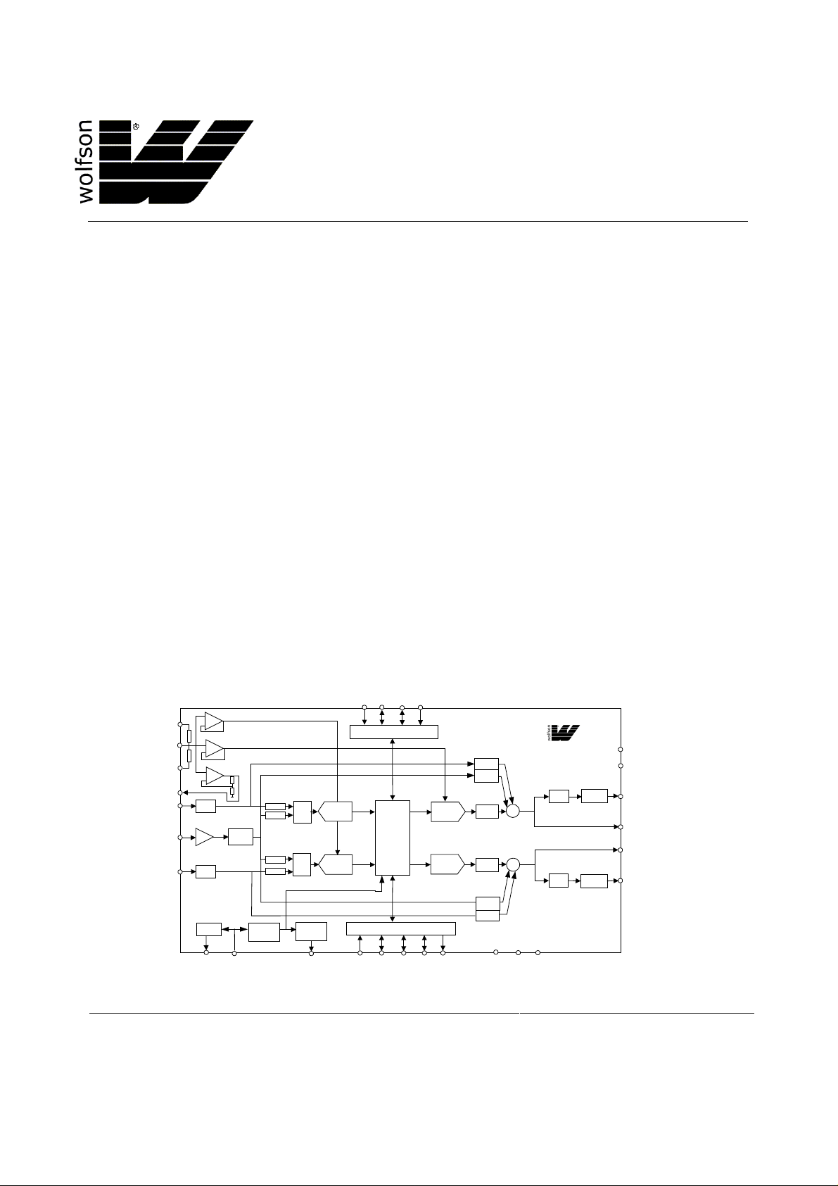
BLOCK DIAGRAM
AVDD
VMID
AGND
MICBIAS
RLINEIN
MICIN
LLINEIN
VOL
+12 to -34.5dB,
1.5dB Steps
VOL
+12 to -34.5dB,
1.5dB Steps
OSC
XTO
0dB/
20dB
XTI/MCLK
CLKIN
DIVIDER
(Div x1, x2)
MUTE
MUTE
MUTE
MUTE
MUX
MUX
CLKOUT
DIVIDER
(Div x1, x2)
CLKOUT
WOLFSON MICROELECTRONICS LTD
Lutton Court, Bernard Terrace, Edi nburgh, EH8 9NX, UK
Tel: +44 (0) 131 667 9386
Fax: +44 (0) 131 667 5176
Email: [email protected]
www.wolfsonmicro.com
CONTROL INTERFACE
ADC
ADC
DIGTAL AUDIO INTERFACE
SCLK
MODE
SDIN
CSB
Bypass
MUTE
ATTEN/
MUTE
Side Tone
MUTE
DAC
DIGITAL
FILTERS
DAC
MUTE
Side Tone
ATTEN/
MUTE
MUTE
Bypass
DACDAT
BCLK
DACLRC
ADCDAT
ADCLRC
(1.5V)
DCVDD
WM8731
+6 to -73dB
1 dB Steps
VOL/
MUTE
Σ
Σ
VOL/
MUTE
+6 to -73dB
1 dB Steps
DGND
(3.3V)
DBVDD
H/P
DRIVER
H/P
DRIVER
HPVDD
HPGND
RHPOUT
ROUT
LOUT
LHPOUT
Advanced Information data sheets
contain preliminary data on new products
in the preproduction phase of
development. Supplementary data will be
published at a later date.
2001 Wolfson Microelectronics Ltd.
Page 2

WM8731 Advanced Information
TABLE OF CONTENTS
DESCRIPTION.......................................................................................................1
FEATURES............................................................................................................1
APPLICATIONS.....................................................................................................1
BLOCK DIAGRAM.................................................................................................1
PIN CONFIGURATION ..........................................................................................6
ORDERING INFORMATION..................................................................................6
PIN DESCRIPTION................................................................................................6
ABSOLUTE MAXIMUM RATINGS.........................................................................7
RECOMMENDED OPERATING CONDITIONS.....................................................7
ELECTRICAL CHARACTERISTICS......................................................................8
TERMINOLOGY...................................................................................................10
POWER CONSUMPTION....................................................................................11
MASTER CLOCK TIMING...................................................................................12
DIGITAL AUDIO INTERFACE – MASTER MODE 13
DIGITAL AUDIO INTERFACE – SLAVE MODE 14
MPU INTERFACE TIMING 15
DEVICE DESCRIPTION.......................................................................................17
INTRODUCTION 17
AUDIO SIGNAL PATH 18
LINE INPUTS ..........................................................................................................................................18
MICROPHONE INPUT ............................................................................................................................ 20
MICROPHONE BIAS...............................................................................................................................21
ADC.........................................................................................................................................................22
ADC FILTERS......................................................................................................................................... 23
DAC FILTERS......................................................................................................................................... 23
DAC......................................................................................................................................................... 24
LINE OUTPUTS ......................................................................................................................................24
HEADPHONE AMPLIFIER......................................................................................................................26
BYPASS MODE ...................................................................................................................................... 28
SIDETONE MODE...................................................................................................................................29
DEVICE OPERATION 30
DEVICE RESETTING.............................................................................................................................. 30
CLOCKING SCHEMES...........................................................................................................................30
CORE CLOCK.........................................................................................................................................30
CRYSTAL OSCILLATOR........................................................................................................................31
WOLFSON MICROELECTRONICS LTD AI Rev 2.0 February 2001
2
Page 3

WM8731 Advanced Information
CLOCKOUT ............................................................................................................................................31
DIGITAL AUDIO INTERFACES.............................................................................................................. 32
MASTER AND SLAVE MODE OPERATION.......................................................................................... 35
AUDIO DATA SAMPLING RATES 36
NORMAL MODE SAMPLE RATES........................................................................................................37
128/192fs NORMAL MODE.................................................................................................................... 39
512/768fs NORMAL MODE.................................................................................................................... 39
USB MODE SAMPLE RATES.................................................................................................................40
ACTIVATING DSP AND DIGITAL AUDIO INTERFACE 41
SOFTWARE CONTROL INTERFACE 41
SELECTION OF SERIAL CONTROL MODE.......................................................................................... 41
3-WIRE (SPI COMPATIBLE) SERIAL CONTROL MODE......................................................................42
2-WIRE SERIAL CONTROL MODE........................................................................................................42
POWER DOWN MODES 43
REGISTER MAP 45
DIGITAL FILTER CHARACTERISTICS...............................................................50
TERMINOLOGY 50
DAC FILTER RESPONSES.................................................................................51
ADC FILTER RESPONSES.................................................................................52
ADC HIGH PASS FILTER 53
DIGITAL DE-EMPHASIS CHARACTERISTICS...................................................54
RECOMMENDED EXTERNAL COMPONENTS..................................................55
PACKAGE DIMENSIONS....................................................................................56
WOLFSON MICROELECTRONICS LTD AI Rev 2.0 February 2001
3
Page 4

WM8731 Advanced Information
TABLE OF FIGURES
Figure 1 System Clock Timing Requirements............................................................................12
Figure 2 Clock Out Timing Requirements...................................................................................12
Figure 3 Master Mode Connection ..............................................................................................13
Figure 4 Digital Audio Data Timing – Master Mode ...................................................................13
Figure 5 Slave Mode Connection.................................................................................................14
Figure 6 Digital Audio Data Timing – Slave Mode......................................................................14
Figure 7 Program Register Input Timing - 3-Wire MPU Serial Control Mode..........................15
Figure 8 Program Register Input Timing – 2-Wire MPU Serial Control Mode .........................16
Figure 9 Line Input Schematic.....................................................................................................18
Figure 10 Line Input Application Drawing ..................................................................................19
Figure 11 Microphone Input Schematic......................................................................................20
Figure 12 Microphone Input and Bias Application Drawing .....................................................21
Figure 13 Microphone Bias Schematic .......................................................................................22
Figure 14 Multi-Bit Oversampling Sigma Delta ADC Schematic...............................................22
Figure 15 ADC Digital Filter..........................................................................................................23
Figure 16 DAC Filter Schematic...................................................................................................23
Figure 17 Multi-Bit Oversampling Sigma Delta Schematic.......................................................24
Figure 18 Line Output Schematic ................................................................................................25
Figure 19 Line Outputs Application Drawing .............................................................................26
Figure 20 Headphone Amplifier Schematic................................................................................26
Figure 21 Headphone Output Application Drawing...................................................................28
Figure 22 Signal Routing in Bypass Mode...................................................................................28
Figure 23 Side Tone Mode Schematic.........................................................................................29
Figure 24 Crystal Oscillator Application Circuit..........................................................................31
Figure 25 Left Justified Mode........................................................................................................32
Figure 26 I2S Mode........................................................................................................................33
Figure 27 Right Justified Mode.....................................................................................................33
Figure 28 DSP Mode.......................................................................................................................33
Figure 29 Master Mode .................................................................................................................36
Figure 30 Slave Mode.....................................................................................................................36
Figure 31 3-Wire Serial Interface...................................................................................................42
Figure 32 2-Wire Serial Interface..................................................................................................42
Figure 33 DAC Digital Filter Frequency Response –Type 0.......................................................51
Figure 34 DAC Digital Filter Ripple –Type 0.................................................................................51
Figure 35 DAC Digital Filter Frequency Response –Type 1.......................................................51
Figure 36 DAC Digital Filter Ripple –Type 1.................................................................................51
Figure 37 DAC Digital Filter Frequency Response –Type 2.......................................................51
Figure 38 DAC Digital Filter Ripple –Type 2.................................................................................51
Figure 39 DAC Digital Filter Frequency Response –Type 3.......................................................52
Figure 40 DAC Digital Filter Ripple –Type 3.................................................................................52
Figure 41 ADC Digital Filter Frequency Response –Type 0.......................................................52
Figure 42 ADC Digital Filter Ripple –Type 0.................................................................................52
Figure 43 ADC Digital Filter Frequency Response –Type 1.......................................................52
Figure 44 ADC Digital Filter Ripple –Type 1.................................................................................52
Figure 45 ADC Digital Filter Frequency Response –Type 2.......................................................53
Figure 46 ADC Digital Filter Ripple –Type 2.................................................................................53
Figure 47 ADC Digital Filter Frequency Response –Type 3.......................................................53
Figure 48 ADC Digital Filter Ripple –Type 3.................................................................................53
Figure 49 De-Emphasis Frequency Response (32kHz) ..............................................................54
Figure 50 De-Emphasis Error (32kHz)..........................................................................................54
Figure 51 De-Emphasis Frequency Response (44.1kHz) ...........................................................54
Figure 52 De-Emphasis Error (44.1kHz).......................................................................................54
Figure 53 De-Emphasis Frequency Response (48kHz) ..............................................................54
Figure 54 De-Emphasis Error (48kHz)..........................................................................................54
Figure 55 External Components Diagram....................................................................................55
WOLFSON MICROELECTRONICS LTD AI Rev 2.0 February 2001
4
Page 5

WM8731 Advanced Information
TABLE OF TABLES
Table 1 Powerdown Mode Current Consumption Examples....................................................11
Table 2 Line Input Software Control............................................................................................19
Table 3 Microphone Input Software Control...............................................................................21
Table 4 ADC Software Control .....................................................................................................22
Table 5 ADC Software Control .....................................................................................................23
Table 6 DAC Software Control .....................................................................................................24
Table 7 Output Software Control.................................................................................................25
Table 8 Headphone Output Software Control ............................................................................27
Table 9 Bypass Mode Software Control......................................................................................29
Table 10 Side Tone Mode Table...................................................................................................29
Table 11 Software Control of Reset.............................................................................................30
Table 12 Software Control of Core Clock....................................................................................30
Table 13 Programming CLKOUT..................................................................................................31
Table 14 Digital Audio Interface Control.....................................................................................35
Table 15 Programming Master/Slave Modes..............................................................................35
Table 16 Sample Rate Control......................................................................................................37
Table 17 Normal Mode Sample Rate Look-up Table..................................................................38
Table 18 Normal Mode Actual Sample Rates..............................................................................39
Table 19 128fs Normal Mode Sample Rate Look-up Table........................................................39
Table 20 USB Mode Sample Rate Look-up Table.......................................................................40
Table 21 USB Mode Actual Sample Rates ..................................................................................41
Table 22 Activating DSP and Digital Audio Interface.................................................................41
Table 23 Control Interface Mode Selection.................................................................................41
Table 24 2-Wire MPU Interface Address Selection.....................................................................42
Table 25 Power Conservation Modes Software Control ...........................................................43
Table 26 Standby Mode ................................................................................................................44
Table 27 Poweroff Mode ...............................................................................................................45
Table 28 Mapping of Program Registers.....................................................................................45
Table 29 Register Map Description..............................................................................................50
Table 30 Digital Filter Characteristics .........................................................................................50
WOLFSON MICROELECTRONICS LTD AI Rev 2.0 February 2001
5
Page 6
WM8731 Advanced Information
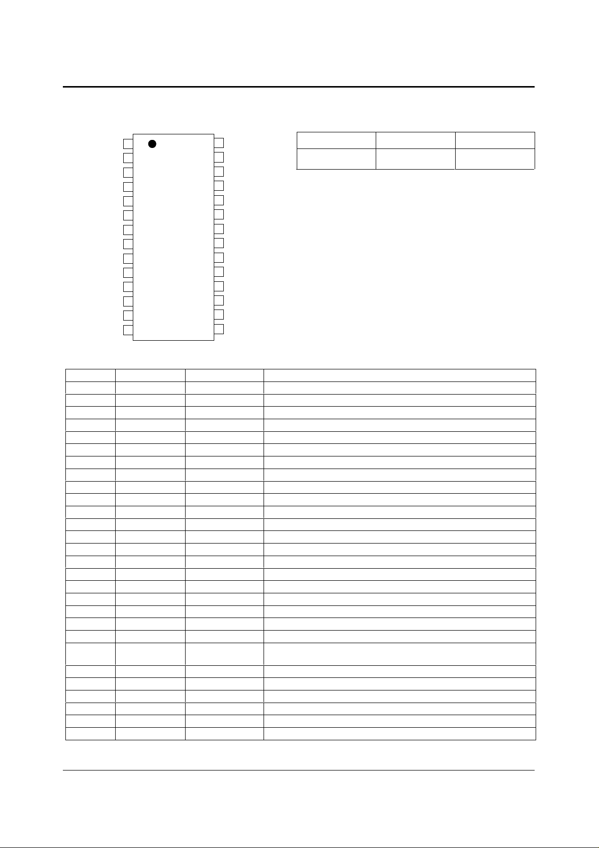
PIN CONFIGURATION ORDERING INFORMATION
DBVDD
CLKOUT
BCLK
DACDAT
DACLRC
ADCDAT
ADCLRC
HPVDD
LHPOUT
RHPOUT
HPGND
LOUT
ROUT
AVDD
1
2
3
4
5
6
7
8
9
10
11
12
13
14
15
28
27
26
25
24
23
22
21
20
19
18
17
16
DGND
DCVDD
XTO
XTI/MCLK
SCLK
SDIN
CSB
MODE
LLINEIN
RLINEIN
MICIN
MICBIAS
VMID
AGND
DEVICE TEMP. RANGE PACKAGE
XWM8731EDS -10 to +70oC 28-pin SSOP
PIN DESCRIPTION
PIN NAME TYPE DESCRIPTION
1 DBVDD Supply
2 CLKOUT Digital Out put
3 BCLK Digital Input/Output
4 DACDAT Digital Input
5 DACLRC Digital Input/Output
6 ADCDAT Digital Output
7 ADCLRC Digital Input/Output
8 HPVDD Supply
9 LHPOUT Analogue Output
10 RHPOUT Analogue Output
11 HPGND Ground
12 LOUT Analogue Output
13 ROUT Analogue Output
14 AVDD Supply
15 AGND Ground
16 VMI D Analogue Output
17 MICBIAS Analogue Output
18 MICIN Analogue Input
19 RLINEIN Analogue Input
20 LLI NE IN Analogue Input
21 MODE Digital Input
22 CSB Digital Input
23 SDIN Digital Input /Output
24 SCLK Digital Input
25 XTI/MCLK Digital Input
26 XTO Digital Output
27 DCVDD Supply
28 DGND Ground
Note:
1. Pull Up/Down only present when Control Register Int erface ACTIVE=0 to conserve power.
Digital Buffers VDD
Buffered Clock Output
Digital Audio Bit Cloc k, Pull Down, (see Note 1)
DAC Digital Audio Data Input
DAC Sample Rate Left/Right Clock, Pull Down (see Note 1)
ADC Digital Audio Data Output
ADC Sample Rate Left/Right Clock, Pull Down (see Note 1)
Headphone VDD
Left Channel Headphone Output
Right Channel Headphone Output
Headphone GND
Left Channel Line Output
Right Channel Line Output
Analogue VDD
Analogue GND
Mid-rail reference decoupling point
Electret Microphone Bias
Microphone Input (AC coupled)
Right Channel Line Input (AC coupled)
Left Channel Line Input (AC coupled)
Control Interface Selec tion, Pull Up (see Note 1)
3-Wire MPU Chip Selec t/ 2-Wire MPU interface address selecti on,
active low, Pull up (see Note 1)
3-Wire MPU Data Input / 2-Wire MPU Data Input
3-Wire MPU Clock I nput / 2-Wire MPU Cloc k Input
Crystal Input or Master Cloc k Input (MCLK)
Crystal Output
Digital Core VDD
Digital GND
WOLFSON MICROELECTRONICS LTD AI Rev 2.0 February 2001
6
Page 7
WM8731 Advanced Information
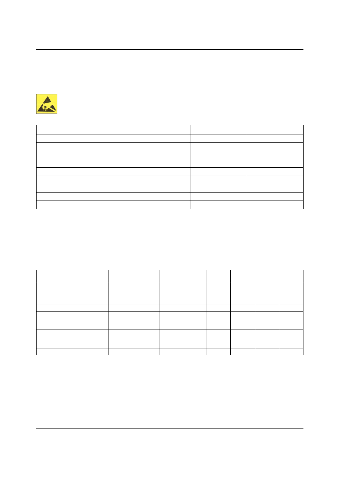
ABSOLUTE MAXIMUM RATINGS
Absolute Maximum Ratings are stress ratings only. Permanent damage to the devi ce may be caused by continuously operating at
or beyond these limits. Device functional operating lim its and guaranteed performance spec ifications are given under Elect rical
Characteristics at the test conditions s pecified
ESD Sensitive Device. This device is manufac tured on a CMOS proces s. It is theref ore genericall y suscept ible
to damage from excessi ve st atic volt ages. Proper E SD precaut ions m ust be tak en during handling and st orage
of this device.
CONDITION MIN MAX
Digital supply voltage
Analogue supply voltage
Voltage range digital inputs
Voltage range analogue inputs
Master Clock Frequency (see Note 4)
Operating temperature range, T
Storage temperature
Package body temperature (s ol deri ng 10 seconds)
Package body temperature (s ol deri ng 2 minutes)
Notes:
1. Analogue and digital grounds mus t always be within 0.3V of each other.
2. The digital supply core voltage (DCV DD) must always be less than or equal to the analogue supply voltage (AVDD) or
digital supply buffer volt age (DBVDD).
3. The digital supply buffer volt age (DB VDD) must always be less t han or equal to the analogue supply voltage (AVDD).
4. When CLKIDIV2=1
A
-0.3V +3.63V
-0.3V +3.63V
DGND -0.3V DVDD +0.3V
AGND -0.3V AVDD +0. 3V
40MHz
-10°C+70°C
-65°C +150°C
+240°C
+183°C
RECOMMENDED OPERATING CONDITIONS
PARAM ETER SYMBOL TEST
Digital supply range (Core)
Digital supply range (Buffer)
Analogue supply range
Ground
Total analogue supply current
Digital supply current
Standby Current Consumption
DCVDD 1.42 3.6 V
DBVDD 2.7 3.6 V
AVDD, HPVDD 2.7 3.6 V
DGND,AGND,HPGND 0 V
IAVDD, IHPVDD DCVDD, DBVDD,
IDCVDD, IDBVDD DCVDD, DBVDD,
CONDITIONS
AVDD,
HPVDD= 3.3V
AVDD,
HPVDD= 3.3V
MIN TYP MAX UNIT
13 mA
3mA
10 uA
WOLFSON MICROELECTRONICS LTD AI Rev 2.0 February 2001
7
Page 8

WM8731 Advanced Information
.7 x DBVDD
.9 x DBVDD
ELECTRICAL CHARACTERISTICS
Test Conditions
AVDD, HPVDD, DBVDD = 3. 3V , AGND = 0V, DCVDD = 1.5V, DGND = 0V, T
256fs unless otherwise stated.
PARAM ETER SYMBOL TEST
CONDITIONS
Digital Logic Levels (CMOS Levels)
Input LOW level V
Input HIGH level V
Output LOW V
Output HIGH V
IL
IH
OL
OH
Power On Reset Threshold (DCVDD)
DCVDD Threshold On -> Off V
Hysteresis V
DCVDD Threshold Off -> On V
th
IH
OL
Analogue Reference Levels
Reference voltage (VMID) V
Potential divider resis tance R
VMID
VMID
Line Input to ADC
Input Signal Level (0dB) V
SNR (Note 1,3)
INLINE
A-weighted, 0dB gain
@ fs = 48kHz
SNR (Note 1,3)
A-weighted, 0dB gain
@ fs = 96kHz
SNR (Note 1,3)
A-weighted, 0dB gain
@ fs = 48kHz, AVDD =
2.7V
Dynamic Range (Note 3) DR
A-weighted, -60dB full
scale input
THD
Power Supply Rejection Ratio
PSSR 1kHz 100mVpp 50 dB
-1dB input, 0dB gain -85 -80 dB
20Hz to 20kHz
100mVpp
ADC channel separation
Programmable Gain Maximum
Programmable Gain Minim um
Programmable Gain St ep S i ze
Mute attenuation
Input Resistance R
INLINE
1kHz input 90 dB
1kHz input
Rsource < 50 Ohms
Guaranteed Monotonic 1.5 dB
0dB, 1kHz input 80 dB
0dB gain 40k 50k Ohms
12dB gain 10k 20k Ohms
Input Capacitance C
INLINE
Microphone Input to ADC @ 0dB Gain, fs = 8kHz (40k ohm Source Impedance. See Figure 11)
Input Signal Level (0dB) V
SNR (Note 1,3)
Dynamic Range (Note 3) DR
INMIC
A-weighted, 0dB gain 85 90 dB
A-weighted, -60dB full
scale input
THD
Power Supply Rejection Ratio
PSSR 1kHz 100mVpp 50 dB
0dB input, 0dB gain -80 -75 dB
20Hz to 20kHz
100mVpp
= +25oC, Slave Mode, fs = 48kHz, XTI/MCLK =
A
MIN TYP MAX UNIT
.3 x DBVDD V
0.10 x
DBVDD
0.7 0.9 1.2 V
0.3 V
0.6 V
AVDD/2 –
50mV
AVDD/2 AVDD/2 +
50mV
40k 50k 60k Ohms
1.0
AVDD/3.3
93 97 dB
94 dB
90 dB
93 97 dB
45 dB
+12
-34.5
10 pF
1.0
AVDD/3.3
85 90 dB
45 dB
V
V
V
V
Vrms
dB
Vrms
WOLFSON MICROELECTRONICS LTD AI Rev 2.0 February 2001
8
Page 9

WM8731 Advanced Information
.75*AVDD –
Test Conditions
AVDD, HPVDD, DBVDD = 3. 3V , AGND = 0V, DCVDD = 1.5V, DGND = 0V, T
256fs unless otherwise stated.
PARAM ETER SYMBOL TEST
CONDITIONS
Programmable Gain Boost
Mic Path gain (MICBOOST gain
is additional to this nominal
gain)
Mute attenuation
Input Resistance
Input Capacitance
MICBOOST bit
set
R
INMIC
C
INMIC
1kHz input
Rsource < 50 Ohms
MICBOOST = 0
Rsource < 50 Ohms
0dB, 1kHz input 80 dB
Microphone Bias
Bias Voltage
Bias Current Source
Output Noise Voltage
V
MICBIAS
I
MICBIAS
Vn 1K to 20kHz 25 nV/√Hz
Line Output for DAC Playback Only (Load = 10k ohms. 50pF)
0dBfs Full scale output vol tage
SNR (Note 1,2,3)
At LINE outputs 1.0 x
A-weighted,
@ fs = 48kHz
SNR (Note 1,2,3)
A-weighted
@ fs = 96kHz
SNR (Note 1,2,3)
A-weighted,
@ fs = 48kHz, AVDD
= 2.7V
Dynamic Range (Note 3) DR
A-weighted, -60dB
full scale input
THD
1kHz, 0dBfs -88 -80 dB
1kHz, -3dBfs -92 -86 dB
Power Supply Rejection Ratio
PSSR 1kHz 100mVpp 50 dB
20Hz to 20kHz
100mVpp
DAC channel separation
Analogue Line Input to Line Output (Load = 10k ohms. 50pF, No Gain on Input ) Bypass Mode
0dB Full scale output voltage
SNR (Note 1, 3)
THD
1kHz, 0dB -86 -80 dB
1kHz, -3dB -92 -86 dB
Power Supply Rejection Ratio
PSSR 1kHz 100mVpp 50 dB
20Hz to 20kHz
100mVpp
Mute attenuation
1kHz, 0dB 80 dB
Stereo Headphone Output
0dB Full scale output voltage
Max Output Power RL = 32
P
O
ohms
Max Output Power RL = 16
P
O
ohms
= +25oC, Slave Mode, fs = 48kHz, XTI/MCLK =
A
MIN TYP MAX UNIT
34 dB
14 dB
8k 10k 12k Ohms
10 pF
0.75*AVDD .75*AVDD +
100mV
100mV
3mA
Vrms
AVDD/3.3
90 100 dB
98 dB
93 dB
85 90 dB
45 dB
100 dB
1.0 x
Vrms
AVDD/3.3
90 95 dB
45 dB
1.0 x
Vrms
AVDD/3.3
30 mW
40 mW
V
WOLFSON MICROELECTRONICS LTD AI Rev 2.0 February 2001
9
Page 10

WM8731 Advanced Information
Test Conditions
AVDD, HPVDD, DBVDD = 3. 3V , AGND = 0V, DCVDD = 1.5V, DGND = 0V, T
256fs unless otherwise stated.
PARAM ETER SYMBOL TEST
CONDITIONS
SNR (Note 3)
THD
Power Supply Rejection Ratio
PSSR 1kHz 100mVpp 50 dB
A-weighted 90 97 dB
1kHz, RL = 32 ohms @
P
= 10mW rm s
O
1kHz, R
= 32 ohms @
L
= 20mW rm s
P
O
20Hz to 20kHz
100mVpp
Programmable Gain Maximum
1kHz 6
Programmable Gain Minim um
Programmable Gain St ep S i ze
Mute attenuation
1kHz 1 dB
1kHz, 0dB 80 dB
Microphone Input to Headphone Output Side Tone Mode
0dB Full scale output voltage
SNR (Note 1, 3)
Power Supply Rejection Ratio
PSSR 1kHz 100mVpp 50 dB
20Hz to 20kHz
100mVpp
Programmable Att enuat i on
1kHz 15
Maximum
Programmable Att enuat i on
Minimum
Programmable Att enuat i on Step
1kHz 3 dB
Size
Mute attenuation
1kHz, 0dB 80 dB
Notes:
1. Ratio of output level with 1kHz ful l scale input, to the output l evel with t he input short circuited, measured ‘A’ weighted
over a 20Hz to 20kHz bandwidth using an Audio analyser.
2. Ratio of output level with 1kHz ful l scale input, to the output l evel with al l zeros into the digital input, measured ‘A’
weighted over a 20Hz to 20kHz bandwidth.
3. All performance m easurements done with 20kHz low pass fil ter, and where noted an A-weight filter. Failure to use
such a filter will result in higher THD+N and lower SNR and Dynamic Range readings than are found in t he E l ectrical
Characteristics. The l ow pass filter removes out of band noi se; although it is not audible i t may affect dynam i c
specification values.
4. VMID decoupled with 10uF and 0.1uF capacitors (smaller values may res ul t in reduced performance).
= +25oC, Slave Mode, fs = 48kHz, XTI/MCLK =
A
MIN TYP MAX UNIT
0.1
60
dB
1.0
40
dB
45 dB
dB
-73
1.0 x
Vrms
AVDD/3.3
90 95 dB
45 dB
dB
6
%
%
TERMINOLOGY
1. Signal-to-noise ratio (dB) - SNR is a measure of the dif ference in level between the full s cale output and the output
with no signal applied. (No Auto-zero or Automute function is employed in achieving these resul ts).
2. Dynamic range (dB) - DR is a measure of the difference between the highest and lowest portions of a signal.
Normally a THD+N measurem ent at 60dB below full scale. The measured signal is then correct ed by addi ng the 60dB
to it. (e.g. THD+N @ -60dB= -32dB, DR= 92dB ).
3. THD+N (dB) - THD+N is a ratio, of the rms values, of (Noise + Dis t ortion)/Signal.
4. Channel Separation (dB) - Also known as Cross-Talk. This is a measure of the am ount one channel is isolat ed from
the other. Normally measured by sending a full scale si gnal down one channel and measuring the other.
WOLFSON MICROELECTRONICS LTD AI Rev 2.0 February 2001
10
Page 11
WM8731 Advanced Information
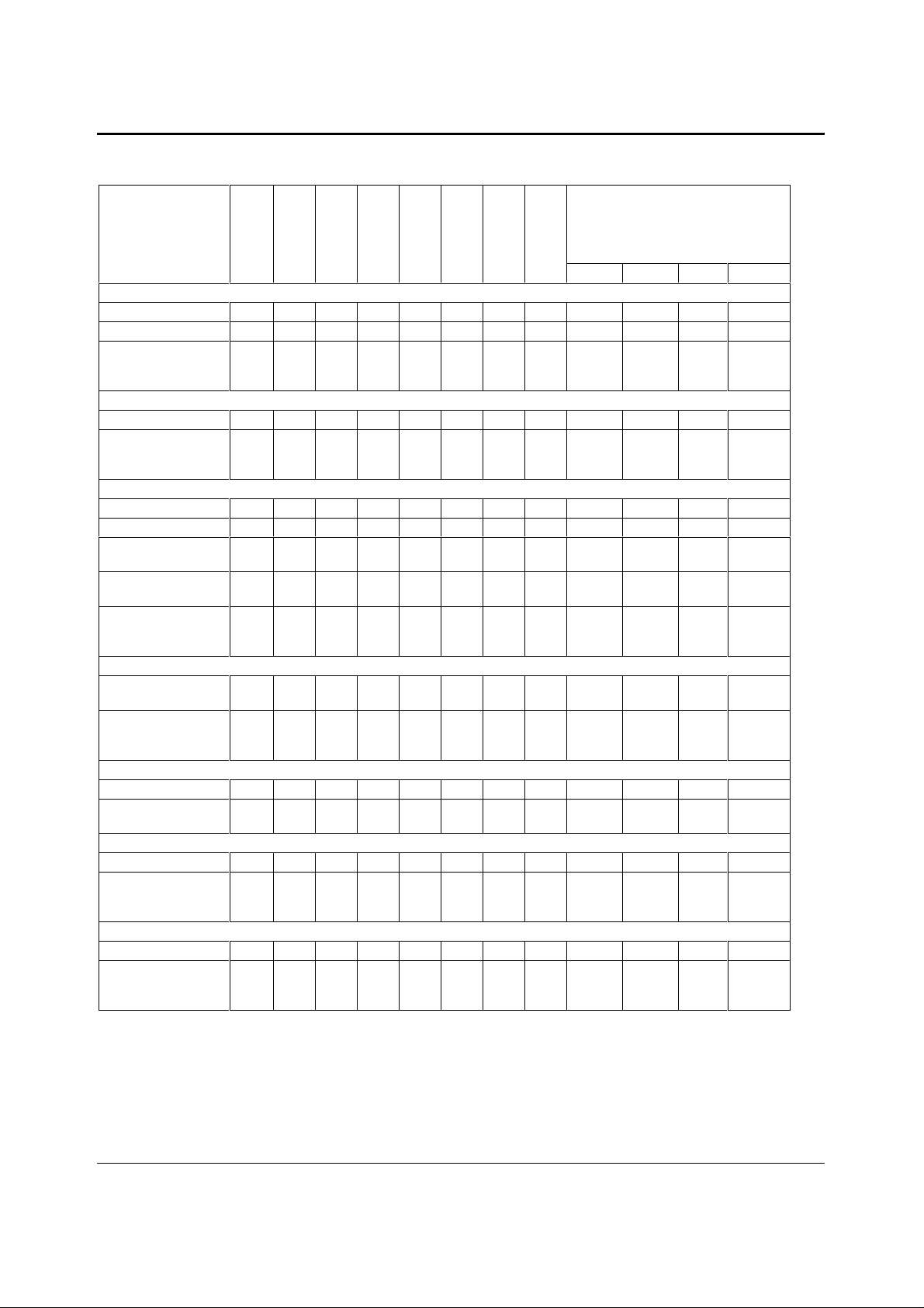
POWER CONSUMPTION
DESCRIPTION
OUTPD
OSCPD
CLKOUTPD
POWEROFF
Record and Playback
All active
Oscillator disabled
Oscillator and
CLKOUT disabled,
No microphone
Playback Only
Playback Only
Playback Only
Oscillator and
CLKOUT disabled
Record Only
Record Only
Line Record Only
Record Only,
Oscillator disabled
Microphone Record
Only,
Microphone Record
Only, Oscillator
disabled
Side Tone
Microphone to
Headphone Out
Microphone to
Headphone Out,
Oscillator disabled
Analogue Bypass
Line In to Line Out
Line In to Line Out,
Oscillator disabled
Standby
Standby
Standby, Oscillator
and CLKOUT
disabled
Power Down
Power Down
Power Down,
Oscillator and
CLKOUT disabled
Table 1 Powerdown Mode Current Consumption Examples
Notes:
1. AVDD, HPVDD, DBVDD = 3. 3V , AGND = 0V, DCVDD = 1.5V, DGND = 0V, T
XTI/MCLK = 256fs (12.288MHz).
2. All figures are quiescent , with no signal.
3. The power dissipation in the headphone itself not included in the above table.
00000000 13TBDmA
00100000 12 mA
01100010 11 mA
00000111 7TBDmA
01100111 6 mA
00011000 9 mA
00011010 8 mA
00111010 7 mA
00011001 9 mA
00111001 8 mA
00001101 3 mA
00101101 2 mA
00001110 3 mA
00101110 2 mA
00011111 1.5TBDmA
01111111 0.05 mA
100X11XX 1.5 mA
1 1 1 X 1 1 X X 0.01 TBD mA
DACPD
MICPD
ADCPD
CURRENT CONSUMPTIONMODE
LINEINPD
MIN TYP MAX UNITS
= +25oC. Slave Mode, fs = 48kHz,
A
WOLFSON MICROELECTRONICS LTD AI Rev 2.0 February 2001
11
Page 12
WM8731 Advanced Information
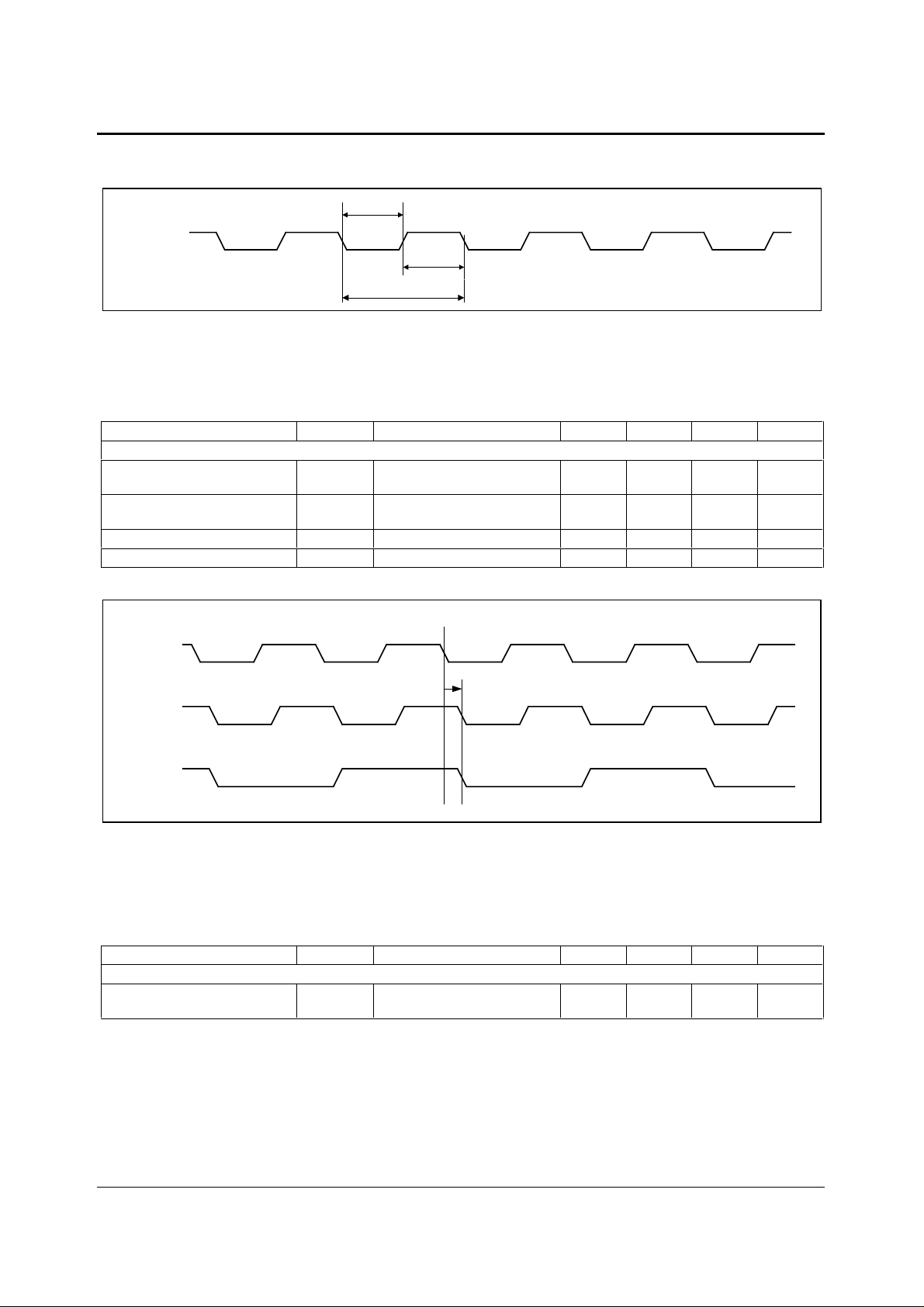
MASTER CLOCK TIMING
t
XTIL
XTI/MCLK
t
XTIH
t
XTIY
Figure 1 System Clock Timing Requirements
Test Conditions
AVDD, HPVDD, DBVDD = 3. 3V , AGND = 0V, DCVDD = 1.5V, DGND = 0V, T
256fs unless otherwise stated.
PARAMETER SYMBOL TEST CONDITIONS MIN TYP MAX UNIT
System Clock Timing Information
XTI/MCLK System clock pulse width
high
XTI/MCLK System clock pulse width
low
XTI/MCLK System clock cycle time
XTI/MCLK Duty cycle
t
XTIH
t
XTIL
t
XTIY
= +25oC, Slave Mode fs = 48kHz, XTI/MCLK =
A
18 ns
18 ns
54 ns
40:60 60:40
XTI/MCLK
t
COP
CLKOUT
CLKOUT
(DIV X2)
Figure 2 Clock Out Timing Requirements
Test Conditions
AVDD, HPVDD, DBVDD = 3. 3V , AGND = 0V, DCVDD = 1.5V, DGND = 0V, T
= +25oC, Slave Mode fs = 48kHz, XTI/MCLK =
A
256fs unless otherwise stated.
PARAMETER SYMBOL TEST CONDITIONS MIN TYP MAX UNIT
System Clock Timing Information
CLKOUT propagation delay from
XTI/MCLK falling edge
t
COP
010ns
WOLFSON MICROELECTRONICS LTD AI Rev 2.0 February 2001
12
Page 13
WM8731 Advanced Information
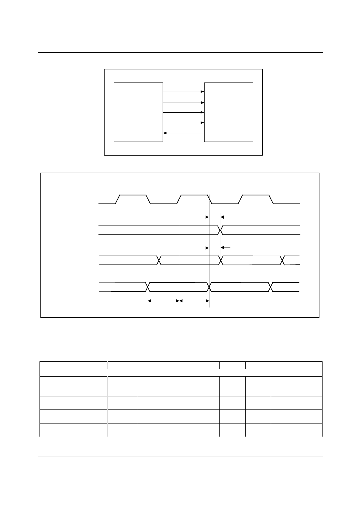
DIGITAL AUDIO INTERFACE – MASTER MODE
BCLK
BCLK
(Output)
ADCLRC/
DACLRC
(Outputs)
ADCDAT
ADCLRC
WM8731
CODEC
Note: ADC and DAC can run at different rates
Figure 3 Master Mode Connection
DACLRC
ADCDAT
DACDAT
DSP
ENCODER/
DECODER
t
DL
t
DDA
DACDAT
t
DST
Figure 4 Digital Audio Data Timing – Master Mode
Test Conditions
AVDD, HPVDD, DBDD = 3.3V , AGND = 0V, DCVDD = 1.5V, DGND = 0V, T
256fs unless otherwise stated.
PARAMETER SYMBOL TEST CONDITIONS MIN TYP MAX UNIT
Audio Data Input Timing Information
ADCLRC/DACLRC
propagation delay from
BCLK falling edge
ADCDAT propagation delay
from BCLK falling edge
DACDAT setup time to
BCLCK rising edge
DACDAT hold time from
BCLK rising edge
WOLFSON MICROELECTRONICS LTD AI Rev 2.0 February 2001
t
t
t
t
DL
DDA
DST
DHT
t
DHT
= +25oC, Slave Mode, fs = 48kHz, XTI/MCLK =
A
010ns
010ns
10 ns
10 ns
13
Page 14
WM8731 Advanced Information
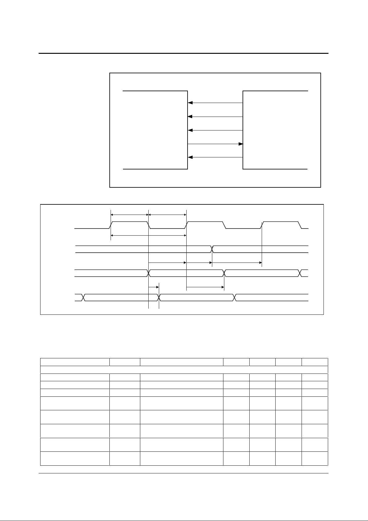
DIGITAL AUDIO INTERFACE – SLAVE MODE
BCLK
BCLK
DACLRC/
ADCLRC
DACDAT
ADCLRC
WM8731
CODEC
DACLRC
ADCDAT
DACDAT
Note: The ADC and DAC can run at different rates
Figure 5 Slave Mode Connection
t
BCH
t
BCY
t
BCL
t
DS
t
DD
t
LRH
DSP
ENCODER/
DECODER
t
LRSU
t
DH
ADCDAT
Figure 6 Digital Audio Data Timing – Slave Mode
Test Conditions
AVDD, HPVDD, DBVDD = 3. 3V , AGND = 0V, DCVDD = 1.5V, DGND = 0V, T
= +25oC, Slave Mode, fs = 48kHz, XTI/MCLK =
A
256fs unless otherwise stated.
PARAMETER SYMBOL TEST CONDITIONS MIN TYP MAX UNIT
Audio Data Input Timing Information
BCLK cycle time
BCLK pulse width high
BCLK pulse width low
DACLRC/ADCLRC set-up
t
BCY
t
BCH
t
BCL
t
LRSU
50 ns
20 ns
20 ns
10 ns
time to BCLK risi ng edge
DACLRC/ADCLRC hold
t
LRH
10 ns
time from BCLK ri sing edge
DACDAT set-up time to
t
DS
10 ns
BCLK rising edge
DACDAT hold time from
t
DH
10 ns
BCLK rising edge
ADCDAT propagation delay
t
DD
010ns
from BCLK falling edge
WOLFSON MICROELECTRONICS LTD AI Rev 2.0 February 2001
14
Page 15
WM8731 Advanced Information
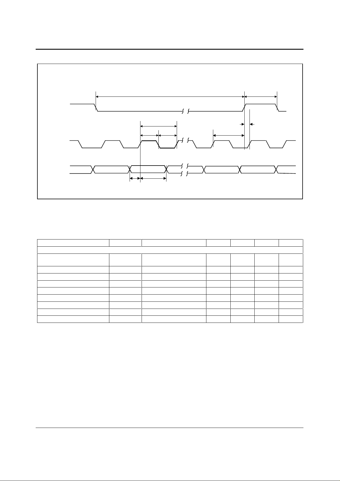
MPU INTERFACE TIMING
t
CSL
t
CSH
CSB
t
CSS
t
SCH
t
SCY
t
SCL
t
SCS
SCLK
SDIN
t
DSU
Figure 7 Program Register Input Timing - 3-Wire MPU Serial Control Mode
Test Conditions
AVDD, HPVDD, DBVDD = 3. 3V , AGND = 0V, DCVDD = 1.5V, DGND = 0V, T
256fs unless otherwise stated.
PARAMETER SYMBOL TEST CONDITIONS MIN TYP MAX UNIT
Program Register Input Information
SCLK rising edge to CSB ris i ng
t
SCS
edge
SCLK pulse cycle time
SCLK pulse width low
SCLK pulse width high
SDIN to SCLK set-up time
SCLK to SDIN hold time
CSB pulse width low
CSB pulse width high
CSB rising to SCLK ris i ng
t
t
t
t
t
t
t
t
SCY
SCL
SCH
DSU
DHO
CSL
CSH
CSS
t
DHO
A
LSB
= +25oC, Slave Mode, fs = 48kHz, XTI/MCLK =
60 ns
80 ns
20 ns
20 ns
20 ns
20 ns
20 ns
20 ns
20 ns
WOLFSON MICROELECTRONICS LTD AI Rev 2.0 February 2001
15
Page 16
WM8731 Advanced Information
SDIN
SCLK
t
3
t
6
t
1
t
2
t
10
t
5
t
7
t
3
t
4
t
8
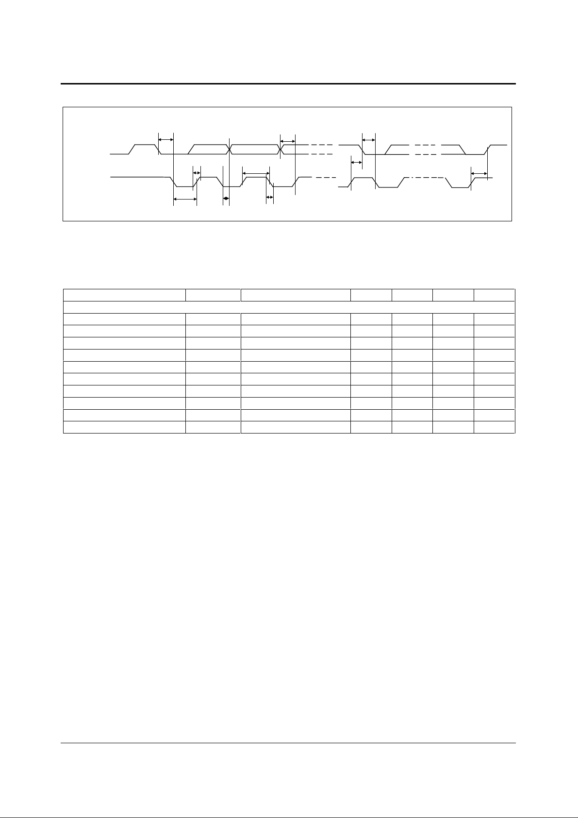
Figure 8 Program Register Input Timing – 2-Wire MPU Serial Control Mode
Test Conditions
AVDD, HPVDD, DBVDD = 3. 3V , AGND = 0V, DCVDD = 1.5V, DGND = 0V, T
= +25oC, Slave Mode, fs = 48kHz, XTI/MCLK =
A
256fs unless otherwise stated.
PARAMETER SYMBOL TEST CONDITIONS MIN TYP MAX UNIT
Program Register Input Information
SCLK Frequency
SCLK Low Pulsewidth
SCLK High Pulsewidth
Hold Time (Start Condition)
Setup Time (Start Condit i on)
Data Setup Time
SDIN, SCLK Rise Time
SDIN, SCLK Fall Time
Setup Time (Stop Condition)
Data Hold Time
t
1
t
2
t
3
t
4
t
5
t
6
t
7
t
8
t
10
0 400 kHz
600 ns
1.3 us
600 ns
600 ns
100 ns
300 ns
300 ns
600 ns
900 ns
WOLFSON MICROELECTRONICS LTD AI Rev 2.0 February 2001
16
Page 17

WM8731 Advanced Information
DEVICE DESCRIPTION
INTRODUCTION
The WM8731 is a low power audio CODEC designed speci fically for portable audio products. It ’s
features, performance and low power consumption make it ideal for portable MP3 players and
portable mini-disc pl ayers.
The CODEC includes line and mic rophone inputs to t he on-board ADC, line and headphone outputs
from the on-board DAC, a crystal os cillator, conf igurable digital audio int erface and a c hoice of 2 or 3
wire MPU control interface. It is fully com patible and an i deal partner for a range of industry s tandard
microprocessors , controllers and DSPs.
The CODEC includes three low noise inputs - mono mic rophone and stereo line. Line inputs have
+12dB to -34dB logarithmic volume level adjustm ents and mute. The Mic rophone input has -6dB to
34dB volume level adjustm ent. An electret mic rophone bias level is also available. All the required
input filtering is contained within the device with no external components requi red.
The on-board stereo analogue to digital converter (ADC) is of a high quality using a m ulti-bit highorder oversampling architecture delivering optim um performance with low power consumption. The
output from the ADC is available on the digital audio i nterface. The ADC inc ludes an optional digi tal
high pass filter to remove unwanted dc components from the audio signal.
The on-board digital to analogue converter (DAC) accepts digital audio from the digital audio
interface. Digital filter de-em phasis at 32kHz, 44.1kHz and 48kHz can be applied to t he digital data
under software control. The DAC employs a high quality multi-bit high-order oversampling
architecture to again deliver opti mum performance with low power consumption.
The DAC outputs, Microphone (SIDETONE) and Line Inputs (BYPASS) are available both at line
level and through a headphone amplifier capabl e of efficiently driving low impedance headphones .
The headphone output volume is adjust able in the analogue dom ain over a range of +6dB to –73dB
and can be muted.
The design of the WM8731 has given muc h attention to power consumption without c ompromising
performance. It includes the ability to power off s elective parts of the circ uitry under soft ware control,
thus conserving power. Nine separate power save modes be configured under software control
including a standby and power off mode.
Special techniques allow the audio to be muted and t he device safely placed into s tandby, sections
of the device powered off and volume levels adjusted without any audible clicks, pops or zipper
noises. Therefore standby and power off m odes maybe used dynamically under software control,
whenever recording or playing is not required.
The device caters for a number of different sampli ng rates including indus try standard 8kHz, 32k Hz,
44.1kHz, 48kHz, 88.2kHz and 96kHz. Addi tional ly, t he devic e has an A DC and DAC t hat c an operate
at different sample rates.
There are two unique schemes featured within the programmable sample rates of the WM8731:
Normal industry standard 256/384fs sampling mode may be used, with the added ability to mix
different sampling rates. Als o a s pecial USB m ode is i ncl uded, whereby all audio s am pling rat es c an
be generated from a 12.00MHZ USB cloc k. Thus, for example, the ADC can rec ord to the DSP at
44.1kHz and be played back from t he CODEC at 8kHz with no external digital signal proc essing
required. The digital filters used at for bot h record and playbac k are opt im i sed for eac h s am pli ng rat e
used.
The digitised output is available in a num ber of audio data format s I
which frame sync plus 2 data packed words are transm itted), MSB -First, lef t justif ied and MSB-First,
right justified. The digi t al audio interface can operate in both master or slave modes.
2
S, DSP Mode (a burst mode in
The software control uses either 2 or 3-wire MPU int erf ace.
A crystal oscillator is included on board the device. The device can generate the system master clock
or alternatively it can acc ept an external master clock from the audio system.
WOLFSON MICROELECTRONICS LTD AI Rev 2.0 February 2001
17
Page 18
WM8731 Advanced Information
AUDIO SIGNAL PATH
LINE INPUTS
The WM8731 provides Left and Right channel line input s (RLINEIN and LLINEIN). The inputs are
high impedance and low capacitanc e, thus ideally suit ed to receiving line level s ignals from external
hi-fi or audio equipment.
Both line inputs include i ndependent programmable volum e level adjustment s and ADC input mute.
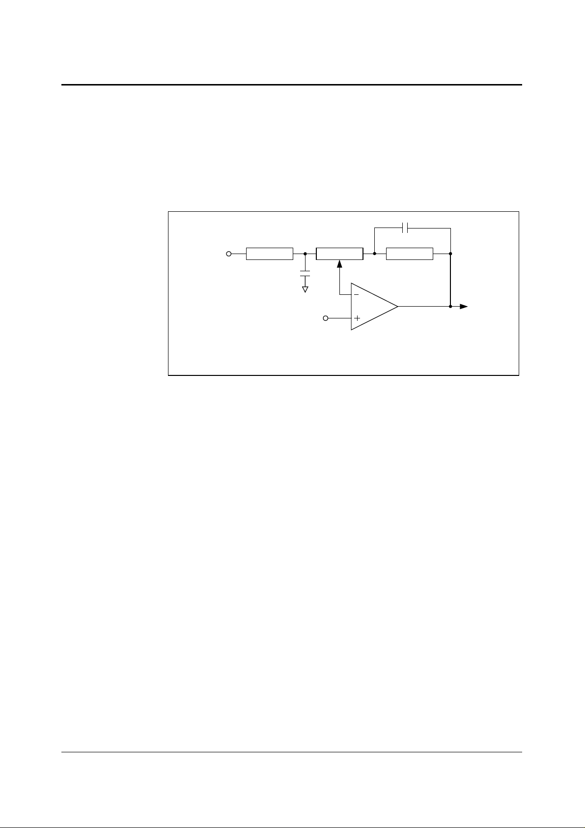
The scheme is illustrated in Figure 9. Passi ve RF and active Anti-Alias filters are also incorporat ed
within the line inputs. These prevent high frequencies aliasing into the audio band or otherwise
degrading performance.
LINEIN
12.5k
To
VMID
Figure 9 Line Input Schematic
The gain between the line inputs and the ADC is l ogarithm i cal ly adjust able f rom +12dB to –34.5dB in
1.5dB steps under software cont rol. The ADC Full Sc ale input is 1. 0V rms at AVDD = 3.3 volt s. Any
voltage greater than full scale will possibly overload the ADC and cause distort ion. Note that the full
scale input tracks directly with AVDD. The gain is independently adjustable on both Right and Left
Line Inputs. However, by setting the INBOTH bit whilst programming the volume control, both
channels are simultaneous ly updated with the same value. Use of INBOTH reduces the required
number of software writes required. The line inputs to the ADC can be mut ed in t he analogue dom ain
under software control. The software cont rol registers are shown Table 2. Note that the Line Input
Mute only mutes the input to the ADC, this will still allow the Line Input s ignal to pass to the line
output in Bypass Mode.
ADC
WOLFSON MICROELECTRONICS LTD AI Rev 2.0 February 2001
18
Page 19
WM8731 Advanced Information
REGISTER
ADDRESS
0000000
Left Line In
0000001
Right Line In
Table 2 Line Input Software Control
BIT LABEL DEFAULT DESCRIPTION
4:0 LINVOL[4:0] 10111
7 LINMUTE 1 Left Channel Line Input Mute to ADC
8 LRINBOTH 0 Left to Right Channel Line Input
4:0 RINVOL[4:0] 10111
7 RINMUTE 1 Right Channel Line Input Mute t o
8 RLINBOTH 0 Right to Left Channel Line I nput
( 0dB )
( 0dB )
Left Channel Line Input Volum e
Control
11111 = +12dB . . 1.5dB steps down
to 00000 = -34.5dB
1 = Enable Mute
0 = Disable Mute
Volume and Mute Data Load Control
1 = Enable Simultaneous Load of
LINVOL[4:0] and LINMUTE to
RINVOL[4:0] and RINMUTE
0 = Disable Simultaneous Load
Right Channel Line Input Volum e
Control
11111 = +12dB . .1.5dB steps down
to 00000 = -34.5dB
ADC
1 = Enable Mute
0 = Disable Mute
Volume and Mute Data Load Control
1 = Enable Simultaneous Load of
RINVOL[4:0] and RINMUTE to
LINVOL[4:0] and LINMUTE
0 = Disable Simultaneous Load
The line inputs are biased internally t hrough the operational amplifier to VMID. Whenever the line
inputs are muted or the devic e placed into standby mode, t he line inputs are k ept biased to VMID
using special anti-thum p c irc uitry. This reduces any audible c licks that may otherwise be heard when
re-activating the inputs.
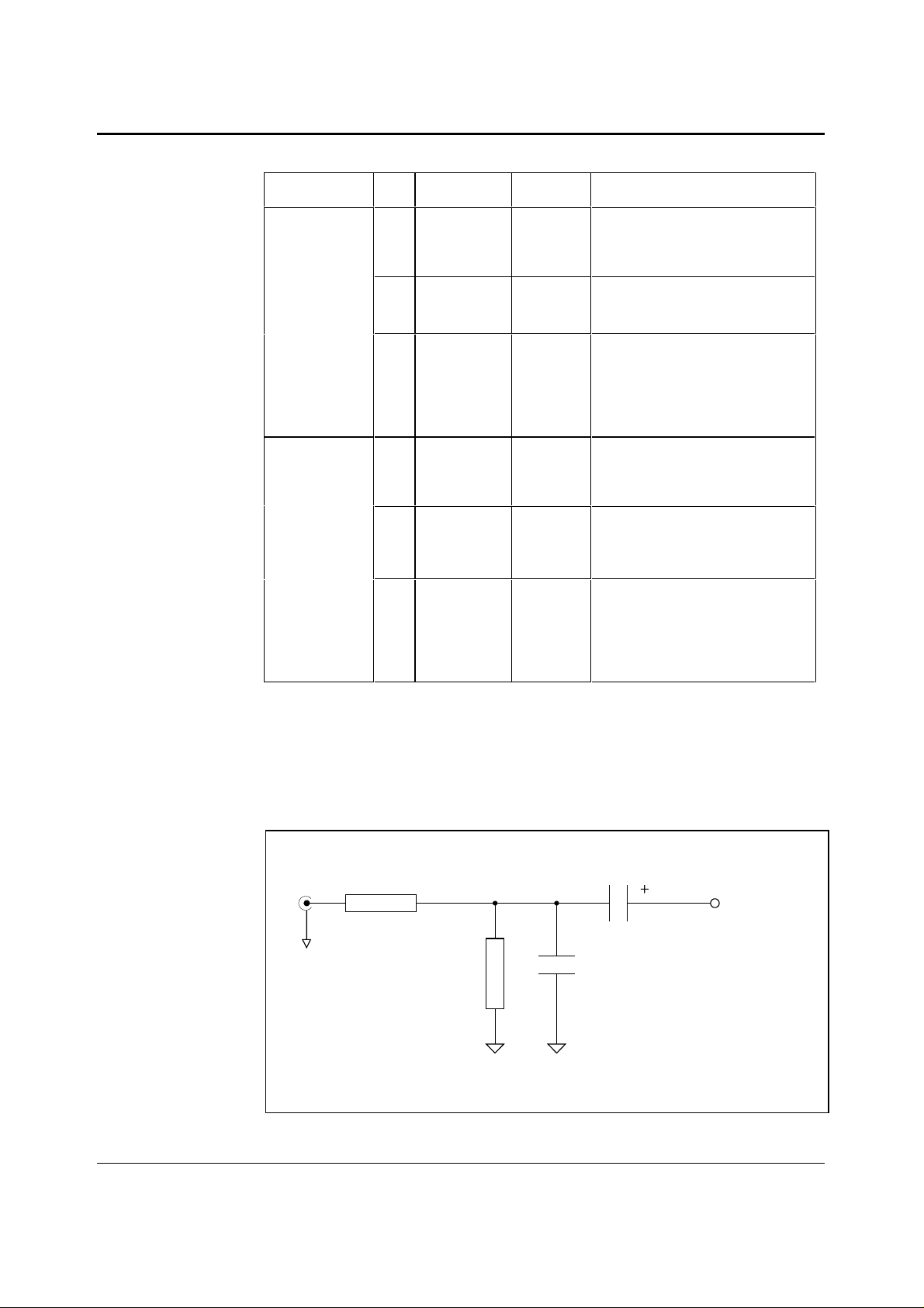
The external components required to complete the line input applicat i on i s shown in the Figure 10.
R1
C2
LINEIN
AGND
R2
C1
AGND AGND
Figure 10 Line Input Application Drawing
WOLFSON MICROELECTRONICS LTD AI Rev 2.0 February 2001
19
Page 20
WM8731 Advanced Information
For interfacing to a typical CD system, it is recom m ended that the input is sc aled t o ensure t hat t here
is no clipping of the signal . R1 = 5.6k, R2 = 5.6k, C1 = 220pF, C2 = 1µF.
R1 and R2 form a resistive divi der to attenuate the 2 Vrms output from a CD player t o a 1 Vrms level,
so avoiding overloading the inputs. R2 also provides a discharge path for C2, thus preventing the
input to C2 charging to an excessive vol t age whic h may otherwise damage any equipment connected
that is not suitably protected agains t high voltages. C1 forms an RF l ow pass filter f or increasing the
rejection of RF interference pi cked up on any cables. C2 form s a DC blocking capacitor to rem ove
the DC path between the WM8731 and the driving audio equipment. C2 together with the input
impedance of the WM8731 form a high pass fil ter.
MICROPHONE INPUT
MICIN is a high impedance, low capacitance input suitable for connection to a wide range of
monophonic microphones of different dynamics and sensitivities.
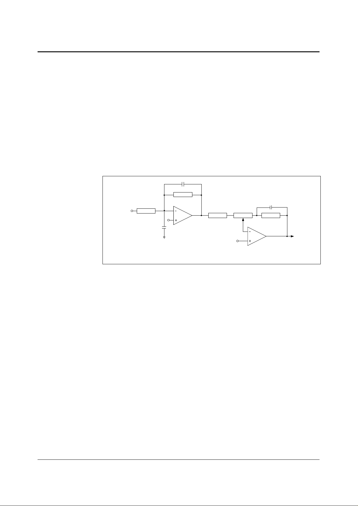
The MICIN includes programmable volum e adjustment s and a mute funct ion. The schem e is shown
in Figure 11. Passive RF and acti ve Anti-Alias filters are als o incorporated within the m icrophone
inputs. These allow a matched interface to the multi-bit oversampling ADC and preventing high
frequencies aliasing into the audio band or otherwise degrading performance.
50k
20dB GAIN BOOST
MICIN
10k
VMID
VMID
To
ADC
Figure 11 Microphone Input Schematic
There are 2 stages of gain made up of t wo low noise invert i ng operational amplifiers.
st
The 1
stage comprises a nominal gain of G1 = 50k/10k = 5. B y adding an external resis tor (Rmic) in
series with MICIN the gain of st age can be adjusted. For example adding Rm ic = 40K set s the gain
of stage 1 to x1 (0dB). The equation below can be used to c al culate the gain versus Rmi c.
G1 = 50k/ (Rmic + 10k)
Or alternatively to calculate the value of Rmic to ac hieve a given gain, G1.
Rmic = (50k/G1) – 10k
The internal 50k and 10k resistors have a tolerance of 15% . For Rmicext = 90k G = 0.5 (-6dB) and
for Rmicext = 0 G = x10 (14dB).
nd
The 2
stage comprises a 0dB gain s tage t hat c an be sof tware confi gured to provide a f ixed 20dB of
gain for low sensitivity m i crophones.
The microphone input can therefore be configured with a variable gain of between -6dB and 14dB on
st
the 1
stage, and an additional fixed 0dB or 20dB on the 2nd stage. This allows for all gains to the
input signal in the range –6dB to 34dB t o be catered for.
The ADC Full Scale input is 1.0V rms at AVDD = 3.3 vol ts. Any voltage greater than full s cale will
possibly overload the ADC and cause distortion. Note that the full scale input tracks directly with
AVDD. Stage 1 and Stage 2 gains should be configured so that the ADC receives a m aximum signal
equal to its full sc al e for maximising the signal to noise.
The software control for the MICIN is shown in Table 3. Note that t he Microphone Mute only mutes
the input to the ADC, this will still allow the Microphone Input signal t o pass to the line output in
Sidetone Mode.
WOLFSON MICROELECTRONICS LTD AI Rev 2.0 February 2001
20
Page 21
WM8731 Advanced Information
REGISTER
ADDRESS
0000100
Analogue Audio
Path Control
Table 3 Microphone Input Software Control
The microphone input is biased internally through t he operational amplifier to VMID. W henever the
line inputs are muted the MICIN input is kept biased t o VMID using spec ial anti-thum p circuit ry. This
reduces any audible clicks that may otherwise be heard when re-activating the input.
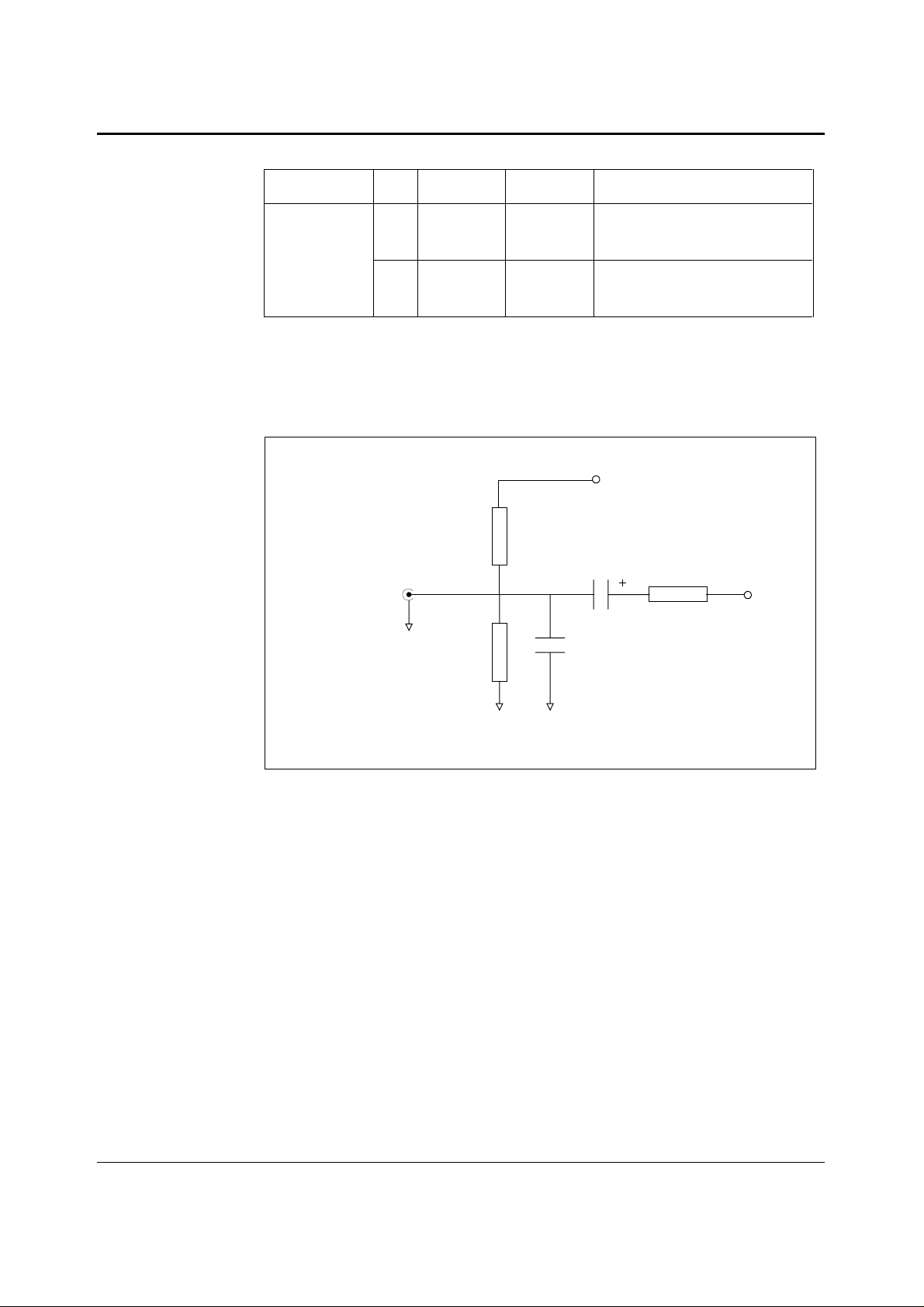
The application drawing for the microphone i s shown in Figure 12.
FROM
MICROPHONE
BIT LABEL DEFAULT DESCRIPTION
0 MICBOOST 0 Microphone Input Level Boost
1 = Enable Boost
0 = Disable Boost
1 MUTEMIC 1 Line Input Mute to ADC
1 = Enable Mute
0 = Disable Mute
MICBIAS
R1
C2
Rmic
MICIN
AGND
Figure 12 Microphone Input and Bias Application Drawing
Recommended com ponent values are C1 = 220pF (npo c eramic), C2 = 1µF, R1 = 680 ohms, R2 =
47k. Rmic values depends on gain setting (see above).
R1 and R2 form part of the biasing network (refer to Microphone Bias sect ion below). R1 connected
to MICBIAS is neces sary only for electret type mic rophones that require a voltage bias. R2 s hould
always be present to prevent the microphone input from charging to a high voltage which may
damage the microphone on connec tion. R1 and R2 s hould be large so as not to attenuate the s ignal
from the microphone, which can have source impedance greater than 2k. C1 together with the
source impedance of the microphone and the input im pedance of MICIN forms an RF filter. C2 is a
DC blocking capacitor t o allow the microphone to be biased at a dif ferent DC voltage to the MICI N
signal.
R2
AGND AGND
C1
MICROPHONE BIAS
The MICBIAS output provides a low noise reference voltage suitable for biasing electret type
microphones and the assoc iated external resistor biasing network. Refer to the Microphone Input
section for an applicati on drawing and further description.
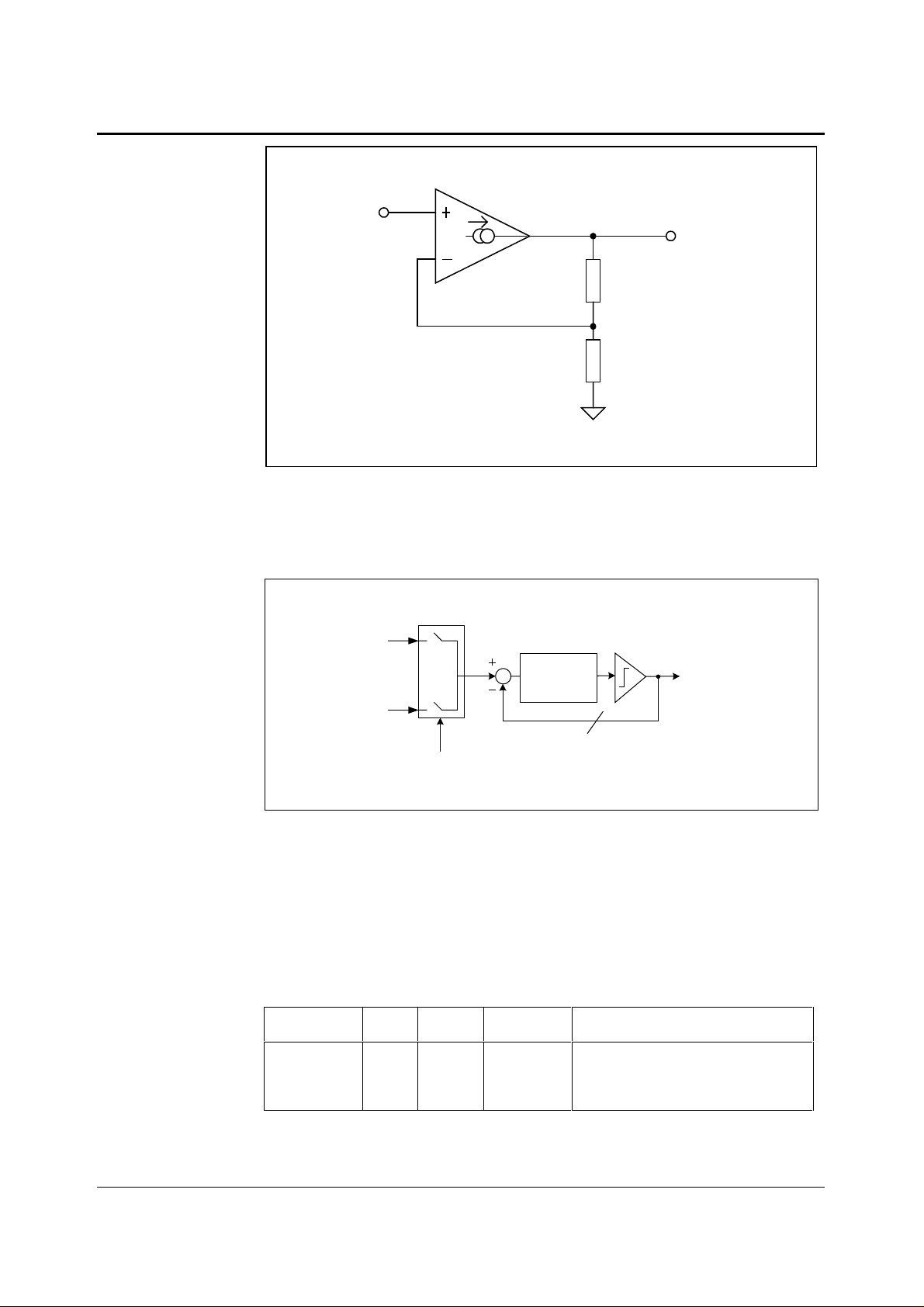
The scheme for MICBIAS is shown in Figure 13. Note that there is a maximum source current
capability of 3mA available for the MICBIAS. This limits the smallest value of external biasing
resistors that can safely be used.
Note that the MICBIAS out put is not active in st andby mode.
WOLFSON MICROELECTRONICS LTD AI Rev 2.0 February 2001
21
Page 22
WM8731 Advanced Information
VMID
MICBIAS
R2R
AGND
Figure 13 Microphone Bias Schematic
ADC
The WM8731 uses a multi-bit oversampled sigma-delta ADC. A single channel of the ADC is
illustrated in the Figure 14.
FROM MICROPHONE
INPUT
FROM LINE INPUT
INSEL
ANALOG
INTEGRATOR
MULTI
BITS
TO ADC DIGITAL FILTERS
Figure 14 Multi-Bit Oversampling S igma Delta ADC Schematic
The use of multi-bit feedback and high oversampling rates reduces the effects of jitter and high
frequency noise.
The ADC Full Scale input is 1.0V rms at AVDD = 3.3 vol ts. Any voltage greater than full s cale will
possibly overload the ADC and cause distortion. Note that the full scale input tracks directly with
AVDD.
The device employs a pair of ADCs. The input can be selected f rom either the Line Inputs or the
Microphone input under software control. The two channels cannot be selected independent ly. The
control is shown in Table 4.
REGISTER
BIT LABEL DEFAULT DESCRIPTION
ADDRESS
0000100
Analogue
Audio Path
2 INSEL 0 Microphone/Line Input S el ect to ADC
1 = Microphone Input Select to ADC
0 = Line Input Select to ADC
Control
Table 4 ADC Software Control
The digital data from the A DC i s fed for signal processi ng t o the ADC Filters.
WOLFSON MICROELECTRONICS LTD AI Rev 2.0 February 2001
22
Page 23
WM8731 Advanced Information
ADC FILTERS
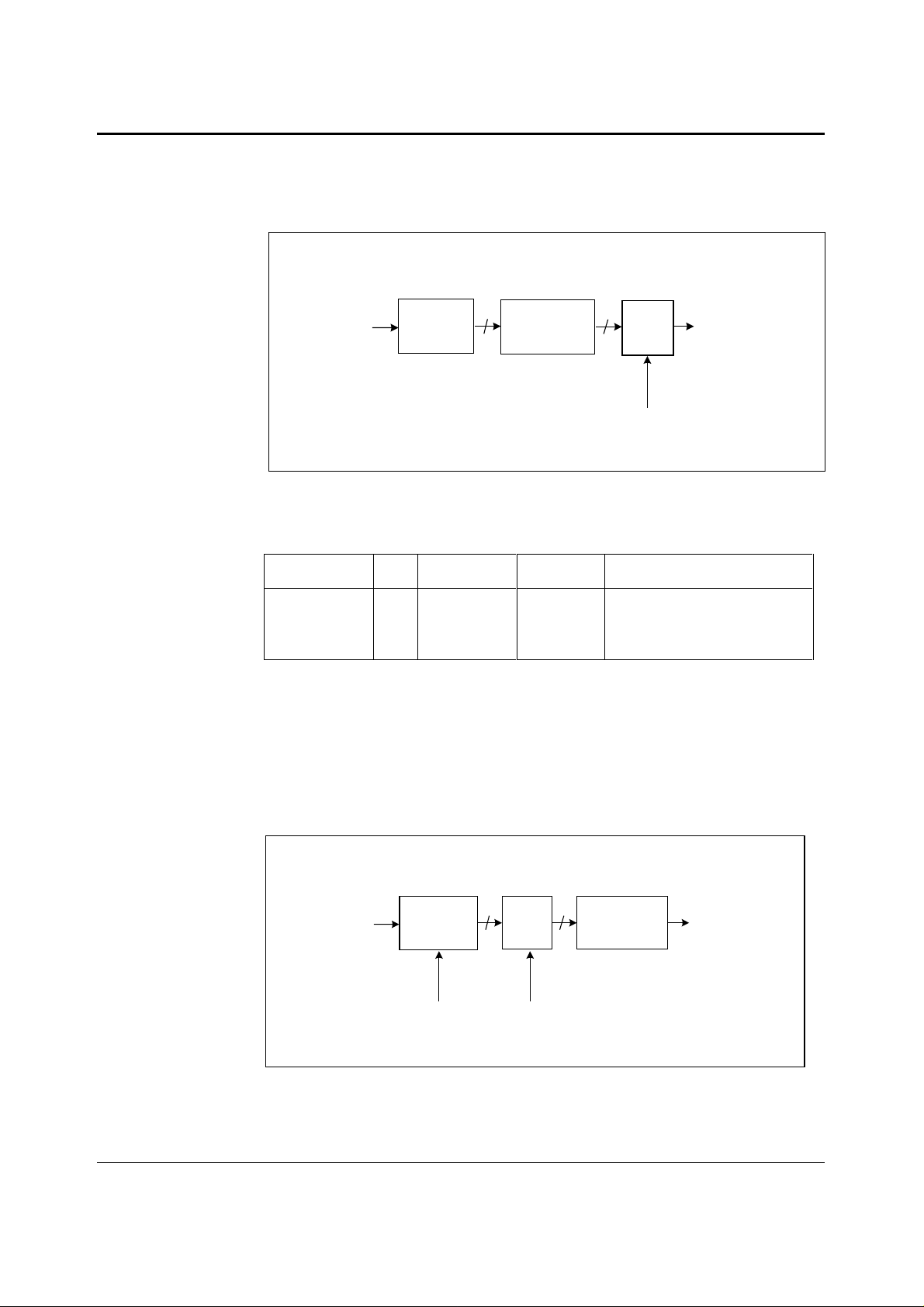
The ADC filters perform true 24 bit signal processing to convert the raw mul ti-bit oversampled data
from the ADC to the correc t sam pling f requency to be output on the digital audio interf ace. Figure 15
illustrates the digital filter path.
TO DIGITAL
AUDIO
INTERFACE
FROM ADC
DIGITAL
DECIMATOR
DIGITAL
DECIMATION
FILTER
DIGITAL
HPF
HPFEN
Figure 15 ADC Digital Filter
The ADC digital filters c ontai n a digit al high pas s f ilt er, s elec table vi a s oft ware cont rol. The high-pas s
filter response detailed in Di gi tal Filter Characteristics. The software control is shown in Table 5.
REGISTER
BIT LABEL DEFAULT DESCRIPTION
ADDRESS
0000101
Digital Audio
Path Control
0 ADCHPD 0 ADC High Pass Filter Enabl e
(Digital)
1 = Enable High Pass Filter
0 = Disable High Pass Filter
Table 5 ADC Software Control
There are several types of ADC filt ers, frequenc y and phase respons es of t hese are s hown in Digi tal
Filter Characteristics. The filter types are automatically configured depending on the sample rate
chosen. Refer to the sample rate section for more details.
DAC FILTERS
The DAC filters perform t rue 24 bit signal proc essing to c onvert the incom ing digital audio data from
the digital audio interface at the specified sam pl e rate to multi-bit oversampled data f or processing by
the analogue DAC. Figure 16 illustrates the DAC digit al f ilter path.
FROM DIGITAL
AUDIO
INTERFACE
DIGITAL
DE_EMPHASIS
MUTE
DIGITAL
INTERPOLATION
FILTER
TO LINE
OUTPUTS
DEEMP DACMU
Figure 16 DAC Filter Schematic
WOLFSON MICROELECTRONICS LTD AI Rev 2.0 February 2001
23
Page 24
WM8731 Advanced Information
The DAC digital filter can apply digital de-emphasis under soft ware control, as shown in Table 6.The
DAC can also perform a sof t mute where the audio data is digit ally brought to a mute l evel. This
removes any abrupt step changes in the audio that might otherwise result in audible clicks in the
audio outputs.
REGISTER
ADDRESS
0000101
Digital
Audio Path
Control
Table 6 DAC Software Control
BIT LABEL DEFAULT DESCRIPTION
2:1 DEEMP[1:0] 00 De-emphasis Control
(Digital)
11 = 48kHz
10 = 44.1kHz
01 = 32kHz
00 = Disable
3 DACMU 1 DAC Soft Mute Control
(Digital)
1 = Enable soft mute
0 = Disable soft mut e
DAC
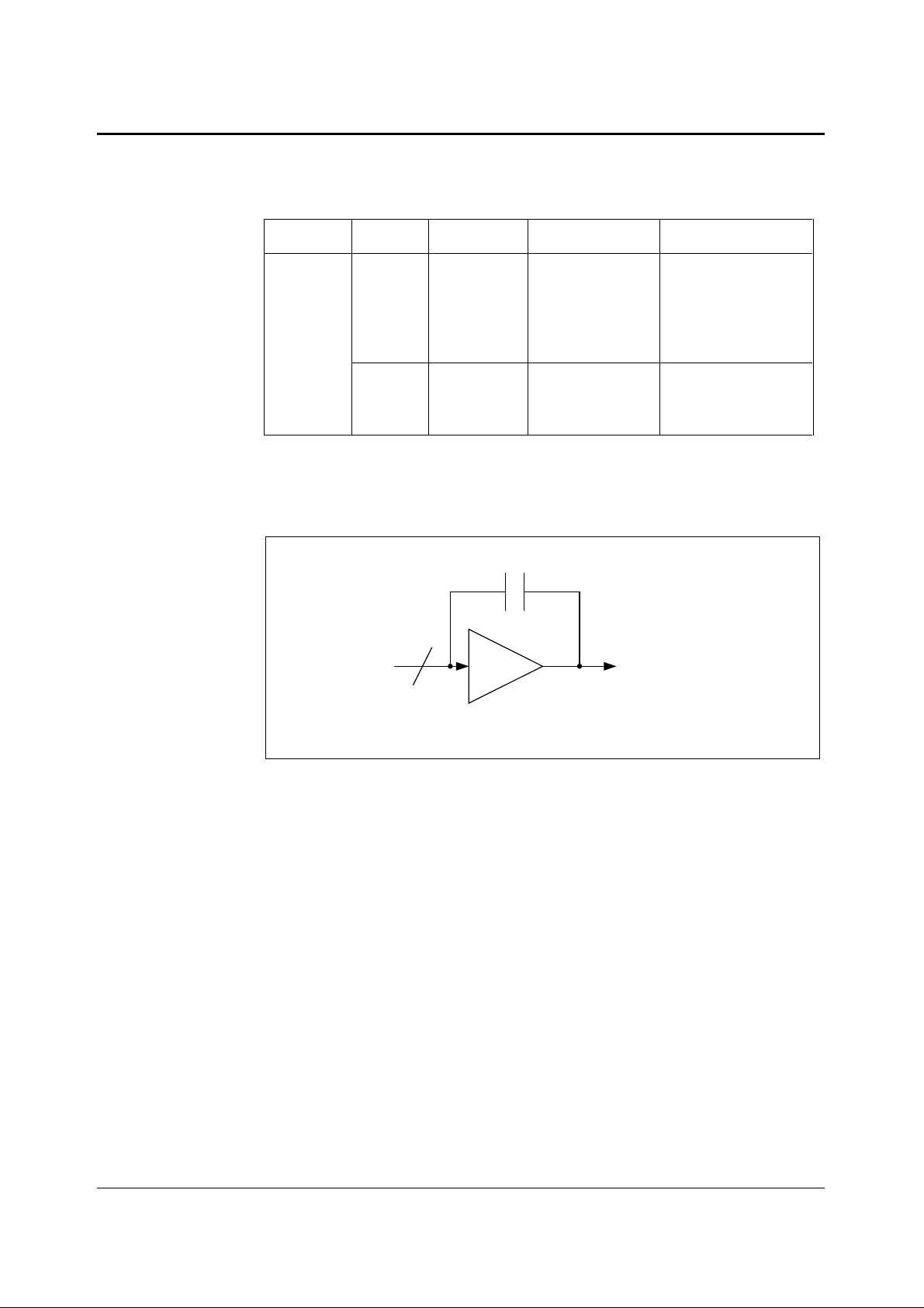
The WM8731 employs a multi-bit sigma delta oversampling digital to analogue converter. The
scheme for the converter is illustrated in Figure 17.
FROM DAC
DIGITAL
TO LINE OUTPUT
FILTERS
Figure 17 Multi-Bit Oversampling Sigma Delta Schematic
The DAC converts the multi-level digital audio data stream from the DAC digital filters into high
quality analogue audio.
LINE OUTPUTS
The WM8731 provides two low impedance line outputs LLINEOUT and RLINEOUT, suitable for
driving typical line loads of impedance 10K and capacitance 50pF. The line output is used to
selectively sum t he outputs from the DAC or/and the Line inputs in bypass m ode.
The LLINEOUT and RLINEOUT outputs are only avail able at a line output level and are not level
adjustable in the analogue domain, having a fixed gain of 0dB. The level is fixed suc h that at the DAC
full scale level the output level is Vrms at AVDD = 3.3 volts. Note that the DAC full scale level tracks
directly with AVDD. The scheme is shown in Figure 18. The line output incl udes a low order audio
low pass filter for removing out-of band com ponents from the sigm a-delta DAC. Theref ore no further
external filtering is required in m ost applications.
WOLFSON MICROELECTRONICS LTD AI Rev 2.0 February 2001
24
Page 25
WM8731 Advanced Information
SIDETONE
FROM MICRO P HO NE
INPUT
BYPASS
FROM LINE
INPUTS
DACSEL
FROM DAC
VMID
LINEOUT
TO HEADPHONE AMP
Figure 18 Line Output Schematic
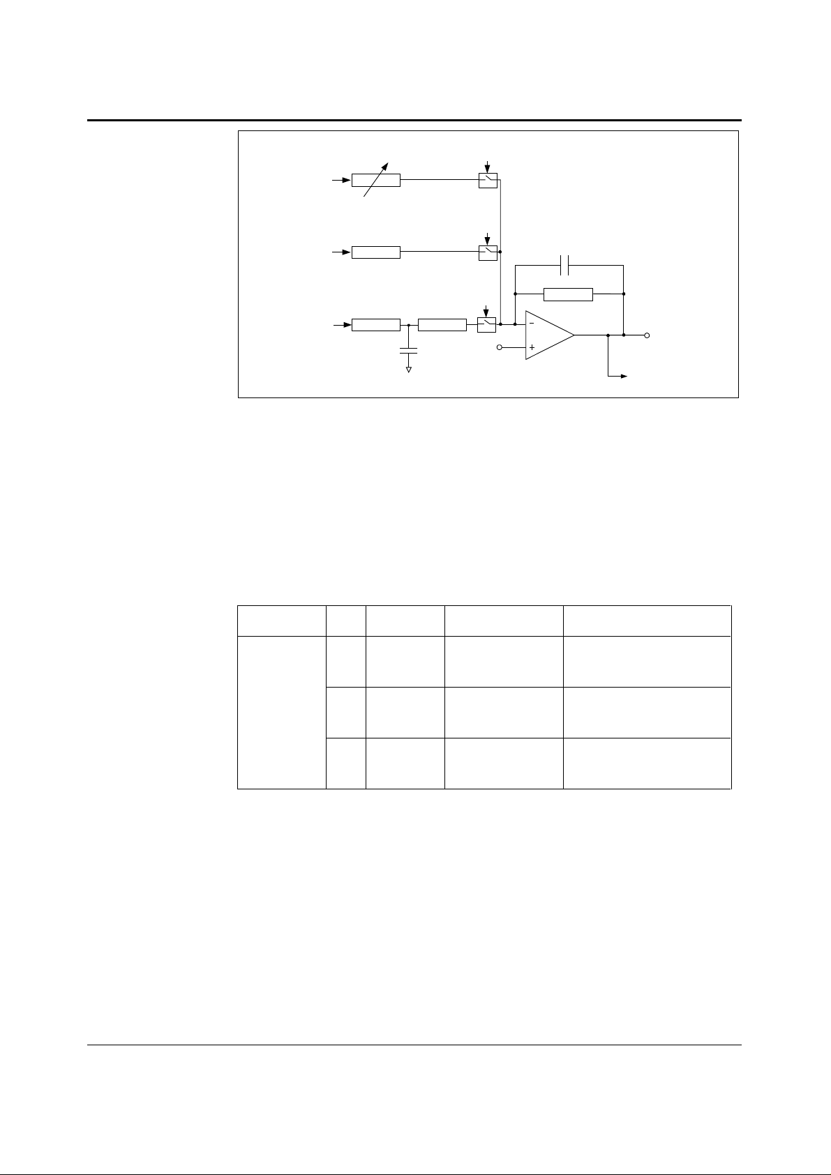
The DAC output, Line Input and m i crophone are summed into the Li ne Output. In DAC mode only the
output from the DAC is routed to the line out puts. In Bypass mode the Li ne Input is sum med int o the
Line Outputs. In Side Tone mode the Microphone Input is summed into the Line Output. These
features can be used for either over-dubbing or, i f the DAC is m uted, as a pure analogue bypass or
Side Tone feature, so avoiding any digit al signal processing.
The line output is muted by either muti ng the DAC (analogue) or Soft Muting (digital) and di sabling
the BYPASS and SIDETONE paths. Refer to the DAC sec tion for m ore details. W henever the DA C
is muted or the device plac ed into standby m ode the DC vol tage is maintai ned at t he line out puts to
prevent any audible clicks from being present.
The software control for the line output s is shown in Table 7.
REGISTER
BIT LABEL DEFAULT DESCRIPTION
ADDRESS
0000100
Analogue
Audio Path
Control
3 BYPASS 1
4 DACSEL 0
Bypass Switch
1 = Enable Bypass
0 = Disable Bypass
DAC Select
1 = Select DAC
0 = Don’t select DAC
5SIDETONE 0
Side Tone Switch
1 = Enable SideTone
0 = Disable Side Tone
Table 7 Output Software Control
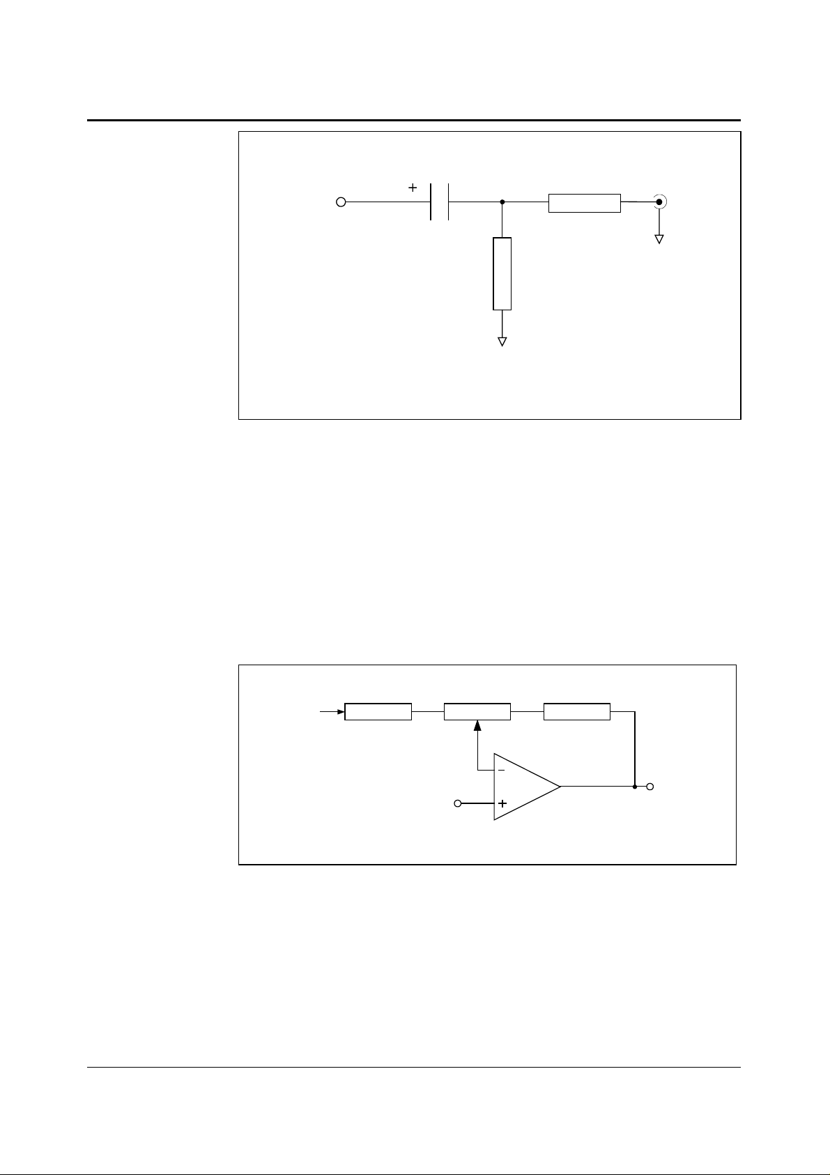
The recommended external components are shown in Figure 19.
WOLFSON MICROELECTRONICS LTD AI Rev 2.0 February 2001
25
Page 26
WM8731 Advanced Information
R2
LINEOUT
C1
R1
AGND
AGND
Figure 19 Line Outputs Application Drawing
Recommended values are C1 = 10µF, R1 = 47k, R2 = 100 ohms.
C1 forms a DC blocking c apacitor t o the line out puts. R1 prevents the out put volt age from dri fting so
protecting equipment connected to the line output. R2 forms a de-coupling resistor preventing
abnormal loads from dis turbing the device. Note that poor choice of diel ectric material for C1 can
have dramatic effect s on the measured signal dis tortion at the output
HEADPHONE AMPLIFIER
The WM8731 has a stereo headphone output available on LHPOUT and RHPOUT. The output is
designed specifically for driving 16 or 32 ohm headphones with maximum effici ency and low power
consumption. The headphone output includes a high quality volume level adjustment and mute
function.
The scheme of the circ ui t is shown in Figure 20.
FROM
DAC VIA
LINEOUT
HPOUT
VMID
Figure 20 Headphone Amplifier Schematic
LHPOUT and RHPOUT volumes can be independently adjusted under software control us ing the
LHPVOL[6:0] and RHPVOL[6:0] bits respectively of the headphone output control registers. The
adjustment is logari thmic with an 80dB range in 1dB steps from +6dB to –73dB.
The headphone outputs can be separately muted by writing codes less than 0110000 to
LHPVOL[6:0] or RHPVO[6:0]L bits. Whenever the headphone outputs are muted or the device
placed into standby mode, the DC voltage is maintained at t he line outputs to prevent any audible
clicks from being present.
WOLFSON MICROELECTRONICS LTD AI Rev 2.0 February 2001
26
Page 27

WM8731 Advanced Information
A zero cross detect c ircui t is provided at the i nput to t he headphones under the c ontrol of the LZCEN
and RZCEN bits of the headphone output c ontrol register. Using these cont rols the volume control
values are only updated when the input signal to t he gai n stage is close to the analogue ground level .
This minimis es and audible clicks and zipper noise as the gai n values are changed or the device
muted. Note that this circuit has no time out so if only DC levels are bei ng applied to the gain stage
input of more than approximately 20mV, then t he gain will not be updated. This zero cross func tion is
enabled when the LZCEN and RZCEN bit is set high during a volume register write. If there is
concern that a DC level may have bl ocked a volume c hange (one made with LZCEN or RZCEN set
high) then a subsequent volume write of the same value, but with the LZCEN or RZCEN bit set low
will force a volume update, regardless of the DC level.
LHPOUT and RHPOUT volume and zero-cross s etting can be changed independently. A lternatively,
the user can lock the two channels together, allowing both to be updated s imul taneously, halving the
number of serial writes required, provided that the sam e gain is needed for both channels. This is
achieved through writing to the HPBOTH bit of the cont rol regist er. Sett ing LRHPBOTH whils t writing
to LHPVOL and LZCEN will simultaneously update the Right Headphone controls similarly. The
corresponding effect on updati ng RLHP BOTH is also achieved.
The software control is given in Table 8.
REGISTER
ADDRESS
0000010
Left
Headphone
Out
0000011
Right
Headphone
Out
Table 8 Headphone Output Software Control
BIT LABEL DEFAULT DESCRIPTION
6:0 LHPVOL[6:0] 1111001
( 0dB )
7 LZCEN 0 Left Channel Zero Cross detect
8 LRHPBOTH 0 Left to Right Channel Headphone
6:0 RHPVOL[6:0] 1111001
( 0dB )
7 RZCEN 0 Right Channel Zero Cross Detect
8 RLHPBOTH 0 Right to Left Channel Headphone
Left Channel Headphone Output
Volume Control
1111111 = +6dB
. . 1dB steps down to
0110000 = -73dB
0000000 to 0101111 = MUTE
Enable
1 = Enable
0 = Disable
Volume, Mute and Zero Cross Data
Load Control
1 = Enable Simultaneous Load of
LHPVOL[6:0] and LZCEN to
RHPVOL[6:0] and RZCEN
0 = Disable Simultaneous Load
Right Channel Headphone Output
Volume Control
1111111 = +6dB
. . 1dB steps down to
0110000 = -73dB
0000000 to 0101111 = MUTE
Enable
1 = Enable
0 = Disable
Volume, Mute and Zero Cross Data
Load Control
1 = Enable Simultaneous Load of
RHPVOL[6:0] and RZCEN to
LHPVOL[6:0] and LZCEN
0 = Disable Simultaneous Load
WOLFSON MICROELECTRONICS LTD AI Rev 2.0 February 2001
27
Page 28
WM8731 Advanced Information
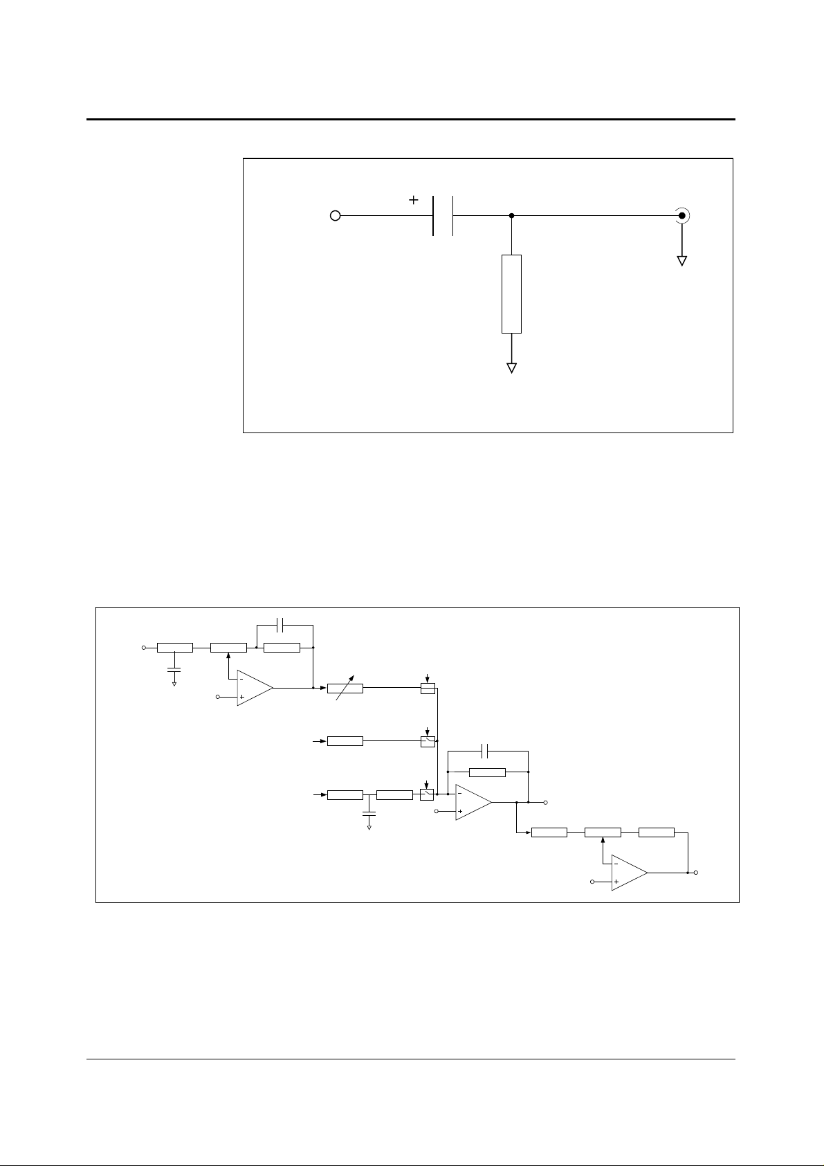
The recommended external components required to complete t he appl i cation are shown in Figure 21.
HPOUT
C1
R1
AGND
AGND
Figure 21 Headphone Output Application Drawing
Recommended values are C1 = 220uF (10V el ectrolytic), R1 = 47k
C1 forms a DC blocking capacitor to i solate the dc of the HPOUT f rom the headphones. R1 form a
pull down resistor to discharge C1 to prevent the voltage at the connec tion to the headphones from
rising to a level that m a y damage the headphones.
BYPASS MODE
The WM8731 includes a bypass mode whereby analogue line inputs are routed directly to the
analogue line outputs and headphone outputs. The scheme for this is i n Fi gure 22.
LINEIN
Figure 22 Signal Routing in Bypass Mode
12.5K
VMID
FROM
LINE
INPUTS
FROM
DAC
SIDETONE (OFF)
BYPASS (ON)
DACSEL (OFF)
VMID
LINEOUT
VMID
HPOUT
WOLFSON MICROELECTRONICS LTD AI Rev 2.0 February 2001
28
Page 29
WM8731 Advanced Information
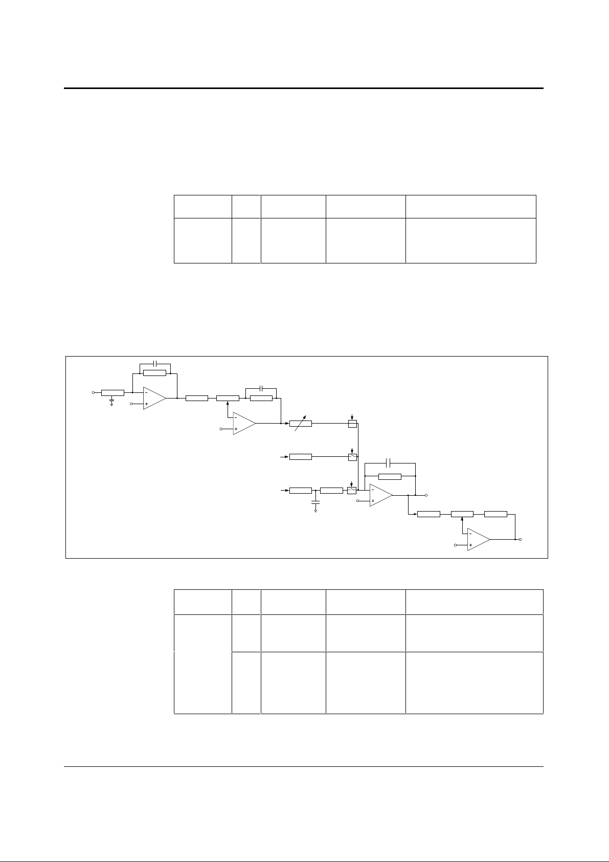
The bypass mode is selected under software control using the BYPASS mic rophone bit as shown in
Table 9. In true bypass mode, the output from the DA C (DACSEL) and (SIDETONE) shoul d be deselected from the l ine output block. However this can also be used to sum the DAC output, Line
Inputs together and microphone inputs. The analogue line input and headphone output volume
controls and mutes are still operational in bypass mode. The 0dB gain setting is rec ommended for
the Line Input volume control to avoid distortion. The m aximum s ignal at any point in the bypas s path
must be no greater than 1.0V rm s at AVDD = 3.3V , to avoid distort ion. This amplit ude tracks linearly
with AVDD. This means t hat if the DAC is producing a 1Vrm s signal, and it is being sum med with
1Vrms line BYPASS signal, the resulting LINEOP si gnal will be clipped.
MICIN
REGISTER
BIT LABEL DEFAULT DESCRIPTION
ADDRESS
0000100
Analogue
Audio Path
3 BYPASS 1 Bypass Switch (Analogue)
1 = Enable Bypass
0 = Disable Bypass
Control
Table 9 Bypass Mode Software Control
SIDETONE MODE
The WM8731 also includes a side tone mode where the microphone input is routed to line and
headphone outputs. The scheme for this is shown in Figure 23.
The side tone mode allows the microphone input to be att enuated to the outputs for telephone and
headset applications.
50k
10k
VMID
10dB GAIN BOOST
VMID
FROM
LINE
INPUTS
FROM
DAC
SIDETONE (ON)
BYPASS (OFF)
DACSEL (OFF)
LINEOUT
VMID
VMID
HPOUT
Figure 23 Side Tone Mode Schematic
REGISTER
BIT LABEL DEFAULT DESCRIPTION
ADDRESS
0000100
Analogue
Audio Path
Control
5 SIDETONE 0 Side Tone Switch (Analogue)
1 = Enable Side Tone
0 = Disable Side Tone
7:6 SIDEATT[1:0] 00 Side Tone Attenuation
11 = -15dB
10 = -12dB
01 = -9dB
00 = -6dB
Table 10 Side Tone Mode Table
WOLFSON MICROELECTRONICS LTD AI Rev 2.0 February 2001
29
Page 30

WM8731 Advanced Information
The side tone mode and attenuation i s selected under soft ware control using the SI DETONE bit as
shown in Table 10. In true side tone the output from the DAC (DACSEL) and line inputs (BYPASS)
should be deselected from the line output block. However, this can al so be used to sum the DAC
output, line inputs and microphone inputs together. The microphone boost gain control and
headphone output volume control and mutes are still operational in side tone m ode. The m aximum
signal at any point in the side tone path must be no greater than 1.0V rm s at VDD = 3.3V, to avoid
distortion. This am pl i tude tracks linearly with AVDD.
DEVICE OPERATION
DEVICE RESETTING
The WM8731 contains a power on reset circuit that resets the internal s tate of the device t o a known
condition. The power on reset is applied as DCVDD powers on and released only af ter the voltage
level of DCVDD crosses a m i nim um t urn off thres hold. If DCVDD lat er fal ls bel ow a m i nim um turn on
threshold voltage then the power on reset is re-applied. The threshold voltages and associated
hysteresis are shown in the Elec trical Characteristics table.
The user also has the ability to reset the device t o a known state under s oftware control as shown in
the table below.
REGISTER
ADDRESS
0001111
Reset Register
Table 11 Software Control of Reset
When using the software reset. In 3-wire mode the reset is applied on the rising edge of CSB and
released on the next rising edge of SCLK. I n 2-wire mode the reset is appli ed for the duration of the
ACK signal (approximately 1 SCLK peri od, refer to Figure 32).
BIT LABEL DEFAULT DESCRIPTION
8:0 RESET not reset Reset Register
Writing 00000000 to register resets
device
CLOCKING SCHEMES
In a typical digital audio system there is only one central c lock source produc ing a reference c lock to
which all audio data processing is synchroni sed. This cloc k is oft en ref erred to as t he audi o s yst em ’s
Master Clock. To allow WM8731 to be used in a c entral ly cloc k ed syst em , t he WM8731 is capable of
either generating this system c lock itself or receiving it from an external source as will be discus sed.
For applications where it is desirable that the WM8731 is the system clock source, then clock
generation is achieved through the use of a s uitable crystal c onnected between the XTI/MCLK input
and XTO output pins (see CRYSTAL OSCILLA TOR section).
For applications where a component other than the WM8731 will generate the reference cloc k, the
external system can be applied directly through the XTI/MCLK input pin with no software
configuration necessary. Note that in this sit uation, the osc illator c ircuit of the WM8731 can be saf ely
powered down to conserve power (see POWER DOWN section).
CORE CLOCK
The WM8731 DSP core can be c locked either by MCLK or MCLK di vided by 2. Thi s is controlled by
software as shown in Table 12 below.
REGISTER
ADDRESS
0001000
Sampling
Control
Table 12 Software Control of Core Clock
Having a programmable MCLK divider allows the device to be used in applications where higher
frequency master Clocks are available. For example the device can support 512fs master clocks
whilst fundamentally operating i n a 256f s mode.
WOLFSON MICROELECTRONICS LTD AI Rev 2.0 February 2001
BIT LABEL DEFAULT DESCRIPTION
6 CLKIDIV2 0 Core Cloc k divider select
1 = Core Clock is MCLK divided by 2
0 = Core Clock is MCLK
30
Page 31
WM8731 Advanced Information
CRYSTAL OSCILLATOR
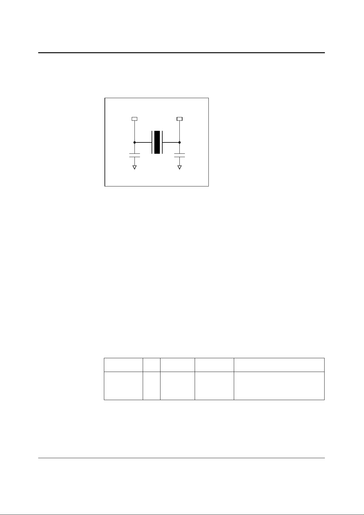
The WM8731 includes a crystal os cillator ci rcuit that allows the audio system ’s referenc e clock t o be
generated on the device. This is available to the rest of the audio system in buffered form on
CLKOUT. The crystal oscillator is a low radiation type, designed for low EMI. A typical application
circuit is shown in Figure 24.
XTI/MCLK XTO
Cp Cp
DGND DGND
Figure 24 Crystal Oscillator Application Circuit
For crystal frequencies in t he 12MHz range, a Cp of 10pF is recomm ended. For crys tal frequencies
in the 18MHz range, 15pF Cp is recommended.
The WM8731 crystal oscillator provides an extremely low jitter clock source. Low jitter clocks are a
requirement for high quality audio ADC and DACs, regardless of the converter architecture. The
WM8731 architecture is les s s usc eptible than m os t c onverter tec hniques but st ill requires c locks with
less than approximately 1ns of jitter to maintain performance. In applications where there is more
than one source for the mas ter cloc k, it is rec omm ended that t he clock is generated by t he W M8731
to minimise such problems.
CLOCKOUT
The Core Clock is internally buffered and made available externally to the audio system on the
CLKOUT output pin. CLKOUT provides a replicat ion of the Core Clock, but buff ered as suitable for
driving external loads.
There is no phase inversion between XTI/MCLK, the Core Clock and CLOCKOUT but there will
inevitably be some delay. The delay will be dependent on the load that CLOCKOUT drives. Refer to
Electrical Characteri stics.
CLKOUT can also be divided by 2 under software control, refer to Table 13. Note that if CLKOUT is
not required then the CLKOUT buffer on the W M8731 can be safely powered down to conserve
power (see POWER DOWN section). If the s yst em archi tec t has the c hoic e between using F
F
MCLK
or F
CLKOUT
= F
/2 in the interface, the l atter is recom mended t o conserve power. When the
MCLK
divide by two is selected CLKOUT changes on the rising edge of MCLK. Please ref er to Electrical
Characteristics for timing information.
REGISTER
BIT LABEL DEFAULT DESCRIPTION
ADDRESS
0001000
Sampling
Control
7 CLKODIV2 0 CLKOUT divider select
1 = CLOCKOUT is Core Clock
divided by 2
0 = CLOCKOUT is Core Clock
Table 13 Programming CLKOUT
CLKOUT is disabled and set low whenever the device is in reset.
CLKOUT
=
WOLFSON MICROELECTRONICS LTD AI Rev 2.0 February 2001
31
Page 32
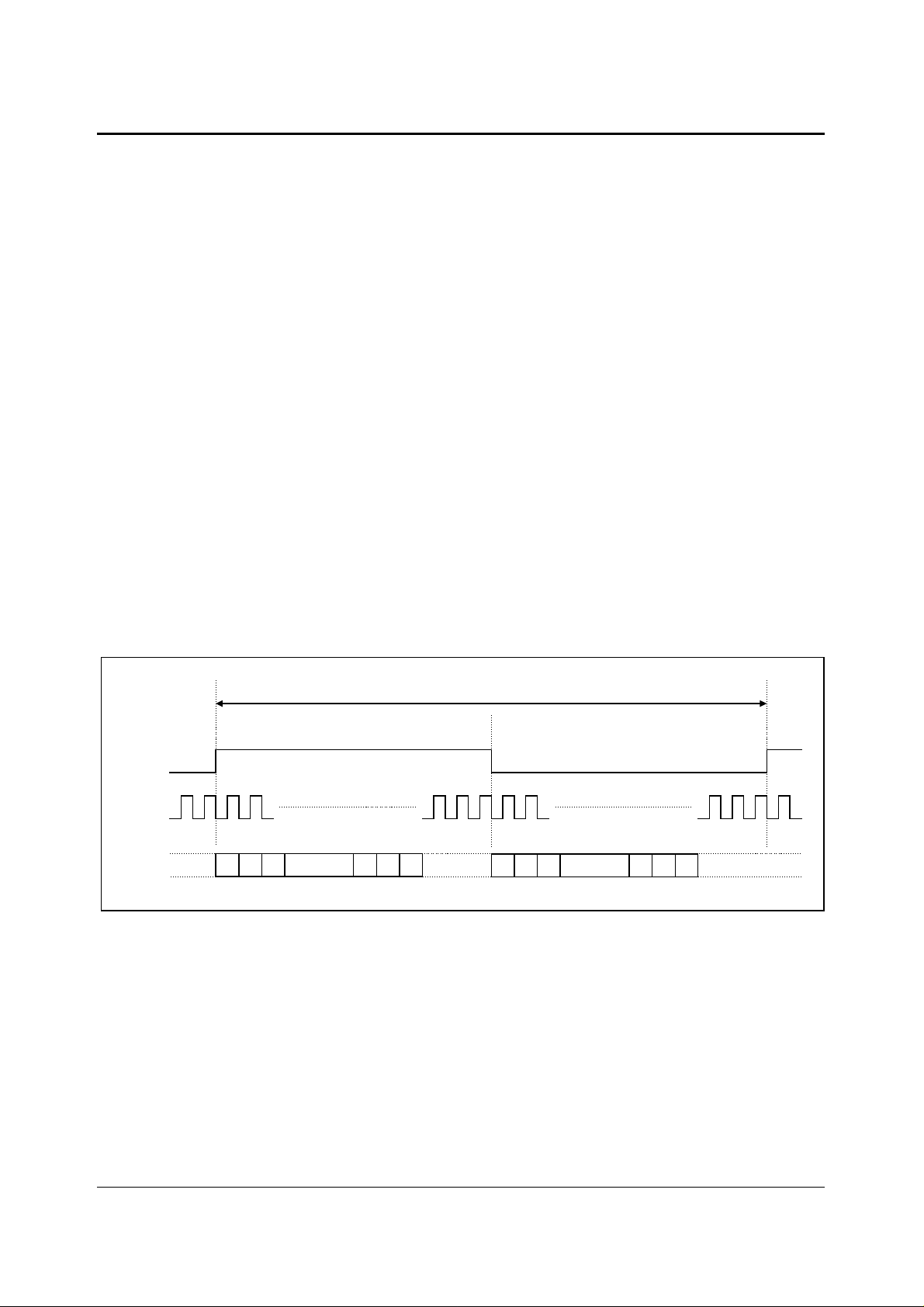
WM8731 Advanced Information
DIGITAL AUDIO INTERFACES
WM8731 may be operated in either one of the 4 offered audio interface modes. These are:
• Right justified
• Left justified
• I2S
• DSP mode
All four of these modes are MSB first and operate with data 16 to 32 bits.
Note that 32 bit data is not supported in right justified mode.
The digital audio interface tak es the data from the internal ADC digital filter and places it on the
ADCDAT output. ADCDAT is the form atted digital audio data stream output from t he ADC digital
filters with left and right channels m ultiplexed together. ADCLRC is an ali gnment clock t hat controls
whether Left or Right channel data is present on the ADCDAT lines. ADCDAT and ADCLRC are
synchronous with the BCLK signal with each data bit transition signified by a BCLK high to low
transition. BCLK m aybe an input or an output dependent on whether the devic e is in m ast er or s lave
mode. Refer to the MASTER/SLAVE OPERATION section
The digital audio interface als o receives the digital audio data for t he i nternal DAC digital filters on the
DACDAT input. DACDAT is t he formatted digital audio dat a stream output to the DAC di gital filters
with left and right channels multiplexed together. DACLRC is an alignment clock that controls
whether Left or Right channel data is pres ent on DACDA T. DA CDAT and DACLRC are synchronous
with the BCLK signal with each data bit t ransition signified by a BCLK high to l ow t ransition. DACDAT
is always an input. BCLK and DACLRC are either outputs or input s depending whether the device i s
in master or slave mode. Refer to the MASTER/SLAVE OPERATION section
DACLRC/
ADCLRC
BCLK
DACDAT/
ADCDAT
Figure 25 Left Justified Mode
There are four digital audio interface formats acc ommodated by the W M8731. These are shown in
the figures below. Refer to the Electrical Characteristi c section for timing information.
Left Justified mode i s where the MSB i s avail able on t he firs t ri sing edge of BCLK foll owing a ADCLR
or DACLRC transition.
1/fs
LEFT CHANNEL RIGHT CHANNEL
n-2 n-1
n321
LSBMSB
n-2 n-1
n321
LSBMSB
I2S mode is where the MSB is available on the 2nd rising edge of BCLK following a LRCLK
transition.
WOLFSON MICROELECTRONICS LTD AI Rev 2.0 February 2001
32
Page 33
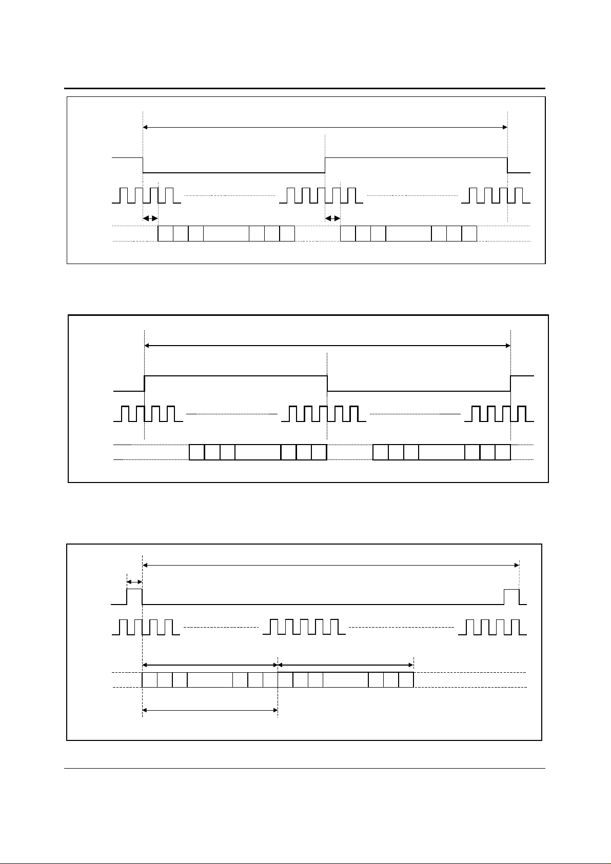
WM8731 Advanced Information
1/fs
LEFT CHANNEL RIGHT CHANNEL
DACLRC/
ADCLRC
BCLK
DACDAT/
ADCDAT
1 BCLK
MSB
Figure 26 I2S Mode
Right Justified mode is where the LSB is available on the ris ing edge of BCLK preceding a LRCLK
transition, yet MSB is still transmitted first.
DACLRC/
ADCLRC
BCLK
DACDAT/
ADCDAT
Figure 27 Right Justified Mode
DSP mode is where the left c hannel MSB is available on either the 1
(selectable by LRP) following a LRC transition high. Right channel data immediately follows left
channel data.
1 BCLK
n-2 n-1
LEFT CHANNEL RIGHT CHANNEL
n321
LSB
n-2 n-1
n-2 n-1
MSB
1/fs
n321
LSBMSB
st
n321
LSB
n-2 n-1
n321
LSBMSB
or 2nd rising edge of BCLK
1/fs
1 BCLK
DACLRC/
ADCLRC
BCLK
RIGHT CHANNEL
n-2 n-1
n321
DACDAT/
ADCDAT
LEFT CHANNEL
n-2 n-1
n321
LSBMSB
Input Word Length (IWL)
Note: Input word length is defined by the IWL register, LRP = 1
Figure 28 DSP Mode
WOLFSON MICROELECTRONICS LTD AI Rev 2.0 February 2001
33
Page 34

WM8731 Advanced Information
In all modes DACLRC and ADCLRC mus t always change on the falling edge of BCLK, refer to Figure
25, Figure 26, Figure 27 and Figure 28.
Operating the digital audio interface in DSP mode allows ease of use for supporting the various
sample rates and word lengths. The only requirem ent is t hat all data i s trans ferred within the c orrect
number of BCLK cycles to suit the chosen word length.
In order for the digital audio interface to offer similar support i n the three other m odes (Left Jus tified,
I2S and Right Justif ied), the DACLRC, ADCLRC and BCLK f requencies, continuit y and mark-spac e
ratios need more careful c onsideration.
In Slave mode, DACLRC and ADCLRC inputs are not required t o have a 50:50 mark-space ratio.
BCLK input need not be continuous. It is however required that t here are suffic ient BCLK cycles for
each DACLRC/ADCLRC transition t o cloc k the chos en data word length. The non-50: 50 requirem ent
on the LRCs is of use in some situations such as with a USB 12MHZ clock. Here simply dividing
down a 12MHz clock within the DSP to generate LRCs and BCLK will not generat e the appropriate
DACLRC or ADCLRC since they will no longer change on the falling edge of BCLK. For example,
with 12MHz/32k fs mode there are 375 MCLK per LRC. In these sit uations DACLRC/ADCLRC c an
be made non 50:50.
In Master mode, DACLRC and ADCLRC will be output with a 50:50 mark-s pace ratio with BCLK
output at 64fs. The exception again is in USB mode where BCLK is always 12MHz. So f or example in
12MHz/32k fs mode there are 375 m aster clocks per LRC period. Therefore DACLRC and ADCLRC
outputs will have a mark space ratio of 187: 188.
The ADC and DAC digital audio interfac e modes are sof tware configurable as indicated in Table 13.
Note that dynamically changing the software format may result in erroneous operation of the
interfaces and is theref ore not recommended.
The length of the digital audio data is programmable at 16/20/24 or 32 bi ts. Refer to the software
control table below. The data is s igned 2’s compl ement. Both ADC and DAC are f ixed at the same
data length. The ADC and DAC digital filters process data us i ng 24 bi ts. If the ADC is programmed to
output 16 or 20 bit data then it st rips the LSBs from the 24 bit data. If the ADC is programmed to
output 32 bits then it packs the LSBs with zeros. If the DAC is programmed to receive 16 or 20 bit
data, the WM8731 packs the LSBs with zeros. If the DAC is programmed to receive 32 bit data, then
it strips the LSBs.
The DAC outputs can be swapped under software control using LRP and LRSWAP as shown in
Table 14. Stereo samples are normally generated as a Left/Right sampled pair. LRSW AP reverses
the order so that a Left sample goes to the right DAC output and a Right sample goes to the left DAC
output. LRP swaps the phasing so that a Right/Left sampled pair is expected and preserves the
correct channel phase diff erence.
To accommodate system timing requirements the interpretation of BCLK maybe inverted, this is
controlled vias the software shown in Table 14. This is especially appropriat e for DSP mode.
ADCDAT lines are always outputs. They power up and return from standby low.
DACDAT is always an input. It i s expected to be set low by the audio interface c ontroller when the
WM8731 is powered off or in st andby.
ADCLRC, DACLRC and BCLK can be either outputs or inputs depending on whether the devi ce is
configured as a mast er or slave. If the device i s a master then the DACLRC and BCLK signals are
outputs that default low. If the device is a slave then the DACLRC and BCLK are inputs. It is
expected that these are set low by the audio interfac e controll er when the W M8731 is powered off or
in standby.
WOLFSON MICROELECTRONICS LTD AI Rev 2.0 February 2001
34
Page 35

WM8731 Advanced Information
REGISTER
BIT LABEL DEFAULT DESCRIPTION
ADDRESS
0000111
1:0 FORMAT[1:0] 10 Audio Data Format S el ect
Digital Audio
Interface
Format
3:2 IWL[1:0] 10 Input Audio Data Bit Length Select
4 LRP 0 DACLRC phase control (in left, right
5 LRSWAP 0 DAC Left Right Clock Swap
6 MS 0 Master Slave Mode Control
7 BCLKINV 0 Bit Clock Invert
Table 14 Digital Audio Interface Control
11 = DSP Mode, frame sync + 2
data packed words
2
10 = I
S Format, MSB-First left-1
justified
01 = MSB-First, left justified
00 = MSB-First, right justified
11 = 32 bits
10 = 24 bits
01 = 20 bits
00 = 16 bits
or I2S modes)
1 = Right Channel DAC data when
DACLRC high
0 = Right Channel DAC data when
DACLRC low
(opposite phasing in I
2
S mode)
or
DSP mode A/B sel ect (in DSP mode
only)
1 = MSB is available on 2nd BCLK
rising edge after DACLRC rising
edge
0 = MSB is available on 1st BCLK
rising edge after DACLRC rising
edge
1 = Right Channel DAC Data Left
0 = Right Channel DAC Data Right
1 = Enable Master Mode
0 = Enable Slave Mode
1 = Invert BCLK
0 = Don’t invert BCLK
Note: If right justi fied 32 bit mode is selected then the WM8731 defaults to 24 bits.
MASTER AND SLAVE MODE OPERATION
The WM8731 can be configured as either a m aster or slave mode device. As a m aster mode device
the WM8731 controls sequencing of the data and clocks on the digital audio interface. As a slave
device the WM8731 responds with data to the clo cks it receives over the digital audio interface. The
mode is set with the MS bit of the control register as s hown in Table 15.
REGISTER
ADDRESS
0000111
Digital Audio Interfac e
Format
Table 15 Programming Master/Slave M odes
WOLFSON MICROELECTRONICS LTD AI Rev 2.0 February 2001
BIT LABEL DEFAULT DESCRIPTION
6 MS 0 Master Slave Mode Control
1 = Enable Master Mode
0 = Enable Slave Mode
35
Page 36
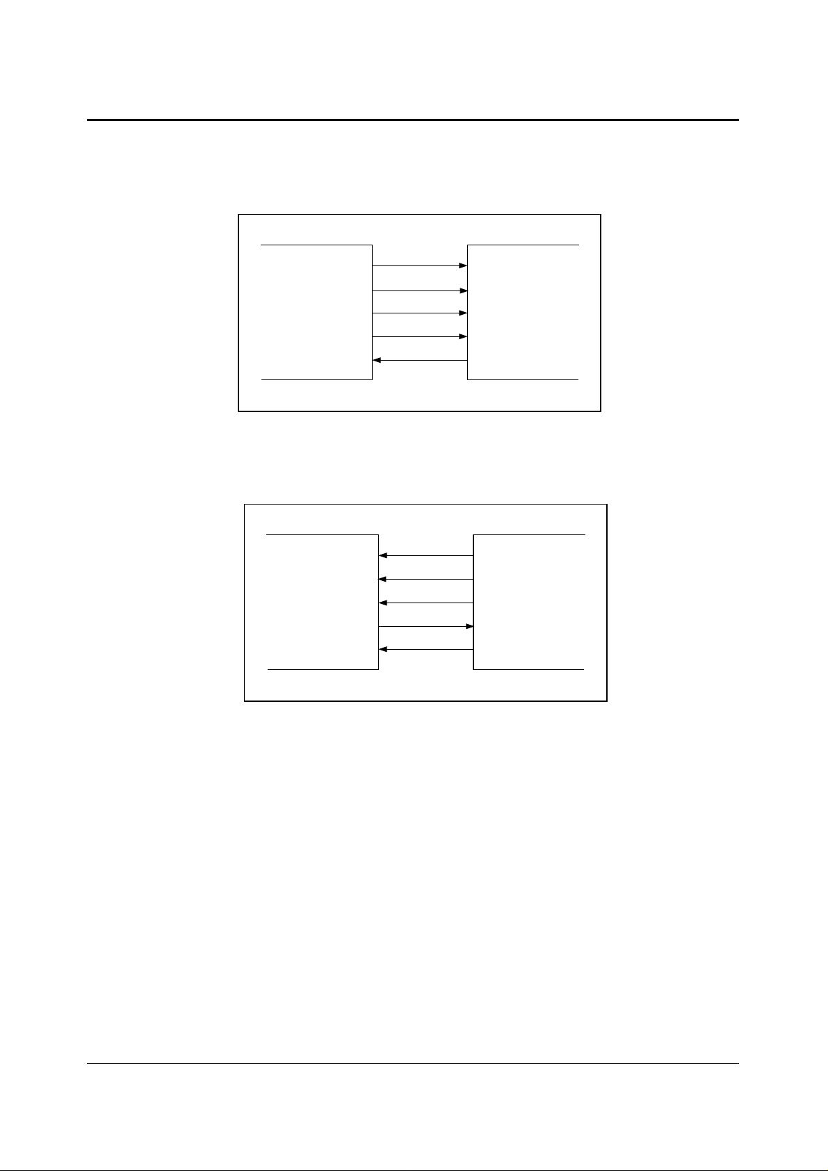
WM8731 Advanced Information
As a master mode device the WM8731 controls the sequencing of data transfer (ADCDAT,
DACDAT) and output of clocks (BCLK, ADCLRC, DACLRC) over the digital audio interface. It uses
the timing generated from eit her it s on-board c ryst al or the MCLK i nput as t he ref erence f or t he c loc k
and data transitions. This is illustrated in Figure 29. ADCDAT is always an output from and DACDAT
is always an input to the WM8731 independent of master or sl ave mode.
BCLK
ADCLRC
WM8731
CODEC
Note: ADC and DAC can run at different rates
Figure 29 Master Mode
As a slave device the W M8731 sequences the data transfer (ADCDAT, DACDA T) over the digital
audio interface in response to the external applied clocks (BCLK, ADCLRC, DACLRC). This is
illustrated in Figure 30.
WM8731
CODEC
Note: The ADC and DAC can run at different rates
DACLRC
ADCDAT
DACDAT
BCLK
ADCLRC
DACLRC
ADCDAT
DACDAT
DSP
ENCODER/
DECODER
DSP
ENCODER/
DECODER
Figure 30 Slave Mode
Note that the WM8731 relies on controlled phase relationships between audio interface BCLK,
DACLRC and the master MCLK or CLKOUT. To avoi d any ti m ing hazards , refer to t he t im i ng s ect ion
for detailed informati on.
AUDIO DATA SAMPLING RATES
The WM8731 provides for two modes of operation (normal and USB) to generat e the required DAC
and ADC sampling rates. Normal and USB m odes are program m ed under s oft ware control ac c ording
to the table below.
In Normal mode, the user controls the sample rate by using an appropriate MCLK or crystal
frequency and the sample rate control register setting. The WM8731 can support sample rates from
8ks/s up to 96ks/s.
In USB mode, the user m ust use a fixed MLCK or c rystal frequency of 12MHz to generate sam ple
rates from 8ks/ s to 96ks/s. It is called USB mode since the common USB (Universal Serial Bus)
clock is at 12MHz and the WM8731 can be directly used within such systems. WM8731 can
generate all the normal audio sample rates from thi s one Mast er Cloc k f requency, rem oving t he need
for different master clocks or PLL circuits.
WOLFSON MICROELECTRONICS LTD AI Rev 2.0 February 2001
36
Page 37

WM8731 Advanced Information
Uniquely, the WM8731 offers t he user the ability to sample the ADC and DAC at different rates under
software control in both Normal and USB modes. The reduces the burden on any cont rolling DSP.
However, the signal processing in t he ADC and DAC over-sam pling filters is tight ly coupled together
in order to minimis e power consumpt ion. To thi s end, only t he com binations of sam ple rates l isted in
the following sections are support ed. Note that t hese rates support ed are anti cipated t o be the likely
combinations used in typical audio systems .
REGISTER
ADDRESS
0001000
Sampling
Control
Table 16 Sample Rate Control
BIT LABEL DEFAULT DESCRIPTION
0 USB/
NORMAL
1 BOSR 0 Base Over-Sampling Rate
5:2 SR[3:0] 0000 ADC and DAC sample rate control;
0 Mode Select
1 = USB mode (250/272fs)
0 = Normal mode (256/384fs)
USB Mode
0 = 250fs
1 = 272fs
See USB Mode and Normal Mode
Sample Rate secti ons for operation
Normal Mode
0 = 256fs
1 = 384fs
NORMAL MODE SAMPLE RATES
In normal mode MCLK/crystal oscillat or is set up according to the desired s ample rates of the ADC
and DAC. For ADC or DAC sampling rates of 8, 32, 48 or 96kHz, MCLK frequencies of either
12.288MHz (256fs) or 18.432MHz (384fs) can be used. For A DC or DAC s am pling rat es of 8, 44. 1 or
88.2kHz from MCLK frequencies of either 11.2896MHz (256fs) or 16.9344MHz (384fs) can be used.
The table below should be used to set up the device to work with the various sample rate
combinations. For exampl e if the us er wishes to use t he W M8731 in norm al mode with the A DC and
DAC sample rates at 48k Hz and 48kHz respectively then the device s hould be programmed with
BOSR = 0, SR3 = 0, SR2 = 0, SR1 = 0 and SR0 = 0 with a 12.288MHz MCLK or with BOSR = 1,
SR3 = 0, SR2 = 0, SR1 = 0 and SR0 = 0 with a 18.432MHz MCLK. The ADC and DAC will then
operate with a Digital Filter of type 1, ref er to Digital Filt er Characteristics section f or an explanation
of the different filt er t ypes.
WOLFSON MICROELECTRONICS LTD AI Rev 2.0 February 2001
37
Page 38

WM8731 Advanced Information
SAMPLING
RATE
ADC DAC
kHz kHz MHz BOSR
(Note 1)
44.1
(Note 1)
(Note 1)8(Note 1)
Table 17 Normal Mode Sample Rate Look-up Table
MCLK
FREQUENCY
REGISTER SETTINGS
SR3 SR2 SR1 SR0
12.288 0 0 0 0 048 48
18.432 1 0 0 0 0
12.288 0 0 0 0 148 8
18.432 1 0 0 0 1
12.288 0 0 0 1 0848
18.432 1 0 0 1 0
12.288 0 0 0 1 188
18.432 1 0 0 1 1
12.288 0 0 1 1 032 32
18.432 1 0 1 1 0
12.288 0 0 1 1 196 96
18.432 1 0 1 1 1
11.2896 0 1 0 0 044.1 44.1
16.9344 1 1 0 0 0
11.2896 0 1 0 0 144.1 8
16.9344 1 1 0 0 1
11.2896 0 1 0 1 08
16.9344 1 1 0 1 0
11.2896 0 1 0 1 18
16.9344 1 1 0 1 1
11.2896 0 1 1 1 188.2 88.2
16.9344 1 1 1 1 1
SAMPLE
RATE
DIGITAL
FILTER
TYPE
1
1
1
1
1
2
1
1
1
1
2
Notes:
1. 8k not exact, actual = 8.018kHz
2. All other combinations of B OS R and SR[3:0] that are not in the truth table are invalid
The BOSR bit represents the bas e over-sampling rate. This is the rate that the WM8731 digital signal
processing is carried out at. In Normal mode, with B OSR = 0, the base over-sampling rat e is at
256fs, with BOSR = 1, the base over-s ampling rate is at 384fs. This can be used to determine the
actual audio data rate produced by the A DC and requi red by the DAC.
Example scenarios are:
1. with a requirement that the ADC data rate is 8kHz and DAC dat a rate is 48kHz, then choosing
MCLK = 12.288MHz the device is programm ed with BOSR = 0 (256fs ), SR3 = 0, SR2 = 0, S R1
= 1, SR0 = 0.The ADC output data rate will then be exactly 8kHz (derived from 12.288MHz/256
x1/6) and the DAC expects data at exactly 48kHz (derived from 12.288MHz/256)
2. with a requirement that ADC data rat e is 8kHz and DAC data rate is 44.1kHz, then choosing
MCLK = 16.9344MHz the device is programm ed with B OSR = 1 (384fs), SR3 = 1, SR2 = 0, SR1
= 0, SR0 = 1. The ADC will no longer output data at exactly 8.000kHz, instead it will be
8.018kHz (derived from 16.9344MHz/384 x 2/11), the DAC still is at exactly 44. 1kHz (derived
from 16.9344MHz/384). A slight (sub 0. 5%) pitch shift will therefore result in t he 8kHz audio
data and (importantly) the user m us t ens ure that the dat a acros s t he di git al interf ace is correc tl y
synchronised at the 8.018kHz rat e.
WOLFSON MICROELECTRONICS LTD AI Rev 2.0 February 2001
38
Page 39
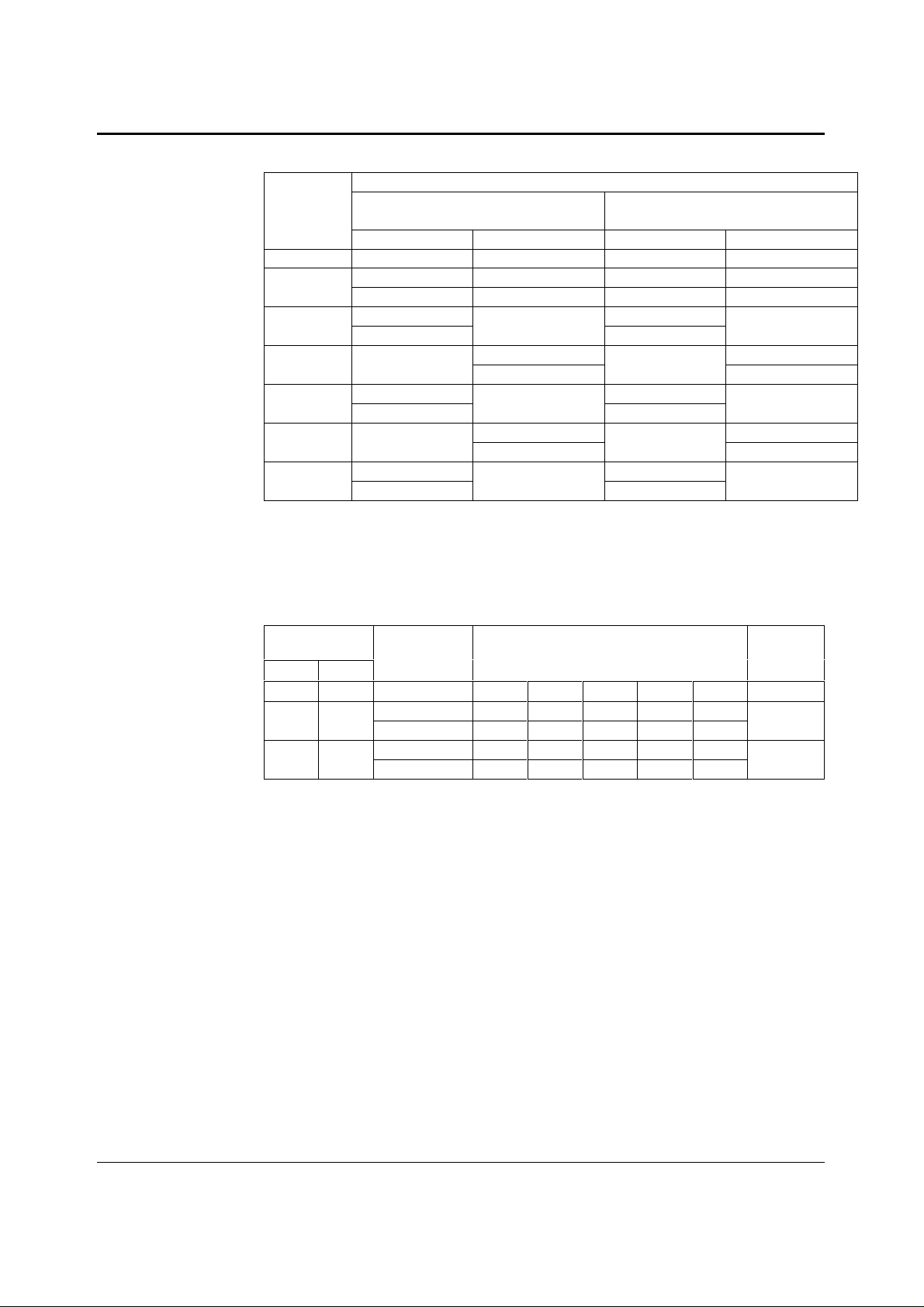
WM8731 Advanced Information
The exact sample rates achieved are def i ned by the relationships in Table 18 below.
TARGET
SAMPLING
RATE
BOSR=0
(256fs)
ACTUAL SAMPLING RATE
BOSR=1
(384fs)
MCLK=12.288 MCLK=11.2896 MCLK=18.432 MCLK=16.9344
kHz kHz kHz kHz kHz
8
32
44.1
48
88.2
96
8 8.018 8 8.018
12.288MHz/256 x 1/6 11.2896MHz/256 x 2/11 18.432MHz/384 x 1/6 16.9344MHz/384 x 2/11
32 32
12.288MHz/256 x 2/3
not available
48 48
12.288MHz/256
not available
96 96
12.288MHz/256 x 2
not available
18.432MHz/384x 2/3
44.1 44.1
11.2896MHz/256
not available
not available
18.432MHz/384
88.2 88.2
11.2896MHz/384 x 2
not available
not available
18.432MHz/384 x 2
not available
16.9344MHz /384
not available
16.9344MHz /384 x 2
not available
Table 18 Normal Mode Actual Sample Rates
128/192fs NORMAL MODE
The Normal Mode sample rates are designed for standard 256fs and 384fs MCLK rates. However the
WM8731 is also capabl e of being clocked from a 128 or 192fs MCLK for applic ation over limited
sampling rates as s hown in the table below.
SAMPLING
RATE
ADC DAC
kHz kHz MHz BOSR
MCLK
FREQUENCY
6.144 0 0 1 1 148 48
SAMPLE
RATE
REGISTER SETTINGS
SR3 SR2 SR1 SR0
DIGITAL
FILTER
TYPE
2
9.216 1 0 1 1 1
5.6448 0 1 1 1 144.1 44.1
2
8.4672 1 1 1 1 1
Table 19 128fs Normal Mode Sample Rate Look-up Table
512/768fs NORMAL MODE
512 fs and 768 fs MCLK rates can be ac comm odated by using the CLKI DIV2 bit. The core c lock t o
the DSP will be divided by 2 so an external 512/768 MCLK will become 256/384 fs internally and the
device otherwise operates as in Table 15 but with MCLK at t wice the specified rate. See Table 12 for
software control.
WOLFSON MICROELECTRONICS LTD AI Rev 2.0 February 2001
39
Page 40

WM8731 Advanced Information
USB MODE SAMPLE RATES
In USB mode the MCLK/crystal oscillator input is 12MHz only.
SAMPLING
RATE
ADC DAC
kHz kHz MHz BOSR
48 48 12.000 0 0 0 0 0 0
44.1
(Note 2)
48 8 12.000 0 0 0 0 1 0
44.1
(Note 2)
8 48 12.000 0 0 0 1 0 0
8
(Note 1)
8 8 12.000 0 0 0 1 1 0
8
(Note 1)8(Note 1)
32 32 12.000 0 0 1 1 0 0
96 96 12.000 0 0 1 1 1 3
88.2
(Note 3)
Table 20 USB Mode Sample Rate Look-up Table
44.1
(Note 2)
8
(Note 1)
44.1
(Note 2)
88.2
(Note 3)
MCLK
FREQUENCY
12.000 1 1 0 0 0 1
12.000 1 1 0 0 1 1
12.000 1 1 0 1 0 1
12.000 1 1 0 1 1 1
12.000 1 1 1 1 1 2
SAMPLE
RATE
REGISTER SETTINGS
SR3 SR2 SR1 SR0
DIGITAL
FILTER
TYPE
Notes:
1. 8k not exact, actual = 8.021kHz
2. 44.1k not exact, actual = 44.118kHz
3. 88.1k not exact, actual = 88.235kHz
4. All other combinations of B OS R and SR[3:0] that are not in the truth table are invalid
The table above can be used to set up the device to work with various sample rate combi nations . For
example if the user wishes to use the WM8731 in USB mode with the A DC and DAC s am ple rat es at
48kHz and 48kHz respectively then the device should be programm ed with BOS R = 0, SR3 = 0, SR2
= 0, SR1 = 0 and SR0 = 0. The ADC and DAC will then operate with a Digital Filter of type 0, ref er t o
Digital Filter Characteris tics section for an explanation of the different filter types.
The BOSR bit represents the bas e over-sampling rate. This is the rate that the WM8731 digital signal
processing is carried out at and the sam pling rate will always be a sub-multiple of this . In US B m ode,
with BOSR = 0, the base over-sampl ing rate is defined at 250fs, with BOSR = 1, the base oversampling rate is defined at 272fs. This can be used to determine the actual audio sampling rate
produced by the ADC and required by the DAC.
Example scenarios are, :-
1. with a requirem ent that the ADC data sampling rate is 8k Hz and DAC data sampling rate is
48kHz the device is programmed with BOSR = 0 (250fs), SR3 = 0, SR2 = 0, SR1 = 1, SR0 =
0.The ADC will then be exactly 8kHz ( derived from 12MHz/250 x 1/6 ) and the DAC expects
data at exactly 48kHz ( derived from 12MHz/250 ).
2. with a requirement that ADC data rate is 8kHz and DAC data rate is 44.1kHz the device is
programmed with BOSR = 0 (272fs), SR3 = 0, SR2 = 0, SR1 = 1, SR0 = 0. The ADC will not
output data at exactly 8kHz, instead it will be 8.021k Hz ( derived from 12MHz/272 x 2/11 ) and
the DAC at 44.118kHz ( derived from 12MHz/272 ). A slight (sub 0. 5%) pitch s hift will therefore
results in the 8kHz and 44.1k Hz audio data and (more important ly) the user must ensure that
the data across the digital interf ace is correctly synchronised at the 8. 021kHz and 44.117kHz
rates.
WOLFSON MICROELECTRONICS LTD AI Rev 2.0 February 2001
40
Page 41

WM8731 Advanced Information
The exact sample rates supported f or all combinations are defi ned by the relationships in Table 21
below.
TARGET
SAMPLING
RATE
ACTUAL SAMPLING RATE
BOSR=0
( 250fs)
kHz kHz kHz
8 8.0218
12MHz/(250 x 48/8) 12MHz/(272 x 11/2)
3232
12MHz/(250 x 48/32)
4848
12MHz/250
9696
12MHz/125
Table 21 USB Mode Actual Sample Rates
ACTIVATING DSP AND DIGITAL AUDIO INTERFACE
To prevent any communication problems from arising across the Digital A udio Interface the Audio
Interface is disabled (tris tate with weak 100k pulldown). Once t he Audio Interf ace and the Sam pling
Control has been programmed it i s activated by setting t he A CTI VE bit under Software Control.
REGISTER
ADDRESS
0001001
Active Control
Table 22 Activating DSP and Digital Audio Interface
BIT LABEL DEFAULT DESCRIPTION
0 ACTIVE 0 Activate Interface
BOSR=1
(272fs)
not available
44.11744.1 not available
12MHz/272
not available
88.23588.2 not available
12MHz/136
not available
1 = Active
0 = Inactive
It is recomm ended that bet ween changing any content of Digital Audio Interf ace or Sam pling Control
Register that the acti ve bi t i s reset then set.
SOFTWARE CONTROL INTERFACE
The software control interface m ay be operat ed usi ng either a 3-wire (SP I-c om pati ble) or 2-wire MPU
interface. Select i on of i n t erface format is ac hi eved by setting the state of t he MODE pin.
In 3-wire mode, SDIN is used for t he program data, SCLK i s used to cloc k in the program data and
CSB is used to latc h in the program data. In 2-wire mode, SDIN is used for serial data and SCLK is
used for the serial clock. In 2-wire m ode, the state of CSB pin al lows the user to select one of two
addresses.
SELECTION OF SERIAL CONTROL MODE
The serial control interfac e may be selec ted to operate in eit her 2 or 3-wire modes. This is achieved
by setting the state of the MODE pin.
MODE INTERFACE
02 wire
13 wire
Table 23 Control Interface Mode Selection
WOLFSON MICROELECTRONICS LTD AI Rev 2.0 February 2001
FORMAT
41
Page 42
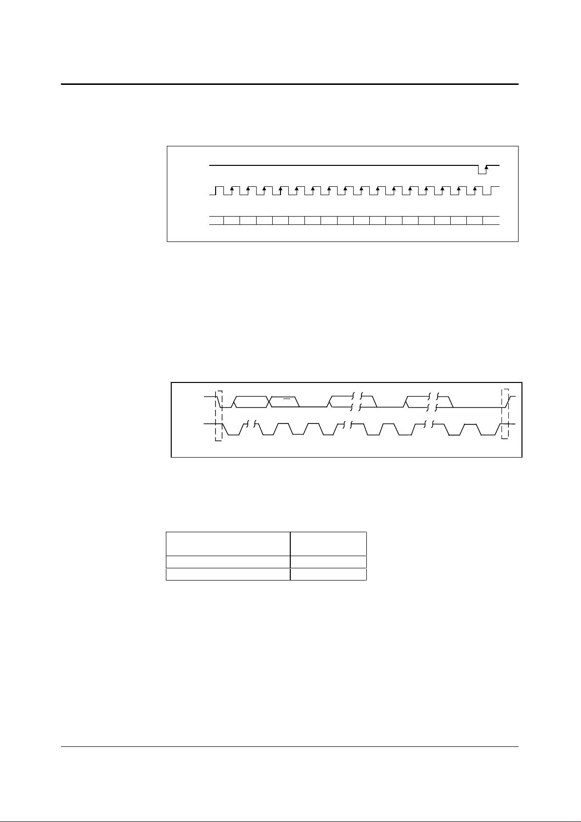
WM8731 Advanced Information
3-WIRE (SPI COMPATIBLE) SERIAL CONTROL MODE
The WM8731 can be controlled using a 3-wire serial interface. SDIN i s used for the program data,
SCLK is used to clock in the program data and CSB is use t o latch in the program data. The 3-wire
interface protocol is s hown in Figure 31.
CSB
SCLK
SDIN
B15 B6B7B8B9B10B11B12B13B14 B1B2B3B4B5 B0
Figure 31 3-Wire Serial Interface
Notes:
1. B[15:9] are Control Address B i ts
2. B[8:0] are Control Data Bit s
3. CSB is edge sensitive not l evel sensitive. The data is latched on the rising edge of CSB.
2-WIRE SERIAL CONTROL MODE
The WM8731 supports a 2-wire MPU serial interface. The device operates as a slave device only.
The WM8731 has one of two slave addresses that are selected by setting the state of pin 10, (CSB).
SDIN
R ADDR
SCLK
START
Figure 32 2-Wire Serial Interface
Notes:
ACK
DATA B15-8
ACK
DATA B7-0R/W
ACK
STOP
1. B[15:9] are Control Address Bits
2. B[8:0] are Control Data Bits
CSB STATE
Address
(Default = LOW)
0 0011010
1 0011011
Table 24 2-Wire MPU Interface Address Selection
WOLFSON MICROELECTRONICS LTD AI Rev 2.0 February 2001
42
Page 43

WM8731 Advanced Information
To control the WM8731 on the 2-wire bus the master control devi ce must initi ate a data transfer by
establishing a start c ondition, defined by a high t o low transition on SDIN while SCLK remains hi gh.
This indicates that an address and data t ransfer will follow. All peripherals on the 2-wire bus respond
to the start condition and s hift in the next eight bits (7-bit address + R/W bit ). The trans fer is MSB
first. The 7-bit address consists of a 6-bit base address + a single programm able bit to s elect one of
two available addresses for this devi ce (see table 24). If the correct address i s received and the R/ W
bit is ‘0’, indicating a write, then the WM8731 will respond by pulling SDIN low on the next clock puls e
(ACK). The WM8731 is a write only device and will only respond to the R/W bit indicati ng a write. If
the address is not recognised the device will return to the idle condition and wait for a new start
condition and valid address.
Once the WM8731 has ack nowledged a correct address, t he controller will send eight data bits (bits
B[15]-B[8]). W M8731 will then acknowledge the sent data by pulling SDIN low for one c lock pulse.
The controller will then send the remaining eight data bits (bit s B[7]-B[0]) and the W M8731 will then
acknowledge again by pulling SDIN low.
A stop condition is defined when there is a low to high transiti on on SDIN while SCLK is high. If a
start or stop condition is detected out of sequence at any point in the data trans fer then the device
will jump to the idle condition.
After receiving a complete addres s and data sequence the WM8731 returns to the idle s tate and
waits for another start condit ion. Each write to a register requires the com plete sequence of start
condition, device address and R/W bit foll owed by the 16 register address and data bits.
POWER DOWN MODES
The WM8731 contains power conservation modes in which various circuit blocks may be safely
powered down in order to conserve power. This is software programm able as shown in the table
below.
REGISTER
ADDRESS
0000110
Power Down
Control
Table 25 Power Conservation Modes Software Control
BIT LABEL DEFAULT DESCRIPTION
0 LINEINPD 1 Li ne Input Power Down
1 MICPD 1 Microphone Input an Bias
2 ADCPD 1 ADC Power Down
3 DACPD 1 DAC Power Down
4 OUTPD 1 Line Output Power Down
5 OSCPD 0 Oscillator Power Down
6 CLKOUTPD 0 CLKOUT power down
7 POWEROFF 1 Power Off Device
1 = Enable Power Down
0 = Disable Power Down
Power Down
1 = Enable Power Down
0 = Disable Power Down
1 = Enable Power Down
0 = Disable Power Down
1 = Enable Power Down
0 = Disable Power Down
1 = Enable Power Down
0 = Disable Power Down
1 = Enable Power Down
0 = Disable Power Down
1 = Enable Power Down
0 = Disable Power Down
1 = Device Power Off
0 = Device Power On
WOLFSON MICROELECTRONICS LTD AI Rev 2.0 February 2001
43
Page 44

WM8731 Advanced Information
The power down control can be used to either a) permanent ly dis able func tions when not required in
certain applications or b) to dynamical ly power up and down functions depending on the operating
mode, e.g.: during playback or record. Please follow the special instructions below if dynamic
implementations are being used.
LINEINPD: Simultaneously powers down both the Line Inputs. Thi s can be done dynami cally without
any audible effects either on t he ADC or to the Line Outputs in Bypass mode. This is of use when t he
device enters Playback, Pause or Stop modes or the Microphone i nput has been selected.
MICPD: Simultaneously powers down both the Microphone Input and Microphone Bias. If this is done
dynamically, audible pops through the ADC will result. This will only be audible if the Microphone
Input is selected to the A DC at the time. If the state of MICPD is changed then the controlling DSP or
microprocessor s hould switch t o select the Line Input s as input to t he ADC (INSEL) before changing
MICPD. This is of use when the devic e enters Playback, Pause or Stop m odes or the Microphone
Input is not selected.
ADCPD: Powers down the ADC and ADC Filters. If this is done dynamically then audible pops will
result if any signals were present through the ADC. To overcome this whenever the ADC is to be
powered down, either mute the Microphone Input (MUTEIN) or MUTELINE IN, then c hange ADCPD.
This is of use when the device enters Playback, Pause or Stop modes regardless of whether
Microphone or Line Inputs are selected.
DACPD: Powers down the DAC and DAC Digital Filters. If this is done dynamically then audible pops
will result unless the following guidelines are followed. In order to prevent pops, the DAC should first
be soft-muted (DACMU), the out put should then be de-selected from the line and headphone output
(DACSEL), then the DAC powered down (DACPD). This is of use when the device enters Record,
Pause, Stop or Bypass modes.
OUTPD: Powers down the Line Headphone Output. If this is done dynam ically then audible pops
may result unless the DAC is first soft-muted (DACMU). This is of use when the device enters
Record, Pause or Stop modes.
OSCPD: Powers off the on board crystal oscillator. The MCLK input will function independently of the
Oscillator being powered down.
CLKOUTPD: Powers down the CLOCKOUT pin. This cons erves power, reduces digital noise and RF
emissions if not required. CLKOUT is tied low when powered down.
The device can be put into a standby mode (STANDBY) by powering down all the audio ci rcuitry
under software control as shown in Table 18. If the cryst al osc illator and/or CLOK OUT pins are being
used to derive the system master clock, these should probably never be powered off in standby.
Provision has been made to independent l y power off these areas according to Table 26.
DESCRIPTION
POWER OFF
CLKOUTPD
OSCPD
0001111 1
0101111 1
0111111 1
Table 26 Standby Mode
DACPD
ADCPD
MICPD
OUTPD
LINEINPD
STANDBY, but with Crystal
Oscillator OS and CLKOUT
available
STANDBY, but with Crystal
Oscillator OS available,
CLKOUT not-available
STANDBY, Crystal
oscillator and CLKOUT notavailable.
In STANDBY mode the Cont rol Interface, a small portion of t he digital and areas of the analogue
circuitry remain active. The active analogue includes the analogue VMID reference so that the
analogue line inputs, line output s and headphone outputs remai n biased to VMID. This reduc es any
audible effects caused by DC glitches when entering or leaving STANDB Y mode.
The device can be powered off by writing to the POWEROFF bit of the Power Down register. In
POWEROFF mode the Control Interface and a small portion of the digital remain active. The
WOLFSON MICROELECTRONICS LTD AI Rev 2.0 February 2001
44
Page 45
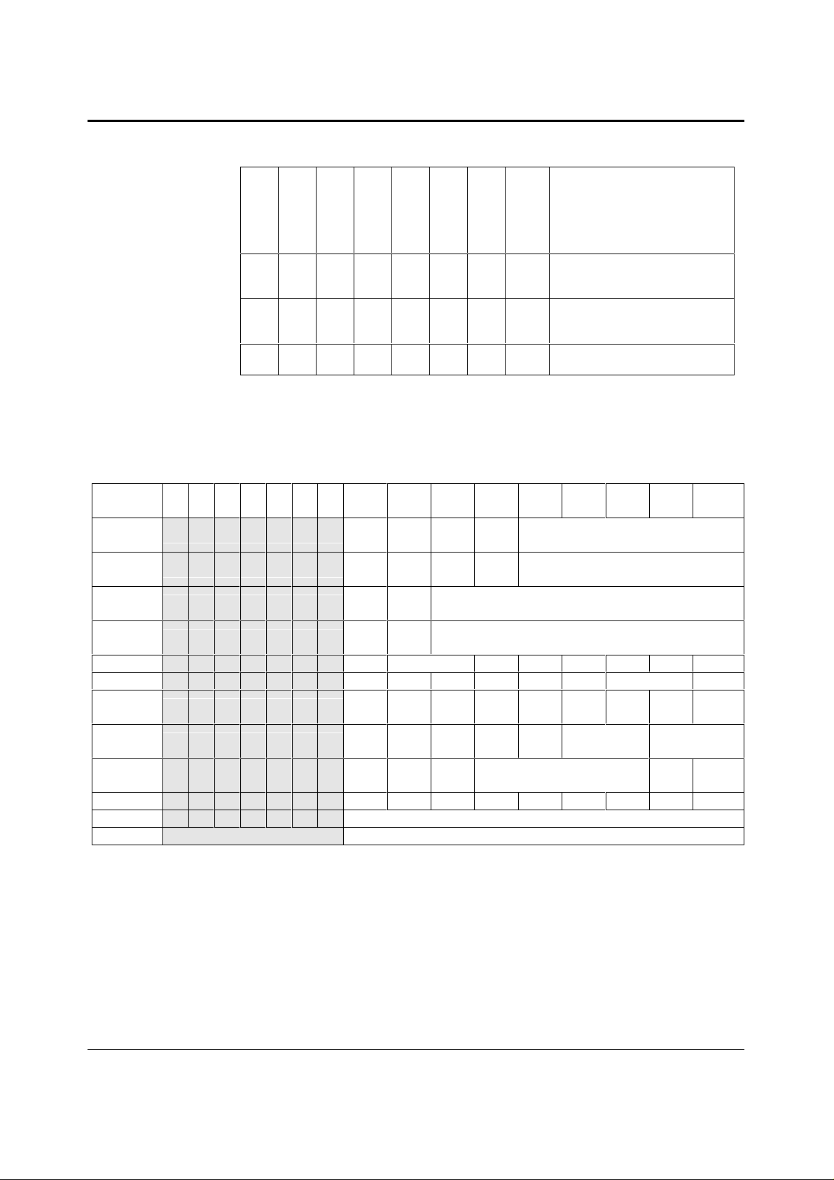
WM8731 Advanced Information
analogue VMID reference is disabled. As in STANDBY mode the crys tal oscillator and/or CLKOUT
pin can be independently controlled. Ref er to Table 27.
DESCRIPTION
POWER OFF
CLKOUTPD
OSCPD
OUTPD
DACPD
ADCPD
MICPD
LINEINPD
100X11XX
POWEROFF, but with Crystal
Oscillator OS and CLKOUT
available
110X11XX
POWEROFF, but with Crystal
Oscillator OS available, CLKOUT
not-available
111X11XX
POWEROFF, Crystal oscillator
and CLKOUT not-available.
Table 27 Poweroff Mode
REGISTER MAP
The complete register m ap is shown in Table 28. The detailed des cription can be found in Table 29
and in the relevant text of the device description. There are 11 registers with 16 bits per register (7 bi t
address + 9 bits of data). Thes e can be controlled using either the 2 wire or 3 wire MPU interface.
REGISTER B15B14B13B12B11B10B9B8 B7 B6 B5 B4 B3 B2 B1 B0
R0 (00h)
R1 (02h)
R2 (04h)
R3 (06h)
R4 (08h)
R5 (0Ah)
R6 (0Ch)
R7 (0Eh)
R8 (10h)
R9 (12h)
R15(1Eh)
0 0 0 0 0 0 0
0 0 0 0 0 0 1
0 0 0 0 0 1 0
0 0 0 0 0 1 1
0 0 0 0 1 0 0 0
0 0 0 0 1 0 1 00000
0 0 0 0 1 1 0 0
0 0 0 0 1 1 1 0
0 0 0 1 0 0 0 0
0 0 0 1 0 0 1 00000000
0 0 0 1 1 1 1 RESET
ADDRESS DATA
Table 28 Mapping of Program Registers
LRIN
BOTH
RLIN
BOTH
LRHP
BOTH
RLHP
BOTH
LIN
MUTE
RIN
MUTE
LZCEN LHPVOL
RZCEN RHPVOL
PWR
OFF
BCLK
INV
CLKO
DIV2
00
00
SIDEATT ID E T ONE DAC SEL BY PASS INSEL UTE MI C IC BO OST
DAC MU DEEMPH ADC HPD
CLK
OUTPD
OSCPD OUTPD DACPD ADCPD MICPD LINEINPD
MS LR SWAP LRP IWL FORMAT
CLKI
DIV2
SR BOSR SB/ N ORM
LINVOL
RINVOL
ACTIVE
WOLFSON MICROELECTRONICS LTD AI Rev 2.0 February 2001
45
Page 46

WM8731 Advanced Information
REGISTER
ADDRESS
0000000
Left Line In
0000001
Right Line In
0000010
Left Headphone
Out
BIT LABEL DEFAULT DESCRIPTION
4:0 LINVOL[4:0] 10111
( 0dB )
7 LINMUTE 1 Left Channel Line Input Mute to ADC
8 LRINBOTH 0 Left to Right Channel Line Input
4:0 RINVOL[4:0] 10111
( 0dB )
7 RINMUTE 1 Right Channel Line Input Mute t o
8 RLINBOTH 0 Right to Left Channel Line I nput
6:0 LHPVOL
[6:0]
7 LZCEN 0 Left Channel Zero Cross detect
8 LRHPBOTH 0 Left to Right Channel Headphone
1111001
( 0dB )
Left Channel Line Input Volum e
Control
11111 = +12dB . . 1.5dB steps down
to 00000 = -34.5dB
1 = Enable Mute
0 = Disable Mute
Volume and Mute Data Load Control
1 = Enable Simultaneous Load of
LINVOL[4:0] and LINMUTE to
RINVOL[4:0] and RINMUTE
0 = Disable Simultaneous Load
Right Channel Line Input Volum e
Control
11111 = +12dB . .1.5dB steps down
to 00000 = -34.5dB
ADC
1 = Enable Mute
0 = Disable Mute
Volume and Mute Data Load Control
1 = Enable Simultaneous Load of
RINVOL[4:0] and RINMUTE to
LINVOL[4:0] and LINMUTE
0 = Disable Simultaneous Load
Left Channel Headphone Output
Volume Control
1111111 = +6dB
. . 1dB steps down to
0110000 = -73dB
0000000 to 0101111 = MUTE
Enable
1 = Enable
0 = Disable
Volume, Mute and Zero Cross Data
Load Control
1 = Enable Simultaneous Load of
LHPVOL[6:0] and LZCEN to
RHPVOL[6:0] and RZCEN
0 = Disable Simultaneous Load
WOLFSON MICROELECTRONICS LTD AI Rev 2.0 February 2001
46
Page 47

WM8731 Advanced Information
REGISTER
ADDRESS
0000011
Right
Headphone Out
0000100
Analogue Audio
Path Control
0000101
Digital Audio
Path Control
BIT LABEL DEFAULT DESCRIPTION
6:0 RHPVOL
[6:0]
7 RZCEN 0 Right Channel Zero Cross detect
8 RLHPBOTH 0 Right to Left Channel Headphone
0 MICBOOST 0 Microphone Input Level Boost
1 MUTEMIC 1 Line Input Mute to ADC
2 INSEL 0 Microphone/Line Input Select to ADC
3 BYPASS 1 Bypass Switch
4 DACSEL 0 DAC Select
5 SIDETONE 0 Side Tone Switch
7:6 SIDEATT[1:0] 00 Si de Tone A ttenuation
0 ADCHPD 0 ADC High Pass Filter Enable
2:1 DEEMP[1:0] 00 De-emphasis Control
3 DACMU 1 DAC Soft Mute Control
1111001
( 0dB )
Right Channel Headphone Output
Volume Control
1111111 = +6dB
. . 1dB steps down to
0110000 = -73dB
0000000 to 0101111 = MUTE
Enable
1 = Enable
0 = Disable
Volume, Mute and Zero Cross Data
Load Control
1 = Enable Simultaneous Load of
RHPVOL[6:0] and RZCEN to
LHPVOL[6:0] and LZCEN
0 = Disable Simultaneous Load
1 = Enable Boost
0 = Disable Boost
1 = Enable Mute
0 = Disable Mute
1 = Microphone Input Select to ADC
0 = Line Input Select to ADC
1 = Enable Bypass
0 = Disable Bypass
1 =Select DAC
0 = Don’t select DAC
1 = Enable Side Tone
0 = Disable Side Tone
11 = -15dB
10 = -12dB
01 = -9dB
00 = -6dB
1 = Enable High Pass Filter
0 = Disable High Pass Filter
11 = 48kHz
10 = 44.1kHz
01 = 32kHz
00 = Disable
1 = Enable soft mute
0 = Disable soft mut e
WOLFSON MICROELECTRONICS LTD AI Rev 2.0 February 2001
47
Page 48

WM8731 Advanced Information
REGISTER
ADDRESS
0000110
Power Down
Control
BIT LABEL DEFAULT DESCRIPTION
0 LINEINPD 1 Line Input Power Down
1 = Enable Power Down
0 = Disable Power Down
1 MICPD 1 Microphone Input an B i as Power
Down
1 = Enable Power Down
0 = Disable Power Down
2 ADCPD 1 ADC Power Down
1 = Enable Power Down
0 = Disable Power Down
3 DACPD 1 DAC Power Down
1 = Enable Power Down
0 = Disable Power Down
4 OUTPD 1 Outputs Power Down
1 = Enable Power Down
0 = Disable Power Down
5 OSCPD 0 Oscillator Power Down
1 = Enable Power Down
0 = Disable Power Down
6 CLKOUTPD 0 CLKOUT power down
1 = Enable Power Down
0 = Disable Power Down
7 POW E ROFF 1 POWEROFF mode
1 = Enable POWEROFF
0 = Disable POWEROFF
WOLFSON MICROELECTRONICS LTD AI Rev 2.0 February 2001
48
Page 49

WM8731 Advanced Information
REGISTER
ADDRESS
0000111
Digital Audio
Interface
Format
0001000
Sampling
Control
BIT LABEL DEFAULT DESCRIPTION
1:0 FORMAT[1:0] 10 A udi o Data Format Select
11 = DSP Mode, frame sync + 2 data
packed words
2
10 = I
S Format, MSB-First left-1
justified
01 = MSB-First, left justified
00 = MSB-First, right justified
3:2 IWL[1:0] 10 Input Audio Data Bit Length Select
11 = 32 bits
10 = 24 bits
01 = 20 bits
00 = 16 bits
4 LRP 0 DACLRC phase control (in left, right
or I
2
S modes)
1 = Right Channel DAC data when
DACLRC high
0 = Right Channel DAC data when
DACLRC low
(opposite phasing in I
2
S mode)
or
DSP mode A/B sel ect (in DSP mode
only)
1 = MSB is available on 2nd BCLK
rising edge after DACLRC rising edge
0 = MSB is available on 1st BCLK
rising edge after DACLRC rising edge
5 LRSWAP 0 DAC Left Right Clock Swap
1 = Right Channel DAC Data Left
0 = Right Channel DAC Data Right
6 MS 0 Master Slave Mode Control
1 = Enable Master Mode
0 = Enable Slave Mode
7 BCLKINV 0 Bit Clock Invert
1 = Invert BCLK
0 = Don’t invert BCLK
0 USB/
NORMAL
0 Mode Select
1 = USB mode (250/272fs)
0 = Normal mode (256/384fs)
Base Over-Sampling Rate1BOSR 0
USB Mode
0 = 250fs
1 = 272fs
Normal Mode
0 = 256fs
1 = 384fs
5:2 SR[3:0] 0000 ADC and DAC sample rate control;
See USB Mode and Normal Mode
Sample Rate secti ons for operation
6 CLKIDIV2 0 Core Clock divider select
1 = Core Clock is MCLK divided by 2
0 = Core Clock is MCLK
7 CLKODIV2 0 CLKOUT divider select
1 = CLOCKOUT is Core Clock
divided by 2
0 = CLOCKOUT is Core Clock
WOLFSON MICROELECTRONICS LTD AI Rev 2.0 February 2001
49
Page 50
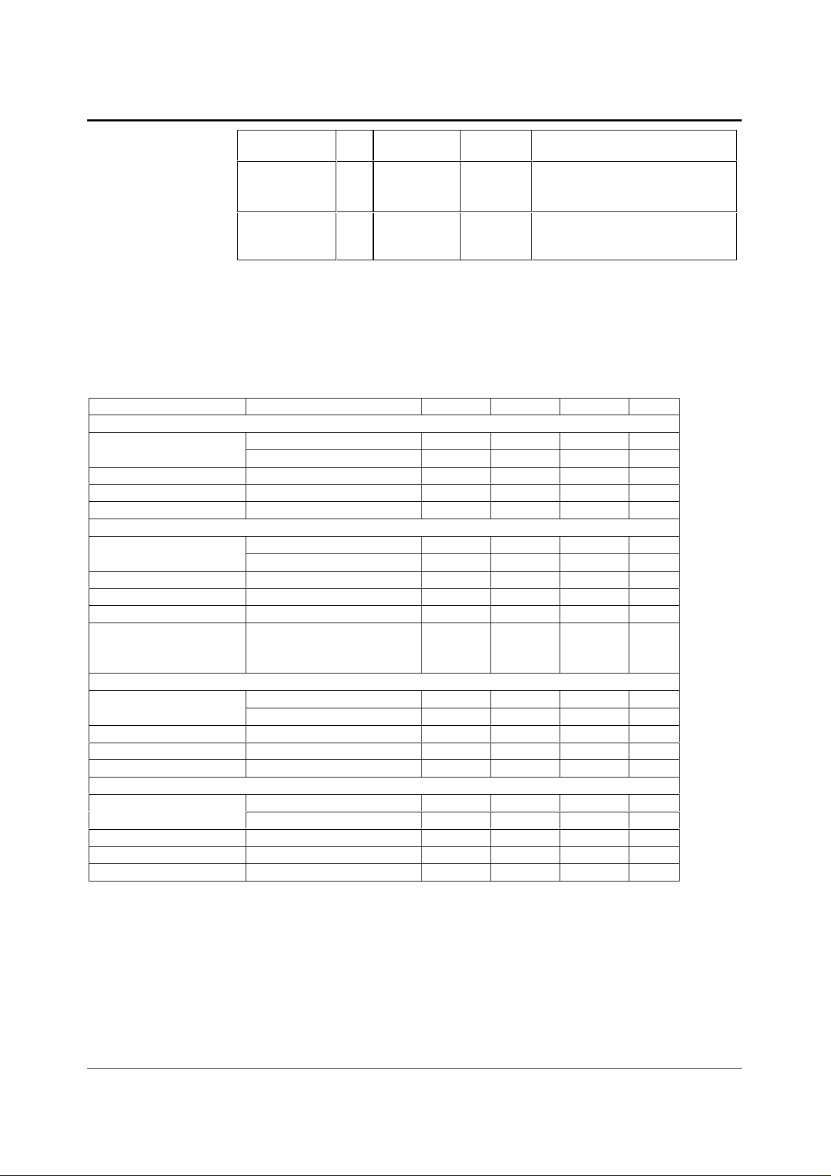
WM8731 Advanced Information
REGISTER
ADDRESS
0001001
Active Control
0001111
Reset Register
Table 29 Register Map Description
BIT LABEL DEFAULT DESCRIPTION
0 ACTIVE 0 Activate Interface
8:0 RESET not reset Reset Register
DIGITAL FILTER CHARACTERISTICS
The ADC and DAC employ different di gi tal filters. There are 4 types of digital filter, call ed Type 0, 1, 2
and 3. The performance of Types 0 and 1 is list ed in the table below, the responses of al l filters is
shown in the proceeding pages.
PARAMETER TEST CONDITIONS MIN TYP MAX UNIT
ADC Filter Type 0 (USB Mode, 250fs operation)
Passband
Passband Ripple
Stopband
Stopband Attenuation
ADC Filter Type 1 (USB mode, 272fs or Normal mode operation)
Passband
Passband Ripple
Stopband
Stopband Attenuation
High Pass Filter Corner
Frequency
DAC Filter Type 0 (USB mode, 250fs operation)
Passband
Passband Ripple
Stopband
Stopband Attenuation
DAC Filter Type 1 (USB mode, 272fs or Normal mode operation)
Passband
Passband Ripple
Stopband
Stopband Attenuation
Table 30 Digital Filter Characteristics
+/- 0.05dB 0 0.416fs
-6dB 0.5fs
f > 0.584fs -60 dB
+/- 0.05dB 0 0.4535fs
-6dB 0.5fs
f > 0.5465fs -60 dB
-3dB
-0.5dB
-0.1dB
+/- 0.03dB 0 0.416fs
-6dB 0.5fs
f > 0.584fs -50 dB
+/- 0.03dB 0 0.4535fs
-6dB 0.5fs
f > 0.5465fs -50 dB
0.584fs
0.5465fs
0.584fs
0.5465fs
1 = Active
0 = Inactive
Writing 00000000 to register resets
device
+/- 0.05 dB
+/- 0.05 dB
3.7
10.4
21.6
+/-0.03 dB
+/- 0.03 dB
Hz
TERMINOLOGY
1. Stop Band Attenuation (dB) - t he degree to which the frequency spectrum i s attenuated (outside audio band)
2. Pass-band Ripple – any variation of the frequency response in the pass-band region
WOLFSON MICROELECTRONICS LTD AI Rev 2.0 February 2001
50
Page 51
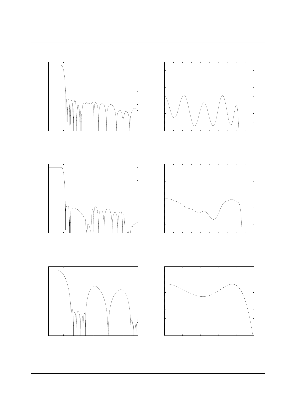
WM8731 Advanced Information
DAC FILTER RESPONSES
0
-20
0.04
0.03
0.02
-40
-60
Response (dB)
-80
-100
0 0.5 1 1.5 2 2.5 3
Frequency (Fs)
0.01
0
Response (dB)
-0.01
-0.02
-0.03
-0.04
0 0.05 0.1 0.15 0.2 0.25 0.3 0.35 0.4 0.45 0.5
Frequency (Fs)
Figure 33 DAC Digital Filter Frequency Response –Type 0 Figure 34 DAC Digital Filter Ripple –Type 0
0
-20
-40
-60
Response (dB)
-80
0.04
0.03
0.02
0.01
0
Response (dB)
-0.01
-0.02
-0.03
-100
0 0.5 1 1.5 2 2.5 3
Frequency (Fs)
-0.04
0 0.05 0.1 0.15 0.2 0.25 0.3 0.35 0.4 0.45 0.5
Frequency (Fs)
Figure 35 DAC Digital Filter Frequency Response –Type 1 Figure 36 DAC Digital Filter Ripple –Type 1
0
-20
-40
-60
Response (dB)
-80
-100
0 0.5 1 1.5 2 2.5 3
Frequency (Fs)
0.02
0.01
0
-0.01
-0.02
Response (dB)
-0.03
-0.04
-0.05
-0.06
0 0.05 0.1 0.15 0.2 0.25
Frequency (Fs)
Figure 37 DAC Digital Filter Frequency Response –Type 2 Figure 38 DAC Digital Filter Ripple –Type 2
WOLFSON MICROELECTRONICS LTD AI Rev 2.0 February 2001
51
Page 52
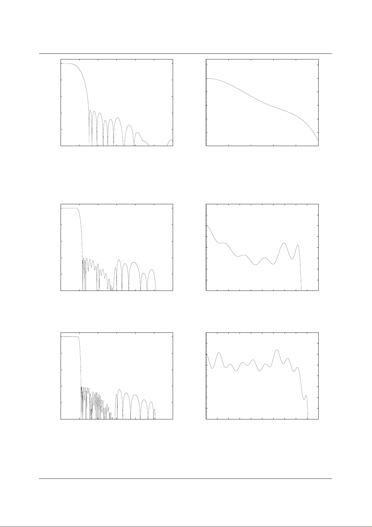
WM8731 Advanced Information
0
-20
-40
-60
Response (dB)
-80
-100
0 0.5 1 1.5 2 2.5 3
Frequency (Fs)
0.05
0
-0.05
-0.1
Response (dB)
-0.15
-0.2
-0.25
0 0.05 0.1 0.15 0.2 0.25
Frequency (Fs)
Figure 39 DAC Digital Filter Frequency Response –Type 3 Figure 40 DAC Digital Filter Ripple –Type 3
ADC FILTER RESPONSES
0
-20
-40
-60
Response (dB)
0.02
0.01
0
-0.01
-0.02
Response (dB)
-0.03
-80
-100
0 0.5 1 1.5 2 2.5 3
Frequency (Fs)
-0.04
-0.05
-0.06
0 0.05 0.1 0.15 0.2 0.25 0.3 0.35 0.4 0.45 0.5
Frequency (Fs)
Figure 41 ADC Digital Filter Frequency Response –Type 0 Figure 42 ADC Digital Filter Ripple –Type 0
0
-20
-40
-60
Response (dB)
-80
-100
0 0.5 1 1.5 2 2.5 3
Frequency (Fs)
0.02
0.01
0
-0.01
-0.02
Response (dB)
-0.03
-0.04
-0.05
-0.06
0 0.05 0.1 0.15 0.2 0.25 0.3 0.35 0.4 0.45 0.5
Frequency (Fs)
Figure 43 ADC Digital Filter Frequency Response –Type 1 Figure 44 ADC Digital Filter Ripple –Type 1
WOLFSON MICROELECTRONICS LTD AI Rev 2.0 February 2001
52
Page 53
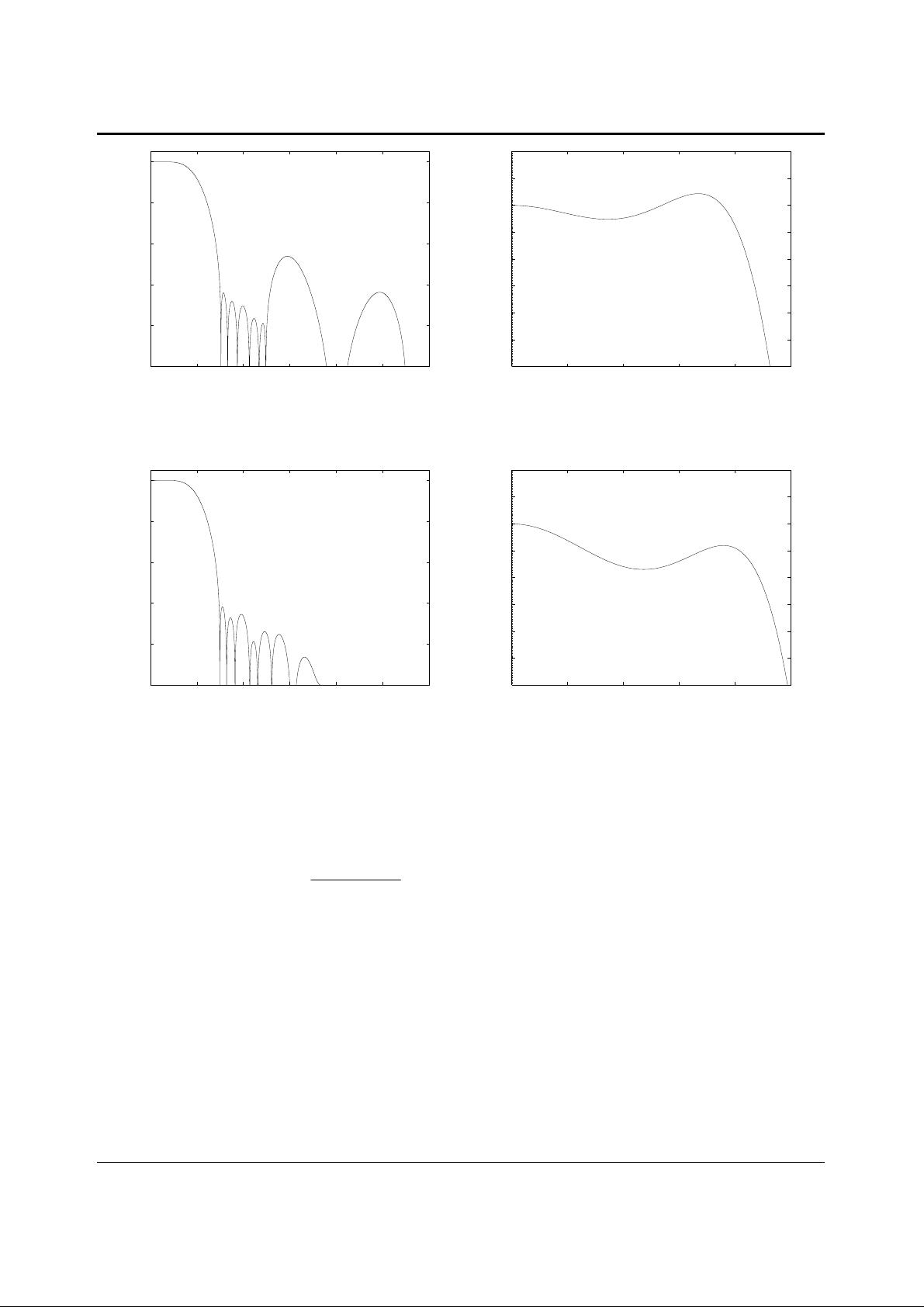
WM8731 Advanced Information
0
-20
-40
-60
Response (dB)
-80
-100
0 0.5 1 1.5 2 2.5 3
Frequency (Fs)
0.02
0.01
0
-0.01
-0.02
Response (dB)
-0.03
-0.04
-0.05
-0.06
0 0.05 0.1 0.15 0.2 0.25
Frequency (Fs)
Figure 45 ADC Digital Filter Frequency Response –Type 2 Figure 46 ADC Digital Filter Ripple –Type 2
0
-20
-40
-60
Response (dB)
0.02
0.01
0
-0.01
-0.02
Response (dB)
-0.03
-80
-100
0 0.5 1 1.5 2 2.5 3
Frequency (Fs)
-0.04
-0.05
-0.06
0 0.05 0.1 0.15 0.2 0.25
Frequency (Fs)
Figure 47 ADC Digital Filter Frequency Response –Type 3 Figure 48 ADC Digital Filter Ripple –Type 3
ADC HIGH PASS FILTER
The WM8731 has a selectable digital high pass filt er to remove DC offsets. The filter res ponse is
characterised by the foll owing polynomial.
H(z) = 1 – z
1 – 0.9995 z
-1
-1
WOLFSON MICROELECTRONICS LTD AI Rev 2.0 February 2001
53
Page 54
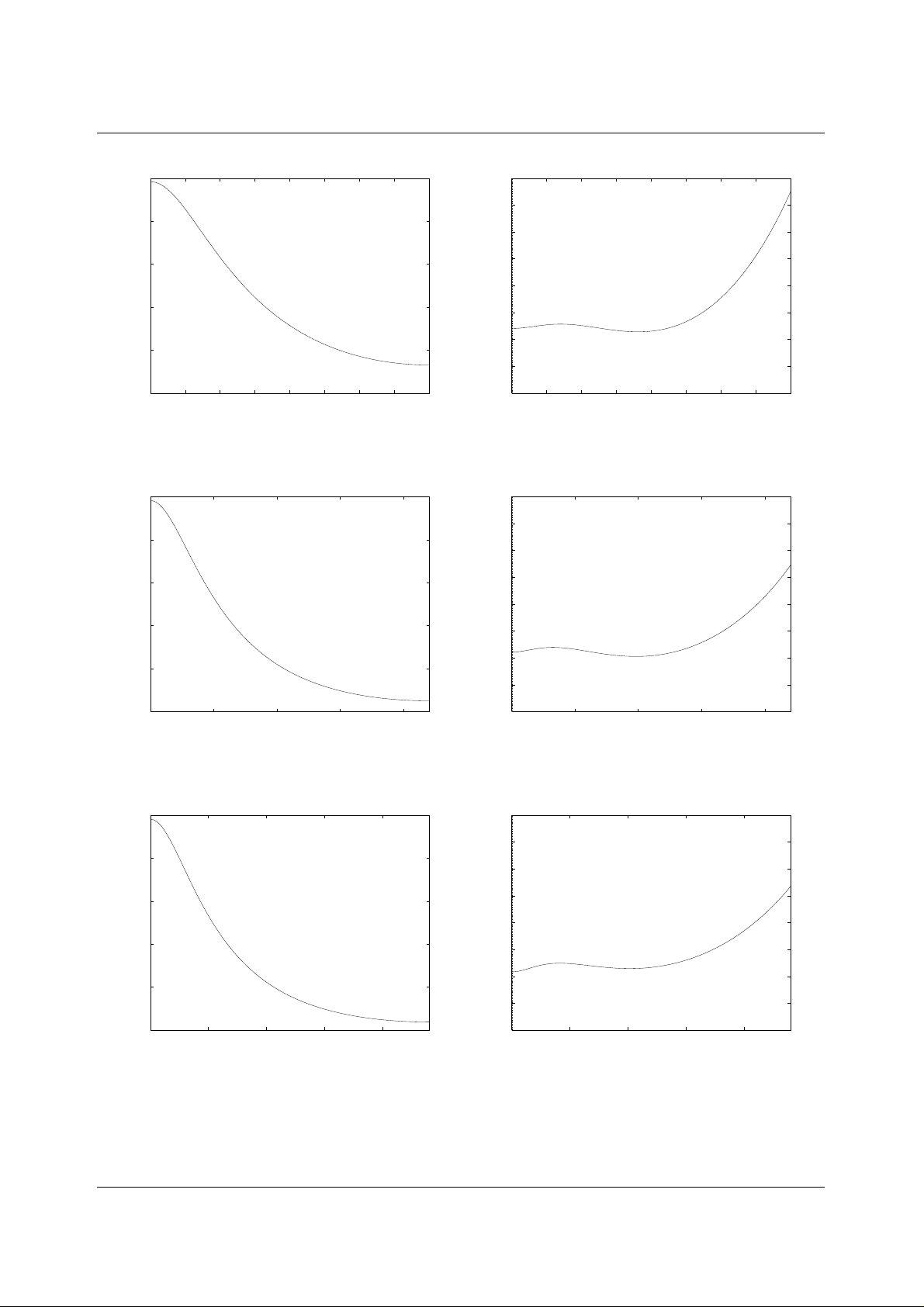
WM8731 Advanced Information DIGITAL DE-EMPHASIS CHARACTERISTICS
0
-2
0.4
0.3
0.2
-4
-6
Response (dB)
-8
-10
0 2000 4000 6000 8000 10000 12000 14000 16000
Frequency (Fs)
0.1
0
Response (dB)
-0.1
-0.2
-0.3
-0.4
0 2000 4000 6000 8000 10000 12000 14000 16000
Frequency (Fs)
Figure 49 De-Emphasis Frequency Response (32kHz) Figure 50 De-Emphasis Error (32kHz)
0
-2
-4
-6
Response (dB)
-8
0.4
0.3
0.2
0.1
0
Response (dB)
-0.1
-0.2
-0.3
-10
0 5000 10000 15000 20000
Frequency (Fs)
-0.4
0 5000 10000 15000 20000
Frequency (Fs)
Figure 51 De-Emphasis Frequency Response (44.1kHz) Figure 52 De-Emphasis Error (44.1kHz)
0
-2
-4
-6
Response (dB)
-8
-10
0 5000 10000 15000 20000
Frequency (Fs)
0.4
0.3
0.2
0.1
0
Response (dB)
-0.1
-0.2
-0.3
-0.4
0 5000 10000 15000 20000
Frequency (Fs)
Figure 53 De-Emphasis Frequency Response (48kHz) Figure 54 De-Emphasis Error (48kHz)
WOLFSON MICROELECTRONICS LTD AI Rev 2.0 February 2001
54
Page 55
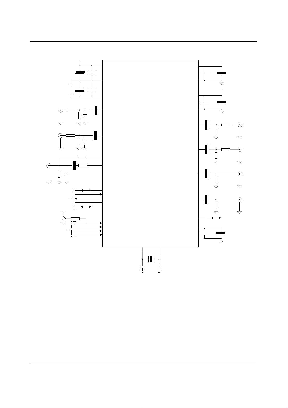
WM8731 Advanced Information RECOMMENDED EXTERNAL COMPONENTS
1.5V - 3.3V
47k
Ω
Audio Serial Data I/F
3-wire Interface
2-wire Interface
3-wire or 2-wire
MPU Interface
3.3V
5.6k
5.6k
10µF
5.6k
5.6k
220pF
10k
Ω
Ω
1µF
Ω
Ω
3.3V
+
Ω
680
Rmic
+
0.1
10µF0.1µF
+
µ
F
1
220pF
1
µ
F
220pF
Ω
1
µ
F
28
27
+
20
+
19
17
18
5
4
6
7
3
21
22
23
24
DBVDD
DGND
DCVDD
LLINEIN
RLINEIN
MICBIAS
MICIN
DACLRC
DACDAT
ADCDAT
ADCLRC
BCLK
MODE
CSB
SDIN
SCLK
WM8731
Codec
AVDD
AGND
HPVDD
HPGND
LOUT
ROUT
LHPOUT
RHPOUT
CLKOUT
VMID
14
15
8
11
+
12
+
13
+
9
220µF
+
10
220µF
2
16
µ
1
1
µ
100
0.1µF
0.1
0.1
F
F
3.3V
+
µ
F
10µF
3.3V
+
µ
F
10
µ
F
100
Ω
47k
Ω
100
Ω
47k
Ω
47k
Ω
47k
Ω
Ω
+
µ
F
10
XTOXTI/MCLK
2625
15pF15pF
Note:
1. Rmic - The value of this resistor is dependent on the gain setting. Refer to Page 20 for Rmic calculation.
2. Where possible, it is recommended that NPO or COG type capacitors should be used for best performance.
Figure 55 External Components Diagram
WOLFSON MICROELECTRONICS LTD AI Rev 2.0 February 2001
55
Page 56
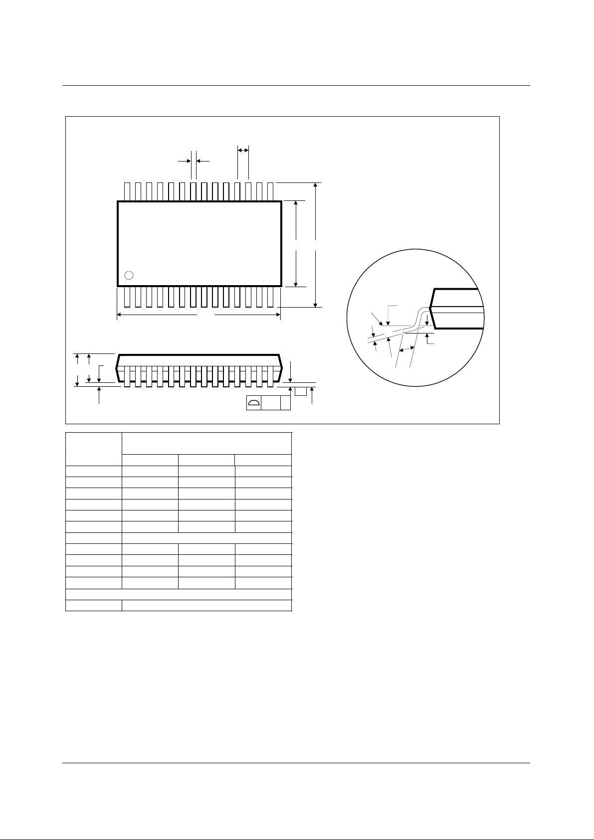
WM8731 Advanced Information PACKAGE DIMENSIONS
DM007.CDS: 28 PIN SSOP (10.2 x 5.3 x 1.75 mm)
A
A2
Symbols
A
A
1
A
2
b
c
D
e
E
E
1
L
θ
A1
b
28
1
D
Dimensions
(mm)
MIN NOM MAX
----- ----- 2.0
0.05 ----- -----
1.62 1.75 1.85
0.22 ----- 0.38
0.09 ----- 0.25
9.90 10.20 10.50
0.65 BSC
7.40 7.80 8.20
5.00 5.30 5.60
0.55 0.75 0.95
o
0
o
4
e
15
E1 E
8
14
0.10
o
-C-
C
SEATING PLANE
GAUGE
PLANE
Θ
0.25
c
L
REF:
NOTES:
A. ALL LINEAR DIMENSIONS ARE IN MILLIMETERS.
B. THIS DRAWING IS SUBJECT TO CHANGE WITHOUT NOTICE.
C. BODY DIMENSIONS DO NOT INCLUDE MOLD FLASH OR PROTRUSION, NOT TO EXCEED 0.20MM.
D. MEETS JEDEC.95 MO-150, VARIATION = AH. REFER TO THIS SPECIFICATION FOR FURTHER DETAILS.
JEDEC.95, MO-150
WOLFSON MICROELECTRONICS LTD AI Rev 2.0 February 2001
56
Page 57

 Loading...