

White Electronic Designs WEDPNF8M721V-1010BI, WEDPNF8M721V-1010BC, WEDPNF8M721V-1215BM, WEDPNF8M721V-1215BI, WEDPNF8M721V-1215BC Datasheet
...
White Electronic Designs
WEDPNF8M721V-XBX
8Mx72 Synchronous DRAM + 8Mb Flash Mixed Module
Multi-Chip Package
ADVANCED*
FEATURES
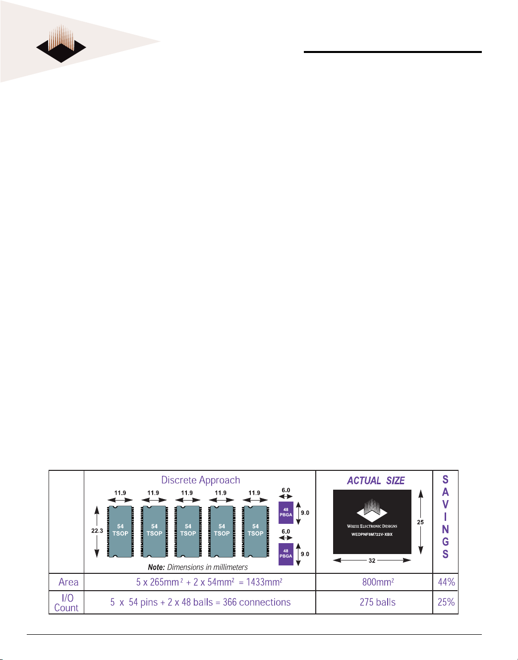
n Package:
• 275 Plastic Ball Grid Array (PBGA), 32mm x 25mm
n Commercial, Industrial and Military Temperature Ranges
n Weight:
• WEDPNF8M721V-XBX - 2.5 grams typical
SDRAM PERFORMANCE FEATURES
n Organized as 8M x 72
n High Frequency = 100, 125MHz
n Single 3.3V ±0.3V power supply
n Fully Synchronous; all signals registered on positive
edge of system clock cycle
n Internal pipelined operation; column address can be
changed every clock cycle
n Internal banks for hiding row access/precharge
n Programmable Burst length 1,2,4,8 or full page
n 4096 refresh cycles
FLASH PERFORMANCE FEATURES
n User Configurable as 1Mx8 or 512Kx16
n Access Times of 100, 120, 150ns
n 3.3 Volt for Read and Write Operations
n 1,000,000 Erase/Program Cycles
n Sector Architecture
• One 16KByte, two 8KBytes, one 32KByte, and fif
teen 64KBytes in byte mode
• One 8K word, two 4K words, one 16K word, and
fifteen 32K word sectors in word mode.
• Any combination of sectors can be concurrently
erased. Also supports full chip erase
n Boot Code Sector Architecture (Bottom)
n Embedded Erase and Program Algorithms
n Erase Suspend/Resume
• Supports reading data from or programing data to a
sector not being erased
BENEFITS
n 42% SPACE SAVINGS
n Reduced part count
n Reduced I/O count
• 14% I/O Reduction
n Suitable for hi-reliability applications
n SDRAM Upgradeable to 16M x 72 density (contact
factory for information)
n Flash upgradeable to 2M x 8 (or 1M x 16 or 512K x 32)
density
* This data sheet describes a product that may or may not be under
development and is subject to change or cancellation without notice.
September 2002 Rev. 3
11
1 White Electronic Designs Corporation • (602) 437-1520 • www.whiteedc.com
11
White Electronic Designs
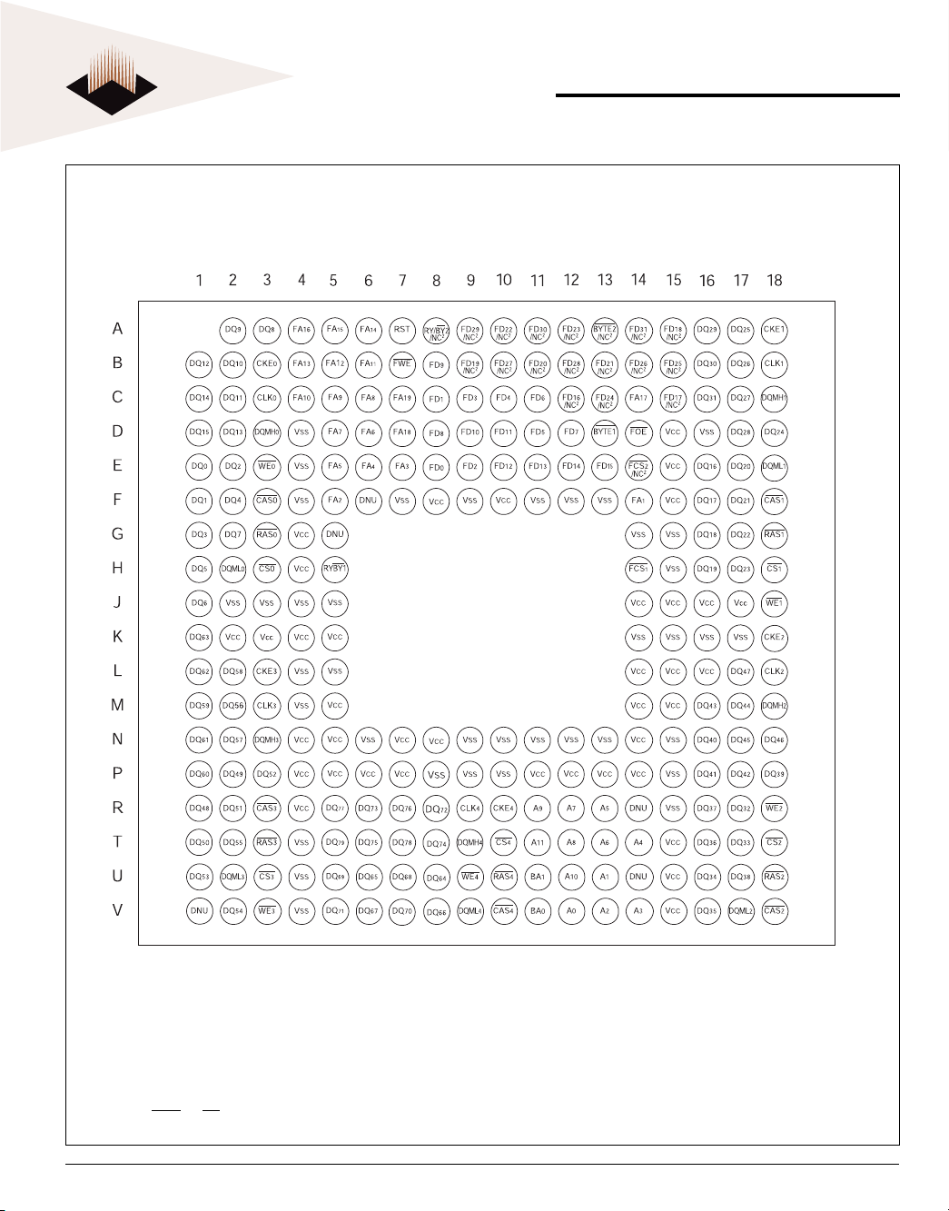
FIG. 1 PIN CONFIGURATION
WEDPNF8M721V-XBX
TOP VIEW
NOTES:
1. DNU = Do Not Use
2. FD16-31, BYTE2, RY/BY2 are NC in this part, and used for flash upgraded to WEDPN8M722V-XBX (2x8M Flash).
22
2
White Electronic Designs Corporation • Phoenix AZ • (602) 437-1520
22
White Electronic Designs
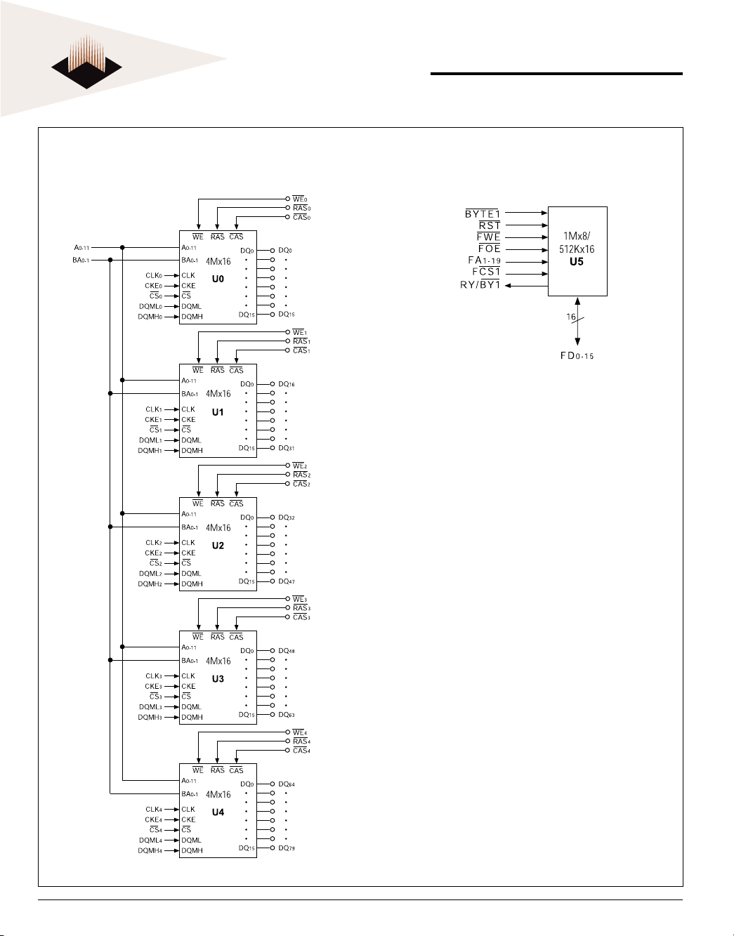
FIG. 2 FUNCTIONAL BLOCK DIAGRAMS
WEDPNF8M721V-XBX
SDRAM
FLASH
33
3 White Electronic Designs Corporation • (602) 437-1520 • www.whiteedc.com
33

White Electronic Designs
WEDPNF8M721V-XBX
PACKAGE PINOUT LISTING
Signal NameSignal Name
Signal Name
Signal NameSignal Name
CC D15, E15, F8, F10, F15, G4, H4, J14, J15, J16, J17, K2, K3, K4, K5, L14, L15, L16, M5, M14, M15, N4, N5, N7, N8, N14, P4, P5, P6,
V
GND D4, D16, E4, F4, F7, F9, F11, F12, F13, G14, G15, H15, J2, J3, J4, J5, K14, K15, K16, K17, L4, L5, M4, N6, N9, N10, N11, N12, N13,
FD0 - 15 E8, C8, E9, C9, C10, D11, C11, D12, D8, B8, D9, D10, E10, E11, E12, E13
RYBY1 H5
RST A7
BYTE1 D13
FD16* - 31* C12, C15, A15, B9, B11, B13, A10, A12, C13, B15, B14, B10, B12, A9, A11, A14
RYBY2* A8
BYTE2* A13
FA1-19 F14, F5, E7, E6, E5, D6, D5, C6, C5, C4, B6, B5, B4, A6, A5, A4, C14, D7, C7
FCS1 H14
FCS2* E14
FWE B7
FOE D14
A0 - A11 V12, U13, V13, V14, T14, R13, T13, R12, T12, R11, U12, T11
BA0 - 1 U11, V11
CS0 H3
WE0 E3
CLK0 C3
CKE0 B3
RAS0 G3
CAS0 F3
DQML0 H2
DQMH0 D3
CS1 H18
WE1 J18
CLK1 B18
CKE1 A18
RAS1 G18
CAS1 F18
DQML1 E18
DQMH1 C18
CS2 T18
WE2 R18
CLK2 L18
CKE2 K18
RAS2 U18
CAS2 V18
DQML2 V17
DQMH2 M18
CS3 U3
WE3 V3
CLK3 M3
CKE3 L3
RAS3 T3
White Electronic Designs Corporation • Phoenix AZ • (602) 437-1520
P7, P11, P12, P13, P14, R4, T15, U15, V15
N15, P8, P9, P10, P15, R15, T4, U4, V4
Pin NumberPin Number
Pin Number
Pin NumberPin Number
*FD16-31, RY/BY2, BYTE2 are NC in this par t, and used for flash upgrade to WEDPNF8M722V-XBX
44
4
44

White Electronic Designs
WEDPNF8M721V-XBX
PACKAGE PINOUT LISTING (CONTINUED)
Signal NameSignal Name
Signal Name
Signal NameSignal Name
CAS3 R3
DQML3 U2
DQMH3 N3
CS4 T10
WE4 U9
CLK4 R9
CKE4 R10
RAS4 U10
CAS4 V10
DQML4 V9
DQMH4 T9
DQ0 - 15 E1, F1, E2, G1, F2, H1, J1, G2, A3, A2, B2, C2, B1, D2, C1, D1,
DQ16 - 31 E16, F16, G16, H16, E17, F17, G17, H17, D18, A17, B17, C17, D17, A16, B16, C16
DQ32 - 47 R17, T17, U16, V16, T16, R16, U17, P18, N16, P16, P17, M16, M17, N17, N18, L17
DQ48 - 63 R1, P2, T1, R2, P3, U1, V2, T2, M2, N2, L2, M1, P1, N1, L1, K1
DQ64 - 79 U8, U6, V5, V6, U7, U5, V7, V8, R8, R6, T8, T6, R7, R5, T7, T5
DNU F6, G5, R14, U14, V1
Pin NumberPin Number
Pin Number
Pin NumberPin Number
55
5 White Electronic Designs Corporation • (602) 437-1520 • www.whiteedc.com
55
White Electronic Designs
WEDPNF8M721V-XBX
ABSOLUTE MAXIMUM RATINGS
PP
arameterarameter
P
arameter
PP
arameterarameter
Supply Voltage Range (VCC) -0.5 to +4.0 V
Signal Voltage Range -0.5 to Vcc +0.5 V
Operating Temperature TA (Mil) -55 to +125 °C
Operating Temperature TA (Ind) -40 to +85 °C
Storage Temperature, Plastic -65 to +150 °C
Flash Endurance (write/erase cycles) 1,000,000 min. cycles
NOTE:
Stress greater than those listed under "Absolute Maximum Ratings" may cause
permanent damage to the device. This is a stress rating only and functional
operation of the device at these or any other conditions greater than those
indicated in the operational sections of this specification is not implied.
Exposure to absolute maximum rating conditions for extended periods may
affect reliability.
UnitUnit
Unit
UnitUnit
PP
arameterarameter
P
arameter
PP
arameterarameter
Input Capacitance: CLK CI1 10 pF
Addresses, BA0-1 Input Capacitance CA 35 pF
Input Capacitance: All other input-only pins CI2 10 pF
Input/Output Capacitance: I/Os C
ParameterParameter
Parameter
ParameterParameter
Minimum Pattern Data 150°C 10 Years
Retention Time 125°C 20 Years
SDRAM CAPACITANCE (NOTE 2)
SymbolSymbol
Symbol
SymbolSymbol
IO 12 pF
FLASH DATA RETENTION
Test ConditionsTest Conditions
Test Conditions
Test ConditionsTest Conditions
MinMin
Min
MinMin
MaxMax
Max
MaxMax
DC ELECTRICAL CHARACTERISTICS AND OPERATING CONDITIONS (NOTES 1, 3)
(VCC = +3.3V ±0.3V; TA = -55°C TO +125°C)
Parameter/ConditionParameter/Condition
Parameter/Condition
Parameter/ConditionParameter/Condition
Supply Voltage VCC 3 3.6 V
Input High Voltage: Logic 1; All inputs (4) VIH 0.7 x Vcc VCC + 0.3 V
Input Low Voltage: Logic 0; All inputs (4) VIL -0.3 0.8 V
SDRAMSDRAM
SDRAM
SDRAMSDRAM
Input Leakage Current: Any input 0V ≤ V
(All other pins not under test = 0V)
SDRAM Input Leakage Address Current
(All other pins not under test = 0V) II -25 25 µA
SDRAM Output Leakage Current: I/Os are disabled; 0V ≤ V OUT ≤ VCC IOZ -5 5 µA
SDRAM Output High Voltage (IOUT = -4mA) VOH 2.4 – V
SDRAM Output Low Voltage (IOUT = 4mA) VOL – 0.4 V
FlashFlash
Flash
FlashFlash
Flash Input Leakage Current (VCC = 3.6, VIN = GND or VCC) ILI 10 µA
Flash Output Leakage Current (VCC = 3.6, VIN = GND or VCC) ILOx8 10 µA
Flash Output High Voltage (IOH = -2.0 mA, VCC = 3.0) VOH1 0.85 X VCC V
Flash Output Low Voltage (IOL = 5.8 mA, VCC = 3.0) VOL 0.45 V
Flash Low V
NOTES:
1. All voltages referenced to VSS.
2. This parameter is not tested but guaranteed by design. f = 1 MHz, TA = 25°C.
3. An initial pause of 100ms is required after power-up, followed by two AUTO REFRESH commands, before proper device operation is ensured. (VCC must be
powered up simultaneously.) The two AUTO REFRESH command wake-ups should be repeated any time the tREF refresh requirement is exceeded.
4. VIH overshoot: VIH (MAX) = VCC + 2V for a pulse width ≤ 3ns, and the pulse width cannot be greater than one third of the cycle rate. VIL undershoot: VIL
(MIN) = -2V for a pulse width ≤ 3ns.
5. Guaranteed by design, but not tested.
CC Lock-Out Voltage (5) VLKO 2.3 2.5 V
IN
≤
V CC II -5 5 µA
SymbolSymbol
Symbol
SymbolSymbol
MinMin
Min
MinMin
MaxMax
Max
MaxMax
UnitsUnits
Units
UnitsUnits
UnitUnit
Unit
UnitUnit
UnitUnit
Unit
UnitUnit
White Electronic Designs Corporation • Phoenix AZ • (602) 437-1520
66
6
66
White Electronic Designs
WEDPNF8M721V-XBX
ICC SPECIFICATIONS AND C ONDITIONS (NOTES 1,2,3,4)
(VCC = +3.3V ±0.3V; TA = -55°C TO +125°C)
Parameter/ConditionParameter/Condition
Parameter/Condition
Parameter/ConditionParameter/Condition
SDRAM Operating Current: Active Mode;
Burst = 2; Read or Write; tRC = tRC (min); CAS latency = 3 (5, 6, 7); FCS = High
SDRAM Standby Current: Active Mode; CKE = HIGH; CS = HIGH; FCS = High;
All banks active after tRCD met; No accesses in progress (5, 7, 8)
SDRAM Operating Current: Burst Mode; Continuous burst; FCS = High
Read or Write; All banks active; CAS latency = 3 (5, 6, 7)
SDRAM Self Refresh Current; FCS = High (14) ICC7 10 mA
Flash VCC Active Current for Read : FCS = VIL, FOE = VIH, f = 5MHz (9), CS = High, CKE = Low IFCC1 32 mA
Flash VCC Active Current for Program or Erase: FCS = VIL, FOE = VIH, CS = High, CKE = Low IFCC2 50 mA
Standby Current: VCC = 3.6 Max, FCS = VIH, CS = High, CKE = Low ICC3 20 mA
NOTES:
1. All voltages referenced to VSS.
2. An initial pause of 100ms is required after power-up, followed by two
AUTO REFRESH commands, before proper device operation is ensured. (VCC
must be powered up simultaneously.) The two AUTO REFRESH command
wake-ups should be repeated any time the tREF refresh requirement is
exceeded.
3. AC timing and ICC tests have VIL = 0V and VIH = 3V, with timing referenced
to 1.5V crossover point.
4. ICC specifications are tested after the device is properly initialized.
5. ICC is dependent on output loading and cycle rates. Specified values are
obtained with minimum cycle time and the outputs open.
6. The ICC current will decrease as the CAS latency is reduced. This is due to
the fact that the maximum cycle rate is slower as the CAS latency is reduced.
7. Address transitions average one transition every two clocks.
8. Other input signals are allowed to transition no more than once every two
clocks and are otherwise at valid VIH or VIL levels.
9. The ICC current listed includes both the DC operating current and the
frequency dependent component (at 5 MHz). The frequency component
typically is less than 8 mA/MHz, with OE at VIH.
10. ICC active while Embedded Algorithm (program or erase) is in progress.
11. Maximum ICC specifications are tested with VCC = VCC Max.
12. Automatic sleep mode enables the low power mode when addressed
remain stable for tacc + 30 ns.
13. SDRAM inactive and in Power Down mode, all banks idle.
14. Self refresh available in commercial and industrial temperatures only.
SymbolSymbol
Symbol
SymbolSymbol
CC1 750 mA
I
CC3 250 mA
I
CC4 750 mA
I
MaxMax
Max
MaxMax
UnitsUnits
Units
UnitsUnits
SDRAM DESCRIPTION
The 64MByte (512Mb) SDRAM is a high-speed CMOS, dynamic random-access ,memory using 5 chips containing
134, 217, 728 bits. Each chip is internally configured as a
quad-bank DRAM with a synchronous interface. Each of the
chip’s 33,554,432-bit banks is organized as 4,096 rows by
512 columns by 16 bits.
Read and write accesses to the SDRAM are burst oriented;
accesses start at a selected location and continue for a programmed number of locations in a programmed sequence.
Accesses begin with the registration of an ACTIVE command, which is then followed by a READ or WRITE command. The address bits registered coincident with the ACTIVE command are used to select the bank and row to be
accessed (BA0, BA1 select the bank; A0-11 select the row).
The address bits registered coincident with the READ or
WRITE command are used to select the starting column location for the burst access.
The SDRAM provides for programmable READ or WRITE burst
lengths of 1, 2, 4 or 8 locations, or the full page, with a
burst terminate option. An AUTO PRECHARGE function may
be enabled to provide a self-timed row precharge that is
initiated at the end of the burst sequence.
The 64MB SDRAM uses an internal pipelined architecture to
achieve high-speed operation. This architecture is compat-
n
ible with the 2
rule of prefetch architectures, but it also
allows the column address to be changed on every clock
cycle to achieve a high-speed, fully random access.
Precharging one bank while accessing one of the other three
banks will hide the precharge cycles and provide seamless, high-speed, random-access operation.
The 64MB SDRAM is designed to operate in 3.3V, lowpower memory systems. An auto refresh mode is provided,
along with a power-saving, power-down mode.
All inputs and outputs are LVTTL compatible. SDRAMs offer
substantial advances in DRAM operating performance, including the ability to synchronously burst data at a high data
rate with automatic column-address generation, the ability
to interleave between internal banks in order to hide
precharge time and the capability to randomly change column addresses on each clock cycle during a burst access.
SDRAM FUNCTIONAL DESCRIPTION
Read and write accesses to the SDRAM are burst oriented;
accesses start at a selected location and continue for a programmed number of locations in a programmed sequence.
77
7 White Electronic Designs Corporation • (602) 437-1520 • www.whiteedc.com
77

White Electronic Designs
WEDPNF8M721V-XBX
Accesses begin with the registration of an ACTIVE command which is then followed by a READ or WRITE command. The address bits registered coincident with the ACTIVE command are used to select the bank and row to be
accessed (BA0 and BA1 select the bank, A0-11 select the
row). The address bits (A0-8) registered coincident with
the READ or WRITE command are used to select the starting column location for the burst access.
Prior to normal operation, the SDRAM must be initialized.
The following sections provide detailed information covering device initialization, register definition, command descriptions and device operation.
INITIALIZATION
SDRAMs must be powered up and initialized in a predefined
manner. Operational procedures other than those specified may result in undefined operation. Once power is applied to VDD and VDDQ (simultaneously) and the clock is
stable (stable clock is defined as a signal cycling within timing constraints specified for the clock pin), the SDRAM requires a 100µs delay prior to issuing any command other
than a COMMAND INHIBIT or a NOP. Starting at some point
during this 100µs period and continuing at least through
the end of this period, COMMAND INHIBIT or NOP commands should be applied.
Once the 100µs delay has been satisfied with at least one
COMMAND INHIBIT or NOP command having been applied,
a PRECHARGE command should be applied. All banks must
be precharged, thereby placing the device in the all banks
idle state.
Once in the idle state, two AUTO REFRESH cycles must be
performed. After the AUTO REFRESH cycles are complete, the
SDRAM is ready for Mode Register programming. Because the
Mode Register will power up in an unknown state, it should
be loaded prior to applying any operational command.
REGISTER DEFINITION
MODE REGISTER
The Mode Register is used to define the specific mode of
operation of the SDRAM. This definition includes the selection of a burst length, a burst type, a CAS latency, an operating mode and a write burst mode, as shown in Figure 3.
The Mode Register is programmed via the LOAD MODE REGISTER command and will retain the stored information until
it is programmed again or the device loses power.
Mode register bits M0-M2 specify the burst length, M3
specifies the type of burst (sequential or interleaved), M4-
M6 specify the CAS latency, M7 and M8 specify the operating mode, M9 specifies the WRITE burst mode, and M10
and M11 are reserved for future use.
The Mode Register must be loaded when all banks are idle,
and the controller must wait the specified time before initiating the subsequent operation. Violating either of these
requirements will result in unspecified operation.
BURST LENGTH
Read and write accesses to the SDRAM are burst oriented,
with the burst length being programmable, as shown in Figure 3. The burst length determines the maximum number of
column locations that can be accessed for a given READ or
WRITE command. Burst lengths of 1, 2, 4 or 8 locations are
available for both the sequential and the interleaved burst
types, and a full-page burst is available for the sequential
type. The full-page burst is used in conjunction with the
BURST TERMINATE command to generate arbitrary burst
lengths.
Reserved states should not be used, as unknown operation or incompatibility with future versions may result.
When a READ or WRITE command is issued, a block of columns equal to the burst length is effectively selected. All
accesses for that burst take place within this block, meaning that the burst will wrap within the block if a boundary is
reached. The block is uniquely selected by A1-8 when the
burst length is set to two; by A2-8 when the burst length is
set to four; and by A3-8 when the burst length is set to
eight. The remaining (least significant) address bit(s) is (are)
used to select the starting location within the block. Fullpage bursts wrap within the page if the boundary is reached.
BURST TYPE
Accesses within a given burst may be programmed to be
either sequential or interleaved; this is referred to as the
burst type and is selected via bit M3.
The ordering of accesses within a burst is determined by
the burst length, the burst type and the starting column
address, as shown in Table 1.
CAS LATENCY
The CAS latency is the delay, in clock cycles, between the
registration of a READ command and the availability of the
first piece of output data. The latency can be set to two or
three clocks.
n
If a READ command is registered at clock edge
latency is
m
clocks, the data will be available by clock edge
, and the
White Electronic Designs Corporation • Phoenix AZ • (602) 437-1520
88
8
88
White Electronic Designs
FIG. 3 MODE REGISTER DEFINITION
WEDPNF8M721V-XBX
TABLE 1 - BURST DEFINITION
Burst Starting Column Order o f Accesses Within a Burst
Length Address
2 0 0-1 0-1
A1 A0
0 0 0-1-2-3 0-1-2-3
4 0 1 1-2-3-0 1-0-3-2
1 0 2-3-0-1 2-3-0-1
1 1 3-0-1-2 3-2-1-0
A2 A1 A0
0 0 0 0-1-2-3-4-5-6-7 0-1-2-3-4-5-6-7
0 0 1 1-2-3-4-5-6-7-0 1-0-3-2-5-4-7-6
0 1 0 2-3-4-5-6-7-0-1 2-3-0-1-6-7-4-5
8 0 1 1 3-4-5-6-7-0-1-2 3-2-1-0-7-6-5-4
1 0 0 4-5-6-7-0-1-2-3 4-5-6-7-0-1-2-3
1 0 1 5-6-7-0-1-2-3-4 5-4-7-6-1-0-3-2
1 1 0 6-7-0-1-2-3-4-5 6-7-4-5-2-3-0-1
1 1 1 7-0-1-2-3-4-5-6 7-6-5-4-3-2-1-0
Full n = A0-9/8/7 Cn, Cn + 1, Cn + 2
Page Cn + 3, Cn + 4... Not Supported
(y) (location 0-y) …Cn - 1,
NOTES:
1. For full-page accesses: y = 512.
2. For a burst length of two, A1-8 select the block-of-two burst; A0 selects the
starting column within the block.
3. For a burst length of four, A2-8 select the block-of-four burst; A0-1 select the
starting column within the block.
4. For a burst length of eight, A3-8 select the block-of-eight burst; A0-2 select
the starting column within the block.
5. For a full-page burst, the full row is selected and A0-8 select the starting
column.
6. Whenever a boundary of the block is reached within a given sequence
above, the following access wraps within the block.
7. For a burst length of one, A0-8 select the unique column to be accessed, and
Mode Register bit M3 is ignored.
Type = Sequential Type = Interleaved
A0
1 1-0 1-0
Cn…
99
9 White Electronic Designs Corporation • (602) 437-1520 • www.whiteedc.com
99
White Electronic Designs
FIG. 4 CAS LATENCY
WEDPNF8M721V-XBX
n
+m. The I/Os will start driving as a result of the clock edge
n + m
one cycle earlier (
- 1), and provided that the relevant access times are met, the data will be valid by clock
edge
n + m
. For example, assuming that the clock cycle
time is such that all relevant access times are met, if a READ
command is registered at T0 and the latency is programmed
to two clocks, the I/Os will start driving after T1 and the
data will be valid by T2. Table 2 indicates the operating frequencies at which each CAS latency setting can be used.
Reserved states should not be used as unknown operation
or incompatibility with future versions may result.
OPERATING MODE
The normal operating mode is selected by setting M7and M8
to zero; the other combinations of values for M7 and M8 are
reserved for future use and/or test modes. The programmed
burst length applies to both READ and WRITE bursts.
Test modes and reserved states should not be used because unknown operation or incompatibility with future
versions may result.
WRITE BURST MODE
When M9 = 0, the burst length programmed via M0-M2
applies to both READ and WRITE bursts; when M9 = 1, the
programmed burst length applies to READ bursts, but write
accesses are single-location (nonburst) accesses.
COMMANDS
The Truth Table provides a quick reference of available commands. This is followed by a written description of each
command. Three additional Truth Tables appear following
the Operation section; these tables provide current state/
next state information.
TABLE 2 - CAS LATENCY
ALLOWABLE OPERATINGALLOWABLE OPERATING
ALLOWABLE OPERATING
ALLOWABLE OPERATINGALLOWABLE OPERATING
FREQUENCY (MHZ)FREQUENCY (MHZ)
FREQUENCY (MHZ)
FREQUENCY (MHZ)FREQUENCY (MHZ)
CASCAS
CAS
SPEEDSPEED
SPEED
SPEEDSPEED
-100 ≤ 75 ≤ 100
-125 ≤ 100 ≤ 125
CASCAS
LATENCY = 2LATENCY = 2
LATENCY = 2
LATENCY = 2LATENCY = 2
CASCAS
CAS
CASCAS
LATENCY = 3LATENCY = 3
LATENCY = 3
LATENCY = 3LATENCY = 3
COMMAND INHIBIT
The COMMAND INHIBIT function prevents new commands
from being executed by the SDRAM, regardless of whether
the CLK signal is enabled. The SDRAM is effectively deselected. Operations already in progress are not affected.
NO OPERATION (NOP)
The NO OPERATION (NOP) command is used to perform a
NOP to an SDRAM which is selected (CS is LOW). This pre-
White Electronic Designs Corporation • Phoenix AZ • (602) 437-1520
1010
10
1010
White Electronic Designs
TABLE 3 TRUTH TABLE - COMMANDS AND DQM OPERATION (NOTE 1)
WEDPNF8M721V-XBX
NAME (FUNCTION)NAME (FUNCTION)
NAME (FUNCTION)
NAME (FUNCTION)NAME (FUNCTION)
COMMAND INHIBIT (NOP) H X X X X X X
NO OPERATION (NOP) L H H H X X X
ACTIVE (Select bank and activate row) ( 3) L L H H X Bank/Row X
READ (Select bank and column, and start READ burst) (4) L H L H L/ H
WRITE (Select bank and column, and start WRITE burst) (4) L H L L L/H
BURST TERMINATE L H H L X X Active
PRECHARGE (Deactivate row in bank or banks) ( 5) L L H L X Code X
AUTO REFRESH or SELF REFRESH (Enter self refresh mode) (6, 7) L L L H X X X
LOAD MODE REGISTER (2) L L L L X Op-Code X
Write Enable/Output Enable (8) – – – – L – Active
Write Inhibit/Output High-Z (8) – – – – H – High-Z
NOTES:
1. CKE is HIGH for all commands shown except SELF REFRESH.
2. A0-11 define the op-code written to the Mode Register.
3. A0-11 provide row address, and BA0, BA1 determine which bank is made active.
4. A0-8 provide column address; A10 HIGH enables the auto precharge feature (nonpersistent), while A10 LOW disables the auto precharge feature; BA0, BA1
determine which bank is being read from or written to.
5. A10 LOW: BA0, BA1 determine the bank being precharged. A10 HIGH: All banks precharged and BA0, BA1 are “Don’t Care.”
6. This command is AUTO REFRESH if CKE is HIGH; SELF REFRESH if CKE is LOW.
7. Internal refresh counter controls row addressing; all inputs and I/Os are “Don’t Care” except for CKE.
8. Activates or deactivates the I/Os during WRITEs (zero-clock delay) and READs (two-clock delay).
vents unwanted commands from being registered during
idle or wait states. Operations already in progress are not
affected.
CSCS
CS
CSCS
RASRAS
RAS
RASRAS
CASCAS
CAS
CASCAS
WEWE
WE
WEWE
DQMDQM
DQM
DQMDQM
ADDRADDR
ADDR
ADDRADDR
8
Bank/Col X
8
Bank/Col Valid
mines whether or not AUTO PRECHARGE is used. If AUTO
PRECHARGE is selected, the row being accessed will be
precharged at the end of the READ burst; if AUTO
PRECHARGE is not selected, the row will remain open for
LOAD MODE REGISTER
The Mode Register is loaded via inputs A0-11. See Mode
Register heading in the Register Definition section. The LOAD
MODE REGISTER command can only be issued when all
banks are idle, and a subsequent executable command
cannot be issued until tMRD is met.
ACTIVE
The ACTIVE command is used to open (or activate) a row in
a particular bank for a subsequent access. The value on the
BA0, BA1 inputs selects the bank, and the address provided on inputs A0-11 selects the row. This row remains
active (or open) for accesses until a PRECHARGE command
is issued to that bank. A PRECHARGE command must be
issued before opening a different row in the same bank.
READ
The READ command is used to initiate a burst read access
to an active row. The value on the BA0, BA1 inputs selects
the bank, and the address provided on inputs A0-8 selects
the starting column location. The value on input A10 deter-
subsequent accesses. Read data appears on the I/Os subject to the logic level on the DQM inputs two clocks earlier.
If a given DQM signal was registered HIGH, the corresponding I/Os will be High-Z two clocks later; if the DQM signal
was registered LOW, the I/Os will provide valid data.
WRITE
The WRITE command is used to initiate a burst write access
to an active row. The value on the BA0, BA1 inputs selects
the bank, and the address provided on inputs A0-8 selects the starting column location. The value on input A10
determines whether or not AUTO PRECHARGE is used. If
AUTO PRECHARGE is selected, the row being accessed will
be precharged at the end of the WRITE burst; if AUTO
PRECHARGE is not selected, the row will remain open for
subsequent accesses. Input data appearing on the I/Os is
written to the memory array subject to the DQM input logic
level appearing coincident with the data. If a given DQM
signal is registered LOW, the corresponding data will be
written to memory; if the DQM signal is registered HIGH,
the corresponding data inputs will be ignored, and a WRITE
will not be executed to that byte/column location.
I/OsI/Os
I/Os
I/OsI/Os
1111
11 White Electronic Designs Corporation • (602) 437-1520 • www.whiteedc.com
1111

White Electronic Designs
WEDPNF8M721V-XBX
PRECHARGE
The PRECHARGE command is used to deactivate the open
row in a particular bank or the open row in all banks. The
bank(s) will be available for a subsequent row access a
specified time (tRP) after the PRECHARGE command is issued. Input A10 determines whether one or all banks are
to be precharged, and in the case where only one bank is
to be precharged, inputs BA0, BA1 select the bank. Otherwise BA0, BA1 are treated as “Don’t Care.” Once a bank
has been precharged, it is in the idle state and must be
activated prior to any READ or WRITE commands being issued to that bank.
AUTO PRECHARGE
AUTO PRECHARGE is a feature which performs the same
individual-bank PRECHARGE function described above,
without requiring an explicit command. This is accomplished
by using A10 to enable AUTO PRECHARGE in conjunction
with a specific READ or WRITE command. A precharge of
the bank/row that is addressed with the READ or WRITE command is automatically performed upon completion of the
READ or WRITE burst, except in the full-page burst mode,
where AUTO PRECHARGE does not apply. AUTO
PRECHARGE is nonpersistent in that it is either enabled or
disabled for each individual READ or WRITE command.
AUTO PRECHARGE ensures that the precharge is initiated at
the earliest valid stage within a burst. The user must not issue
another command to the same bank until the precharge time
(tRP) is completed. This is determined as if an explicit
PRECHARGE command was issued at the earliest possible time.
BURST TERMINATE
The BURST TERMINATE command is used to truncate either
fixed-length or full-page bursts. The most recently registered
READ or WRITE command prior to the BURST TERMINATE
command will be truncated.
AUTO REFRESH
AUTO REFRESH is used during normal operation of the SDRAM
and is analagous to CAS-BEFORE-RAS (CBR) REFRESH in conventional DRAMs. This command is nonpersistent, so it must
be issued each time a refresh is required.
The addressing is generated by the internal refresh controller. This makes the address bits “Don’t Care” during an AUTO
REFRESH command. Each 128Mb SDRAM requires 4,096
AUTO REFRESH cycles every refresh period (tREF). Providing a distributed AUTO REFRESH command will meet the
refresh requirement and ensure that each row is refreshed.
Alternatively, 4,096 AUTO REFRESH commands can be issued in a burst at the minimum cycle rate (tRC), once every
refresh period (tREF).
SELF REFRESH*
The SELF REFRESH command can be used to retain data in
the SDRAM, even if the rest of the system is powered down.
When in the self refresh mode, the SDRAM retains data without external clocking. The SELF REFRESH command is initiated like an AUTO REFRESH command except CKE is disabled (LOW). Once the SELF REFRESH command is registered, all the inputs to the SDRAM become “Don’t Care,”
with the exception of CKE, which must remain LOW.
Once self refresh mode is engaged, the SDRAM provides
its own internal clocking, causing it to perform its own AUTO
REFRESH cycles. The SDRAM must remain in self refresh
mode for a minimum period equal to tRAS and may remain
in self refresh mode for an indefinite period beyond that.
The procedure for exiting self refresh requires a sequence
of commands. First, CLK must be stable (stable clock is
defined as a signal cycling within timing constraints specified for the clock pin) prior to CKE going back HIGH. Once
CKE is HIGH, the SDRAM must have NOP commands issued (a minimum of two clocks) for tXSR, because time is
required for the completion of any internal refresh in
progress.
Upon exiting the self refresh mode, AUTO REFRESH commands must be issued as both SELF REFRESH and AUTO
REFRESH utilize the row refresh counter.
*Self refresh available in commercial and industrial temperatures only.
FLASH DESCRIPTION
The 8Mbit 3.3 volt-only Flash memory is organized as
1,048,576 bytes. The byte-wide (x8) data appears on FD07; the word-wide (x16) data appears on FD0-15. This device requires only a single 3.3 volt Vcc supply to perform
read, program, and erase operations. A standard EPROM
programmer can also be used to program and erase the
device.
This device features unlock bypass programming and insystem sector protection/unprotection.
This device offers access times of 100, 120 and 150ns, allowing operation without wait states. To eliminate bus contention the device has separate chip select (FCS), wite enable (FWE) and output enable (FOE) controls.
The device requires only a single 3.3 volt power supply for
White Electronic Designs Corporation • Phoenix AZ • (602) 437-1520
1212
12
1212
White Electronic Designs
WEDPNF8M721V-XBX
SDRAM ELECTRICAL CHARACTERISTICS A ND RECOMMENDED AC OPERATING CHARACTERISTICS
(NOTES 1, 2, 3, 4, 5)
ParameterParameter
Parameter
ParameterParameter
Access time from CLK (pos. edge)
Address hold time tAH 11 ns
Address setup time tAS 22 ns
CLK high-level width tCH 33 ns
CLK low-level width tCL 33 ns
Clock cycle time (6)
CKE hold time tCKH 11 ns
CKE setup time tCKS 22 ns
CS, RAS, CAS, WE, DQM hold time tCMH 11ns
CS, RAS, CAS, WE, DQM setup time tCMS 22 ns
Data-in hold time tDH 11 ns
Data-in setup time tDS 22 ns
Data-out high-impedance time
Data-out low-impedance time tLZ 11 ns
Data-out hold time (load) tOH 33 ns
Data-out hold time (no load) (8) tOH
ACTIVE to PRECHARGE command tRAS 50 120,000 45 120,000 ns
ACTIVE to ACTIVE command period tRC 70 68 ns
ACTIVE to READ or WRITE delay tRCD 20 20 ns
Refresh period (4,096 rows) – Commercial, Industrial tREF 64 64 ms
Refresh period (4,096 rows) – Military tREF 16 16 ms
AUTO REFRESH period tRFC 70 70 ns
PRECHARGE command period tRP 20 20 ns
ACTIVE bank A to ACTIVE bank B command tRRD 15 16 ns
Transition time (9) tT 0.3 1.2 0.3 1. 2 ns
WRITE recovery time (10)
Exit SELF REFRESH to ACTIVE command t
NOTES:
1. The minimum specifications are used only to indicate cycle time at which
proper operation over the full temperature range is ensured.
2. An initial pause of 100ms is required after power-up, followed by two AUTO
REFRESH commands, before proper device operation is ensured. (VCC must be
powered up simultaneously.) The two AUTO REFRESH command wake-ups
should be repeated any time the tREF refresh requirement is exceeded.
3. In addition to meeting the transition rate specification, the clock and CKE must
transit between VIH and VIL (or between VIL and VIH) in a monotonic manner.
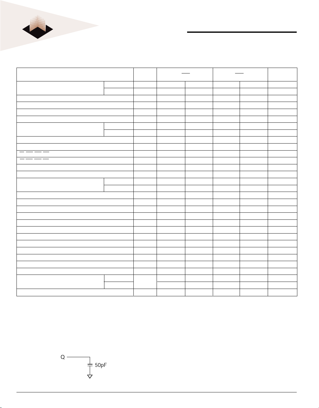
4. Outputs measured at 1.5V with equivalent load:
CL = 3 tAC 76ns
CL = 2 tAC 76ns
CL = 3 tCK 10 8 ns
CL = 2 tCK 13 10 ns
CL = 3 (7) tHZ 76ns
CL = 2 (7) tHZ 76ns
(11)
SymbolSymbol
Symbol
SymbolSymbol
N
1 CLK + 7ns 1 CLK + 7ns —
t
WR
XSR 80 78 ns
5. AC timing and ICC tests have VIL = 0V and VIH = 3V, with timing referenced to
1.5V crossover point.
6. The clock frequency must remain constant (stable clock is defined as a signal
cycling within timing constraints specified for the clock pin) during access or
precharge states (READ, WRITE, including tWR, and PRECHARGE commands). CKE
may be used to reduce the data rate.
7. tHZ defines the time at which the output achieves the open circuit condition;
it is not a reference to VOH or VOL. The last valid data element will meet tOH
before going High-Z.
8. Guaranteed by design, but not tested.
9. AC characteristics assume tT = 1ns.
10. Auto precharge mode only. The precharge timing budget (tRP) begins 7.5ns/
7ns after the first clock delay, after the last WRITE is executed.
11. Precharge mode only.
-100-100
-100
-100-100
MinMin
Min
MinMin
1.8 1.8 ns
15 15 ns
MaxMax
Max
MaxMax
MinMin
Min
MinMin
-125-125
-125
-125-125
MaxMax
Max
MaxMax
UnitUnit
Unit
UnitUnit
1313
13 White Electronic Designs Corporation • (602) 437-1520 • www.whiteedc.com
1313
 Loading...