

Page 1
Service Manual
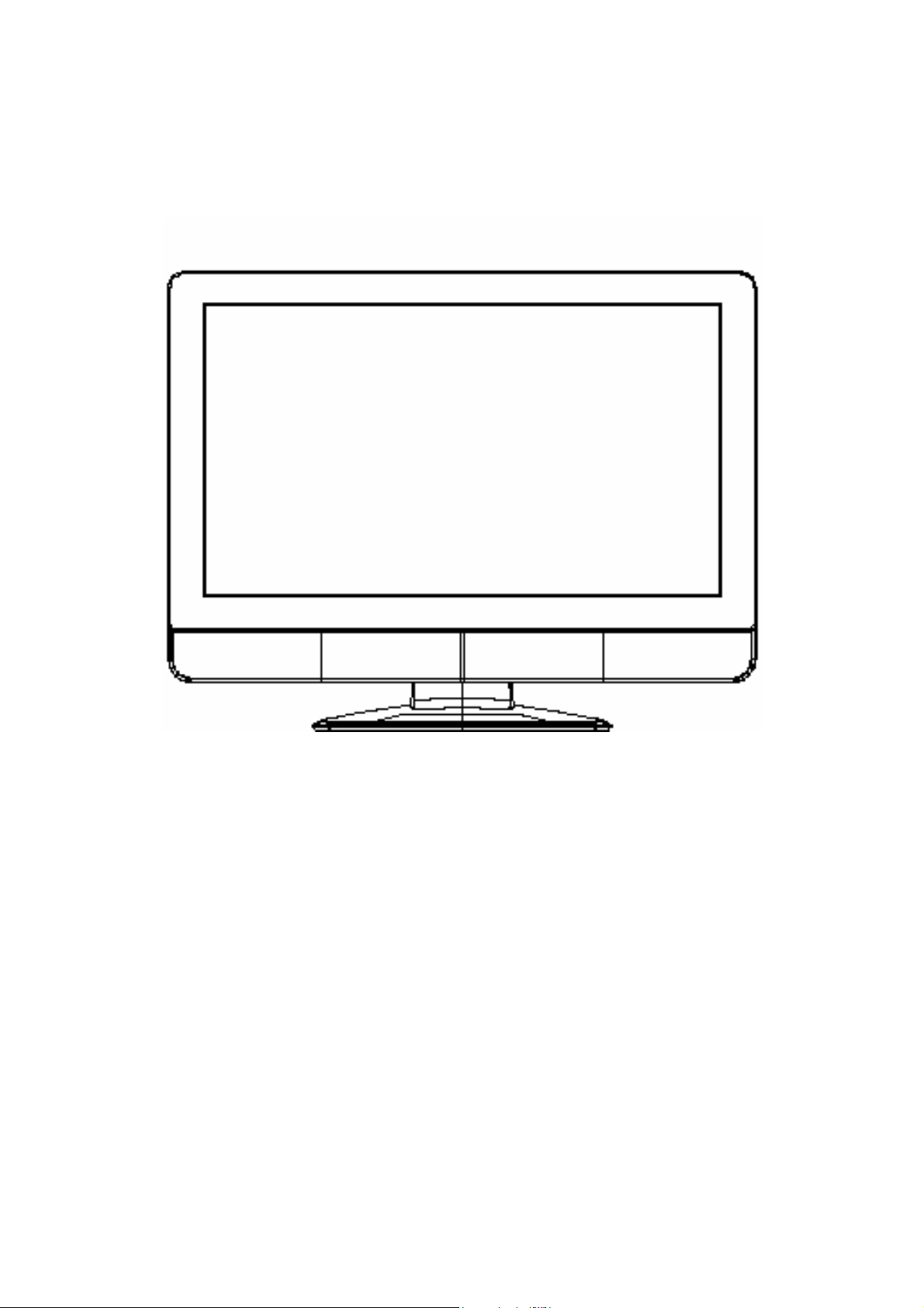
Model #: VIZIO VX37L HDTV10A
V, Inc
320A Kalmus Drive Costa Mesa, CA 92626
TEL : +714-668-0588 FAX :+714-668-9099
Top Confidential
Page 2

Table of Contents
CONTENTS PAGE
Sections
1. Features 1-1
2. Specifications 2-1
3. On Screen Display 3-1
4. Factory Preset Timings
5. Pin Assignment
4-1
5-1
6. Main Board I/O Connections 6-1
7. Theory of Circuit Operation 7-1
8. Waveforms 8-1
9. Trouble Shooting 9-1
10. Block Diagram 10-1
11. Spare parts list 11-1
12. Complete Parts List 12-1
Appendix
1. Main Board Circuit Diagram
2. Main Board PCB Layout
3. Assembly Explosion Drawing
Block Diagram
VIZIO VX37L HDTV10A Service Manual
Page 3

VINC Service Manual
VIZIO VX37L HDTV10A
COPYRIGHT © 2000 V, INC. ALL RIGHTS RESERVED.
IBM and IBM products are registered trademarks of International Business Machines
Corporation.
Macintosh and Power Macintosh are registered trademarks of Apple Computer, Inc.
VINC and VINC products are registered trademarks of V, Inc.
VESA, EDID, DPMS and DDC are registered trademarks of Video Electronics Standards
Association (VESA).
Energy Star is a registered trademark of the US Environmental Protection Agency (EPA).
No part of this document may be copied, reproduced or transmitted by any means for any
purpose without prior written permission from VINC.
FCC INFORMATION
This equipment has been tested and found to comply with the limits of a Class B digital device,
pursuant to part 15 of the FCC Rules. These limits are designed to provide reasonable
protection against harmful interference in a residential installation. This equipment generates,
uses and can radiate radio frequency energy, and if not installed and used in accordance with
the instructions, may cause harmful interference to radio communications. However, there is
no guarantee that the interference will not occur in a particular installation. If this equipment
does cause unacceptable interference to radio or television reception, which can be
determined by turning the equipment off and on, the user is encouraged to try to correct the
interference by one or more of the following measures -- reorient or relocate the receiving
antenna; increase the separation between equipment and receiver; or connect the into an
outlet on a circuit different from that to which the receiver is connected.
FCC WARNING
To assure continued FCC compliance, the user must use a grounded power supply cord and
the provided shielded video interface cable with bonded ferrite cores. Also, any unauthorized
changes or modifications to Amtrak products will void the user’s authority to operate this
device. Thus VINC Will not be held responsible for the product and its safety.
CE CERTIFICATION
This device complies with the requirements of the EEC directive 89/336/EEC with regard to
“Electromagnetic compatibility.”
SAFETY CAUTION
Use a power cable that is properly grounded. Always use the AC cords as follows – USA (UL);
Canada (CSA); Germany (VDE); Switzerland (SEV); Britain (BASEC/BS); Japan (Electric
Appliance Control Act); or an AC cord that meets the local safety standards.
VIZIO VX37L HDTV10A Service Manual
Page 4

Chapter 1 Features
1. Built in TV channel selector for TV viewing.
2. Simulatnueous display of PC and TV images.
3. Connectable to PC’s analog RGB port.
4. Built in S-video, HDTV, composite video, HDMI and TV out.
5. Built in auto adjust function for automatic adjument of screen display.
6. Smoothing function enables display of smooth texts and graphics even if image
withresolution lower than 1366x768 is magnified.
7. Advanced video functions for personal favor.
8. Picture In Picture (PIP) funtion to show TV or VCR images.
9. Power saving to reduce consumption power too less than 3W.
10. On Screen Display: user can define display mode (i.e. color, brightness, contrast,
sharpness, backlight), sound setting, PIP, TV channel program, aspect and
gamma or reset all setting.
CONFIDENTIAL – DO NOT COPY Page 1-1
File No. SG-0209
Page 5

Chapter 2 Specification
1. TFT-LCD CHARACTERISTICS
Model Name: LPL LC370WX1-SLA1 (Vendor: LG. Philips LCD Co., Ltd)
Size: 3702inch
Display Size: 37.02 inches (940.3mm) diagonal
Outline Dimension: 877.0 mm (H) x 516.8 mm (V) x 55.5 mm (D) (Typ.)
Pixel Pitch: 0.200mm x 0.600mm x RGB
Pixel Format: 1366 horiz. By 768 vert. Pixels RGB strip arrangement
Display Operating Mode: Transmissive mode, normally Black
Surface Treatment: Hard Coating (3H) ,Anti-glare treatment of the front polarizer.
2. TFT-LCD OPTICAL CHARACTERISTICS
Contrast ratio: 1.CR : 1400(Typ) 2. CR WITH AI : 2000(Typ)
Surface Luminance, White: 500 cd/m2 (Typ)
Luminance Variation, δ=1.3 (Max)
Response Time = 6 mx (Max=10mx)
Viewing Angle (CR>10)
Left: 89°typ.
Right: 89°typ.
Top: 89°typ.
Bottom: 89°typ.
3. Input Connectors
RJ11, D-SUB15PIN (MINI, 3rows), Headphone, HDMIX2, RCAX3 (component),
RCAX2 (AUDIO in), RCAX3 (composite), RCAX2 (AUDIO in), S-Video, Tuner
4. POWER SUPPLY
Input Voltage Level: 90~240 Vac, 50/ 60 Hz
Power Consumption: 280W MAX
Power OFF: to less than 3W MAX
5. Speaker
Output 10W (max) X2
CONFIDENTIAL – DO NOT COPY Page 2-1
File No. SG-0209
Page 6

6. ENVIRONMENT
Operating Temperature: 5c~35c (Ambient)
Operating Humidity: Ta= 35 °C, 90%RH (Non-condensing)
Operating Altitude: 0 - 14,000 feet (4267.2m)(Non-Operating)
7. DIMENSIONS (Physical dimension)
Width: 800 mm. +/- 20 mm
Depth: 1060 mm +/- 20 mm
Height: 360 mm
+/- 20 mm
8. WEIGHT (Physical weight)
Net: 19.1+/-0.5kgs
Gross: 24.6+/-0.5kgs
Precaution
Please pay attention to the followings when you use this TFT LCD module.
1. OPERATING PRECAUTIONS
(1) The spike noise causes the mis-operation of circuits. It should be lower than
following voltage :
V=±200mV(Over and under shoot voltage)
(2) Response time depends on the temperature. (In lower temperature, it becomes
longer).
(3) Brightness depends on the temperature. (In lower temperature, it becomes
lower.)And in lower temperature, response time (required time that brightness is
stable after turned on) becomes longer.
(4) Be careful for condensation at sudden temperature change. Condensation makes
damage to polarizer or electrical contacted parts. And after fading condensation,
smear or spot will occur.
(5) When fixed patterns are displayed for a long time, remnant image is likely to occur.
(6) Module has high frequency circuits. System manufacturers shall do sufficient
suppression to the electromagnetic interference. Grounding and shielding methods
may be important to minimize the interference.
CONFIDENTIAL – DO NOT COPY Page 2-1
File No. SG-0209
Page 7

2. HANDLING PRECAUTIONS FOR PROTECTION
(1) The protection film is attached to the bezel with a small masking tape. When the
protection film is peeled off, static electricity is generated between the film and
polarizer. This should be peeled off slowly and carefully by people who are
electrically grounded and with well ion-blown equipment or in such a condition, etc.
(2) When the module with protection film attached is stored for a long time, sometimes
there remains a very small amount of glue still on the bezel after the protection film
is peeled off.
(3) You can remove the glue easily. When the glue remains on the bezel surface or its
vestige is recognized, please wipe them off with absorbent cotton waste or other
soft material like chamois soaked with normal-hexane.
CONFIDENTIAL – DO NOT COPY Page 2-1
File No. SG-0209
Page 8

Chapter 3 On Screen Display
On Screen Display (OSD) is a friendly interface providing the function adjusting in our system.
Customers could operate it only by few buttons. There is the introduction of the OSD.
Main unit button
MENU OK
CH ▲ ↑
CH ▼ ↓
VOL + ←
VOL - →
Input
[MENU]
“MENU” button could star the OSD which could adjust the performance and set up the setting
between the different input sources. There are the structures.
TV Source
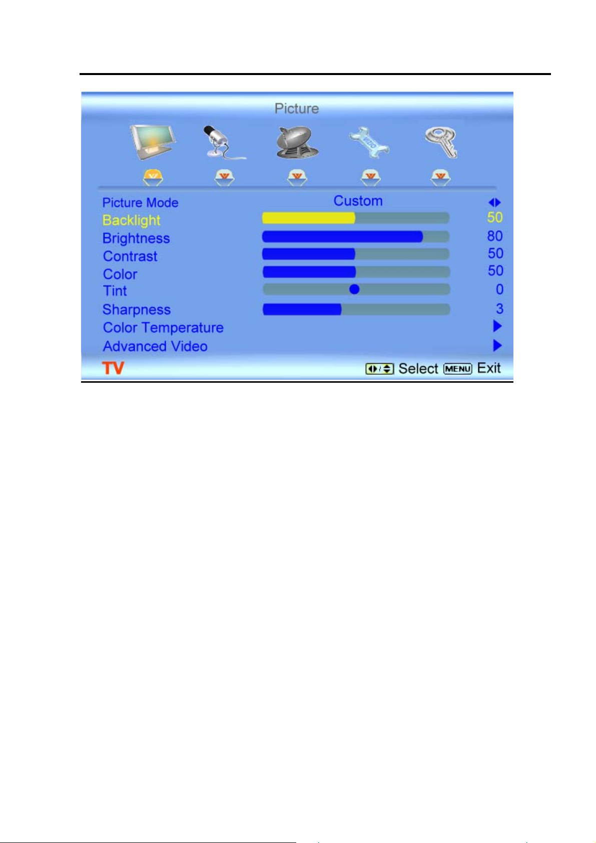
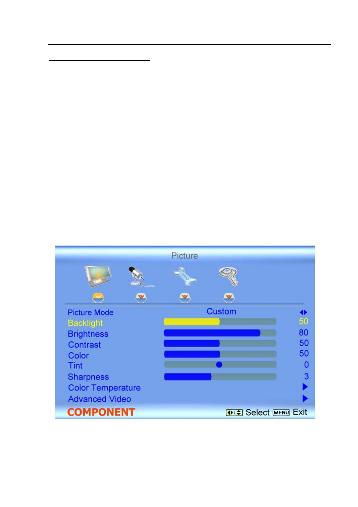
A. Picture:(Bold: Default)
a. Picture Mode (Standard/Movie /Game / Custom)
b. Backlight (0~100, 90)
c. Contrast (0~100, 50)
d. Brightness (0~100, 50)
e. Color (saturation)(0~100, 50)
f. Tint (hue) (-32~32, 0)
g. Sharpness (0~7, 4)
h. Color Temperature (Cool/Normal/Warm/Custom)
i. Advanced Video
1. DNC (Low/Medium/Strong/Off)
2. Black level extender (Off/On)
3. White Peak Limiter (On/Off)
4. CTI (Low/Medium/Strong/Off)
5. Flesh Tone (Off/On)
6. Adaptive Luma (Off/On)
CONFIDENTIAL – DO NOT COPY Page 3-1
File No. SG-0209
Page 9
CONFIDENTIAL – DO NOT COPY Page 3-2
File No. SG-0209
Page 10
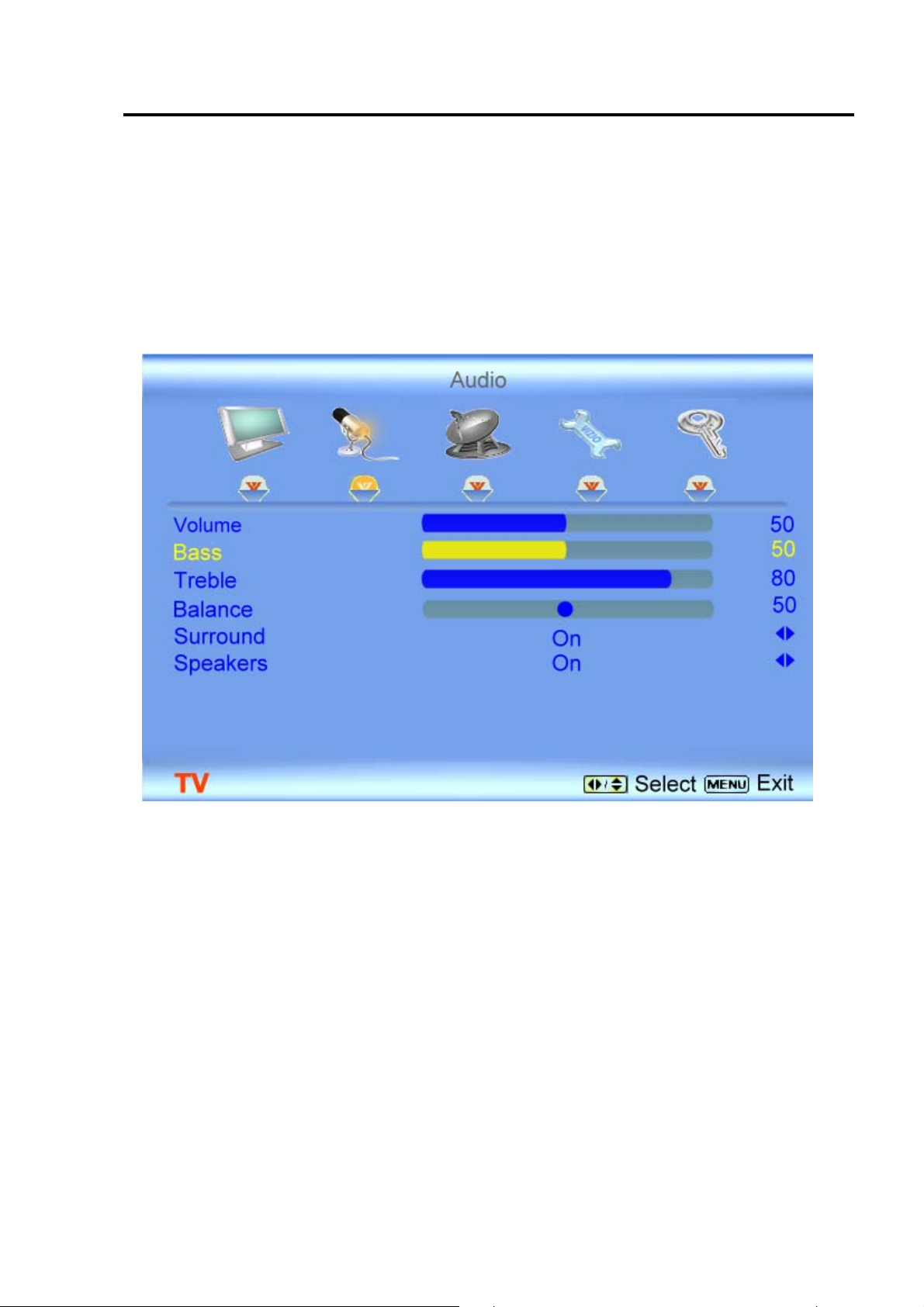
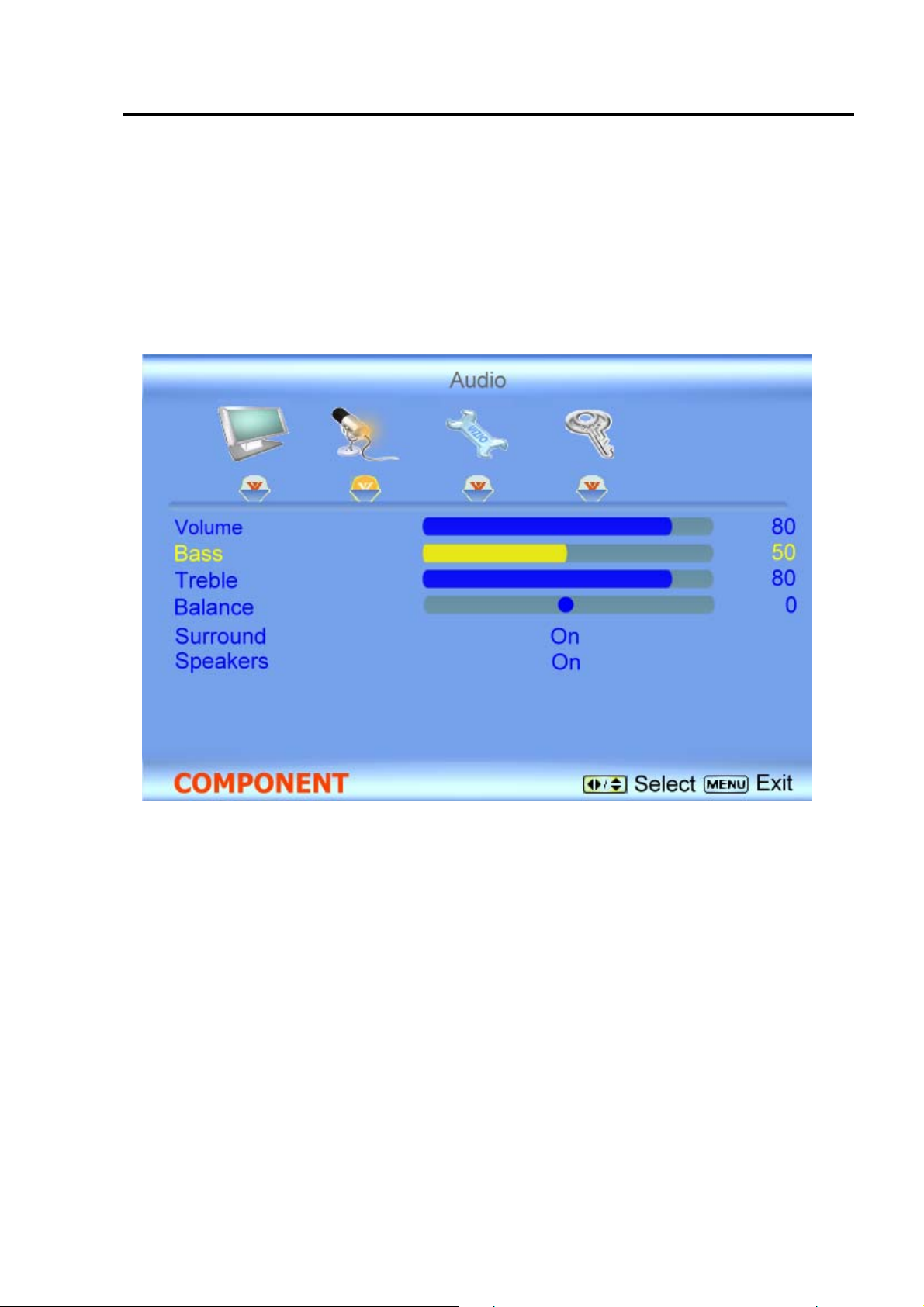
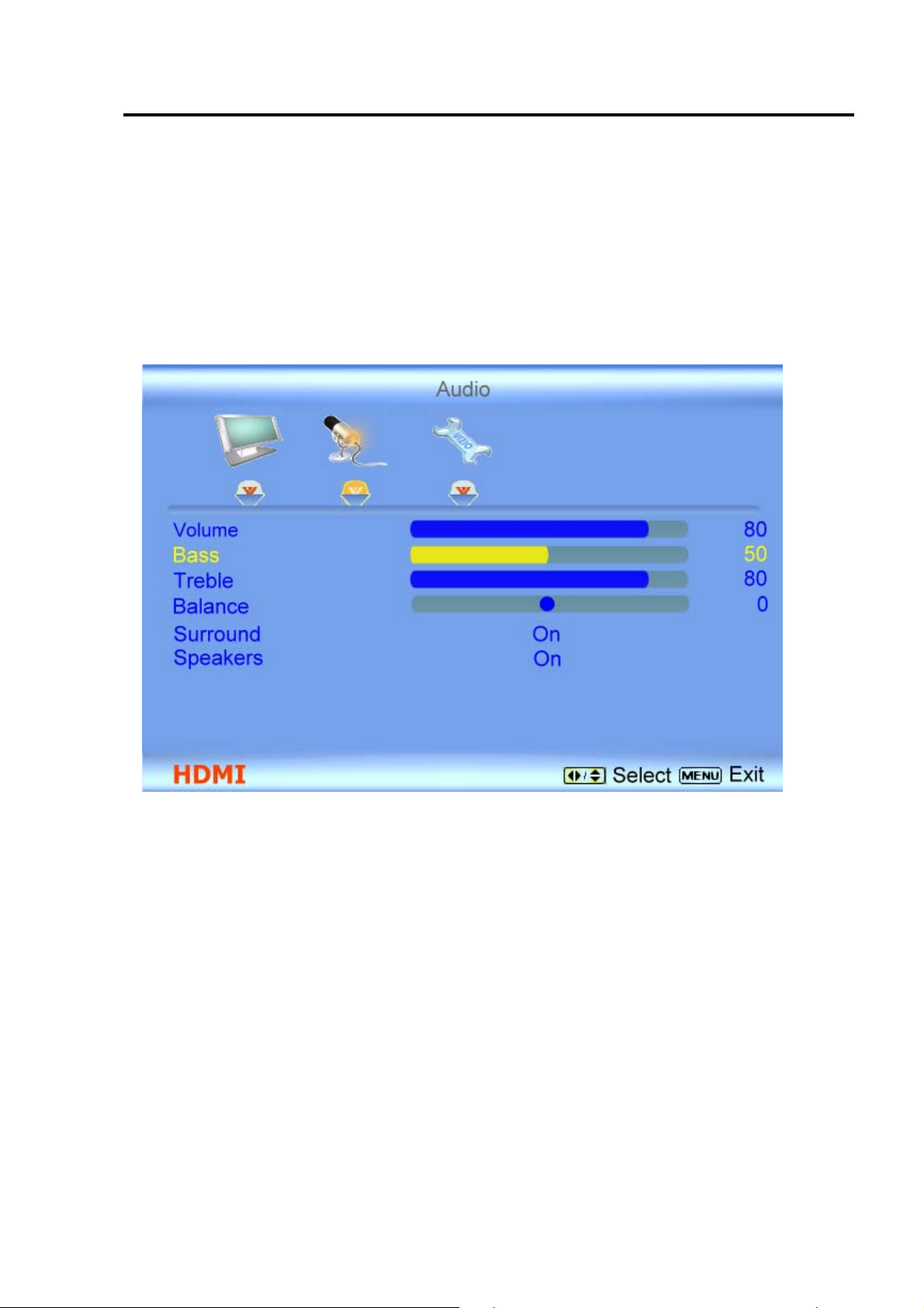
B. Audio:(Bold: Default)
a. Volume (0~100, 25)
b. Bass (0~100, 50)
c. Treble (0~100, 50)
d. Balance (-50~50, 0)
e. Surround (ON/OFF)
f. Speakers (ON/OFF)
CONFIDENTIAL – DO NOT COPY Page 3-3
File No. SG-0209
Page 11
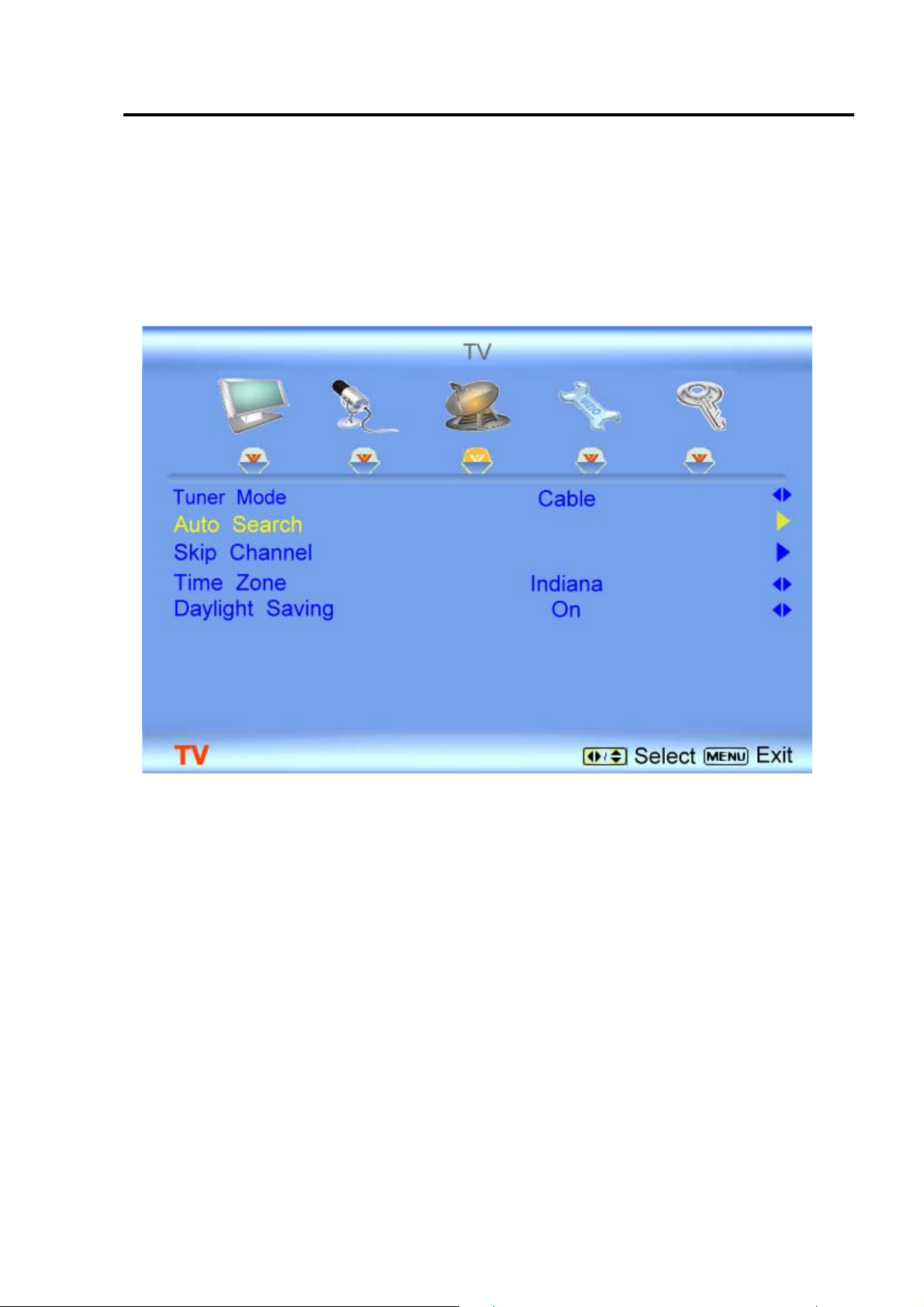
C. TV:(Bold: Default)
a. Tuner Mode (Cable/Air)
b. Auto Search
c. Skip Channel
d. Digital Audio Out (PCM/Dolby Digital/OFF)
e. Time Zone (Eastern/Indiana/Central/Mountain/Arizona/Pacific/Alaska/Hawaii)
CONFIDENTIAL – DO NOT COPY Page 3-4
File No. SG-0209
Page 12
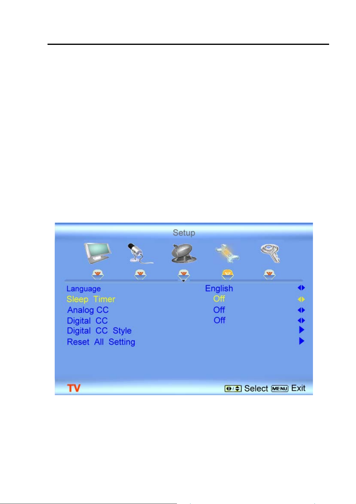
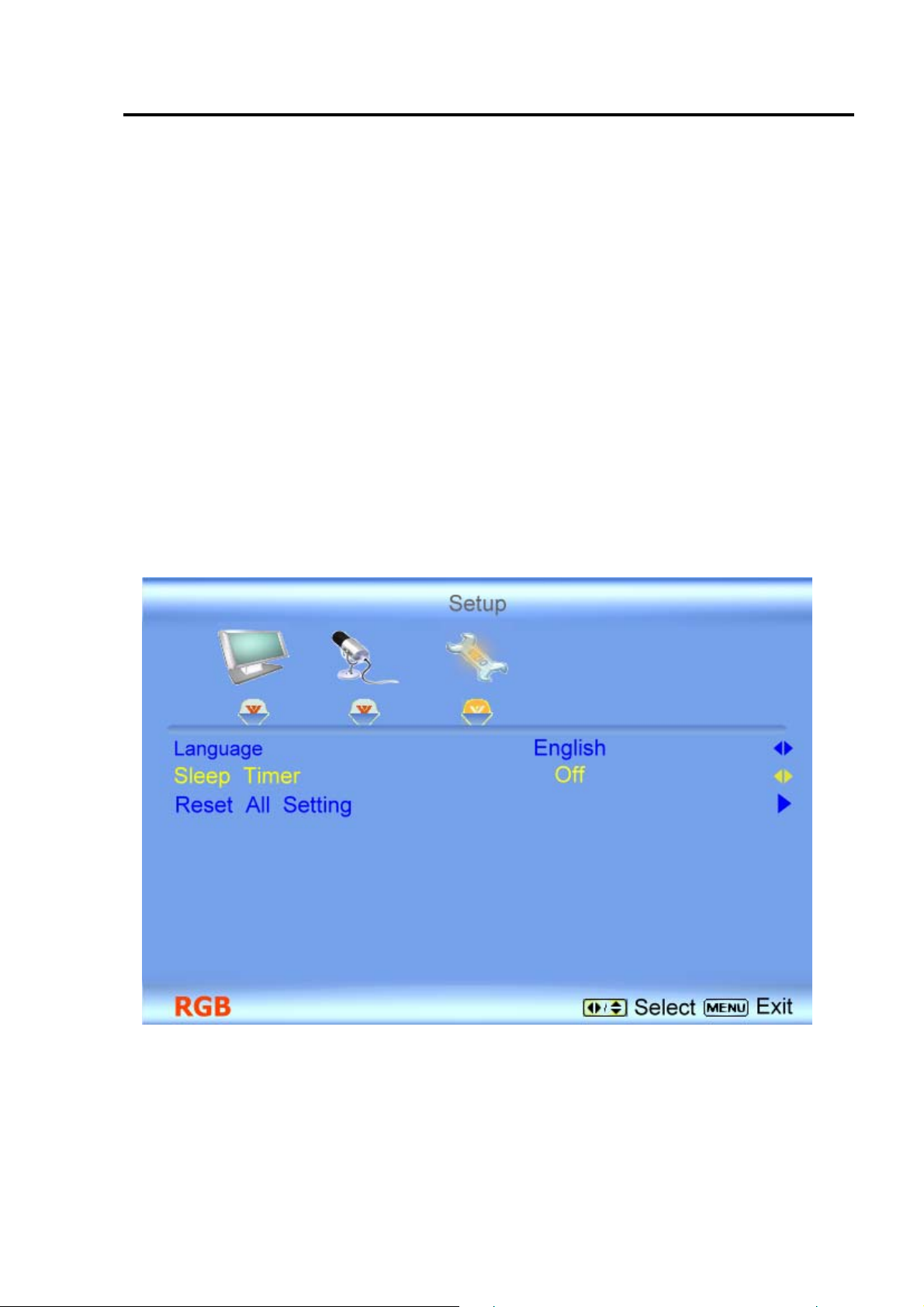
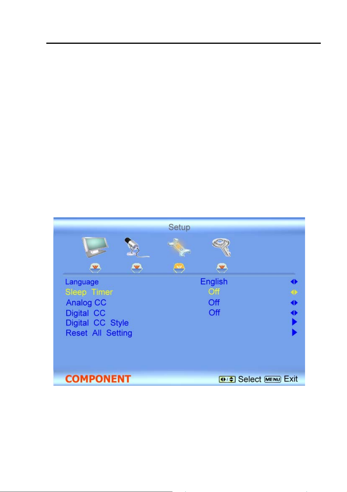
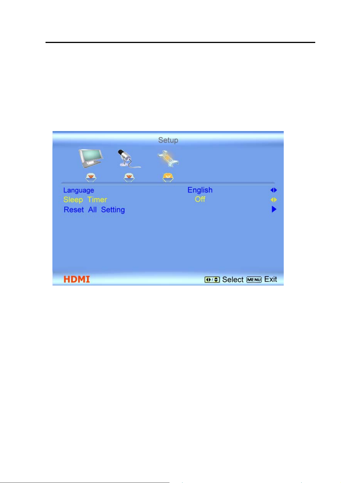
D. Setup:(Bold: Default)
a. Language (English/ Français / Espaňol)
b. Sleep Timer (OFF/30Min/60Min/90Min/120Min)
c. Analog CC (OFF/CC1~4/TT1~4)
d. Digital CC (OFF/CC1~4/Service1~6)
e. Digital CC Style
1. Caption Style (As Broadcaster/Custom)
2. Size (Large/Small/Medium)
3. Font Color (White/Green/Blue/Red/Cyan/Yellow/Magenta/Black)
4. Font Opacity (Solid/Translucent/Transparent)
5. Background Color (White/Green/Blue/Red/Cyan/Yellow/Magenta/Black)
6. Background Opacity (Solid/Translucent/Transparent)
7. Window Color (White/Green/Blue/Red/Cyan/Yellow/Magenta/Black)
8. Window Opacity (Solid/Translucent/Transparent)
g. Rest All Setting (OK/Cancel)
CONFIDENTIAL – DO NOT COPY Page 3-5
File No. SG-0209
Page 13
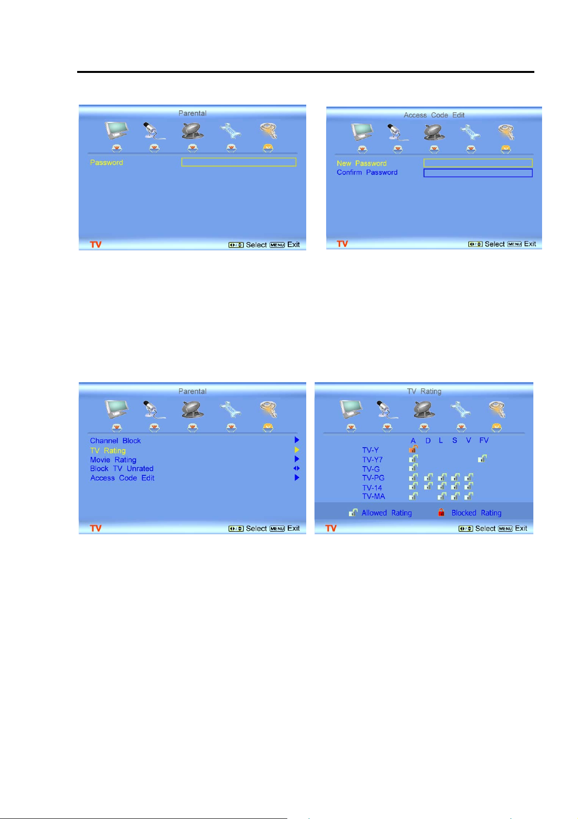
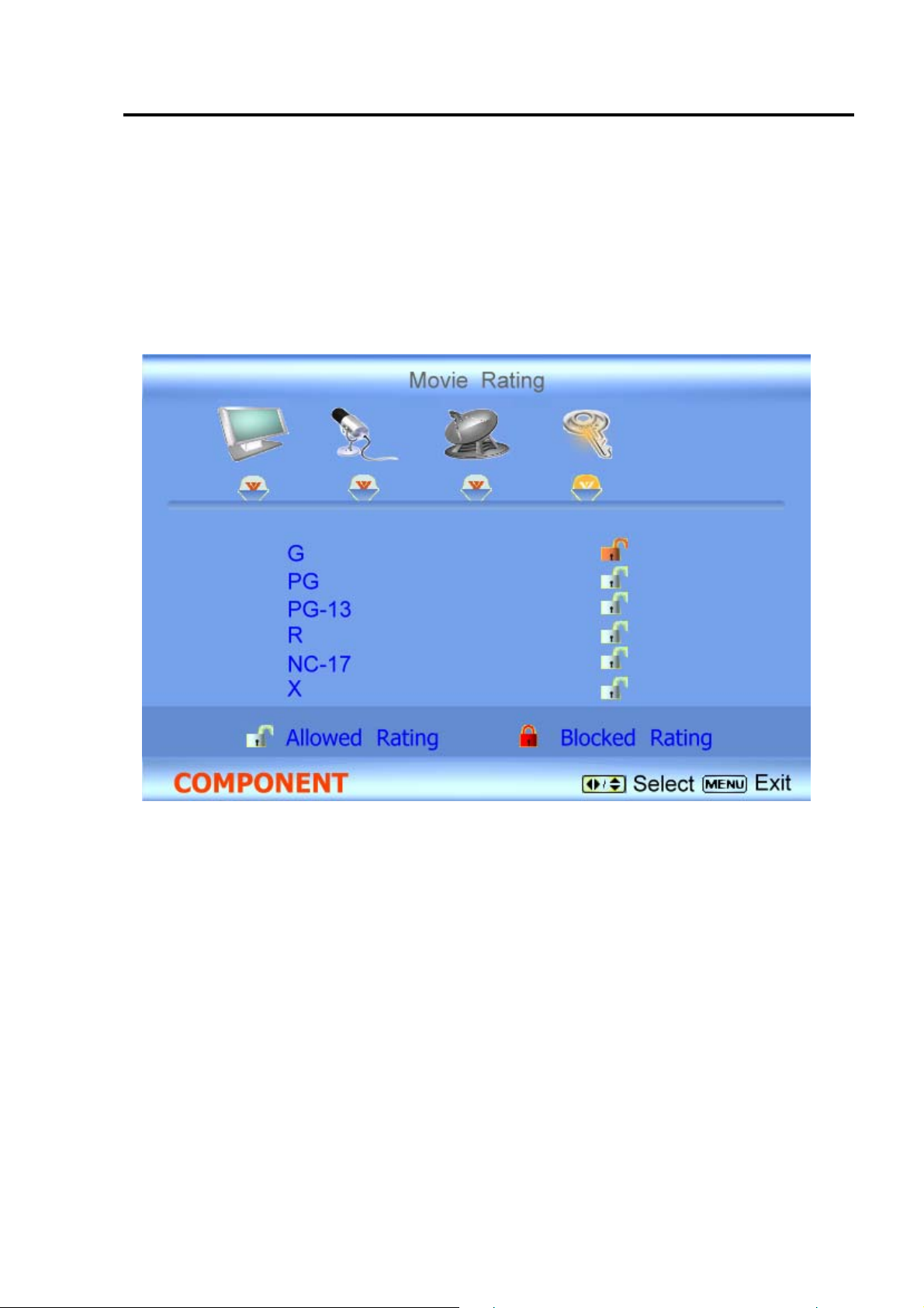
E. Parental:(Bold: Default)
Password (Default => 0000)
a. Cannel Block
b. TV Rating
c. Move Rating
d. Block Unrated TV (NO/Yes)
e. Access Code Edit
CONFIDENTIAL – DO NOT COPY Page 3-6
File No. SG-0209
Page 14
RGB Mode
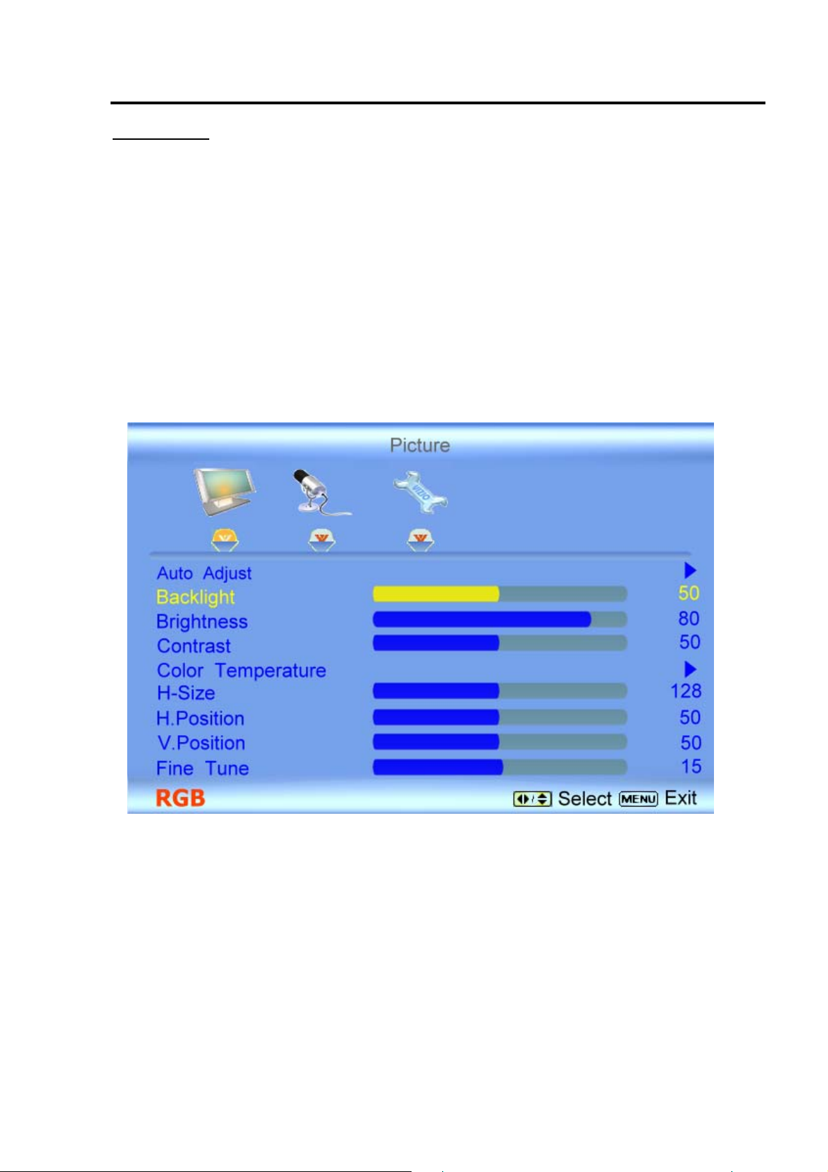
A. Picture Adjust:(Bold: Default)
a. Auto Adjust
b. Backlight (0~100, 90)
c. Contrast (0~100, 50)
d. Brightness (0~100, 50)
e. Color Temperature (6500/9300/Custom)
f. H-Size (0~255, 127)
g. H-Position (0~100, 65)
h. V-Position (0~100, 49)
i. Fine Tune (0~31, 17)
CONFIDENTIAL – DO NOT COPY Page 3-7
File No. SG-0209
Page 15
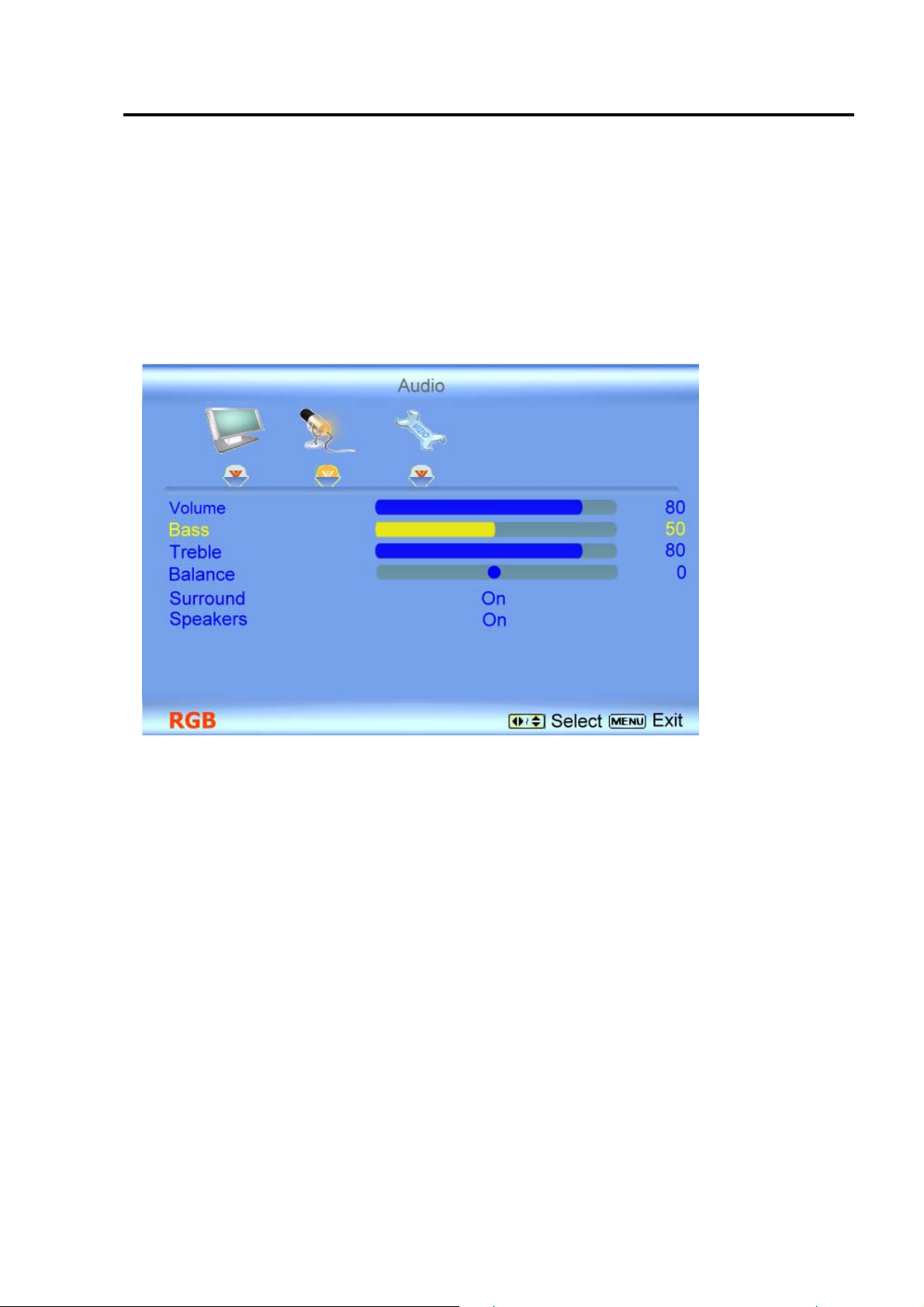
B. Audio:(Bold: Default)
a. Volume (0~100, 25)
b. Bass (0~100, 50)
c. Treble (0~100, 50)
d. Balance (-50~50, 0)
e. Surround (ON/OFF)
f. Speakers (ON/OFF)
CONFIDENTIAL – DO NOT COPY Page 3-8
File No. SG-0209
Page 16
C. Setup:(Bold: Default)
a. Language (English/ Français / Espaňol)
b. Sleep Timer (OFF/30Min/60Min/90Min/120Min)
c. Analog CC (OFF/CC1~4/TT1~4)
d. Digital CC (OFF/CC1~4/Service1~6)
e. Digital CC Style
1. Caption Style (As Broadcaster/Custom)
2. Size (Large/Small/Medium)
3. Font Color (White/Green/Blue/Red/Cyan/Yellow/Magenta/Black)
4. Font Opacity (Solid/Translucent/Transparent)
5. Background Color (White/Green/Blue/Red/Cyan/Yellow/Magenta/Black)
6. Background Opacity (Solid/Translucent/Transparent)
7. Window Color (White/Green/Blue/Red/Cyan/Yellow/Magenta/Black)
8. Window Opacity (Solid/Translucent/Transparent)
g. Rest All Setting (OK/Cancel)
CONFIDENTIAL – DO NOT COPY Page 3-9
File No. SG-0209
Page 17
AV / COMPONENT MODE
A. Picture:(Bold: Default)
a. Picture Mode (Standard/Movie /Game / Custom)
b. Backlight (0~100, 90)
c. Contrast (0~100, 50)
d. Brightness (0~100, 50)
e. Color (saturation)(0~100, 50)
f. Tint (hue) (-32~32, 0)
g. Sharpness (0~7, 4)
h. Color Temperature (Cool/Normal/Warm/Custom)
i. Advanced Video
1. DNC (Low/Medium/Strong/Off)
2. Black level extender (Off/On)
3. White Peak Limiter (On/Off)
4. CTI (Low/Medium/Strong/Off)
5. Flesh Tone (Off/On)
6. Adaptive Luma (Off/On)
CONFIDENTIAL – DO NOT COPY Page 3-10
File No. SG-0209
Page 18
B. Audio:(Bold: Default)
a. Volume (0~100, 25)
b. Bass (0~100, 50)
c. Treble (0~100, 50)
d. Balance (-50~50, 0)
e. Surround (ON/OFF)
f. Speakers (ON/OFF)
CONFIDENTIAL – DO NOT COPY Page 3-11
File No. SG-0209
Page 19
C. Setup:(Bold: Default)
a. Language (English/ Français / Espaňol)
b. Sleep Timer (OFF/30Min/60Min/90Min/120Min)
c. Analog CC (OFF/CC1~4/TT1~4)
d. Digital CC (OFF/CC1~4/Service1~6)
e. Digital CC Style
1. Caption Style (As Broadcaster/Custom)
2. Size (Large/Small/Medium)
3. Font Color (White/Green/Blue/Red/Cyan/Yellow/Magenta/Black)
4. Font Opacity (Solid/Translucent/Transparent)
5. Background Color (White/Green/Blue/Red/Cyan/Yellow/Magenta/Black)
6. Background Opacity (Solid/Translucent/Transparent)
7. Window Color (White/Green/Blue/Red/Cyan/Yellow/Magenta/Black)
8. Window Opacity (Solid/Translucent/Transparent)
g. Rest All Setting (OK/Cancel)
CONFIDENTIAL – DO NOT COPY Page 3-12
File No. SG-0209
Page 20
D. Parental:(Bold: Default)
Password (Default => 0000)
a. Cannel Block
b. TV Rating
c. Move Rating
d. Block Unrated TV (NO/Yes)
e. Access Code Edit
CONFIDENTIAL – DO NOT COPY Page 3-13
File No. SG-0209
Page 21

HDMI MODE
A. Picture:(Bold: Default)
a. Picture Mode (Standard/Movie /Game / Custom)
b. Backlight (0~100, 90)
c. Contrast (0~100, 50)
d. Brightness (0~100, 50)
e. Color (saturation)(0~100, 50)
f. Tint (hue) (-32~32, 0)
g. Sharpness (0~7, 4)
h. Color Temperature (Cool/Normal/Warm/Custom)
i. Advanced Video
1. DNC (Low/Medium/Strong/Off)
2. Black level extender (Off/On)
3. White Peak Limiter (On/Off)
4. CTI (Low/Medium/Strong/Off)
5. Flesh Tone (Off/On)
6. Adaptive Luma (Off/On)
CONFIDENTIAL – DO NOT COPY Page 3-14
File No. SG-0209
Page 22
B. Audio:(Bold: Default)
a. Volume (0~100, 25)
b. Bass (0~100, 50)
c. Treble (0~100, 50)
d. Balance (-50~50, 0)
e. Surround (ON/OFF)
f. Speakers (ON/OFF)
CONFIDENTIAL – DO NOT COPY Page 3-15
File No. SG-0209
Page 23
C. Setup:(Bold: Default)
a. Language (English/ Français / Espaňol)
b. Sleep Timer (OFF/30Min/60Min/90Min/120Min)
c. Analog CC (OFF/CC1~4/TT1~4)
d. Digital CC (OFF/CC1~4/Service1~6)
e. Digital CC Style
g. Rest All Setting (OK/Cancel)
CONFIDENTIAL – DO NOT COPY Page 3-16
File No. SG-0209
Page 24
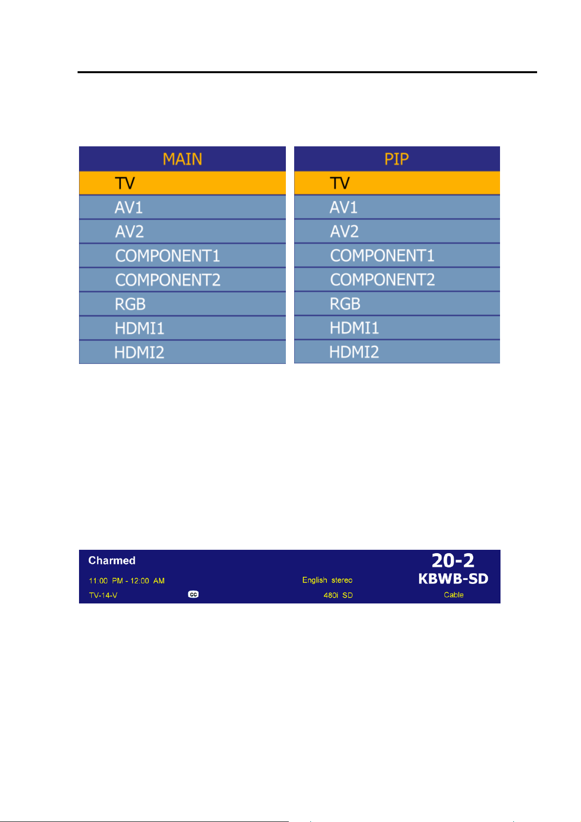
[INPUT]
“INPUT” could supply an interface providing a list. The list shows input sources and
provides the choices of different sources. The list includes items as below:
A. TV: Analog TV or digital TV
B. AV1, AV2: Composite (AV) signal
C. Component1, Component2: Color difference (YPbPr) video signals.
D. RGB: Video Graphics Array (VGA) or D-sub video signals.
E. HDMI1, HDMI2: High Definition Multimedia Interface (HDMI) multimedia signals.
Note: The list of PIP provides the choices of different sources on sub-screen.
[INFO]
“INFO” button could show an information bar which displays the information about the
input signal on our LCD TV.
CONFIDENTIAL – DO NOT COPY Page 3-17
File No. SG-0209
Page 25
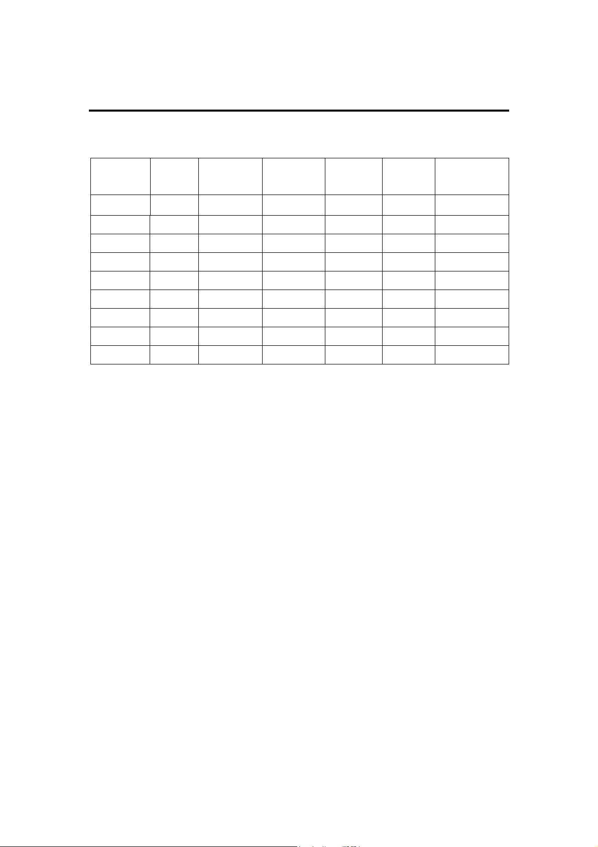
Chapter4 Factory preset timings
This timing chart is already preset for the TFT LCD analog & digital display
monitors.
Resolution
Refresh
rate
640x480 60Hz 31.5kHz 59.94Hz N N 25.175
640x480 75Hz 37.5kHz 75.00Hz N N 31.500
800X600 60Hz 37.9kHz 60.317Hz P P 40.000
800x600 75Hz 46.9kHz 75.00Hz P P 49.500
800X600 85Hz 53.7kHz 85.06Hz P P 56.250
1024x768 60Hz 48.4kHz 60.01Hz N N 65.000
1024X768 75Hz 60.0kHz 75.03Hz P P 78.750
720x400 70Hz 31.46kHz 70.08Hz N P 28.320
1366X768 60 47.7KHZ 60.00HZ P N 85.500
Remark: P: positive N: negative
Horizontal
Frequency
Vertical
Frequency
Horizontal
Polarity
Vertical
Polarity
Pixel
Rate
CONFIDENTIAL – DO NOT COPY Page 4-1
File No. SG-0209
Page 26
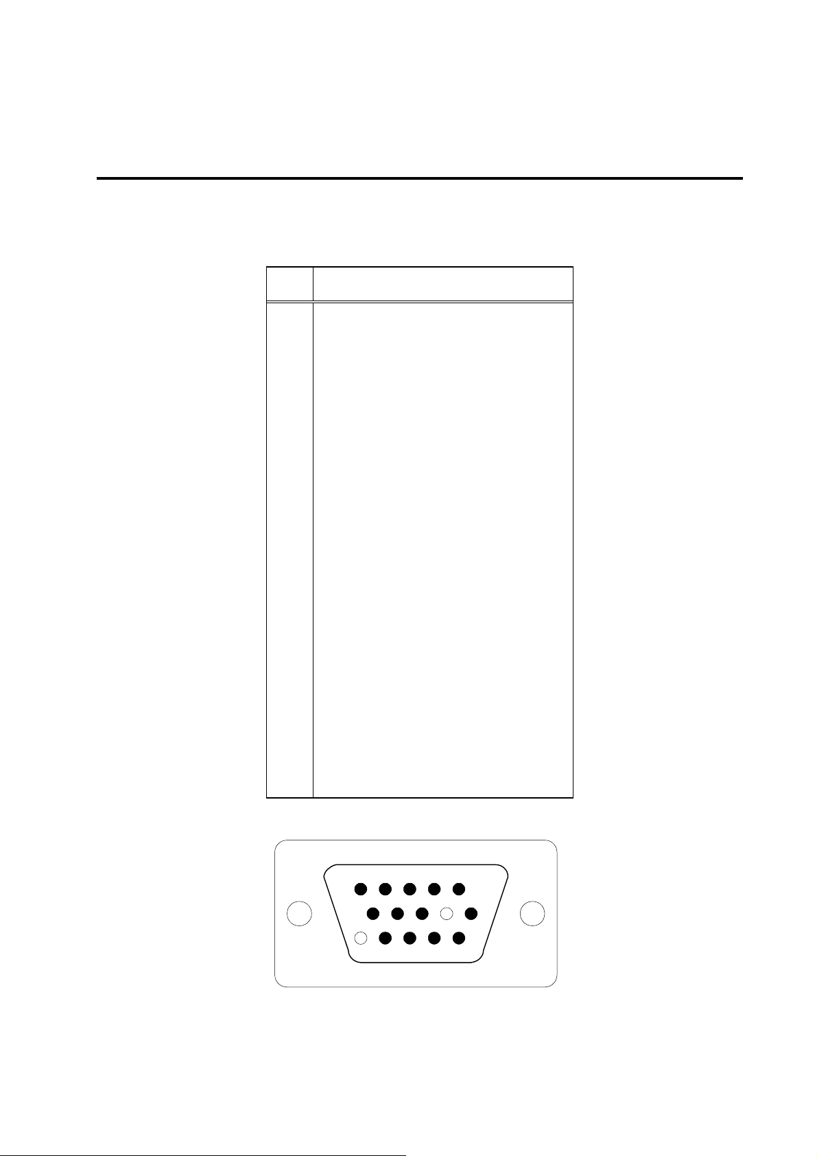
Chapter5 Connectors Pin Assignment &
Signal Specification
Video Graphics Array (VGA) connector pin assignment
The TFT LCD analog display monitors use a 15 Pin Mini D-Sub connector as video input
source.
Pin Description
1 Red
2 Green
3 Blue
4 Ground
5 Ground
6 R-Ground
7 G-Ground
8 B-Ground
9 +5V for DDC
10 Ground
11 No Connection
12 (SDA)
13 H-Sync (Composite Sync)
14 V-Sync
15 (SCL)
1
5
106
CONFIDENTIAL – DO NOT COPY
11
15
Page 5-1
File No. SG-0209
Page 27
High Definition Multimedia Interface (HDMI) connector pin assignment
PIN SIGNAL ASSIGNMENT
1 TMDS Data2+
2 TMDS Data2 Shield
3 TMDS Data2-
4 TMDS Data1+
5 TMDS Data1 Shield
6 TMDS Data1-
7 TMDS Data0+
8 TMDS Data0 Shield
9 TMDS Data0-
10 TMDS Clock+
11 TMDS Clock Shield
12 TMDS Clock-
13 CEC
14 Reserved (N.C on device)
15 SCL
16 SDA
17 DDC/CEC Ground
18 +5V Power
19 Hot Plug Detect
CONFIDENTIAL – DO NOT COPY
Page 5-2
File No. SG-0209
Page 28
Four-Pin mini DIN S-Video Connector pin assignment
1, 2 = GND
3 = Luminance (Y)
4 = Chrominance(C)
Signal Specification
F-Type TV RF connector
a. Signal Level 60dBµV typical
b. System: NTSC
c. Frequency: 55~801MHz (NTSC)
PC connector 15 pin male D-sub connector
a. Pin Assignment Refer to Section 2.3.10
b. Signal Level Video (R, G, B): Analog 0.7Vp-p/75
Sync (H, V): TTL level
c. Sync Type TTL (Separate / Composite) or Sync. On Green
d. Sync polarity Positive or Negative
e. Video Amplitude RGB: 0.7Vp-p
f. Frequency H: support to 30K~70KHz
V: support to 50~85Hz
Pixel Clock: support to 110MHz
CONFIDENTIAL – DO NOT COPY
Page 5-3
File No. SG-0209
Page 29

Four-Pin mini DIN S-Video
a. Pin Assignment refer to S-Video connector pin assignment
b. Signal Level Video (Y): Analog 0.1Vp-p/75
Video (C): Analog 0.286p-p/75
Sync (H+V): 0.3V below Video (Y)
c. Frequency H: 15.734KHz V: 60Hz (NTSC)
Signal Level Video (Y) : Analog 0.1Vp-p/75
Video (C) : Analog 0.286p-p/75
Sync (H+V): 0.3V below Video (Y)
Frequency: H: 15.734Khz V: 60HZ (NTSC)
HDMI Signal:
a. Pin Assignment Refer to HDNI Pin Assignment
b. Type A
c. Polarity Positive or Negative
d. Frequency
H: 15.734KHz V: 60Hz (NTSC-480i)
H: 31KHz V: 60Hz (NTSC-480p)
H: 45KHz V: 60Hz (NTSC-720p)
H: 33KHz V: 60Hz (NTSC-1080i)
Component signal
a. Frequency H: 15.734KHz V: 60Hz (NTSC-480i)
H: 31KHz V: 60Hz (NTSC-480p)
H: 45KHz V: 60Hz (NTSC-720p)
H: 33KHz V: 60Hz (NTSC-1080i)
b. Signal level Y: 1Vp-p Pb: ±0.350Vp-p Pr: ±0.350Vp-p
c. Impedance 75
CONFIDENTIAL – DO NOT COPY
Page 5-4
File No. SG-0209
Page 30
Chapter6 Main Board I/o Connections
J1 CONNECTION [MAIN BD TO POWER BD]
Pin Description
1 “POWRSW”
2 “+12V”
3 “+12V”
4 “+12V”
5 “+12V”
6 “GND”
7 “GND”
8 “GND”
9 “+5V”
10 “+5V”
11 “+5V”
12 “PWM”
13 “BL ON/OFF”
J2 CONNECTION [MAIN BD TO DISPLAY BD ]
Pin Description
1 “BL-RED”
2 “BL-WHITE”
3 “+5V”
4 “+5V”
5 “IR”
6 “GND”
7 “GND”
8 “KEYPAD-ADC1”
9 “KEYPAD-ADC2”
10 “+3.3V”
CONFIDENTIAL – DO NOT COPY Page 6-1
File No. SG-0209
Page 31

J4 CONNECTOR [MAIN BD TO SIDE JACK]
Pin Description
1 “AV1-IN”
2 “GND”
3 “AV1L-IN”
4 “GND”
5 “AV1R-IN”
6 “GND”
7 “SY1-IN”
8 “GND”
9 “SC1-IN”
10 “GND”
11 “SVDET1”
12 “NC”
J6 CONNECTOR [MAIN BD TO SPEAKER]
Pin Description
1 “R+”
2 “R-”
3 “L-”
4 “L+”
CONFIDENTIAL – DO NOT COPY Page 6-2
File No. SG-0209
Page 32

Chapter 7 Theory of Circuit Operation
The route of D-SUB 15pin input
An RGB (analog) signal is inputted the D-SUB 15pin to the MT5372 which transfers it to a digital
signal by the A/D converter. Then MT5372 generates a Low Voltage Differential Signal (LVDS) for
display device.
The route of HDMI CON input
A HDMI (digital) signal is inputted the HDMI 1&2 CON to the PI3HDMI412FT switch. The passing
signal is processed with the MT5372. Then MT5372 generates a LVDS for display device.
The route of HDTV & Component input
HDTV & Component signal is inputted to the MT5372. After processing, MT5372 generates a
LVDS for display device. The audio signal is inputted WM8776
transmits the signal to TDA8946J
signal.
, an audio amplifier. Then, the amplified signal is the output audio
. After processing, WM8776
The route of Video 1,2,3 & S-Video input
The Video 1,2 and S-Video signal is inputted to the MT5372.After processing, MT5372 generates a
LVDS for display device. The audio signal is inputted WM8776. After processing, WM8776
transmits the signal to TDA8946J, an audio amplifier. Then, the amplified signal is the output audio
signal.
The route of TV input
TV signal is demodulated by the tuner then the demodulating signal is divided into two parts, video
and audio signal. The video signal is processed by MT5372 then MT5372 generates a LVDS for
display device. The audio signal is transmitted in the route named SIF. The SIF signal is
demodulated and decoded by MT5372. The decoded analog signal is transferred into I2S, which is
digital signal, by MT5372. The I2S signal is inputted and transferred into analog signal by WM8776.
After processing, WM8776 transmits the signal to TDA8946J, an audio amplifier. Then, the
amplified signal is the output audio signal.
CONFIDENTIAL – DO NOT COPY Page 7-1
File No. SG-0209
Page 33

The route of DTV input
DTV signal demodulated by the tuner then the demodulating signal is divided into two parts, video
and audio signal. The video signal is decoding by MT5112
MPEG4, is transmitted to and processed by MT5372. Also, MT5372 generates a LVDS for display
device. The audio signal is transmitted in the route named FAT-IN. The FAT-IN signal is
demodulated and decoded by MT5372. The decoded analog signal is transferred into I2S, which is
digital signal, by MT5372. The I2S signal is inputted and transferred into analog signal by WM8776.
After processing, WM8776 transmits the signal to TDA8946J, an audio amplifier. Then, the
amplified signal is the output audio signal.
. The decoded signal, as the format of
The operation of keypad
There are 7 keys to control and to select the function of VX37. Also, there is a LED back light under
the logo “VIZIO” to indicate the status of operation (Orange => STANDBY, White => ON). They are
“Power, ▼▲, + -, Input, MENU”.
MT5372
Ⅰ.GENERAL DESCRIPTION
The MediaTek MT5372 consists of a DTV backend decoder and a TV controller and offers
high integration for advanced applications in main stream integrated digital television
market. The MT5372 combines a transport de-multiplexer, a high definition MPEG-2 video
decoder, an AC3 audio decoder, an LVDS transmitter, and an NTSC/PAL/SECAM video
decoder with a 3D comb filter. The MT5372 enables consumer electronics manufactures
to build high quality, feature-rich DTVs.
World-Leading Video Technology
The MT5372 includes MediaTek’s proprietary de-interlacing technology, the MDDiTM
solution to generate very smooth picture quality for motions. A 3D comb filter added to the
video decoder recovers great detail for still pictures. The special color processing
technology provides natural colors and true studio quality graphics.
Rich Features for High Value Products
Additional features of iDTVs for the MT5372 release are the abilities to support the HDMI
receiver, PIP/POP functionalities, memory cards and DV decoding.
CONFIDENTIAL – DO NOT COPY Page 7-2
File No. SG-0209
Page 34

Reliable Analog Technology
The MT5372 integrates high speed VGA ADC, high resolution Video/Audio ADC, 90db
Audio DACs. The MT5372 provides very fine quality for the iDTV markets.
System Block Diagram
Functional Block Diagram
CONFIDENTIAL – DO NOT COPY Page 7-3
File No. SG-0209
Page 35

Ⅱ. Features of MT5372
1. Key Features:
1. A transport de-multiplexer
2. An MPEG-2 video decoder
3. An AC3 audio decoder
4. A 3D comb TV decoder
5. PIP/POP mode
6. An HDMI receiver
7. A set of three VGA ADCs
2. Host CPU:
1. ARM 926
2. 16K I-Cache and 16K D-Cache
3. 8K Data TCM and 8K Instruction TCM
4. JTAG ICE interface
5. Watch Dog timers
6. Built-in CPI analyzer
3. Transport De-multiplexer:
1. Supports one independent transport stream input
2. Supports serial / parallel interfaces for transport stream input
3. Supports ATSC, DVB, and MPEG2 transport stream inputs
4. Programmable sync detection
5. Supports DES/3-DES/DVB/Multi-2 de-scramblers
6. Up to 8 PIDs even/odd keys for descrambling
7. Supports 32 PID filters and 32 section filters
8. Supports positive/negative/mask section filtering
4. MPEG-2/JPEG Decoder:
1. Supports one MPEG-2 HD decoder
2. MPEG compliant with DV, MP@ML, MP@HL and MPEG-1 video standards
3. JPEG decode base-line or progressive JPEG file
CONFIDENTIAL – DO NOT COPY Page 7-4
File No. SG-0209
Page 36

5. 2D Graphics:
1. Supports multiple color modes
2. Point, horizontal/vertical line primitive drawings
3. Rectangle fill and gradient fill functions
4. Bitblt with transparent, alpha blending, alpha composition and stretch
5. Font rendering by color expansion
6. YCbCr to RGB color space transfer
7. Supports off-line scaler
6. OSD Plane:
1. Three linking list OSD with multiple color modes
2. Two OSD with scaler
3. Square size, 32x32 or 64x64 pixel, hardware cursor
7. Video Plane:
1. Supports clip
2. Flesh tone management
3. Gamma/anti-Gamma correction
4. Color Transient Improvement (CTI)
5. 2D peaking
6. Saturation/hue adjustment
7. Brightness and contrast adjustment
8. Black level extender
9. White peak level limiter
10. Adaptive Luma/Chroma management
11. Automatic detection of films or video sources
12. 3:2/2:2 pull down source detection
13. SD/HD advanced motion adaptive de-interlacing with excellent low angle
14. Arbitrary ratio vertical/horizontal scaling of video, from 1/32X to 32X
15. Advanced linear and non-linear panoramic scaling.
16. Programmable zoom viewer
17. Progressive scan output
18. Supports alpha blending
19. Picture-in-Picture (PIP)
20. Picture-Outside-Picture (POP)
CONFIDENTIAL – DO NOT COPY Page 7-5
File No. SG-0209
Page 37

21. Dithering processing for flat panel display
22. Frame rate conversion, 50Hz to 75Hz
23. Supports mirror and upside down video outputs
24. Supports 480i/ 576i/ 480p /576p/ 720p/ 1080i/ 1080p output forma
8. LVDS:
1. One 10-bit channel or dual 6/8-bit channel
2. Built-in spread spectrum for EMI performance
3. Supports 6/8/10-bit format output
4. Programmable panel timing output
9. CVBS In:
1. On-chip 54MHz 10-bit video ADC
2. Supports PAL (B,G,D,H,M,N,I,Nc), PAL(Nc), PAL, NTSC, NTSC-4.43 and SECAM
3. Macrovision detection
4. NTSC/PAL support 3D Motion Adaptive comb filter and SECAM supports 2D comb
filter.
5. Built-in Motion Adaptive 3D Noise Reduction
6. VBI data slicer for CC/TT decoding
7. Supports four CVBS channels and two S-Video channels
10. CVBS Bypass:
1. Supports CVBS/S-Video bypass to Pin TP2
2. ATSC/DVB could not output to CVBS
11. VGA In:
1. Supports VGA input up to UXGA 150MHz
2. Supports full VESA standards
12. Component Video In:
1. Supports two component video inputs
2. Supports 480i/480p/576i/576p/720p/1080i/1080P, 1080P up to 60Hz
13. Digital Video-In Interface:
One 8-bit digital video-in interface for MT5372
CONFIDENTIAL – DO NOT COPY Page 7-6
File No. SG-0209
Page 38

14. Audio line In Interface:
1-bit data (two channel)
15. HDMI Receiver:
1. HDMI1.1
2. DVI 1.0
3. EIA/CEA-861B
4. HDCP 1.1
5. Supports up to 1080P 60Hz source
16. TV audio demodulator:
1. Supports BTSC/EIA-J/A2/NICAM/PAL, FM/SECAM world wild formats
2. Standard auto detection
3. Stereo demodulation, SAP demodulation
4. Noise reduction
5. Mode selection (Main/SAP/Stereo)
6. Pink noise and white noise generators
7. Equalizer
8. Sub-woofer/Bass enhancement
9. Noise auto mute
10. 3D surround processing include virtual surround
11. Audio and video lip synchronization
12. Supports reverberation
17. Audio DAC:
Four on-chip audio DACs support R/L channels and subwoofer outputs
18. DRAM Controller:
1. Supports 64Mb to 1Gb DDR DRAM devices
2. Configurable 16/32-bit data bus for MT5372
3. Supports DDR1-333, DDR1-400, DDR2-533, DDR2-667 JEDEC specification
compliant SDRAM
CONFIDENTIAL – DO NOT COPY Page 7-7
File No. SG-0209
Page 39

19. Audio DSP:
1. Supports Dolby Digital AC-3 decoding (ATSC)
2. MPEG-1 layer I/II decoding (DVB)
3. MPEG-2 AAC decoding (Japan)
4. DV audio decoding
5. MP3 decoding
6. Dolby Pro-logic II
7. Audio output: 7.1ch + 2ch (down mix)
8. Pink noise and white noise generators
9. Equalizer
10. Bass management
11. 3D-surround processing with virtual surround
12. Audio and video lip synchronization
13. Supports reverberation
14. Automatic volume control
15. One SPDIF out
16. 5-bit data (10-channel) I2S out interface up to 24-bit resolution per channel
20. Peripherals:
1. Two UARTs with a transmitter and a receiver FIFO, one of them has a hardware flow
control
2. Three serial interfaces, one is the master for general purposes, one is the master for
the HDMI key, and the remaining one is the slave for the HDMI EDID data
4. Three PWMs
5. IR blaster and receiver
6. Real-time clock and watchdog controller
7. Smart Card reader
8. PCMCIA/POD/CI interfaces
9. Supports three NOR flash or one NOR and one NAND flash
10. Supports CableCARD host control bus
21. IC Outline:
1. The MT5372 is delivered in 588-ball BGA package
2. 3.3V/1.2V and 2.5V for DDR1; 1.8V for DDR2
CONFIDENTIAL – DO NOT COPY Page 7-8
File No. SG-0209
Page 40

Ⅲ. Electrical Characteristics
1. Absolute Maximum Rating
2. DC Characteristics
3. DDR1 ELECTRICAL Characteristics and DC Operating Condition
CONFIDENTIAL – DO NOT COPY Page 7-9
File No. SG-0209
Page 41

4. DDR1 AC Operating Condition
5. DDR2 ELECTRICAL Characteristics and DC Operating Condition
6. DDR2 AC Operating Condition
CONFIDENTIAL – DO NOT COPY Page 7-10
File No. SG-0209
Page 42

MT5112
1. GENERAL DESCRIPTION
The MT5112BD is a highly integrated single-chip for digital terrestrial HDTV and digital
cable TV de-modulation. The chip is designed specifically for the digital terrestrial HDTV
and CATV receivers, and is fully compliant with ATSC A/53, SCTE DVS-031, and ITU J.83
Annex B standards.
FUNCTIONAL BLOCK DIAGRAM
CONFIDENTIAL – DO NOT COPY Page 7-11
File No. SG-0209
Page 43

PIN ASSIGNMENT
CONFIDENTIAL – DO NOT COPY Page 7-12
File No. SG-0209
Page 44

PIN DESCRIPTION
CONFIDENTIAL – DO NOT COPY Page 7-13
File No. SG-0209
Page 45

2. 8-VSB and Clear-QAM Reception
MT5112BD contains a 10-bit A/D converter, an 8-VSB/QAM demodulator, followed by a
trellis-code de-modulation (TCM) decoder and a Reed-Solomon forward error correction
(FEC) decoder. Moreover, an embedded 8-bit microprocessor intelligently handles the
acquisition and tracking to ensure the best receiving performance under various channel
conditions. The microprocessor communicates with the external host controller via an
I2C-compatible interface, and also provides direct control to the RF tuner via another
I2C-compatible interface.
MT5112BD accepts the tuner IF output centered at 44MHz or 43.75MHz, or the low IF
signals from a down-converter. With good adjacent channel immunity, additional IF SAW
filters for adjacent channel rejection can be saved. An on-chip programmable
gain-controlled amplifier (PGA) is designed to provide extra signal gain when the tuner
output level is low. The amplified IF signal is then sample and digitized for further
demodulation process.
MT5112BD keeps A/D input power level at a desired level so as to maximize the received
SNR. It measures the power level of the digitized samples and provide two signals (both
sigma-delta encoded; one delayed and one non-delayed) for front-end gain control
purpose. The signals is low-pass filtered before connected to tuner or IF gain stages.
For the 8-VSB reception, the carrier frequency offset is estimated and compensated by a
fully digital synchronizer. It also controls the rate conversion in the digital re-sampling
device by estimating the sampling frequency offset; hence no external VCXO is required.
The digital synchronizer simultaneously offers very wide frequency acquisition range and
stable tracking capability. This makes MT5112BD robust work under severe impairment
conditions.
The MT5112BD is equipped with a powerful equalizer for mitigating the multi-path effects
due to terrestrial propagation of 8-VSB signals. The delicate equalizer design makes the
MT5112BD boast its ability for strong echo cancellation. With this powerful equalizer, the
MT5112BD can not only easily pass the tests of A74 equalization mask, ATTC channel
ensembles, CRC channel ensembles, but also provide superior capability of live signal
receptions.
CONFIDENTIAL – DO NOT COPY Page 7-14
File No. SG-0209
Page 46

For cable signal reception, the MT5112BD adopts the fully digital modules for timing and
carrier synchronization, with no external VCXO required. Specially designed carrier
synchronization module enables the MT5112BD passing the OpenCable ATP burst and
phase noise tests, while maintaining excellent reception performance under normal
reception conditions.
The MT5112BD also utilizes a powerful equalizer for performing channel equalization in
cable environments. The MT5112BD equipped with this powerful equalizer can easily
pass the SCTE channel tests and offer stable and excellent live signal receptions.
The following FEC decoder corrects most of the errors by the concatenation of the TCM
and Reed-Solomon decoders with an in-between de-interleaver. Specifically for the digital
cable TV reception, the MT5112BD first detects and aligns de-puncturing timing of the
received sequence before TCM decoding. Besides, two synchronization circuits are each
inserted before the de-interleaver and after the Reed-Solomon decoder to automatically
delineate the FEC frames and transport stream packets respectively. An on-chip error rate
estimator can simultaneously monitor the receiving qualities at the three stages: the
equalizer output, the TCM decoder, and the transport stream packets. At the last stage,
the MT5112BD incorporates a buffer to smooth out the uneven arrival time of transport
stream packets. The chip finally outputs the smoothed decoded MPEG-2 transport stream
packets in either the serial or parallel transport stream format.
In addition to the demodulation of HDTV signal, MT5112BD provides the capability to
remove narrow-band interference such as the co-channel NTSC signal and CW tones
which generally exists in broadcast environment.
To achieve the best reception, an antenna control interface compliant with EIA/CEA-909 is
equipped into the MT5112BD to configure the antenna parameters. Both the unidirectional
mode A and the bi-directional mode B operation schemes are supported.
CONFIDENTIAL – DO NOT COPY Page 7-15
File No. SG-0209
Page 47

3. FEATURES
1. Compliant with ATSC digital television standard
2. Supports SCTE DVS-031 and ITU J.83 Annex B digital CATV standard
3. Accepts direct IF (44 MHz or 43.75MHz) and low IF (5.38MHz)
4. Differential IF input with programmable input signal level: 0.5Vpp to 2Vpp
5. NTSC interference rejection capability
6. Compensate echo up to -35 to +60us range for terrestrial HDTV reception
7. Pass all Brazil fading channel ensembles
8. Meet all ATSC/A74 requirements.
9. On-chip programmable gain amplifier
10. 25MHz crystal for clock generation
11. Excellent adjacent and co-channel rejection capability, only single SAW is required
12. Full-digital timing recovery, no VCXO is required
13. Full-digital frequency offset recovery with wide acquisition range ±1MHz for ATSC
and ±250kHz for CATV reception
14. Dual digital AGC controls for IF and RF respectively
15. MPEG-2 transport stream output in parallel or serial format
16. On-chip error rate estimators for TS packets, TCM decoder, and equalizer
17. EIA/CEA-909 antenna interface, both mode A and mode B are supported
18. Controlled by I2C interface
19. Supports sleep mode to save power consumption
20. Core power supply: 1.8V, peripheral power supply: 3.3V
21. 100-TQFP with lead free package
WM8776
The WM8776 is a high performance, stereo audio codec with five channel input selector.
The WM8776 is ideal for surround sound processing applications for home hi-fi, DVD-RW
and other audiovisual equipment. Etch ADC channel has programmable gain control with
automatic level control. Digital audio output word lengths from 16-32 bits and sampling
rates from 32kHZ to 96KHZ are supported. The DAC has an input mixer allowing an
external analogue signal to be mixed with the DAC signal. There are also Headphone and
line outputs, with control for the headphone.
The WM8776 supports fully independent sample rates for the ADC and DAC. The audio
data interface supports I2S, left justified, right justified and DSP formats.
CONFIDENTIAL – DO NOT COPY Page 7-16
File No. SG-0209
Page 48

1. BLOCK DIAGRAM
Audio sample rate
The master clock forWM8776 supports DAC and ADC audio sampling rates 256fs to 768fs,
where fs is the audio sample frequency (DACLRC or ADCLRC) typically 32KHZ, 44.1KHZ,
48KHZ or 96KHZ (the DAC also supports operation at 128fs and 192fs and 192KHZ
sample rate). The master clock is used to operate the digital filters and the noise shaping
circuits.
In slave mode the WM8776 has a master detection circuit that automatically determines
the relationship between the master clock frequency and the sampling rate (to within +/-
32 system clocks) If there is a greater than 32 clocks error the interface is disabled and
ADCLRC/DACLRC for optical performance, although the WM8776 is tolerant of phase
variations or jitter on this clock.
Table shows the typical master clock frequency inputs for the WM8776.
CONFIDENTIAL – DO NOT COPY Page 7-17
File No. SG-0209
Page 49

2. DIGITAL AUDIO INTERFACE
1. Slave mode
The audio interfaces operations in either slave mode selectable using the MS control bit.
In slave mode DIN is always an input to the WM8776 and DOUT is always an output. The
default is Slave mode. In slave mode (ms=0) ADCLRC, DACLRC, ADCBCLK, DACBCLK
are input to the WM8776.
DIN and DACLRC are sampled by the WM8776 on the rising edge of DACBCLK;
ADCLRC is sampled on the rising edge of ADCBCLK. ADC data is output on DOUT and
changes on the falling edge of ADCBCLK. By setting control bit BCLKINV the polarity of
ADCBCLK and DACBCLK may be reversed so that DIN and DACLRC are sample on the
falling edge of DACBCLK, ADCLRC is sampled on the falling edge of ADCBCLK and
DOUT changes on the rising of ADCBCLK.
Slave mode as shown in the following figure.
CONFIDENTIAL – DO NOT COPY Page 7-18
File No. SG-0209
Page 50

2. 2 Wire serial control mode
The wm8776 supports software control via a 2-wire serial bus. Many devices can be
controlled by the same bus, and each device has a unique 7-bit address (this is not the
same as the 7-bit address of each register in the wm8776). The wm8776 operates as a
slave device only.
2-wire serial interface as shown in the following figure.
The wm8776 has two possible device addresses, which can be selected using the CE pin
In the L32 LCD TV CE pin is LOW (device address is 34h)
In the L32 wm8776 has 2-wire interface
CONFIDENTIAL – DO NOT COPY Page 7-19
File No. SG-0209
Page 51

TDA8946
In L32 TV the TDA8946AJ is a dual-channel audio power amplifier with DC gain control. It
has an output power of 2 10 W at an 8 load and a 12 V supply.
Block diagram
1. Input configuration
The TDA8946AJ inputs can be driven symmetrical (floating) as well as asymmetrical. In
the asymmetrical mode one input pin is connected via a capacitor to the signal source and
the other input is connected to the signal ground. The signal ground should be as close as
possible to the SVR (electrolytic) capacitor ground. Note that the DC level of the input pins
is half of the supply voltage VCC, so coupling capacitors for both pins are necessary.
CONFIDENTIAL – DO NOT COPY Page 7-20
File No. SG-0209
Page 52

2. Output power measurement
The output power as a function of the supply voltage is measured on the output pins at
THD = 10%,in the L32 LCD TV Vcc=12V so we can see as shown in the following figure
output about 7W.
CONFIDENTIAL – DO NOT COPY Page 7-21
File No. SG-0209
Page 53

3. Mode selection
In the L32 LCD TV TDA8946AJ has two functional modes, which can be selected by
applying the proper DC voltage to pin MODE.
1. Mute — In this mode the amplifier is DC-biased but not operational (no audio output).
This allows the input coupling capacitors to be charged to avoid pop-noise. The device is
in mute mode when 3.5 V < VMODE < (VCC 1.5 V).
2. Operating — In this mode the amplifier is operating normally. The operating mode is
activated at VMODE<1.0V.
Flash: MX29LV320BTTC
The MX29LV320AT/B is a 32-mega bit Flash memory organized as 4M bytes of 8 bits and
2M words of 16 bits. MXIC's Flash memories offer the most cost-effective and reliable
read/write non-volatile random access memory.
The MX29LV320AT/B is packaged in 48-pin TSOP and 48-ball CSP. It is designed to be
reprogrammed and erased in system or in standard EPROM programmers. The standard
MX29LV320AT/B offers access time as fast as 70ns, allowing operation of high-speed
microprocessors without wait states. To eliminate bus contention, the MX29LV320AT/B
has separate chip enable (CE) and output enable (OE) controls.
MXIC's Flash memories augment EPROM functionality with in-circuit electrical erasure
and programming. The MX29LV320AT/B uses a command register to manage this
functionality. MXIC Flash technology reliably stores memory contents even after 100,000
erase and program cycles.
CONFIDENTIAL – DO NOT COPY Page 7-22
File No. SG-0209
Page 54

The MXIC cell is designed to optimize the erase and program mechanisms. In addition, the
combination of advanced tunnel oxide processing and low internal electric fields for erase
and programming operations produces reliable cycling.
The MX29LV320AT/B uses a 2.7V to 3.6V VCC supply to perform the High Reliability
Erase and auto Program/Erase algorithms.
The highest degree of latch-up protection is achieved with MXIC's proprietary non-epi
process. Latch-up protection is proved for stresses up to 100 milliamperes on address and
data pin from -1V to VCC + 1V.
CONFIDENTIAL – DO NOT COPY Page 7-23
File No. SG-0209
Page 55

BLOCK DIAGRAM
CONFIDENTIAL – DO NOT COPY Page 7-24
File No. SG-0209
Page 56

BUS OPERATION-1
Legend:
L=Logic LOW=VIL, H=Logic High=VIH, VID=12.0 0.5V, VHH=11.5 -12.5V, X=Don't Care,
AIN=Address IN, DIN=Data IN,DOUT=Data OUT
Notes:
1. When the WP/ACC pin is at VHH, the device enters the accelerated program mode. See
"Accelerated Program Operations" for more information.
2. The sector group protect and chip unprotect functions may also be implemented via
programming equipment. See the "Sector Group Protection and Chip Unprotection"
section.
3. If WP/ACC=VIL, the two outermost boot sectors remain protected. If WP/ACC=VIH, the
two outermost boot sector protection depends on whether they were last protected or
unprotected using the method described in "Sector/Sector Block Protection and
Unprotection". If WP/ACC=VHH, all sectors will be unprotected.
4. DIN or Dout as required by command sequence, data polling, or sector protection
algorithm.
5. Address are A20:A0 in word mode (BYTE=VIH), A20:A-1 in byte mode (BYTE=VIL).
CONFIDENTIAL – DO NOT COPY Page 7-25
File No. SG-0209
Page 57

BUS OPERATION-2
Notes:
1.Code=00h means unprotected, or code=01h protected.
2.Code=99 means factory locked, or code=19h not factory locked.
WRITE COMMANDS/COMMAND SEQUENCES
To program data to the device or erase sectors of memory , the system must drive WE and
CE to VIL, and OE to VIH.An erase operation can erase one sector, multiple sectors , or the
entire device. A "sector address" consists of the address bits required to uniquely select a
sector. Writing specific address and data commands or sequences into the command
register initiates device operations. Table A defines the valid register command sequences.
Writing incorrect address and data values or writing them in the improper sequence resets
the device to reading array data. Section has details on erasing a sector or the entire chip, or
suspending/resuming the erase operation.
After the system writes the Automatic Select command sequence, the device enters the
Automatic Select mode. The system can then read Automatic Select codes from the internal
register (which is separate from the memory array) on Q7-Q0. Standard read cycle timings
apply in this mode. Refer to the Automatic Select Mode and Automatic Select Command
Sequence section for more information.ICC2 in the DC Characteristics table represents the
active current specification for the write mode. The "AC Characteristics" section contains
timing specification table and timing diagrams for write operations.
CONFIDENTIAL – DO NOT COPY Page 7-26
File No. SG-0209
Page 58

TABLE A. MX29LV320AT/B COMMAND DEFINITIONS
Legend:
X=Don't care
RA=Address of the memory location to be read.
RD=Data read from location RA during read operation.
PA=Address of the memory location to be programmed.
Addresses are latched on the falling edge of the WE or CE pulse.
PD=Data to be programmed at location PA. Data is latched on the rising edge of WE or CE
pulse.
SA=Address of the sector to be erased or verified. Address bits A20-A12 uniquely select any
sector.
ID=22A7h(Top), 22A8h(Bottom)
Notes:
1.All values are in hexadecimal.
2.Except when reading array or Automatic Select data, all bus cycles are write operation.
3.The Reset command is required to return to the read mode when the device is in the
Automatic Select mode or if Q5 goes high.
4.The fourth cycle of the Automatic Select command sequence is a read cycle.
5.The data is 99h for factory locked and 19h for not factory locked.
6.The data is 00h for an unprotected sector/sector block and 01h for a protected
sector/sector block. In the third cycle of the command sequence, address bit A20=0 to
verify sectors 0~31, A20=1 to verify sectors 32~70 for Top Boot device.
CONFIDENTIAL – DO NOT COPY Page 7-27
File No. SG-0209
Page 59

7.Command is valid when device is ready to read array data or when device is in Automatic
Select mode.
8.The system may read and program functions in non-erasing sectors, or enter the
Automatic Select mode, when in the erase Suspend mode. The Erase Suspend command
is valid only during a sector erase operation.
9.The Erase Resume command is valid only during the Erase Suspend mode.
STANDBY MODE
MX29LV320AT/B can be set into Standby mode with two different approaches. One is
using both CE and RESET pins and the other one is using RESET pin only.
When using both pins of CE and RESET, a CMOS Standby mode is achieved with both
pins held at Vcc ±0.3V. Under this condition, the current consumed is less than 0.2uA
(typ.). If both of the CE and RESET are held at VIH, but not within the range of VCC ± 0.3V,
the device will still be in the standby mode, but the standby current will be larger. During
Auto Algorithm operation, Vcc active current (ICC2) is required even CE = "H" until the
operation is completed. The device can be read with standard access time (tCE) from
either of these standby modes.
When using only RESET, a CMOS standby mode is achieved with RESET input held at
Vss 0.3V, Under this condition the current is consumed less than 1uA (typ.). Once the
RESET pin is taken high, the device is back to active without recovery delay.In the standby
mode the outputs are in the high impedance state, independent of the OE
input.MX29LV320AT/B is capable to provide the Automatic Standby Mode to restrain
power consumption during readout of data. This mode can be used effectively with an
application requested low power consumption such as handy terminals.
To active this mode, MX29LV320AT/B automatically switch themselves to low power
mode when MX29LV320AT/B addresses remain stable during access time of tACC+30ns.
It is not necessary to control CE, WE, and OE on the mode. Under the mode, the current
consumed is typically 0.2uA (CMOS level).
RESET OPERATION
01The RESET pin provides a hardware method of resetting the device to reading array
data. When the RESET pin is driven low for at least a period of tRP, the device
immediately terminates any operation in progress, tristates all output pins, and ignores all
read/write commands for the duration of the RESET pulse. The device also resets the
internal state machine to reading array data. The operation that was interrupted should be
reinitiated once the device is ready to accept another command sequence, to ensure data
integrity.
CONFIDENTIAL – DO NOT COPY Page 7-28
File No. SG-0209
Page 60

Current is reduced for the duration of the RESET pulse. When RESET is held at
VSS 0.3V, the device draws CMOS standby current (ICC4). If RESET is held at VIL but
not within VSS 0.3V, the standby current will be grea ter.The RESET pin may be tied to
system reset circuitry. A system reset would that also reset the Flash memory, enabling
the system to read the boot-up firm-ware from the Flash memory.
If RESET is asserted during a program or erase operation, the RY/BY pin remains a "0"
(busy) until the internal reset operation is complete, which requires a time of tREADY
(during Embedded Algorithms). The system can thus monitor RY/BY to determine whether
the reset operation is complete. If RESET is asserted when a program or erase operation
is not executing (RY/BY pin is "1"), the reset operation is completed within a time of
tREADY (not during Embedded Algorithms). The system can read data tRH after the
RESET pin returns to VIH. Refer to the AC Characteristics tables for RESET parameters
and to Figure 14 for the timing diagram.
WRITE PROTECT (WP)
The write protect function provides a hardware method to protect boot sectors without
using VID.
If the system asserts VIL on the WP/ACC pin, the device disables program and erase
functions in the two "outermost" 8 Kbyte boot sectors independently of whether those
sectors were protected or unprotected using the method described in Sector/Sector Group
Protection and Chip Unprotection". The two outermost 8 Kbyte boot sectors are the two
sectors containing the lowest addresses in a bottom-boot-configured device, or the two
sectors containing the highest addresses in a top-boot-configured device.
If the system asserts VIH on the WP/ACC pin, the device reverts to whether the two
outermost 8K Byte boot sectors were last set to be protected or unprotected. That is,
sector protection or unprotection for these two sectors depends on whether they were last
protected or unprotected using the method described in "Sector/Sector Group Protection
and Chip Unprotection".
Note that the WP/ACC pin must not be left floating or unconnected; inconsistent behavior
of the device may result.
CONFIDENTIAL – DO NOT COPY Page 7-29
File No. SG-0209
Page 61

SOFTWARE COMMAND DEFINITIONS :
Device operations are selected by writing specific address and data sequences into the
command register. Writing incorrect address and data values or writing them in the
improper sequence will reset the device to the read mode. Table 3 defines the valid
register command sequences. Note that the Erase Suspend (B0H) and Erase Resume
(30H) commands are valid only while the Sector Erase operation is in progress. Either of
the two reset command sequences will reset the device (whenapplicable).
All addresses are latched on the falling edge of WE or CE, whichever happens later. All
data are latched on rising edge of WE or CE, whichever happens first.
WRITE OPERATION STATUS
The device provides several bits to determine the status of a write operation: Q2, Q3, Q5,
Q6, Q7, and RY/BY.Table B and the following subsections describe the functions of these
bits. Q7, RY/BY, and Q6 each offer a method for determining whether a program or erase
operation is complete or in progress. These three bits are discussed first.
Table B. Write Operation Status
Notes:
1.Performing successive read operations from the erase-suspended sector will cause Q2
to toggle.
2.Performing successive read operations from any address will cause Q6 to toggle.
3.Reading the byte/word address being programmed while in the erase-suspend program
mode will indicate logic "1" at the Q2 bit.
However, successive reads from the erase-suspended sector will cause Q2 to toggle.
CONFIDENTIAL – DO NOT COPY Page 7-30
File No. SG-0209
Page 62

Fig C. COMMAND WRITE OPERATION
Fig D. READ TIMING WAVEFORMS
CONFIDENTIAL – DO NOT COPY Page 7-31
File No. SG-0209
Page 63

Fig E. RESET TIMING WAVEFORM
CONFIDENTIAL – DO NOT COPY Page 7-32
File No. SG-0209
Page 64

DRAM: (NT5DS16M16CS)
The 256Mb DDR SDRAM is a high-speed CMOS, dynamic random-access memory
containing 268, 435, 456 bits. The 256Mb DDR SDRAM is internally configured as a
quad-bank DRAM.
The 256Mb DDR SDRAM uses a double-data-rate architecture to achieve high-speed
operation. The double-data-rate architecture
is essentially a 2n prefetch architecture, with an interface designed to transfer two data
words per clock cycle at the I/O pins. A single read or write access for the 256Mb DDR
SDRAM consists of a single 2n-bit wide, one clock cycle data transfer at
the internal DRAM core and two corresponding n-bit wide, one-half clock cycle data
transfers at the I/O pins.
Read and write accesses to the DDR SDRAM are burst oriented; accesses start at a
selected location and continue for a programmed number of locations in a programmed
sequence. Accesses begin with the registration of an Active command, which is then
followed by a Read or Write command.
The address bits registered coincident with the Active command are used to select the bank
and row to be accessed (BA0, BA1 select the bank; A0-A12 select the row). The address
bits registered coincident with the Read or Write command are used to select the starting
column location for the burst access.
Prior to normal operation, the DDR SDRAM must be initialized. The following sections
provide detailed information covering device initialization, register definition, command
descriptions and device operation.
CONFIDENTIAL – DO NOT COPY Page 7-33
File No. SG-0209
Page 65

1. Pin Configuration
CONFIDENTIAL – DO NOT COPY Page 7-34
File No. SG-0209
Page 66

2. Input/Output Functional Description
CONFIDENTIAL – DO NOT COPY Page 7-35
File No. SG-0209
Page 67

3. Block Diagram
4. Initialization
Only one of the following two conditions must be met.
• No power sequencing is specified during power up or power down given the following
criteria:
VDD and VDDQ are driven from a single power converter output
VTT meets the specification
A minimum resistance of 42 ohms limits the input current from the VTT supply into any
pin and VREF tracks VDDQ /2 or The following relationships must be followed:
VDDQ is driven after or with VDD such that VDDQ < VDD + 0.3V
VTT is driven after or with VDDQ such that VTT < VDDQ + 0.3V
VREF is driven after or with VDDQ such that VREF < VDDQ + 0.3V
CONFIDENTIAL – DO NOT COPY Page 7-36
File No. SG-0209
Page 68

The DQ and DQS outputs are in the High-Z state, where they remain until driven in normal
operation (by a read access). After all power supply and reference voltages are stable, and
the clock is stable, the DDR SDRAM requires a 200µs delay prior to applying an
executable command.
Once the 200µs delay has been satisfied, a Deselect or NOP command should be applied,
and CKE must be brought HIGH. Following the NOP command, a Precharge ALL
command must be applied. Next a Mode Register Set command must be issued for the
Extended Mode Register, to enable the DLL, then a Mode Register Set command must be
issued for the Mode Register, to reset the DLL, and to program the operating parameters.
200 clock cycles are required between the DLL reset and any read command.
A Precharge ALL command should be applied, placing the device in the “all banks idle”
state Once in the idle state, two auto refresh cycles must be performed. Additionally, a
Mode Register Set command for the Mode Register, with the reset DLL bit deactivated (i.e.
to program operating parameters without resetting the DLL) must be performed.
Following these cycles, the DDR SDRAM is ready for normal operation.
DDR SDRAM’s may be reinitialized at any time during normal operation by asserting a
valid MRS command to either the base or extended mode registers without affecting the
contents of the memory array. The contents of either the mode register or extended mode
register can be modified at any valid time during device operation without affecting the
state of the internal address refresh counters used for device refresh.
CONFIDENTIAL – DO NOT COPY Page 7-37
File No. SG-0209
Page 69

5. Register Definition
6. Burst Definition
CONFIDENTIAL – DO NOT COPY Page 7-38
File No. SG-0209
Page 70

Notes:
1. For a burst length of two, A1-A i selects the two-data-element block; A0 selects the first
access within the block.
2. For a burst length of four, A2-A i selects the four-data-element block; A0-A1 selects the
first access within the block.
3. For a burst length of eight, A3-A i selects the eight-data- element block; A0-A2 selects
the first access within the block.
4. Whenever a boundary of the block is reached within a given sequence above, the
following access wraps within the block.
Burst Type
Accesses within a given burst may be programmed to be either sequential or interleaved;
this is referred to as the burst type and is selected via bit A3. The ordering of accesses
within a burst is determined by the burst length, the burst type and the starting column
address, as shown in Burst Definition on page 11.
Read Latency
The Read latency, or CAS latency, is the delay, in clock cycles, between the registration of
a Read command and the availability of the first burst of output data. The latency can be
programmed 2 or 2.5 clocks.
If a Read command is registered at clock edge n, and the latency is m clocks, the data is
available nominally coincident with clock edge n + m. Reserved states should not be used
as unknown operation or incompatibility with future versions may result.
Operating Mode
The normal operating mode is selected by issuing a Mode Register Set Command with
bits A7-A12 to zero, and bits A0-A6 set to the desired values. A DLL reset is initiated by
issuing a Mode Register Set command with bits A7 and A9-A12 each set to zero, bit A8
set to one, and bits A0-A6 set to the desired values. A Mode Register Set command
issued to reset the DLL should always be followed by a Mode Register Set command to
select normal operating mode. All other combinations of values for A7-A12 are reserved
for future use and/or test modes. Test modes and reserved states should not be used as
unknown operation or incompatibility with future versions may result.
CONFIDENTIAL – DO NOT COPY Page 7-39
File No. SG-0209
Page 71

DLL Enable/Disable
The DLL must be enabled for normal operation. DLL enable is required during power up
initialization, and upon returning to normal operation after having disabled the DLL for the
purpose of debug or evaluation.
The DLL is automatically disabled when entering self refresh operation and is automatically
re-enabled upon exit of self refresh operation. Any time the DLL is enabled, 200 clock cycles
must occur to allow time for the internal clock to lock to the externally applied clock before a
Read command can be issued.
This is the reason for introducing timing parameter tXSRD for DDR SDRAM’s (Exit Self
Refresh to Read Command). Non- Read commands can be issued 2 clocks after the DLL is
enabled via the EMRS command (tMRD) or 10 clocks after the DLL is enabled via self
refresh exit command (tXSNR, Exit Self Refresh to Non-Read Command).
CONFIDENTIAL – DO NOT COPY Page 7-40
File No. SG-0209
Page 72

7. Simplified State Diagram
CONFIDENTIAL – DO NOT COPY Page 7-41
File No. SG-0209
Page 73

8. Absolute Maximum Ratings
9. Capacitance
CONFIDENTIAL – DO NOT COPY Page 7-42
File No. SG-0209
Page 74

10. DC Electrical Characteristics and Operating Conditions
(0°C £ TA £ 70×C; VDDQ = 2.5V ± 0.2V, VDD = + 2.5V ± 0.2V, see AC Characteristics)
CONFIDENTIAL – DO NOT COPY Page 7-43
File No. SG-0209
Page 75

11. AC Characteristics
1. All voltages referenced to VSS.
2. Tests for AC timing, IDD, and electrical, AC and DC characteristics, may be conducted at
nominal reference/supply voltage levels, but the related specifications and device
operation are guaranteed for the full voltage range specified.
3. Outputs measured with equivalent load. Refer to the AC Output Load Circuit below.
4. AC timing and IDD tests may use a VIL to VIH swing of up to 1.5V in the test environment,
but input timing is still referenced to VREF (or to the crossing point for CK, CK), and
parameter specifications are guaranteed for the specified AC input levels under normal
use conditions. The minimum slew rate for the input signals is 1V/ns in the range between
VIL(AC) and VIH(AC).
5. The AC and DC input level specifications are as defined in the SSTL_2 Standard (i.e. the
receiver effectively switches as a result of the signal crossing the AC input level, and
remains in that state as long as the signal does not ring back above (below) the DC input
low (high) level.
AC Output Load Circuit Diagrams
CONFIDENTIAL – DO NOT COPY Page 7-44
File No. SG-0209
Page 76

AC Input Operating Conditions
(0 °C ≤ TA ≤ 70 °C; VDDQ = VDD = 2.5V ± 0.2V (DDR333); VDDQ = VDD = 2.6V ± 0.1V
(DDR400); See AC Characteristics)
PI3HDMI412FT
Pericom Semiconductor’s PI3HDMI series of switch circuits are targeted for high-resolution
video networks that are based on DVI/HDMI standards, and TMDS signal processing. The
PI3HDMI412FT is an 8- to 4-Channel Mux/DeMux Switch. The device multiplexes
differential signals to one of two corresponding outputs. The switch is bidirectional and offers
little or no attenuation of the high-speed signals at the outputs. It is designed for low bit-to-bit
skew and high channel-to-channel noise isolation.
The maximum DVI/HDMI data rate of 1.65Gbps provides the resolution required by the next
generation HDTV and PC graphics. Three differential channels are used for data (video
signals for DVI or audio/video signals for HDMI), and one differential channel is used for
Clock for decoding the TMDS signals at the outputs.
Because of its passive bidirectional feature, this switch can be used either at the video
drivers side or at the receiver side. For PC graphics applications, the device sits at the
drivers side to switch between multiple display units such as PC LCD monitor, projector, TV,
etc. For consumer video applications, the device sits at the receiver end to switch between
the sources components such as DVD, D-VHS, STB, etc.
CONFIDENTIAL – DO NOT COPY Page 7-45
File No. SG-0209
Page 77

Block Diagram
CONFIDENTIAL – DO NOT COPY Page 7-46
File No. SG-0209
Page 78

Pin Description
Pin Description
Maximum Ratings
CONFIDENTIAL – DO NOT COPY Page 7-47
File No. SG-0209
Page 79

DC Power Supply Characteristics
Power Supply Characteristics
Notes:
1. For Max. or Min. conditions,use appropriate value specified under Electrical
Characteristics for the applicable device type.
2. Typical values are at TA = 25°C ambient and maximum loading.
you are really be lost weigth.
Switching Waveforms
CONFIDENTIAL – DO NOT COPY Page 7-48
File No. SG-0209
Page 80

Chapter8 Waveforms
PC MODE(1366X768 60HZ)
CH1 H-sync (R209); CH2 V-sync (R213)
CH1 GREEN (R195)
CONFIDENTIAL – DO NOT COPY Page 8-1
File No. SG-0209
Page 81

CH1 GP (C89)
CH1 GREEN # (R195); CH2 VGAVSYNC (R213)
CONFIDENTIAL – DO NOT COPY Page 8-1
File No. SG-0209
Page 82

CH1 VGAL_IN (R208); CH2 VGAR_IN (R207) [Audio]
CH1 VGAL_IN (CE56+) ; VGAL_IN (CE56-)
CONFIDENTIAL – DO NOT COPY Page 8-1
File No. SG-0209
Page 83

AV&TV MODE (AV1/AV2/TV) VIDEO
CH1 CVBS2 (R146); CH2 AV2CVBS (C52)
CH1 AV2L (CE46-); CH2 AV2L (U27 PIN15)
CONFIDENTIAL – DO NOT COPY Page 8-1
File No. SG-0209
Page 84

CH1 AUSPL (R335);CH2 OUT2+5(J6 PIN4)
CH1 DACBCLK (U28 PIN4);
CONFIDENTIAL – DO NOT COPY Page 8-1
File No. SG-0209
Page 85

CH1 DACMCLK (U28 PIN5);
CH1 DACLRCK (U28 PIN7)
CONFIDENTIAL – DO NOT COPY Page 8-1
File No. SG-0209
Page 86

COMPONENT MODE (COMPONENT 1/2)
CH1 Y1_IN (R180); CH2 Y1P (C77)
CH1CR1_IN (R190) CH2 PR1P (U27 PIN11)
CONFIDENTIAL – DO NOT COPY Page 8-1
File No. SG-0209
Page 87

HDMI 1&2
CH1 RX0_2 (P6 PIN 1); CH2 DATA2+ (U31 PIN3)
CH1 HDMIDDCSCL_0(R235) ; CH2 HDMICAB0 (Q8 PIN3)
CONFIDENTIAL – DO NOT COPY Page 8-1
File No. SG-0209
Page 88

DTV HD
CH1 VOB0 (RP35)
CH1 AO1MCLK (DU9 PIN J1 ) CH2 AO1BCK (DU9 PIN J2)
CONFIDENTIAL – DO NOT COPY Page 8-1
File No. SG-0209
Page 89

CH1 VOHSYNC (DU9 PIN V4)
CH1 VOVSYNC (DU9 PIN W1)
CONFIDENTIAL – DO NOT COPY Page 8-1
File No. SG-0209
Page 90

CH1 VODE (DU9 PIN W2)
CH1 VOPCLK (DU9 PIN V3)
CONFIDENTIAL – DO NOT COPY Page 8-1
File No. SG-0209
Page 91

Chapter 9 Trouble solvents
(
MONITOR DISPLAY NOTHING (PC MODE)
Start
LED is lighted
Orange)
N0
1. Is Power board output
+5V(F2)?
2. Is J1 connector good?
3. Is DC-DC OK?
4. Is U8 pin2 (3.3V) working ok?
LED is lighting?
Is backlight on?
Yes
Yes
N0
N0
N0
It is in power saving
1. Check video cable
2. Is the timing supported?
3. Check sync input
4. Check VGASOG rout if analog
(SOG) (C88)
1.Check J1 PIN 13 (5V)
2.Is inverter ok?
3.Is Power Board ok?
Yes
Yes
U11has no data
out?
Yes
N0
It means data to LVDS
1. Is J7 connecting OK?
2. Check J1 +5V (F2) & +12V (F1)
3. Is panel ok?
4. Check P3 D-sub Input correct
END
CONFIDENTIAL – DO NOT COPY Page 9-1
File No. SG-0209
Page 92

(TV, COMPOSITE VIDEO1, 2, S-VIDEO) IS NOT DISPLAY CORRECTLY
Start
N0
Input signal
1. Check video
2. Check DVD player
Yes
U4 input correct?
Yes
LVDS output
Yes
1.Chcak J5 Connect is
good?
2.Is panel working ok?
Yes
N0
N0
1. Check P11&J4 signal
2. Check signal between P2 and
U4 (IF AV1/AV2 mode)
3. Check Tuner &U4 (IF TV
mode)
4. Check J4 (IF S-Video)
5. Check U4 POWER +3.3V
1.Check LVDS LINE
2.Check U4 clock (27MHz)(X1)
3.Check U4 power
END
CONFIDENTIAL – DO NOT COPY Page 9-1
File No. SG-0209
Page 93

(COMPONENT1, 2) IS NOT DISPLAY CORRECTLY
Start
N0
Input signal
1. Check video
2. Check host’s setting
Yes
P4 input correct?
Yes
U11 input correct?
Yes
Is LVDS output
correct ?
Yes
1 .Is J7 connected good?
2. Is panel working ok?
N0
N0
N0
1. Check signal from P1
2. Check system power 12V& 5v
1. Check signal between U4&P1
2. Check X1 Clock (27MHZ)
1. Check U4
2. Check U4 power 3.3V&1.25v&1.8v
Yes
END
CONFIDENTIAL – DO NOT COPY Page 9-1
File No. SG-0209
Page 94

(HDMI) IS NOT DISPLAY CORRECTLY
Start
N0
Input signal
1. Check video
2. Check host’s setting
U11 no data
U31 input
Yes
Yes
Yes
N0
N0
1. Check p6&p7 connect
2. Check the pin18 & 19 of P6 & P7
3. Check the pin 6 of U23 & U25
Yes
1.Is J2 connected good?
2.Is panel working ok?
1. Check U11 power
2 Check between signal U19 and
U11
3. Check U19 clock 27MHZ
END
CONFIDENTIAL – DO NOT COPY Page 9-1
File No. SG-0209
Page 95

TROUBLE OF DC-DC CONVERTER
Start
J1 PIN10,11,12
J1 PIN 2,3,4,5
U1 pin 5 6 7 8
U2, U4 & U33
U6 pin 2
Yes
Yes
Yes
Yes
N0
N0
N0
N0
N0
The voltage is about + 5V
1. Check power board
2. Check power cable, F2 & connection J1
3. Check U8 pin1 (+5V) & pin2 (+3.3V)
The voltage is about + 12V while power switch on
1. Is J1 connection good
2. Check J1 Pin1 is up to about 3.3V?
3. Check power board
4. Check F1.
The voltage is about +5V while power switch on
1. Check F2 & U1
2. Check OPWRSB (R20)
3. Check U1 pin1&2 or pin 3&4, should have -1V
The voltage is about +3.3V
1. Check F2 & U1
2. Check U2, U4 & U33
The voltage is about +1.8V
1. Check F2 & U1
2. Check U6
Yes
U5 pin2
Yes
U10 pin2
Yes
U3 pin1 & pin2
Yes
END
N0
The voltage is about +1.2V while power switch on
1. Check F2 & U1
2. Check U5
N0
The voltage is about +2.6V while power switch on
1.Check J1 Connect
2.Check U10
N0
The voltage is about +12V to +5V(for Tuner)while
power switch on
1. Check F1
2. Check U3 pin1 (+12V) & U3 pin2 (+5V)
CONFIDENTIAL – DO NOT COPY Page 9-1
File No. SG-0209
Page 96

TROUBLE OF EDID READING
Start
N0
Is Analog DDC OK?
Yes
N0
Is HDMI DDC
Yes
Support DDC1/2B
1. Analog cable ok?
2 .Check signal (U21 to P3)
3. Check U21 Voltage
4. Is protocol compliant?
Support DDC1/2B
1. Analog cable ok?
2. Check signal (U23 to P6)
3. Check signal (U25 to P7)
4. Is protocol compliant?
END
CONFIDENTIAL – DO NOT COPY Page 9-1
File No. SG-0209
Page 97

Chapter 10 System Block Diagram
System Block Diagram
LCD display device
Digital
Video bus AC IN
Power Board
Speakers
□□□□□
J2 j7 J1 J6
Main Board
P5 P6 P7 P8 P3 P1 P2 P11 U12 P10 P9
Keypad/IR
Board
Our LCD TV system works at the AC power supplying 100V~240V AC +/- 10% @
50/60 HZ. The Main Board is supported power by the Power Board, which converts
the AC source to the DC 5V & 12V& 24Vsource. The 5V is the system stand-by
energy, and the 12V works when we start our system. Indicating LED back light
shows the state of our system by its light colors. “Orange” means stand-by, or
“White” means working. The 24V supports energy for the inverter, which keeps the
LCD back light module stable.
Our LCD TV system, VX37L HDTV 10A, supports different kinds of multi-media
formats. They are 1x RF ( ATSC/QAM/NTSC), Composite Video / S-Video, Analog
RGB, Component YPbPr, HDMI1.1 with HDCP and stereo audio outputs. As shown
in the figure “main board block diagram”, MT5372 processes video signals and
audio signals and WM8776 processes audio signals. MT5372 is also a LVDS
generator. The processed video signals are transmitted to panel terminal as LVDS
format.
CONFIDENTIAL – DO NOT COPY Page 10-1
File No. SG-0209
Page 98

The analog video signals (composite / S-Video, Analog RGB, and YPbPr) are
transmitted to MT5372 directly. Their stereo audio signals are transmitted to
WM8776, some of these audio signals might pass a switch (U27).
The RF signals include analog and digital TV signals. Two kinds of signals are
processed by two kinds of ways. We introduce the processing way of analog
signals, then digitals is similar they. First of all, analog signals are processed by
MT5372. The processed signals are divided into two parts, video and audio. Video
signals are converted as LVDS and transmitted to the panel terminal. WM8776
processes the processing audio signals, and transmits these signals to audio
amplifier. Digital signals are processed by MT5112, a demodulator, firstly. After
demodulating, they are processed as the same way as analog signals.
The two ports of HDMI signals pass a HDMI signal switch (PI3HDMI412). MT5372
processes HDMI signals directly, then transform video signal to LVDS and audio
signal to I2S. LVDS are transmitted to LCD device, and I2S signals to U27
(CD4052). The passing signals are processed as other audio signals.
Main broad block diagram shows the routes of these signals in our system.
CONFIDENTIAL – DO NOT COPY Page 10-2
File No. SG-0209
Page 99

Main Board Block Diagram
CONFIDENTIAL – DO NOT COPY Page 10-3
File No. SG-0209
Page 100

Chapter 11 Spare Parts List
PART NO DESCRIPTION LOC QTY REMARK
0185-1302-0073 FUSE 125V/3A SMD (R451003) LF F1, F2 2
0320-4000-0142 POWER CORD 110V UL/CSA 1800mm BLK N.M. (VINC) 1
0320-4000-0142 POWER CORD 110V UL/CSA 1800mm BLK N.M. (VINC) 1
0321-0000-0411 AV CABLE RCA(Y/W/R) 1800mm BLK (VINC) 1
0321-0000-0411 AV CABLE RCA(Y/W/R) 1800mm BLK (VINC) 1
0360-1000-0420 POWER INDUCTOR L:10uH 1.44A 5.8x5.2mm SMD LF L26 1
0390-6005-2103 SCHOTTKY DIODE 0.5A/40V MBR0540T1G SOD-123 LF D5 1
0410-5000-5611 TRANSISTOR PMBS3904 SMD T LF
Q1, Q10, Q11,
Q13, Q15, Q16,
0410-5000-5619 TRANSISTOR KN3904S SOT-23 L-F
Q17, Q18, Q19,
Q2 , Q21, Q22,
Q24, Q26, Q3,
Q4, Q5, Q8, Q9
0410-5000-5711 TRANSISTOR PMBS3906 SMD LF
Q12, Q14, Q23,
0410-5000-5719 TRANSISTOR KN3906S SOT-23 L-F
Q25
0420-1005-4601 POWER MOS IRF7316TRPBF SMD 8PIN LF U1, U32 2
0420-2005-8635 MOSFET 3.6A 30V AM2343P-T1-PF SOT-23 3PIN LF QF3 1
0430-4013-3109 IC TDA8946AJ 17PIN DIP LF U31 1
0430-6006-1079 IC LDO AP1084KLA ADJ TO-263-3L LF U10 1
U2, U33, U4, U7,
0430-6009-1051 IC AMC1117SKF-ADJ SMD 3PIN SOT-223 LF
U8, U9
0430-6011-3204 IC LM7805CT TO-220 3PIN LF
0430-6011-3210 IC MC7805CTG 3PIN TO-220 LF U3 1
0430-6015-6099 IC RESET STL8110GCL438 4.38V SOT-23 3PIN LF U15 1
0430-6015-8079 IC DC/DC CONVERTER AP1522WA SOT23-5 5PIN LF U34 1
19
4
6
0430-7043-1999 IC DEMODULATOR MT5112BD LQFP 100PIN LF U13 1
0430-7043-5092 IC SWITCH PI5C3257QE QSOP 16PIN LF U24 1
0430-7043-6999 IC SCALER MT5372AJ-L BGA 588PIN LF U14 1
0430-7044-1092 IC SWITCH PI3HDMI412FTZHE TQFN 42PIN LF U22 1
0980-0200-2130 MODULE. IR RECEIVER (FM-6038LM-5AN) UR1 1
0980-0700-0060 LED BACKLIGHT 18*50 LYSB-4916W/SY-D 800mm 1
1801-0214-8011 REAR COVER (VX37L HDTV)(ABS) ASS'Y 1
1801-0524-3010 BASE (VX37L HDTV)(ABS) ASS'Y 1
CONFIDENTIAL – DO NOT COPY
File No. SG-0209
Page 11-1
 Loading...