

Page 1

SERVICE MANUAL
SERVICE MANUAL
GB
CO-3618
MPEG4 PLAYER
Page 2

CONTENTS
1. PRECAUTIONS -----------------------------------------------------------------------------------------------------------------------2
1-1 SAFETY PRECAUTIONS------------------------------------------------------------------------------------------------------------2
1-2 SERVICING PRECAUTIONS--------------------------------------------------------------------------------------------------------3
1-2-1 General Serving Precautions------------------------------------------------------------------------------------------------3
1-2-2 Insulation Checking Procedure ---------------------------------------------------------------------------------------------4
1-3 ESD PRECAUTIONS ---------------------------------------------------------------------------------------------------------------4
2. REFERENCE INFORMATION ----------------------------------------------------------------------------------------------------5
2-1 COMPONENT DESCRIPTIONS-----------------------------------------------------------------------------------------------------5
2-1-1 DVD SANYO HD65 PUH----------------------------------------------------------------------------------------------------5
2-1-2 DVD Processor Chip MTK1389F ------------------------------------------------------------------------------------------7
2-1-3 Serial EEPROM, 2K (256 x 8) (24C02) or 16 K (2048 x 8) (24C16)------------------------------------------------ 22
2-1-4: FLASH MEMORY( CMOS 16M (2M 8/1M 16) BIT)
2-1-5 512K X 16 Bit X 2 Banks Synchronous DRAM (A43L0616) ---------------------------------------------------------- 25
3. PRODUCT SPECIFICATIONS -------------------------------------------------------------------------------------------------- 28
4. UPGRADING SYSTEM AND CHANGING THE REGION CODE------------------------------------------------------ 29
5. OPERATING INSTRUCTION---------------------------------------------------------------------------------------------------- 30
----------------------------------------------------------- 22
MAINTENANCE & TROUBLESHOOTING--------------------------------------------------------------------------------------------- 30
6.DISASSEMBLY AND REASSEMBLY------------------------------------------------------------------------------------------ 32
7.TROUBLESHOOTING ------------------------------------------------------------------------------------------------------------- 33
8. BLOCK DIAGRAM ----------------------------------------------------------------------------------------------------------------- 34
9. CIRCUIT DIAGRAMS ------------------------------------------------------------------------------------------------------------- 35
10. WIRING DIAGRAM:-------------------------------------------------------------------------------------------------------------- 36
- 1 -
Page 3

1. PRECAUTIONS
1-1 Safety Precautions
1) Before returning an instrument to the customer,
always make a safety check of the entire instrument,
including, but not limited to, the following items:
(1) Be sure that no built-in protective devices are
defective or have been defeated during servicing.
(1) Protective shields are provided to protect both
the technician and the customer. Correctly replace
all missing protective shields, including any
remove for servicing convenience.
(2) When reinstalling the chassis and/or other
assembly in the cabinet, be sure to put back in
place all protective devices, including, but not
limited to, nonmetallic control knobs, insulating
fish papers, adjustment and compartment
covers/shields, and isolation resistor/capacitor
networks. Do not operate this instrument or permit
it to be operated without all protective devices
correctly installed and functioning.
(2) Be sure that there are no cabinet opening through
which adults or children might be able to insert
their fingers and contact a hazardous voltage.
Such openings include, but are not limited to,
excessively wide cabinet ventilation slots, and an
improperly fitted and/or incorrectly secured
cabinet back cover.
(3) Leakage Current Hot Check-With the instrument
completely reassembled, plug the AC line cord
directly into a 120V AC outlet. (Do not use an
isolation transformer during this test.) Use a
leakage current tester or a metering system that
complies with American National Standards
institute (ANSI) C101.1 Leakage.
Current for Appliances and underwriters
Laboratories (UL) 1270 (40.7). With the
instrument’s AC switch first in the ON position and
then in the OFF position, measure from a known
earth ground (metal water pipe, conduit, etc.) to all
exposed metal parts of the instrument (antennas,
handle brackets, metal cabinets, screwheads,
metallic overlays, control shafts, etc.), especially
and exposed metal parts that offer an electrical
return path to the chassis.
Any current measured must not exceed 0.5mA.
Reverse the instrument power cord plug in the
outlet and repeat the test.
AC Leakage Test
Any measurements not within the limits specified
herein indicate a potential shock hazard that must
be eliminated before returning the instrument to
the customer.
(4) Insulation Resistance Test Cold Check-(1) Unplug
the power supply cord and connect a jumper wore
between the two prongs of the plug. (2) Turn on
the power switch of the instrument. (3) Measure
the resistance with an ohmmeter between the
jumpered AC plug and all exposed metallic
cabinet parts on the instrument, such as
screwheads, antenna, control shafts, handle
brackets, etc. When an exposed metallic part has
a return path to the chassis, the reading should be
between 1 and 5.2 megohm. When there is no
return path to the chassis, the reading must be
infinite. If the reading is not within the limits
specified, there is the possibility of a shock hazard,
and the instrument must be re-pared and
rechecked before it is returned to the customer.
Insulation Resistance Test
- 2 -
Page 4

2) Read and comply with all caution and safety related
notes non or inside the cabinet, or on the chassis.
3) Design Alteration Warning-Do not alter of add to the
mechanical or electrical design of this instrument.
Design alterations and additions, including but not
limited to, circuit modifications and the addition of
items such as auxiliary audio output connections,
might alter the safety characteristics of this
instrument and create a hazard to the user. Any
design alterations or additions will make you, the
service, responsible for personal injury or property
damage resulting there from.
4) Observe original lead dress. Take extra care to
assure correct lead dress in the following areas:
(1) near sharp edges, (2) near thermally hot parts
(be sure that leads and components do not touch
thermally hot parts), (3) the AC supply, (4) high
voltage, and (5) antenna wiring. Always inspect in
all areas for pinched, out-of-place, or frayed wiring.
Do not change spacing between a component and
the printed-circuit board, Check the AC power
cord for damage.
5) Components, parts, and/or wiring that appear to
have overheated or that are otherwise damaged
should be replaced with components, parts and/or
wiring that meet original specifications.
Additionally determine the cause of overheating
and/or damage and, if necessary, take corrective
action to remove and potential safety hazard.
6) Product Safety Notice-Some electrical and
mechanical parts have special safety-related
characteristics which are often not evident from
visual inspection, nor can the protection they give
necessarily be obtained by replacing them with
components rated for higher voltage, wattage, etc.
Parts that have special safety characteristics are
identified by shading, an (
schematics and parts lists. Use of a substitute
replacement that does not have the same safety
characteristics as the recommended replacement
part might created shock, fire and/or other
hazards. Product safety is under review
continuously and new instructions are issued
whenever appropriate.
) or a ( ) on
1-2 Servicing Precautions
CAUTION: Before servicing Instruments covered by
this service manual and its supplements, read and
follow the Safety Precautions section of this manual.
Note: If unforeseen circument create conflict between
the following servicing precautions and any of the
safety precautions, always follow the safety
precautions. Remember; Safety First
1-2-1 General Serving Precautions
(1) a. Always unplug the instrument’s AC power cord
from the AC power source before (1) removing or
reinstalling any component, circuit board, module
or any other instrument assembly. (2)
disconnecting any instrument electrical plug or
other electrical connection. (3) connecting a test
substitute in parallel with an electrolytic capacitor
in the instrument.
b. Do not defeat any plug/socket B+ voltage
interlocks with which instruments covered by this
service manual might be equipped.
c. Do not apply AC power to this instrument and/or
any of its electrical assemblies unless all
solid-state device heat sinks are correctly
installed.
d. Always connect a test instrument’s ground lead
to the instrument chassis ground before
connecting the test instrument positive lead.
Always remove the test instrument ground lead
last.
Note: Refer to the Safety Precautions section
ground lead last.
(2) The service precautions are indicated or printed on
the cabinet, chassis or components. When
servicing, follow the printed or indicated service
precautions and service materials.
(3) The components used in the unit have a specified
flame resistance and dielectric strength.
When replacing components, use components
which have the same ratings, by (
in the circuit diagram are important for safety or
for the characteristics of the unit. Always replace
them with the exact replacement components.
(4) An insulation tube or tape is sometimes used and
some components are raised above the printed
wiring board for safety. The internal wiring is
sometimes clamped to prevent contact with
heating components. Install such elements as
they were.
(5) After servicing, always check that the removed
screws, components, and wiring have been
installed correctly and that the portion around the
serviced part has not been damaged and so on.
Further, check the insulation between the blades
of the attachment plus and accessible conductive
parts.
) or by ( )
- 3 -
Page 5

1-2-2 Insulation Checking Procedure
Disconnect the attachment plug from the AC outlet and
turn the power ON. Connect the insulation resistance
meter (500V) to the blades of the attachment plug. The
insulation resistance between each blade of the
1-3 ESD Precautions
attachment plug and accessible conductive parts (see
note) should be more than 1 Megohm.
Note: Accessible conductive parts include metal
panels, input terminals, earphone jacks, etc.
Electrostatically Sensitive Devices (ESD)
Some semiconductor (solid static electricity) devices
can be damaged easily by static electricity.
Such compo9nents commonly are called
Electrostatically Sensitive Devices (ESD). Examples of
typical ESD devices are integrated circuits and some
field-effect transistors and semiconductor chip
components. The following techniques of component
damage caused by static electricity.
(1) immediately before handling any semiconductor
components or semiconductor-equipped assembly,
drain off any electrostatic charge on your body by
touching a known earth ground. Alternatively,
obtain and wear a commercially available
discharging wrist strap device, which should be
removed for potential shock reasons prior to
applying power to the unit under test.
(2) after removing an electrical assembly equipped
with ESD devices, place the assembly on a
conductive surface such as aluminum foil, to
prevent electrostatic charge buildup or exposure
of the assembly.
(3) Use only a grounded-tip soldering iron to solder or
unsolder ESD device.
(4) Use only an anti-static solder removal devices.
Some solder removal devices not classified as
“anti-static” can generate electrical charges
sufficient to damage ESD devices.
(5) Do not use freon-propelled chemicals. These can
generate electrical charges sufficient to damage
ESD devices.
(6) Do not remove a replacement ESD device from its
protective package until immediately before you
are ready to install it. (Most replacement ES
devices are packaged with leads electrically
shorted together by conductive foam, aluminum
foil or comparable conductive materials).
(7) Immediately before removing the protective
materials from the leads of a replacement ES
device touch the protective material to the chassis
or circuit assembly into which the device will be
installed.
CAUTION: Be sure no power is applied to the chassis
or circuit, and observe all other safety precautions.
(8) Minimize bodily motions when handling
unpackaged replacement ESD devices.
(Otherwise harmless motion such as the brushing
together of your clothes fabric or the lifting of your
foot from a carpeted floor can generate static
electricity sufficient to damage an ESD device).
- 4 -
Page 6

2. Reference Information
2-1 Component Descriptions
2-1-1 DVD SANYO HD65 PUH
Connector Pin Definition
I/F Signals I/O Pin #
F- 1
F+ 2
T+ 3
T- 4
C 5
D 6
CD/DVD 7
RF 8
A 9
B 10
F 11
GND-PD 12
VC 13
VCC 14
E 15
NC 16
VR-CD 17
VR-DVD 18
LD-CD 19
MD 20
HFM 21
NC 22
LD-DVD 23
GND-LD 24
- 5 -
Page 7
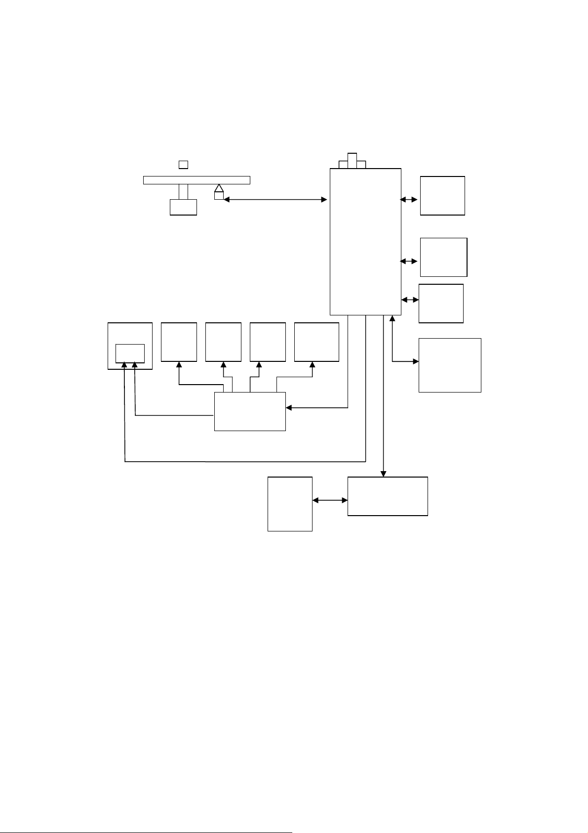
4. Block Diagram
Disc
Disc motor unit
Spindle
Motor
MT1389
(Decode/Servo)
ATAPI
Buffer Manager
Laser
pickup
Focus
Coil
Track
Coil
BA5954FP
4ch motor Drive
Sied
Motor
Loading
Motor
Demodulator
Error Correction
PLI
Focus & Tracking
Loading
SDROM
AuDdio
AMP
Video D/A
Filter
1/F
Conn
(front pannel)
Fiash
Memory
8Mbit
24CO2
System Controller
- 6 -
Page 8

2-1-2 DVD Processor Chip MTK1389F
Features
Super Integration DVD player single chip
z High performance analog RF amplifier
z Servo controller and data channel processing
z Disc compatibility: DVD, DVD-R, DVD-RW, DVD+R, DVD+RW, Audio CD, CD-R, CD-RW, VCD, SVCD,
MP3-CD, MP3-DVD, PCM, JPEG-CD, JPEG-DVD
z Format compatibility:MPEG-1, MPEG-2, MPEG-4,
MP3, WMA, PCM, and JPEG & AVI
Dolby Digital, DTS
z Unified memory architecture
z Versatile video scaling & quality enhancement
z OSD & Sub-picture
z 2-D graphic engine
z Global motion compensation (GMC)
z Quarter pixel accurate motion Compensation (Q-PEL)
z B-frame
z Higher bit-rate up to 10 Mbps
z Full function remote control
z Plays regional code encrypted (RCE) DVDs
z Selectable 4:3 Pan & Scan or 16:9 Widescreen format
z PAL & NTSC playback
z Multi-speed FF/ RW, slow motion & multi level zoom
High Performance Analog RF Amplifier
z Programmable fc
z Dual automatic laser power control
z Defect and blank detection
z RF level signal generato
- Audio
z Dolby Digital (AC -3)/EX decoding
z DTS/DTS -ES decoding
z MLP decoding for DVD-Audio
z MPEG-1 layer 1/layer 2 audio decoding
z MPEG-2 layer1/layer2 2-channel audio
z High Definition Compatible Digital (HDCD)
z Windows Media Audio (WMA)
z Advanced Audio Coding (AAC)
z Dolby ProLogic II
z Concurrent multi-channel and downmix out
z IEC 60958/61937 output
-TV Encoder
z Six 108MHz/12bit DACs
z Support NTSC, PAL-BDGHINM, PAL-60
z Support 525p, 625p progressive TV format
z Automatically turn off unconnected channels
z Support PC monitor (VGA)
z Support Macrovision 7.1 L1, Macrovision 525P
z and 625P
DivX 3.11, DivX 4.x, DivX5.x (Need licence), Xvid,
- 7 -
Page 9
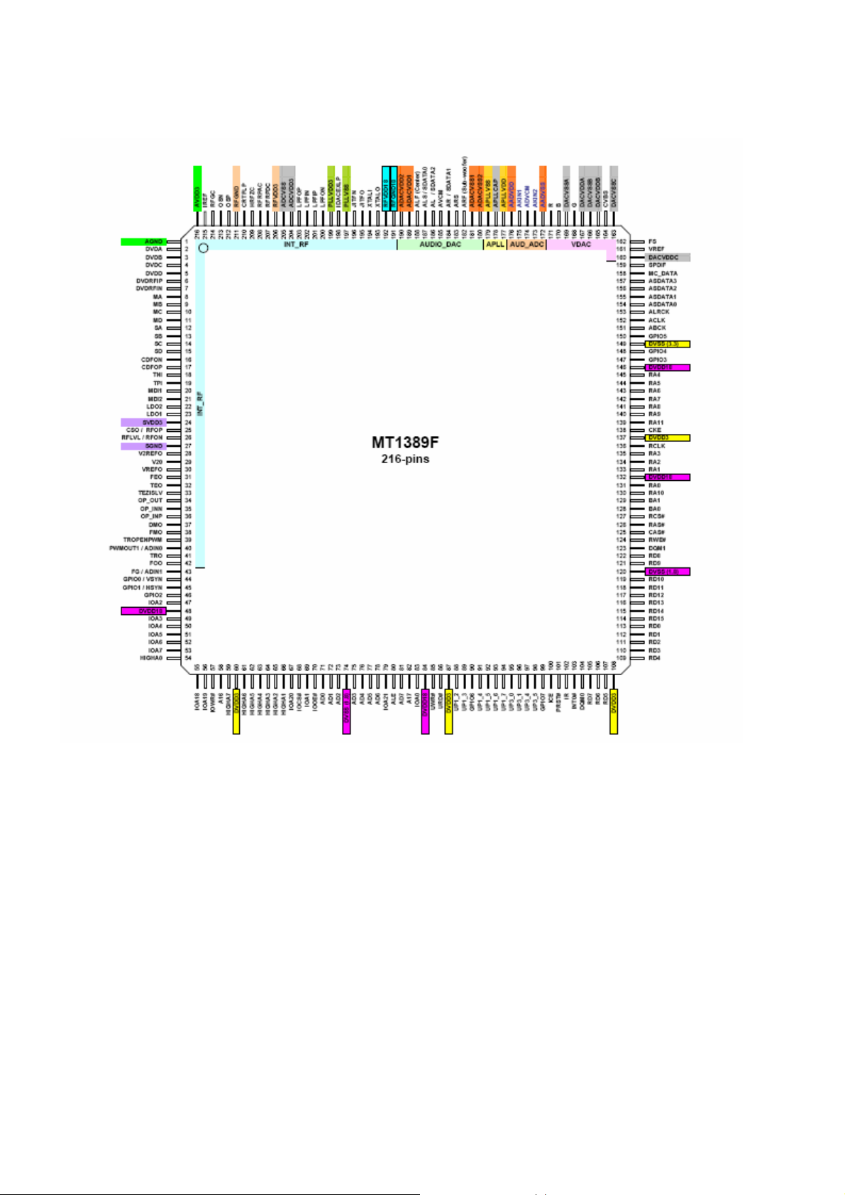
* Pinout Diagram
- 8 -
Page 10

PIN DESCRIPTON
- 9 -
Page 11
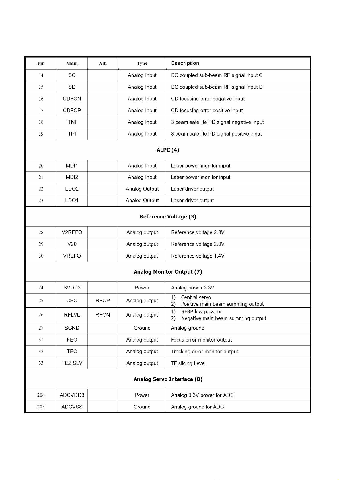
- 10 -
Page 12

- 11 -
Page 13

- 12 -
Page 14

- 13 -
Page 15

- 14 -
Page 16

- 15 -
Page 17

- 16 -
Page 18

- 17 -
Page 19

- 18 -
Page 20

- 19 -
Page 21

- 20 -
Page 22

- 21 -
Page 23

2-1-3 Serial EEPROM, 2K (256 x 8) (24C02) or 16 K (2048 x 8) (24C16)
24C02 is used for DVD player while 24C16 is for DVD receiver. The capacity is the only difference between
two kinds of serial EEPROM. Both of them use same package and have same pin configuration.
* Features
z Low-Voltage and Standard-Voltage Operation
-5.0 (V CC = 4.5V to 5.5V)
-2.7 (V CC = 2.7V to 5.5V)
-2.5 (V CC = 2.5V to 5.5V)
-1.8 (V CC = 1.8V to 5.5V)
z Internally Organized 128 x 8 (1K), 256 x 8 (2K), 512 x 8 (4K), 1024 x 8 (8K) or 2048 x 8 (16K)
z 2-Wire Serial Interface
z Schmitt Trigger, Filtered Inputs for Noise Suppression
z Bi-directional Data Transfer Protocol
z 100 kHz (1.8v, 2.5V, 2.7V) and 400 kHz (5V) Compatibility
z Write Protect Pin for Hardware Data Protection
z 8-Byte Page (1K, 2K), 16-Byte Page (4K, 8K, 16K) Write Modes
z Partial Page Writes Are Allowed
z Self-Timed Write Cycle (10 ms max)
z High Reliability
- Endurance: 1 Million Write Cycles
- Data Retention: 100 Years
-
- ESD Protection: >3000V
z Automotive Grade and Extended Temperature Devices Available
z 8-Pin and 14-Pin JEDEC SOIC, 8-Pin PDIP, 8-Pin MSOP, and 8-Pin TSSOP Packages
* Pin Configurations
* Pin Description
Pin Name Function
A0-A2 Address Inputs
SDA Serial Data
SCL Serial Clock input
WP Write Protect
NC No Connect
2-1-4: FLASH MEMORY( CMOS 16M (2M 8/1M 16) BIT)
GENERAL DESCRIPTION
The MBM29LV160TE/BE is a 16M-bit, 3.0 V-only Flash memory organized as 2M bytes of 8 bits each or 1M words
of 16 bits each. The MBM29LV160TE/BE is offered in a 48-pin TSOP (I), 48-pin CSOP and 48-ball FBGA
packages. The device is designed to be programmed in-system with the standard system 3.0 V VCC supply. 12.0
PP and 5.0 V VCC are not required for write or erase operations. The device can also be reprogrammed in
V V
standard EPROM programmers.
The standard MBM29LV160TE/BE offers access times of 70 ns and 90 ns allowing operation of high-speed
microprocessors without wait states. To eliminate bus contention the device has separate chip enable (CE), write
enable (WE), and output enable (OE) controls.
The MBM29LV160TE/BE is pin and command set compatible with JEDEC standard E
written to the command register using standard microprocessor write timings. Register contents serve as input
- 22 -
2PROMs. Commands are
Page 24

to an internal state-machine which controls the erase and programming circuitry. Write cycles also internally latch
addresses and data needed for the programming and erase operations. Reading data out of the device is similar
to reading from 5.0 V and 12.0 V Flash or EPROM devices.
The MBM29LV160TE/BE is programmed by executing the program command sequence. This will invoke the
Embedded Program
TM* Algorithm which is an internal algorithm that automatically times the program pulse widths
and verifies proper cell margins. Typically, each sector can be programmed and verified in about 0.5 seconds.
Erase is accomplished by executing the erase command sequence. This will invoke the Embedded Erase
TM*
Algorithm which is an internal algorithm that automatically preprograms the array if it is not already programmed
before executing the erase operation. During erase, the device automatically times the erase pulse widths and
verifies proper cell margins. (Continued)
(Continued)
Any individual sector is typically erased and verified in 1.0 second (if already preprogrammed).
The device also features sector erase architecture. The sector mode allows each sector to be erased and
reprogrammed without affecting other sectors. The MBM29LV160TE/BE is erased when shipped from the factory.
The device features single 3.0 V power supply operation for both read and write functions. Internally generated
and regulated voltages are provided for the program and erase operations. A low V
inhibits write operations on the loss of power. The end of program or erase is detected by Data Polling of DQ
by the Toggle Bit feature on DQ
6, or the RY/BY output pin. Once the end of a program or erase cycle has been
CC detector automatically
7,
completed, the device internally resets to the read mode.
The MBM29LV160TE/BE also has a hardware RESET pin. When this pin is driven low, execution of any
Embedded
Program Algorithm or Embedded Erase Algorithm is terminated. The internal state machine is then
reset to the read mode. The RESET pin may be tied to the system reset circuitry. Therefore, if a system reset
occurs during the Embedded Program Algorithm or Embedded Erase Algorithm, the device is automatically
reset to the read mode and will have erroneous data stored in the address locations being programmed or
erased. These locations need re-writing after the Reset. Resetting the device enables the system’s microprocessor
to read the boot-up firmware from the Flash memory.
Fujitsu’s Flash technology combines years of Flash memory manufacturing experience to produce the highest
levels of quality, reliability, and cost effectiveness. The MBM29LV160TE/BE memory electrically erases all bits
within a sector simultaneously via Fowler-Nordhiem tunneling. The bytes/words are programmed one byte/word
at a time using the EPROM programming mechanism of hot electron injection.
Embedded EraseTM and Embedded ProgramTM are trademarks of Advanced Micro Devices, Inc.
*:
- 23 -
Page 25

- 24 -
Page 26

2-1-5 512K X 16 Bit X 2 Banks Synchronous DRAM (A43L0616)
Features
JEDEC standard 3.3V power supply
LVTTL compatible with multiplexed address
Dual banks / Pulse RAS
MRS cycle with address key programs
- CAS Latency (2,3)
- Burst Length (1,2,4,8 & full page)
- Burst Type (Sequential & interleave)
All inputs are sampled at the positive going edge of the system clock
Burst Read Single-bit Write operation
DQM for masking
Auto & self refresh
64ms refresh period (4K cycle)
50 Pin TSOP (II)
- 25 -
Page 27

Pin Configuration
- 26 -
Page 28

Block Diagram
Pin Descriptions
Symbol Name Description
CLk System Clock Active on the positive going edge to sample all inputs
CS Chip Select Disables or Enables device operation by masking or enabling
all inputs except CLK, CKE and L(U)DQM
Masks system clock to freeze operation from the next clock cycle.
CKE Clock Enable
CKE should be enabled at least one clock + tss prior to new
command.
Disable input buffers for power down in standby.
A0~A10/AP Address
Row/Column addresses are multiplexed on the same pins.
Row address: RA0 ~ RA10, Column address: CA0 ~ CA7
BA Bank Select Address
Selects bank to be activated during row address latch time.
Selects band for read/write during column address latch time.
RAS Row address Strobe
Latches row addresses on the positive going edge of the CLK with
RAS low.
Enables row access & precharge.
CAS
Column Address Strobe
Latches column addresses on the positive going edge of the CLK
with CAS low. Enables column access.
WE Write Enable Enables write operation and Row precharge.
L(U)DQM
Data Input/Output Mask
Makes data output Hi-Z, t SHZ after the clock and masks the output.
Blocks data input when L(U)DQM active.
DW0-15 Data Input/Output Data inputs/outputs are multiplexed on the same pins.
VDD/VSS Power Supply/Ground Power Supply: +3.3V±0.3V/Ground
VDDQ/VSSQ
Data Output
Provide isolated Power/Ground to DQs for improved noise immunity.
Power/Ground
NC/RFU No Connection
- 27 -
Page 29

3. Product Specifications
Playback System
DVD Video
Video CD (1.1, 2.0, 3.0)
SVCD and CVD
CDDA
CD-ROM with MP3 data
PICTURE CD
Television Signal System
NTSC/PAL
Video Performance
Video Out 1 Vpp into 75 ohm
S-Video Out Y: 1Vpp into 75 ohm
C: 0.286 Vpp into 75 ohm
D/A Converter 27MHz/10bit
Audio Performance
Frequency
Response
Output Level Analog: 2Vrms(1KHZ)
D/A Converter 96KHz/24bit
S/N Ratio 90dB
Connections
Coaxial digital out X1
Audio Analog out for 2-channel X1
S-Video out X1
Power Supply
Power Source AC 230V, 50Hz
Power Consumption 15 Watt
Set
Dimensions (W X H X D) 360 X 45 X 270 (mm)
Net Weight 2.2 Kg
Gross Weight 3.0 Kg
DVD VIDEO (PCM 96KHz) 20Hz~44KHz(±1dB)
DVD VIDEO (PCM 48KHz) 20Hz~22KHz(±0.5dB)
CD: 20Hz~22KHz(±0.5dB)
Digital: 1.15 Vpp
- 28 -
Page 30

4. Upgrading System and Changing the Region
Code
MTK upgrade:
1. Name upgrade file as "MTK.BIN"(must be in big caps)
2. Record it in a CD-R/W (It can be enclosed a sub-directory which size is about 30M, and the file content can
be letter or non used file.)
disc Format: (advise to use the tool NERO burning ROM)
Disc volume: MEDIATEK, ISO9660 LEVEL1, MODE1,not JOILET.
3. Put the recorded disc into the DVD player, on the TV will show "upgrade?" after loading. Press PLAY button,
the player will automatically upgrade.
4. Do not shut down the player during upgrade, it will restart automatically after upgrade.
5. Upgrade finish!
How to change the region code:
1. Power on the machine, and press OPEN button to push the tray out.
2. Press SETUP button to enter the SETUP menu, and go to the PREFERENCE item by pressing left
button, then press 5 buttons in turn: 4,9,5,4,0
3. A edit box will be displayed, you can change the region code to 1-6 with UP/DOWN button, the num 0
means REGION FREE. And then press SETUP button to exit (FOR 1379)
4. A item named VERSION will be displayed, get into the page, you can change the region code to 1-6
with UP/DOWN button, the num 0 means REGION FREE. And then press SETUP button to exit (for
1369)
- 29 -
Page 31

5. Operating Instruction
Please refer to the User’s Manual for the operating instruction
of the system.
Maintenance & Troubleshooting
How to handle discs Disc Compatibility
To handle, clean and protect discs
● Do not touch the playing side of a disc
● Do not stick any paper or glue strip on a
disc.
How to clean discs
● Finger prints and dust on surface can
affect the sound and picture quality.
Clean discs regularly with a soft cotton
cloth from disc center to outside.
● For sticky dust, wipe it with wet cloth and
with dry cloth, Any kind of solvent, such
as diluting agent, gasoline, liquid
detergent, gasoline liquid detergent anti
– static aerosol used for vinylon LP, may
cause disc damage.
How to protect discs
● Keep away from the direct sunshine or
any heat source.
● Do not put discs in damp or dirty places,
such as bathroom or near humidifiers.
Store discs vertically in disc box and
store in a dry place. Piling discs on to top
of each other or excess weight load on
disc box may cause the disc to warp.
● Some DVD discs may have special
requirements for playing, with which this player
may not be compatible. Please refer to
specifications on individual disc.
DISC
TYPE
DVD
CD-DA AUDIO 12CM About 74 minutes
MP3 AUDIO 12CM About 300 minutes
Content Size Total Play time
About 2hrs.
(Single side & single
layer)
About 4hrs.
(Single side & double
AUDIO/
VIDEO
12CM
layer)
About 4hrs.
(Double side & Single
layer)
About 8hrs.
(Double side & double
layer)
Discs types
This DVD player can play the following types of
discs: Discs other than listed above cannot be
player by this player.
This player uses NTSC/PAL color system. It cannot
play discs recorded with other systems, such as
SECAM.
Region code
The region code for this player is 5, which
indicates the applicable. The disc with code
number other than 5 cannot be player on this
player and screen will indicate the unconformity.
Copyright
According to the related law, DVD discs without
proper authorization are not allowed to be copied
broadcast cable broadcast, played publicly or
rented. As DVD discs are anti-piracy the copied
content is distorted.
TV system
Connect this player to a PAL/NTSC compatible TV.
- 30 -
Page 32

Problems and Solutions
If a fault occurs, first check the points listed below before taking the set for repair.
If you are unable to remedy a problem by following these hints, consult your
dealer or service centre.
WAR NING: Under no circumstances should you try to repair the set yourself, as this would invalidate the
guarantee.
Problems Cause Solution
No power
indication
No picture
No sound
Picture
distortion
Brightness
unstable or
noisy
The player
does not
work
No response
to key press
Remote
control does
not work
Battery power exhausted Replace with new batteries.
Power plug not connected
TV has not been set to the
correct video input
Video cable not firmly
connected.
Audio cable not connected
tightly
Power of audio apparatus is
off
Audio output setting is
incorrect
Disc is dirty
Fast forward/backward is
activated
Affected by anti-piracy circuit
No disc Load a disc.
Disc not compatible
Tdohe disc is placed upside
wn
The disc not put in the tray
correctly
Disc is dirty Clean the disc.
Player setting are incorrect Change the setting via the setup menu.
Parental lock is in effect Disable this function or reset the rating level.
Interference of power wave or
other factors such as static
interference
The remote control not
pointed at the remote sensor
on the front panel of the
player
The remote control is out of
specified range
Note:
This produce incorporates copyright protection technology that is protected by method claims of certain of
certain U.S. patent and other intellectual Property rights owned by Macrovision Corporation and other rights
owners. Use of this copyright protection technology must be authorized by Macrovision Corporation and is
intended for home and other limited viewing users only, unless otherwise authorized by Macrovision
Corporation. Reverse engineering or disassembly is prohibited.
Plug the power cord into the power supply
Set correct TV video input format for receiving
the player’s output signals.
Firmly insert the video cable ends to the
related terminals.
Firmly insert the audio cable ends to the
related terminals.
Turn on the power of audio apparatus.
Setup audio output correctly via the setup
menu.
Take out the disc and clean.
The picture may be distorted during fast
forward /backward playback.
Connect the player directly to TV.
Load a compatible disc (Check the disc format
and its colour system).
Load a compatible disc (Check the disc format
and its colour system).
Check disc is put in correctly.
Turn off the main switch or pull out the power
plug, plug it in and turn on the power again.
Point the remote control at the remote sensor.
Make sure the remote control range within 7
meters to the remote sensor.
- 31 -
Page 33

6.Disassembly and Reassembly
- 32 -
Page 34

A
7.Troubleshooting
No power Insert the AC power plug securely into the power outlet.
Make sure that the equipment is connected properly.
No picture
No sound Make sure that the equipment is connected properly.
Distorted sound
No fast forward or fast reverse
No proper aspect ratio
No operations can be performed
with the remote controller
No button operation
udio soundtrack and/or Subtitle
language is not the one you
selected.
No Angle change
Make sure that the input setting for TV is Video (AV).
Make sure that the input settings for the TV and stereo system are
correct.
Some discs may have sections that prohibit fast forward or fast
reverse.
Select the correct setup for TV aspect ratio that matches your TV
set.
Check the batteries are installed with the correct polarities.
Point the remote control unit at the remote control sensor and
operate.
Remove the obstacles between the remote control unit and remote
control sensor.
Set the POWER button to OFF and then back to ON.
Alternatively, turn off the power, disconnect the power plug and
then reconnect it.
If the audio soundtrack and /or subtitle language does not exist on
the disc, the language selected at the initial settings will not be
seen.
This function is dependent on software availability. Even if a disc
has a number of angles recorded, these angles may be recorded
for specific scenes only.
- 33 -
Page 35

8. Block Diagram
- 34 -
Page 36

9. Circuit Diagrams
R42
10K
AVCC
0.1U
C39
RFVDD3
R118
100U/16V
6.8
E11
C114
0.1U
PLLVDD3
V1P4
[1,2]
[1]
JITFN
[1]
JITFO
[1]
X1
[1]
XO
APLLVDD3
AADVDD3
DV33
V18
[1,2]
100K
D-3
G-1
S-2
2SK3018
SPP11N60C3
Q9
J5
SANYO_DU34
HD60-24SMD
FOC-
FOC+
RAD+
RAD-
LDSW
RFO
GND4
V20
VCC2
GND3
DVD_VR
CD_VR
CD_LD
MDI
VCC1
GND2
DVD_LD
GND1
DMSO
[2]
FMSO
[2]
TRSO
[2]
[2]
FOSO
V1P4
R51
C
D
A
B
F
E
24
23
22
21
20
19
18
17
16
15
14
13
12
11
10
9
8
7
6
5
4
3
2
1
G
(1)
(2)
(3)
(4)
(5)
(6)
(7)
(8)
(9)
(10)
(11)
(13)
(14)
(15)
(17)
(18)
(19)
(20)
(21)
(23)
Q7
3904
S
D
R38
0
FF+
T+
TC
D
IOA
RFO
A
B
F
V20
AVCC1
E
DVD_VR
CD_VR
LD_CD
MD11
AVCC1
LD_DVD
CD_VR
100U/10V
C5
0.015U
R35
S
D
SPP11N60C3
2SK3018
Q8
R36
0
DVD_VR
E15
G
C81
0.1U
10K
R37
100K
C106
0.1U
V20
C83
330P
[1]
600/0603
C3
330P
R11
1
AVCC
[1,2]
FF+
T+
T-
R12
150K
L2
10uH
[2]
[2]
[2]
[2]
FB11
V1P4
IOA
10uH
L1
R27
R95
R97
R29
OP+
[1]
Q6
8550
Q5
8550
47U/10V
[3]
[3]
[2]
R13
R32
B-1
E6
10K
15K
[2]
18K
20K
VSYNC#
HSYNC#
C8
C-3
E-2
TROPEN
STBY
V18
2200P
680K
R34
R33
680K
LDO2
LDO1
C13
C15
C105
C10
0.1U
OPO
4.7
4.7
C16
1U
C17
1U
C14
C109
RFVDD3
0.1U
[1]
[1]
E9
47U/16V
RFV33
E8
47U/16V
1U
1U
1U
NC
V2P8
C9
0.1U
R31
A2
A3
A4
A5
A6
A7
A8
V20
OP-
OP+
RFVDD3
100K
R45
C99
15K
R49
0.1U
RFVDD3
C25
0.1U
1
AGND
2
DVDA
3
DVDB
4
DVDC
5
DVDD
6
DVDRFIP
7
DVDRFIN
8
MA
9
MB
10
MC
11
MD
12
SA
13
SB
14
SC
15
SD
16
CDFON
17
CDFOP
18
TNI
19
TPI
20
MDI1
21
MDI2
22
LDO2
23
LDO1
24
SVDD3
25
CSO/RFOP
26
RFLVL/RFON
27
SGND
28
V2REFO
29
V20
30
VREFO
31
FEO
32
TEO
33
TEZISLV
34
OP_OUT
35
OP_INN
36
OP_INP
37
DMO
FMO
TRO
FOO
0
ADIN
DMO
38
FMO
39
TROPENPWM
40
PWMOUT1/ADIN0
41
TRO
42
FOO
43
FG/ADIN1
44
GPIO0/VSYNC#
45
GPIO1/HSYNC#
46
GPIO2
47
IOA2
48
DVDD18
49
IOA3
50
IOA4
51
IOA5
52
IOA6
53
IOA7
54
HIGHA0
C98
0.1U
212
213
214
215
216
OSP
OSN
IREF
RFGC
AVDD3
IOA1856I0A1957IOWR#58A1659HIGHA760DVDD361HIGHA662HIGHA563HIGHA464HIGHA365HIGHA266HIGHA167IOA2068IOCS#69IOA170I00E#71AD072AD173AD274DVSS75AD376AD477AD578AD679IOA2180ALE81AD782A1783IOA084DVDD18
55
C34
0.1U
0.033U
C91
210
211
RFGND
CRTPLP
1000P
C26
208
209
HRFZC
RFRPAC
20P
0.1U
C24
C33
RFVDD3
205
206
207
RFRPDC
RFVDD3
0.047U
C29
202
203
204
LPFOP
ADCVSS
ADCVDD3
LPFIN
0.047U
C28
200
201
LPFIP
10U/10V
0.47U/NC
E17
C36
PLLVDD3
197
198
199
LPFON
PLLVDD3
IDACEXLP
195
196
JITFN
JITFO
PLLVSS
MT1389E
193
194
XTALI
U4
RFV18
191
192
XTALO
RFVDD18
RFGND18
ADACVDD3
187
188
189
190
ALF(CTR)
ADACVDD1
ADACVDD2
ALS/SDATA0
C32
0.1U
175
176
177
AKIN1
AADVDD
APLLVDD
10U/10V
E16
ADVCM
172
173
174
AKIN2
ADVCM
171
AADVSS
100
180
181
182
ARF(SW)
ADACVSS1
ADACVSS2
C90
1500P
178
179
APLLVSS
APLLCAP
10U/10V
E28
183
184
185
186
ARS
AVCM
AL/SDATA2
AR/SDATA1
UWR#86URD#87DVDD388UP1_289UP1_390GPIO691UP1_492UP1_593UP1_694UP1_795UP3_096UP3_197UP3_498UP3_599GPIO7
85
165
166
167
168
169
170
B/CB/SC
DACVSSB
DACVSSA
DACVDDA
G/Y/SY/CVBS
R/CR/CVBS/SY
ICE
PRST#
INTO#
DQMO#
RD7
101
102IR103
104
105
106
163
164
CVBS
DACVSSC
DACVDDB
VREF
DACVDDC
SPDIF
MC_DATA
ASDATA3
ASDATA2
ASDATA1
ASDATA0
ALRCK
ACLK
ABCK
GPIO5
DVSS
GPIO4
GPIO3
DVDD18
RA4
RA5
RA6
RA7
RA8
RA9
RA11
CKE
DVDD3
RCLK
RA3
RA2
RA1
DVDD18
RA0
RA10
BA1
BA0
RCS#
RAS#
CAS#
RWE#
DQM1
RD8
RD9
DVSS
RD10
RD11
RD12
RD13
RD14
RD15
RD0
RD1
RD2
RD3
RD4
RD6
RD5
DVDD3
107
108
FS
162
161
160
159
158
157
156
155
154
153
152
151
150
149
148
147
146
145
144
143
142
141
140
139
138
137
136
135
134
133
132
131
130
129
128
127
126
125
124
123
122
121
120
119
118
117
116
115
114
113
112
111
110
109
FS
VREF
MA4
MA5
MA6
MA7
MA8
MA9
MA11
MA3
MA2
MA1
MA0
MA10
DQ8
DQ9
DQ10
DQ11
DQ12
DQ13
DQ14
DQ15
DQ0
DQ1
DQ2
DQ3
DQ4
DACVDD3
ASPDIF
RGB-SWITCH
FS1
FSO
ASDATA0
MA[0:11]
DQ[0:15]
[3]
[3]
[3]
[2]
[2]
[3]
[1]
[2]
0.1U
TROUT
TRIN
LIMIT
BA1
BA0
CS#
RAS#
CAS#
WE#
DQM1
C22
[2]
[2]
[1]
DCKE
DCLK
[3]
[3]
[3]
[3]
[3]
[3]
[3]
[3]
[3]
R19
560
ACENTER
ALS
AL
AR
ARS
ASUBW
[1]
AKIN-1-2
R
VB
G
CVBS
JITFO
[2]
[2]
[2]
[2]
[2]
[2]
[1]
[1]
[3]
[3]
[3]
[3]
[2]
XO
X1
Y2
27MHz
R39
390P
C30
2.7uH
100K
R46
750K
L3
C37
1000P
C38
33P
C42
33P
JITFN
[1]
C92
0.1U
V20
47U/10V
TO_AV/6P_2.0
E7
C12
0.1U
C6
2200P
URST#
[1]
A[0:21]
AD[0:7]
C110
0.1U
C97
0.1U
J3
[3]
[1]
[3]
[3]
[2]
DV33
DOWNLOAD/4P_2.0
1
2
RXD
3
TXD
4
TRCLOSE
IOA
[1]
DQ7
DQ6
DQ5
DQM0
URST#
SDA
SCL
A1
A9
A18
A19
A16
A14
A15
[3]
[3]
VCC
IR
VSTB
VSCK
VSDA
100U/16V
J4
1
2
3
4
5
6
7
PWR#
[3]
E31
A13
C74
0.1U
A20
A10
A12
A11
VCC
R21
10K
C77NCC84NCC101
PCE#
[3]
AD0
PRD#
[3]
AD1
VCC
AD2
NC
AD3
R3
10K
AD4
AD5
AD6
R5
10K
ASDATA0
A21
AD7
R10
10K
A17
A0
[1]
R25
10
C4
100P
C111
0.1U
C113
0.1U
C27
0.1U
C107
0.1U
C88
0.1U
C93
0.1U
C89
0.1U
C95
0.1U
C96
0.1U
DV33
D1
OP-
R104
10K
E5
100U/16V
SP-
[2]
DV33
R4
10K
SPI-
6
5
4
3
2
1
J1
V2P8
E10
47U/10V
SP+
LIMIT
SLSL+
C11
0.1U
[2]
[2]
[2]
[1]
150K
R30
1N4148
Page 37

VCC
R82
4.7K
D15
1N4148
Q16
3906
D14
1N4148
E38
100U/16V
+12V
R81
22K
R80
470
E34
100U/16V
Q13
3906
AUDIO_MUTE
-12V
R77
100K
R23
100
A_MUTE
J6
[2]
Q14
FB26
FB25
LCH
RCH
[3]
[3]
R7
0 OR NC
AL
[1]
+12V
-12V
1
2
3
4
D10
AKIN-1-2
VCC
R52
[1]
75
[1]
AR
E30
10U/16V
R8
10K
E29
10U/16V
R63
10K
R65
10K
C48
1000P
C49
1000P
R68
30K
R71
5.1K
R70
30K
R76
5.1K
C51
2
3
C52
6
5
100P
A_MUTE
A_MUTE
R86
560
R84
560
Q15
3904
3904
E36
-
+
U9-A
-
+
1
100P
7
U9-B
10U/16V
[2]
E35
10U/16V
[2]
[1]
FSO
+12V
R43
R44
2.2K
1K
R28
1K
Q1
3904
SCART
R48
2.2K
R47
75
Q2
3904
[3]
ASPECT
[2]
DV33
REGO1
TRB1
[2]
Q22
SS8550
R58
R59
10K
10K
D11
R62
R64
10K
10K
Q23
SS8550
V18
TRB2
REGO2
[2]
[2]
[1]
[1]
ASUBW
[1]
ALS
ACENTER
R14
0 OR NC
E44
10U/16V
R15
0 OR NC
E41
10U/16V
R16
0 OR NC
E46
10U/16V
R41
10K
R128
10K
R67
10K
C69
1000P
C65
1000P
C124
1000P
R69
30K
R78
5.1K
R55
30K
R56
5.1K
R129
30K
R130
5.1K
C123
2
3
C68
2
3
C128
6
5
-
+
-
+
-
+
100P
U10-A
100P
U11-B
100P
U11-A
1
7
1
[2]
[2]
[2]
E43
10U/16V
A_MUTE
E40
10U/16V
A_MUTE
E45
10u/16v
A_MUTE
R66
560
R108
560
3904
3904
R40
560
3904
Q19
Q12
Q10
FB31
FB29
FB32
SUB
LSCH
CENT
[3]
[3]
[3]
[2,3]
[1]
MO_VCC
RGB-SWITCH
VCC
[1]
[2]
[1]
[1]
[1]
[1]
[1]
[1]
[1]
R20
4.7K
R18
SL+
FMSO
TRB2
TRSO
V1P4
STBY
R26
T+
SL-
[1]
FS1
FB30
RSCH
[3]
R94
10K
R57
30K
R22
5.1K
DV33
R93
10K
C23
0.1U
R17
68
2.2K
T-
10K
R50
Q3
3906
C75
0.1U
15
16
17
18
19
20
21
22
23
24
25
26
27
28
VOTK+
VOTKVOLD+
VOLDVCC2
NC
VCTL
GND
VINLD
NC
TRB2
VINTK
BIAS
MUTE
R24
4.7K
U6
C63
0.1U
VOFC+
VOFCVOSL-
VOSL+
VOTR+
VOTR-
VCC
REV
FWD
REGO1
VINSL+
REGO2
TRB1
VINFC
[3]
RGB-SW
14
13
12
11
10
9
8
7
6
5
4
3
2
1
F+
[1]
F-
[1]
SP-
[1]
SP+
[1]
LOAD+
[2]
LOAD-
[2]
TROPEN
TRCLOSE
REGO1
DMSO
REGO2
TRB1
FOSO
[2]
[2]
[1]
[1]
[1]
[2]
[1]
MO_VCC
C2
0.1U
E1
100U/16V
[1]
ARS
0 OR NC
E26
10U/16V
[2]
[2]
R60
10K
[1]
[1]
C64
1000P
TRIN
TROUT
LOAD+
LOAD-
C47
6
5
-
+
100P
U10-B
7
[2]
TRAY/5P_2.0
1
2
3
4
5
E42
10U/16V
A_MUTE
J2
R61
560
Q11
3904
MOTOR DRIVER SECTION
Page 38

R1 WAITING TO DEBUG
16MFLASH R20
32MFLASH R20 R21
A1
A2
A3
A4
A5
A6
A7
A8
A9
A10
A11
A12
A13
A14
A15
A16
A17
A18
A19
A20
A21
[1]
[1]
[1]
PRD#
PCE#
PWR#
28
12
26
11
14
25
24
23
22
21
20
19
18
48
17
16
10
15
8
7
6
5
4
3
2
1
9
R2
R1
A0
A1
A2
A3
A4
A5
A6
A7
A8
A9
A10
A11
A12
A13
A14
A15
A16
A17
A18
A19
A20
G
RP
RB
E
W
(WP)
A[0:21]
U2
DQ0
DQ1
DQ2
DQ3
DQ4
DQ5
DQ6
DQ7
DQ8
DQ9
DQ10
DQ11
DQ12
DQ13
DQ14
DQ15A-1
BYTE
(VPP)
VSS0
VSS1
VCC
10K
10K
29
31
33
35
38
40
42
44
30
32
34
36
39
41
43
45
47
13
27
46
37
[1]
AD[0:7]
C35
0.1U
AD0
AD1
AD2
AD3
AD4
AD5
AD6
AD7
A0
C1
0.1U
[1]
FB17
600/0603
E4
100U/16V
DV33
DBA0
[1,3]
[1,3]
SDCLK
SDCKE
DCS#
DRAS#
DCAS#
DWE#
DQM0
DQM1
MA[0:11]
[1,3]
MA0
MA1
MA2
MA3
MA4
MA5
MA6
MA7
MA8
MA9
MA10
21
22
23
24
27
28
29
30
31
32
20
19
35
34
18
17
16
15
14
36
33
37
26
50
GND_D
KM416S1020BT
A0
A1
A2
A3
U5
A4
A5
A6
A7
A8
A9
A10
BS/A11
CLK
CKE
CS
RAS
CAS
WE
LDQM
UDQM
NC
NC/VREF
GND3
GND6
DQ0
DQ1
DQ2
DQ3
DQ4
DQ5
DQ6
DQ7
DQ8
DQ9
DQ10
DQ11
DQ12
DQ13
DQ14
DQ15
VCC1
VCC4
VCC2
VCC3
VCC5
VCC6
GND1
GND2
GND4
GND5
DQ[0:15]
2
DQ0
3
DQ1
5
DQ2
6
DQ3
8
DQ4
9
DQ5
11
DQ6
12
DQ7
39
DQ8
40
DQ9
42
DQ10
43
DQ11
45
DQ12
46
DQ13
48
DQ14
49
DQ15
1
25
7
13
38
44
4
10
41
47
SD33
GND_D
[1,3]
DV33
FB16
600/0603
100U/10V
E12
FB6
FB10
FB18
FB19
FB20
FB21
FB22
0.1U
C66
GND_D
600/0603
600/0603
600/0603
600/0603
600/0603
600/0603
600/0603
0.1U
C67
0.1U
C70
GND_D
0.1U
C71
0.1U
C72
SD33
0.1U
C73
[1]
[1]
[1]
[1]
0.1U
C7
[1]
[1]
[1]
[1]
BA0
BA1
DCLK
DCKE
CS#
RAS#
CAS#
WE#
RN2
RN1
[1,3]
[1,3]
MA0
MA1
MA2
MA3
MA4
MA5
MA6
MA7
MA8
MA9
MA10
MA11
MA[0:11]
33X4
33X4
[1,3]
DQM0
DQM1
DBA0
DBA1
SDCLK
SDCKE
DCS#
DRAS#
DCAS#
DWE#
23
24
25
26
29
30
31
32
33
34
22
35
20
21
38
37
19
18
17
16
15
39
64MB_SDRAM
A0
A1
A2
A3
A4
A5
A6
A7
A8
A9
A10
A11
BA0
BA1
CLK
CKE
CS
RAS
CAS
WE
DQML
DQMH
U3
DQ0
DQ1
DQ2
DQ3
DQ4
DQ5
DQ6
DQ7
DQ8
DQ9
DQ10
DQ11
DQ12
DQ13
DQ14
DQ15
VCC1
VCC2
VCC3
VCCQ1
VCCQ2
VCCQ3
VCCQ4
VSSQ1
VSSQ2
VSSQ3
VSSQ4
VSS1
VSS2
VSS3
2
4
5
7
8
10
11
13
42
44
45
47
48
50
51
53
1
14
27
3
9
43
49
6
12
46
52
28
41
54
DQ[0:15]
SD33
[1,3]
DQ7
DQ6
DQ5
DQ4
DQ3
DQ2
DQ1
DQ0
DQ8
DQ9
DQ10
DQ11
DQ12
DQ13
DQ14
DQ15
GND_D
DV33
DV33
FB12
FB8
0.1U
600/0603
220U/10V
E25
600/0603
C21
ADACVDD3
6800P
C44
DACVDD3
10U/10V
E13
RFVDD3
C20
2200P
DV33
C19
0.01U
FB1
1000U/10V
600/0603
C18
0.1U
600/0603
E20
RFV33
FB13
AADVDD3
6800P
C87
C43
0.1U
24C02
1
A0
2
A1
3
A2
4
GND5SDA
U1
VCC
WP
SCL
8
7
6
DV33
R61KR9
1K
SCL
SDA
[1]
[1]
[1]
[1]
CVBS
VCC
D4
BA99
CVBS0
[3]
VCC
[3]
[3]
[1]
B/U
R/V
ASPDIF
J10
1
2
3
4
5
R73
75
C55
220P
L6
L
C59
100P
VCC
L
L7
G
R74
75
[3]
G/Y
C56
220P
C60
100P
1
D7
1N4148
D6
1N4148
YUV
J8
G/Y
[3]
[2,3]
[2,3]
[3]
[2]
[2]
[3]
[3]
[3]
[1]
[1]
RCH
LCH
CVBS0
RGB-SW
ASPECT
R/V
G/Y
B/U
HSYNC#
VSYNC#
12
11
10
9
8
7
6
5
4
3
2
1
J12
2
[3]
R/V
3
DV33
FB15
600/0603
C40
0.1U
RFV33
E18
47U/16V
+5V
FB9
C41
0.1U
POWER CON
AVCC
600/0603
E24
47U/10V
E19
220U/10V
E22
47U/10V
V18
C94
0.1U
FB2
RFV18
600/0603
C31
0.1U
[3]
[3]
CVBS0
B/U
L
VB
[1]
DV33
FB14
600/0603
E21
47U/10V
MO_VCC
FB5
7
6
+5V
5
4
3
2
1
+P12
-P12
FB23
FB24
FB4
FB3
L
L
VCC
L
L
600/0603
C50
0.1U
C100
0.1U
+12V
E32
100U/16V
220U/10V
E14
-12V
C53
0.1U
APLLVDD3
C117
0.1U
E37
100U/16V
100U/10V
E23
G1
NEW_PART1
R
X2
X3
2
1
2
[1]
R75
75
R72
75
C57
220P
C54
220P
L5
L
J7
L8
C61
100P
C58
100P
4
5
6
[2,3]
[2,3]
J11
AUDIO2
[2,3]
LCH
RCH
LCH
1
2
3
4
5
VCC
VCC
D9
1N4148
D8
1N4148
D3
1N4148
SC
SY
R/V
B/U
[3]
[3]
[2,3]
[2]
[2]
[2]
[2]
RCH
LSCH
RSCH
CENT
SUB
10
11
12
13
14
6
7
8
9
D2
1N4148
VIDEO FILTER
Page 39

10. Wiring Diagram:
Output
to
Amplifier
Power
AV Output Board
Output
to
TV
Transformer
Power
Audio
stream
Video
stream
MPEG Board
Loader is
on the MPEG board
Front Panel
Control
Stream
- 38 -
 Loading...