


UTMC 5962P0153201TYX, 5962P0153201TYA, 5962P0153201QYX, 5962P0153201QYC, 5962P0153201QYA Datasheet
...Standard Products
QCOTSTM UT8Q1024K8 SRAM
Data Sheet
January, 2003
FEATURES
q25ns maximum (3.3 volt supply) address access time
qDual cavity package contains two (2) 512K x 8 industrystandard asynchronous SRAMs; the control architecture allows operation as an 8-bit data width
qTTL compatible inputs and output levels, three-state bidirectional data bus
qTypical radiation performance - Total dose: 50krad(Si)
INTRODUCTION
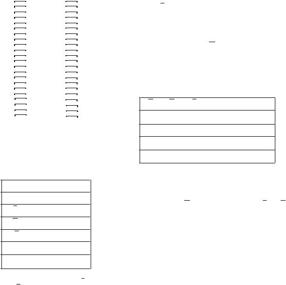
The QCOTSTM UT8Q1024K8 Quantified Commercial Off-the- Shelf product is a high-performance 1M byte (8Mbit) CMOS static RAM built with two individual 524,288 x 8 bit SRAMs with a common output enable. Memory access and control is provided by an active LOW chip enable (En), an active LOW output enable (G). This device has a power-down feature that reduces power consumption by more than 90% when deselected.
-SEL Immune >80 MeV-cm2/mg
-LETTH(0.25) = >10 MeV-cm2/mg
-Saturated Cross Section cm2 per bit, 5.0E-9
-<1E-8 errors/bit-day, Adams 90% geosynchronous heavy ion
qPackaging options:
-44-lead bottom brazed dual CFP (BBTFP) (4.6 grams)
qStandard Microcircuit Drawing 5962-01532
-QML T and Q compliant part
Writing to each memory is accomplished by taking one of the chip enable (En) inputs LOW and write enable (Wn) inputs LOW. Data on the I/O pins is then written into the location specified on the address pins (A0 through A18 ). Reading from the device is accomplished by taking one ofthe chip enable (En) and output enable (G) LOW while forcing write enable (Wn) HIGH. Under these conditions, the contents of the memory location specified by the address pins will appear on the I/O pins. Only one SRAM can be read or written at a time.
The input/output pins are placed in a high impedance state when the device is deselected (En HIGH), the outputs are disabled (G HIGH), or during a write operation (En LOW and Wn LOW).
W1 |
W0 |
E1 |
E0 |
A(18:0)
G
512K x 8 |
|
|
512K x 8 |
||
|
|
|
|
|
|
|
|
|
|
|
|
|
|
|
|
|
|
|
|
|
|
|
|
DQ(7:0)
Figure 1. UT8Q1024K8 SRAM Block Diagram
1
NC |
|
|
|
|
1 |
44 |
|
|
NC |
|
|
|
|||||||
NC |
|
|
|
|
2 |
43 |
|
|
E2 |
A0 |
|
|
|
|
3 |
42 |
|
|
NC |
|
|
|
|
A18 |
|||||
A1 |
4 |
41 |
|
|
|||||
A2 |
|
|
|
|
|
|
A17 |
||
|
|
|
|
5 |
40 |
|
|
||
A3 |
6 |
39 |
|
|
A16 |
||||
A4 |
|
|
|
|
|
|
A15 |
||
|
|
|
|
7 |
38 |
|
|
||
|
|
|
|
G |
|||||
E1 |
|
|
8 |
37 |
|
|
|||
DQ0 |
|
|
|
|
DQ7 |
||||
9 |
36 |
|
|
||||||
DQ1 |
|
|
DQ6 |
||||||
10 |
35 |
|
|
||||||
VDD |
|
|
|
|
|
|
VSS |
||
|
|
|
|
11 |
34 |
|
|
||
|
|
|
|||||||
VS S |
|
|
|
|
12 |
33 |
|
|
VDD |
|
|
|
|||||||
DQ2 |
|
|
|
|
13 |
32 |
|
|
DQ5 |
|
|
|
|||||||
DQ3 |
|
|
|
|
14 |
31 |
|
|
DQ4 |
|
|
|
|||||||
W1 |
|
|
|
|
15 |
30 |
|
|
A14 |
|
|
|
|||||||
A5 |
|
|
|
|
16 |
29 |
|
|
A13 |
|
|
|
|||||||
A6 |
|
|
|
|
17 |
28 |
|
|
A12 |
|
|
|
|||||||
A7 |
|
|
|
|
18 |
27 |
|
|
A11 |
|
|
|
|||||||
A8 |
|
|
19 |
26 |
|
|
A10 |
||
|
|
||||||||
|
|
|
|
|
|||||
A9 |
|
|
20 |
25 |
|
|
NC |
||
|
|
||||||||
W2 |
|
|
21 |
24 |
|
|
NC |
||
|
|
||||||||
|
|
|
|
|
|||||
NC |
|
|
22 |
23 |
|
|
NC |
||
|
|
||||||||
|
|
|
|
|
|
|
|
|
|
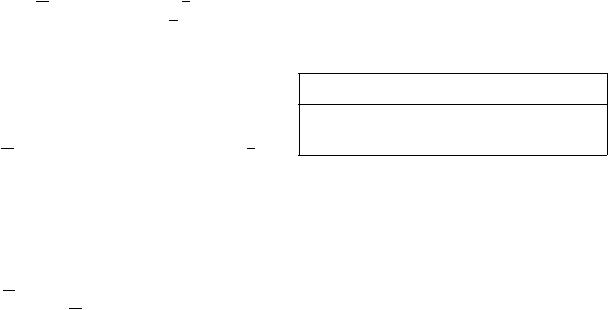
Figure 2. 25ns SRAM Pinout (44)
PIN NAMES
A(18:0) |
Address |
DQ(7:0) |
Data Input/Output |
En |
Device Enable |
Wn |
WriteEnable |
G |
Output Enable |
VDD |
Power |
VSS |
Ground |
Notes:
1.To avoid bus contention, on the DQ(7:0) bus, only one En can be driven low simultaneously while G is low.
DEVICE OPERATION
Each die in the UT8Q1024K8 has three control inputs called Enable (En), Write Enable (Wn), and Output Enable (G); 19 address inputs, A(18:0); and eight bidirectional data lines, DQ(7:0). The device enable (En) controls device selection, active, and standby modes. Asserting En enables the device, causes IDD to rise to its active value, and decodes the 19 address inputs to each memory die . Wn controls read and write operations. During a read cycle, G must be asserted to enable the outputs.
Table 1. Device Operation Truth Table
G |
Wn |
En |
I/O Mode |
Mode |
1 |
X |
1 |
3-state |
Standby |
X |
|
|
|
|
X |
0 |
0 |
Data in |
Write |
1 |
1 |
0 |
3-state |
2 |
|
|
|
|
Read |
0 |
1 |
0 |
Data out |
Read |
|
|
|
|
|
Notes:
1.“X” is defined as a “don’t care” condition.
2.Device active; outputs disabled.
READ CYCLE
A combination of Wn greater than VIH (min) with En and G less than VIL (max) defines a read cycle. Read access time is measured from the latter of device enable, output enable, or valid address to valid data output.
SRAM Read Cycle 1, the Address Access is initiated by a change in address inputs while the chip is enabled with G asserted and Wn deasserted. Valid data appears on data outputs DQ(7:0) after the specified tAVQV is satisfied. Outputs remain active throughout the entire cycle. As long as device enable and output enable are active, the address inputs may change at a rate equal to the minimum read cycle time (tAVAV).
SRAM Read Cycle 2, the Chip Enable-controlled Access is initiated by En going active while G remains asserted, Wn remains deasserted, and the addresses remain stable for the entire cycle. After the specified tETQV is satisfied, the eight-bit word addressed by A(18:0) is accessed and appears at the data outputs DQ(7:0).
SRAM Read Cycle 3, the Output Enable-controlled Access is initiated by G going active while En is asserted, Wn is deasserted, and the addresses are stable. Read access time is tGLQV unless tAVQV or tETQV have not been satisfied.
2
WRITE CYCLE
A combination of Wn less than VIL(max) and En less than
VIL(max) defines a write cycle. The state of G is a “don’t care” for a write cycle. The outputs are placed in the high-impedance state when eitherG is greater than V IH(min), or when Wn is less than VIL(max).
Write Cycle 1, the Write Enable-controlled Access is defined by a write terminated by Wn going high, with En still active. The write pulse width is defined by tWLWH when the write is initiated byWn, and by tETWH when the write is initiated byEn. Unless the outputs have been previously placed in the highimpedance state byG, the user must wait t WLQZ before applying data to the eight bidirectional pins DQ(7:0) to avoid bus contention.
Write Cycle 2, the Chip Enable-controlled Access is defined by a write terminated by the former of En or Wn going inactive. The write pulse width is defined by tWLEF when the write is initiated by Wn, and by tETEF when the write is initiated by the En going active. For the Wn initiated write, unless the outputs have been previously placed in the high-impedance state by G, the user must wait tWLQZ before applying data to the eight bidirectional pins DQ(7:0) to avoid bus contention.
TYPICAL RADIATION HARDNESS
The UT8Q1024K8 SRAM incorporates features which allow operation in a limited radiation environment.
Table 2. Typical Radiation Hardness
Design Specifications1
Total Dose |
50 |
krad(Si) nominal |
Heavy Ion |
<1E-8 |
Errors/Bit-Day |
Error Rate 2 |
|
|
|
|
|
Notes:
1.The SRAM will not latchup during radiation exposure under recommended operating conditions.
2.90% worst case particle environment, Geosynchronous orbit, 100 mils of Aluminum.
3
ABSOLUTE MAXIMUM RATINGS1
(Referenced to VSS)
SYMBOL |
PARAMETER |
VDD |
DC supply voltage |
VI/O |
Voltage on any pin |
TSTG |
Storage temperature |
PD |
Maximum power dissipation |
TJ |
Maximum junction temperature2 |
ΘJC |
Thermal resistance, junction-to-case3 |
II |
DC input current |
|
|
Notes:
LIMITS
-0.5 to 4.6V
-0.5 to 4.6V
-65 to +150°C
1.0W (per byte)
+150°C
10°C/W
±10 mA
1.Stresses outside the listed absolute maximum ratings may cause permanent damage to the device. This is a stress rating only, and functional operation of the device at these or any other conditions beyond limits indicated in the operational sections of this specification is not recommended. E xposure to absolute maximum rating conditions for extended periods may affect device reliability and performance.
2. Maximum junction temperature may be increased to +175 °C during burn-in and steady-static life. 3. Test per MIL-STD-883, Method 1012.
RECOMMENDED OPERATING CONDITIONS |
|
|
|||
|
SYMBOL |
|
PARAMETER |
|
LIMITS |
|
|
|
|||
|
VDD |
|
Positive supply voltage |
|
3.0 to 3.6V |
|
TC |
|
Case temperature range |
|
-40 to +125°C |
|
VIN |
|
DC input voltage |
|
0V to VDD |
4

DC ELECTRICAL CHARACTERISTICS (Pre/Post-Radiation)*
(-40°C to +125°C) (VDD = 3.3V + 0.3)
SYMBOL |
PARAMETER |
CONDITION |
MIN |
MAX |
UNIT |
||||
|
VIH |
High-level input voltage |
(CMOS) |
|
|
2.0 |
|
V |
|
|
VIL |
Low-level input voltage |
(CMOS) |
|
|
|
0.8 |
V |
|
|
VOL1 |
Low-level output voltage |
IOL = 8mA, VDD =3.0V |
|
|
|
0.4 |
V |
|
|
|
|
|
|
|||||
|
VOL2 |
Low-level output voltage |
IOL = 200mA,VDD =3.0V |
|
0.08 |
V |
|||
|
VOH1 |
High-level output voltage |
IOH = -4mA,VDD =3.0V |
|
|
2.4 |
|
V |
|
|
VOH2 |
High-level output voltage |
IOH = -200mA,VDD =3.0V |
VDD-0.10 |
|
V |
|||
|
|
1 |
Input capacitance |
¦ = 1MHz @ 0V |
|
|
|
20 |
pF |
|
CIN |
|
|
|
|
|
|
|
|
|
|
1 |
Bidirectional I/O capacitance |
¦ = 1MHz @ 0V |
|
|
|
24 |
pF |
|
CIO |
|
|
|
|
|
|
|
|
|
IIN |
Input leakage current |
VSS < VIN < VDD, VDD = VDD (max) |
-2 |
2 |
mA |
|||
|
IOZ |
Three-state output leakage current |
0V < VO < VDD |
|
|
-2 |
2 |
mA |
|
|
|
|
|
VDD = VDD (max) |
|
|
|
|
|
|
|
|
|
G = VDD (max) |
|
|
|
|
|
|
IOS |
Short-circuit output current |
0V < VO < VDD |
|
|
-90 |
90 |
mA |
|
|
|
2, 3 |
|
|
|
|
|
|
|
I |
DD |
(OP) |
Supply current operating |
Inputs: VIL = 0.8V, |
|
|
|
150 |
mA |
|
|
@ 1MHz |
VIH = 2.0V |
|
|
|
|
|
|
|
|
|
|
|
|
|
|
||
|
|
|
|
IOUT = 0mA |
|
|
|
|
|
|
|
|
|
VDD = VDD (max) |
|
|
|
|
|
IDD1 (OP) |
Supply current operating |
Inputs: VIL = 0.8V, |
|
|
|
220 |
mA |
||
|
|
|
@40MHz |
VIH = 2.0V |
|
|
|
|
|
|
|
|
|
IOUT = 0mA |
|
|
|
|
|
|
|
|
|
VDD = VDD (max) |
|
|
|
|
|
IDD2(SB) |
Nominal standby supply current |
Inputs: VIL = VSS |
|
-40°C and 25°C |
|
4 |
mA |
||
|
|
||||||||
|
|
|
@0MHz |
IOUT = 0mA |
|
|
|
|
mA |
|
|
|
|
En = VDD - 0.5, |
|
+125°C |
|
|
|
|
|
|
|
|
|
25 |
|
||
|
|
|
|
VDD = VDD (max) |
|
|
|
|
|
|
|
|
|
|
|
|
|
|
|
|
|
|
|
VIH = VDD - 0.5V |
|
|
|
|
|
|
|
|
|
|
|
|
|
|
|
Notes:
* Post-radiation performance guaranteed at 25°C per MIL-STD-883 Method 101 9 .
1.Measured only for initial qualification and after process or design changes that could affect input/output capacitance.
2.Supplied as a design limit but not guaranteed or tested.
3.Not more than one output may be shorted at a time for maximum duration of one second.
5
 Loading...