查询UC1524供应商
Advanced Regulating Pulse Width Modulators
UC1524
UC2524
UC3524
FEATURES
Complete PWM Power Control
•
Circuitry
Uncommitted Outputs for
•
Single-ended or Push-pull
Applications
Low Standby Current…8mA Typical
•
Interchangeable with SG1524,
•
SG2524 and SG3524, Respectively
DESCRIPTION
The UC1524, UC2524 and UC3524 incorporate on a single monolithic chip
all the functions required for the construction of regulating power supplies, in
verters or switching regulators. They can also be used as the control element
for high-power-output applications. The UC1524 family was designed for
switching regulators of either polarity, transformer-coupled dc-to-dc convert
ers, transformerless voltage doublers and polarity converter applications em
ploying fixed-frequency, pulse-width modulation techniques. The dual
alternating outputs allow either single-ended or push-pull applications. Each
device includes an on-chip reference, error amplifier, programmable oscilla
tor, pulse-steering flip-flop, two uncommitted output transistors, a high-gain
comparator, and current-limiting and shut-down circuitry. The UC1524 is
characterized for operation over the full military temperature range of -55°C
to +125°C. The UC2524 and UC3524 are designed for operation from -25°C
to +85°C and 0° to +70°C, respectively.
-
-
-
-
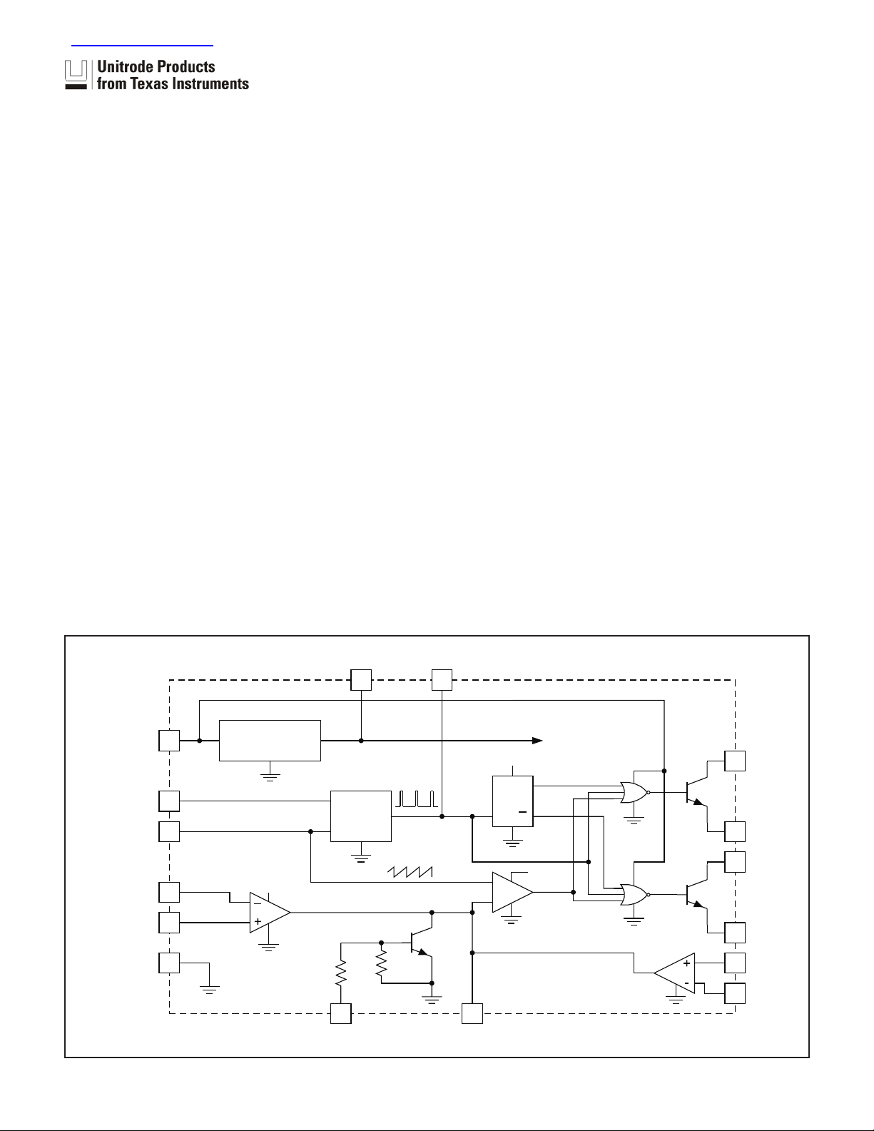
BLOCK DIAGRAM
15
V
IN
6
R
T
7
C
T
(RAMP)
INV INPUT
NI INPUT
GROUND
(SUBSTRATE)
1
2
8
REFERENCE
REGULATOR
+5V
EA
10
V
REF
16
OSC
1k
OSC OUT
COMPARATOR
10k
3
+5V TO ALL
INTERNAL
Q
QR
CIRCUITRY
+5V
CL
11
13
14
5
4
C
A
E
A
C
B
E
B
–SENSE
+SENSE
+5V 12
9
SHUTDOWN
COMPENSATION
SLUS180D - NOVEMBER 1999 - REVISED AUGUST 2002

ABSOLUTE MAXIMUM RATINGS (Note 1)
Supply Voltage, VCC(Notes 2 and 3) . . . . . . . . . . . . . . . . . 40V
Collector Output Current. . . . . . . . . . . . . . . . . . . . . . . . . 100mA
Reference Output Current . . . . . . . . . . . . . . . . . . . . . . . . 50mA
Current Through C
Power Dissipation at T
Power Dissipation at T
Terminal . . . . . . . . . . . . . . . . . . . . . . –5mA
T
= +25°C (Note 4). . . . . . . . . . 1000mW
A
= +25°C (Note 4). . . . . . . . . . 2000mW
C
Operating Junction Temperature Range . . . . –55°C to +150°C
Storage Temperature Range . . . . . . . . . . . . . –65°C to +150°C
Note 1: Over operating free-air temperature range unless oth
-
erwise noted.
Note 2: All voltage values are with respect to the ground termi
nal, pin 8.
Note 3: The reference regulator may be bypassed for operation
from a fixed 5V supply by connecting the V
CC
and ref
erence output pins both to the supply voltage. In this
configuration the maximum supply voltage is 6V.
Note 4: Consult packaging section of databook for thermal lim
itations and considerations of package.
RECOMMENDED OPERATING CONDITIONS
Supply Voltage, VCC. . . . . . . . . . . . . . . . . . . . . . . . . . 8V to 40V
Reference Output Current . . . . . . . . . . . . . . . . . . . . . 0 to 20mA
Current through C
Timing Resistor, R
Timing Capacitor, C
Operating Ambient Temperature Range
UC1524 . . . . . . . . . . . . . . . . . . . . . . . . . . . . –55°C to +125°C
UC2524 . . . . . . . . . . . . . . . . . . . . . . . . . . . . . –25°C to +85°C
UC3524 . . . . . . . . . . . . . . . . . . . . . . . . . . . . . . . 0°C to +70°C
Terminal . . . . . . . . . . . . . –0.03mA to –2mA
T
. . . . . . . . . . . . . . . . . . . . . 1.8kΩ to 100kΩ
T
. . . . . . . . . . . . . . . . . . . 0.001µF to 0.1µF
T
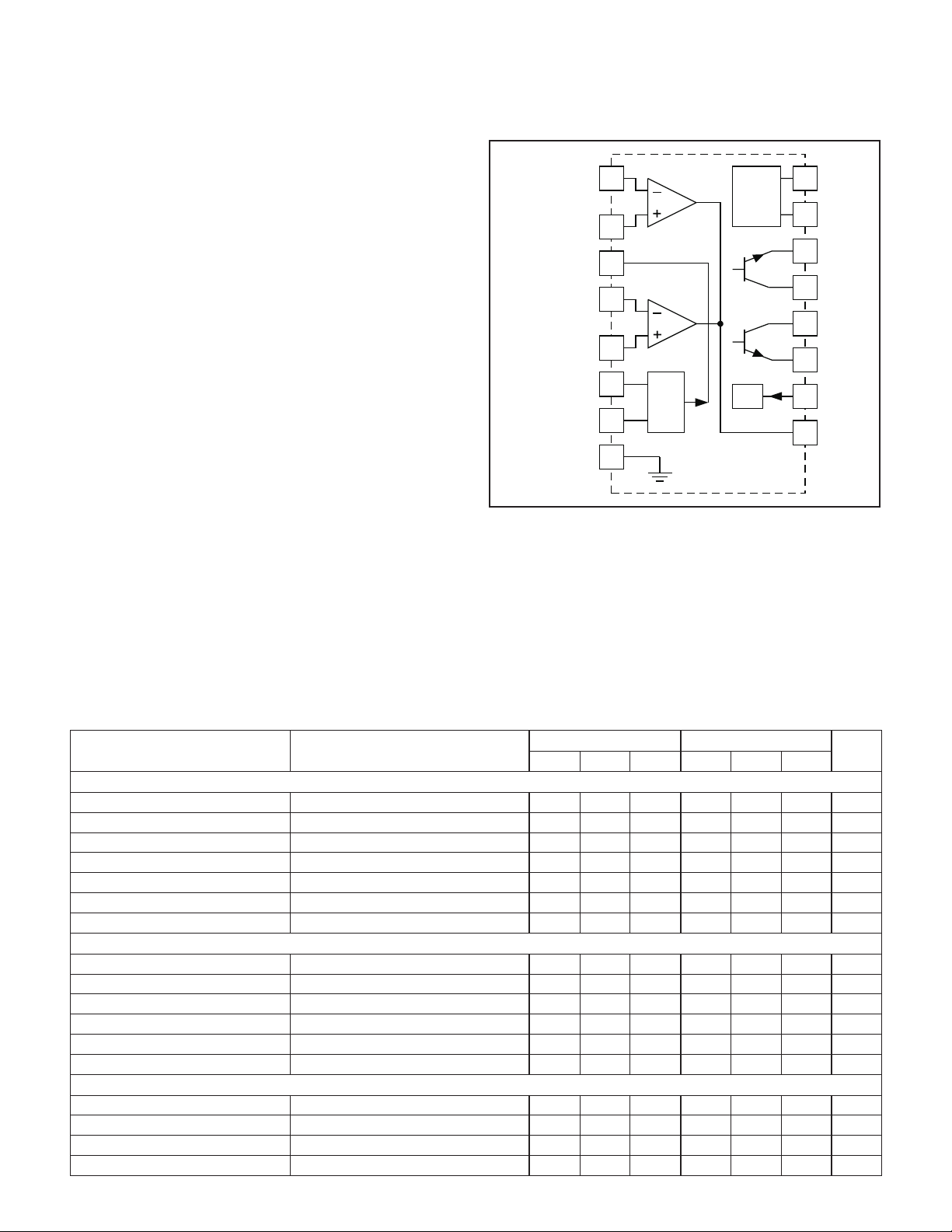
CONNECTION DIAGRAM
INV INPUT
NON INV
INPUT
OSC OUT
CLSENSE(+)
-
CLSENSE (–-)
-
-
R
C
GND
T
T
UC1524
UC2524
UC3524
1
EA
2
3
4
CL
5
6
OSC
7
8
REF
REG
S/D
16
15
14
13
12
11
10
V
REF
V
IN
E
B
C
B
C
A
E
A
S/D
9
COMP
ELECTRICAL CHARACTERISTICS: Unless otherwise stated, these specifications apply for T
for the UC1524, –25°C to +85°C for the UC2524, and 0°C to +70°C for the UC3524, V
T
A=TJ
.
= 20V, and f = 20kHz,
IN
= –55°C to +125°C
A
UC1524/UC2524 UC3524 UNITS
PARAMETER TEST CONDITIONS
MIN MAX MIN MAX
Reference Section
Output Voltage 4.8 5.0 5.2 4.6 5.0 5.4 V
Line Regulation V
Load Regulation I
Ripple Rejection f = 120Hz, T
Short Circuit Current Limit V
IN = 8 to 40V 10 20 10 30 mV
L = 0 to 20mA 20 50 20 50 mV
J = 25°C 66 66 dB
REF = 0, TJ = 25°C 100 100 mA
Temperature Stability Over Operating Temperature Range 0.3 1 0.3 1 %
Long Term Stability T
J = 125°C, t = 1000 Hrs. 20 20 mV
Oscillator Section
Maximum Frequency C
Initial Accuracy R
Voltage Stability V
= .001mfd, RT= 2kΩ 300 300 kHz
T
and CTConstant 5 5 %
T
= 8 to 40V, TJ= 25°C 1 1 %
IN
Temperature Stability Over Operating Temperature Range 5 5 %
Output Amplitude Pin 3, T
Output Pulse Width C
T
= 25°C 3.5 3.5 V
J
= .01mfd, TJ= 25°C 0.5 0.5
Error Amplifier Section
Input Offset Voltage V
Input Bias Current V
= 2.5V 0.5 5 2 10 mV
CM
= 2.5V 2 10 2 10
CM
Open Loop Voltage Gain 72 80 60 80 dB
Common Mode Voltage T
= 25°C 1.8 3.4 1.8 3.4 V
J
2
µs
µA

UC1524
UC2524
UC3524
ELECTRICAL CHARACTERISTICS: Unless otherwise stated, these specifications apply for T
for the UC1524, –25°C to +85°C for the UC2524, and 0°C to +70°C for the UC3524, V
T
.
A=TJ
PARAMETER TEST CONDITIONS
Error Amplifier Section (cont.)
Common Mode Rejection Ratio T
Small Signal Bandwidth A
Output Voltage T
Comparator Section
Duty-Cycle % Each Output On 0 45 0 45 %
Input Threshold Zero Duty-Cycle 1 1 V
Input Bias Current 1 1
Current Limiting Section
Sense Voltage Pin 9 = 2V with Error Amplifier
Sense Voltage T.C. 0.2 0.2 mV/°C
Common Mode Voltage T
Output Section (Each Output)
Collector-Emitter Voltage 40 40 V
Collector Leakage Current V
Saturation Voltage I
Emitter Output Voltage V
Rise Time R
Fall Time R
Total Standby Current (Note)
= 25°C 70 70 dB
J
V = 0dB, T
= 25°C 0.5 3.8 0.5 3.8 V
J
Maximum Duty-Cycle 3.5 3.5 V
Set for Maximum Out, T
= –55°C to 85°C
J
for the –1V to 1V Limit
= 125°C –0.3 +1 V
T
J
= 40V 0.1 50 0.1 50
CE
C = 50mA 1 2 1 2 V
= 20V 17 18 17 18 V
IN
C = 2kΩ,T
C = 2kΩ,T
V
= 40V 8 10 8 10 mA
IN
= 25°C 3 3 MHz
J
= 25°C
J
= 25°C 0.2 0.2
J
= 25°C 0.1 0.1
J
UC1524/UC2524 UC3524 UNITS
MIN MAX MIN MAX
190 200 210 180 200 220 mV
–1 +1 –1 +1 V
= 20V, and f = 20kHz,
IN
= –55°C to +125°C
A
µA
µA
µs
µs
PRINCIPLES OF OPERATION
The UC1524 is a fixed-frequency pulse-width-modulation
voltage regulator control circuit. The regulator operates at
a frequency that is programmed by one timing resistor
), and one timing capacitor (CT), RTestablishes a
(R
T
constant charging current for C
voltage ramp at C
, which is fed to the comparator provid
T
ing linear control of the output pulse width by the error
amplifier. The UC1524 contains an on-board 5V regulator
that serves as a reference as well as powering the
UC1524’s internal control circuitry and is also useful in
supplying external support functions. This reference volt
age is lowered externally by a resistor divider to provide a
reference within the common-mode range of the error
amplifier or an external reference may be used. The
power supply output is sensed by a second resistor di
vider network to generate a feedback signal to the error
amplifier. The amplifier output voltage is then compared
to the linear voltage ramp at C
pulse out of the high-gain comparator is then steered to
. This results in a linear
T
. The resulting modulated
T
the appropriate output pass transistor (Q
1 or Q2)bythe
pulse-steering flip-flop, which is synchronously toggled by
the oscillator output. The oscillator output pulse also
serves as a blanking pulse to assure both outputs are
never on simultaneously during the transition times. The
-
width of the blanking pulse is controlled by the valve of
. The outputs may be applied in a push-pull configura
C
T
tion in which their frequency is half that of the base oscil
lator, or paralleled for single-ended applications in which
the frequency is equal to that of the oscillator. The output
-
of the error amplifier shares a common input to the com
parator with the current limiting and shutdown circuitry
and can be overridden by signals from either of these in
puts. This common point is also available externally and
-
may be employed to control the gain of, or to compen
sate, the error amplifier or to provide additional control to
the regulator.
3
-
-
-
-
-

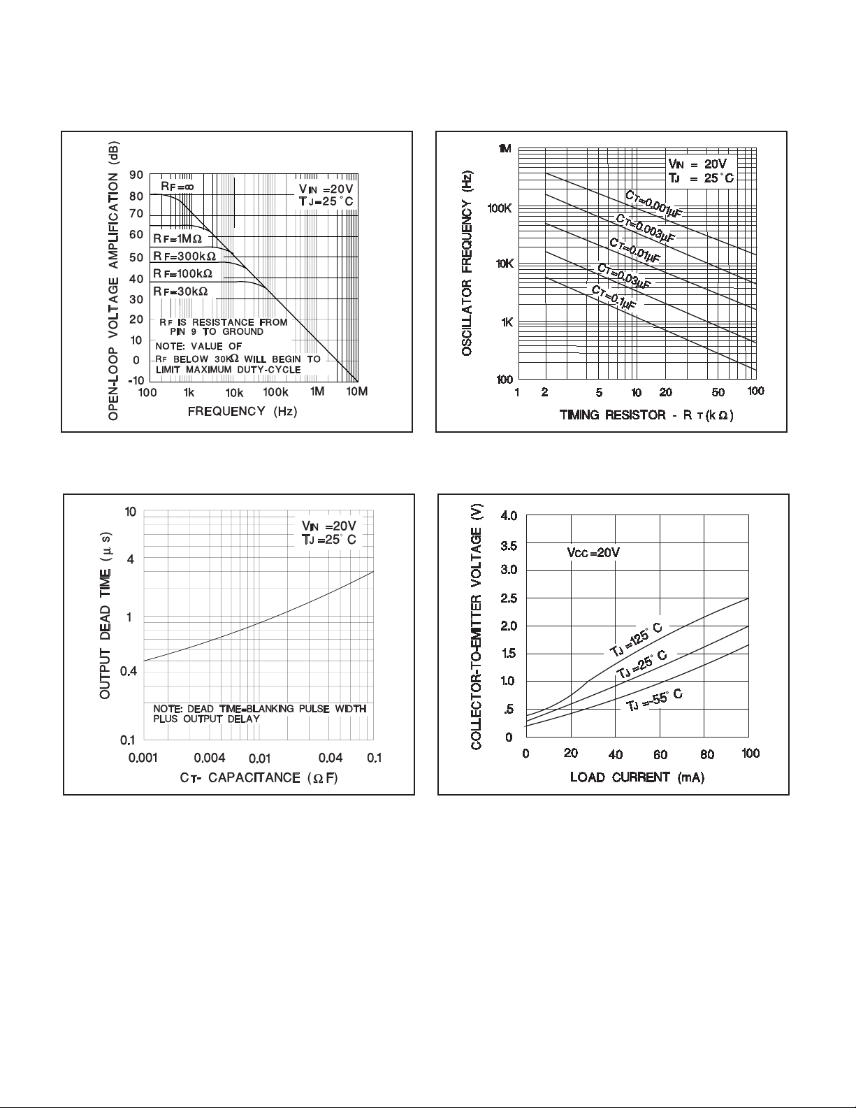
TYPICAL CHARACTERISTICS
UC1524
UC2524
UC3524
Open-loop voltage amplification of error amplifier vs
frequency.
Oscillator frequency vs timing components.
Output saturation voltage vs load current.Output dead time vs timing capacitance value.
4

APPLICATION INFORMATION
Oscillator
The oscillator controls the frequency of the UC1524 and is
programmed by R
formula:
where RTis in kΩ
where C
T
where f is in kHz
Practical values of C
Practical values of R
This results in a frequency range typically from 120Hz to
500kHz.
and CTaccording to the approximate
T
1.18
f
′
RC
TT
is in mF
fall between 0.001mF and 0.1mF.
T
fall between 1.8kΩ and 100kΩ.
T
UC1524
UC2524
UC3524
amplifier. This can easily be done with the circuit in Fig
ure 1:
Synchronous Operation
When an external clock is desired, a clock pulse of ap
proximately 3V can be applied directly to the oscillator
output terminal. The impedance to ground at this point is
approximately 2kΩ. In this configuration R
selected for a clock period slightly greater than that of the
external clock.
If two or more UC1524 regulators are to operated synchro
nously, all oscillator output terminals should be tied to
gether, all C
terminals connected to single timing capacitor,
T
and the timing resistor connected to a single R
TCT
T
must be
, terminal.
-
-
-
-
Blanking
The output pulse of the oscillator is used as a blanking
pulse at the output. This pulse width is controlled by the
value of C
. If small values of CTare required for fre
T
quency control, the oscillator output pulse width may still
be increased by applying a shunt capacitance of up to
100pF from pin 3 to ground. If still greater dead-time is required, it should be accomplished by limiting the maximum duty cycle by clamping the output of the error
16
V
REF
1N916
-
COMP 5k9
GND
8
Figure 1. Error amplifier clamp.
The other R
terminals can be left open or shorted to V
T
Minimum lead lengths should be used between the C
minals.
T
REF
ter-
.
Figure 2. Single-ended LC switching regulator circuit.
5

V+
+28 V
5k
5k
0.1 F
0.1 F
2k
5k
1
2
5k
16
6
7CT
3OSCOUT
10 SD
15
VIN
UC1524
INV INPUT
NON INV INPUT
VREF
RT
CLSENSE(+)
CLSENSE(-)
GND
8
CA
EA
CB
EB
COMP
12
11
13
14
4
5
9
1k
1W
0.001 F
1k
1W
100
100
50 k
2N4150
2N4150
0.1
20T5T5T
20T
500 F
+
1500 F
UC1524
UC2524
UC3524
5V
5A
Figure 3. Push-pull transformer coupled circuit.
Figure 4. Open loop test circuit.
UNITRODE CORPORATION
7 CONTINENTAL BLVD. • MERRIMACK, NH 03054
TEL. (603) 424-2410 FAX (603) 424-3460
6

PACKAGE OPTION ADDENDUM
www.ti.com
8-Mar-2005
PACKAGING INFORMATION
Orderable Device Status
(1)
Package
Type
Package
Drawing
Pins Package
Qty
Eco Plan
UC1524J OBSOLETE CDIP J 16 None Call TI Call TI
UC1524J/80937 OBSOLETE CDIP J 16 None Call TI Call TI
UC1524J883B OBSOLETE CDIP J 16 None Call TI Call TI
UC2524DW ACTIVE SOIC DW 16 40 None CU NIPDAU Level-2-220C-1 YEAR
UC2524DWTR ACTIVE SOIC DW 16 2000 None CU NIPDAU Level-2-220C-1 YEAR
UC2524J OBSOLETE CDIP J 16 None Call TI Call TI
UC2524N ACTIVE PDIP N 16 25 None CU SNPB Level-NA-NA-NA
UC3524D ACTIVE SOIC D 16 40 None CU NIPDAU Level-1-220C-UNLIM
UC3524DTR ACTIVE SOIC D 16 2500 None CU NIPDAU Level-1-220C-UNLIM
UC3524DW ACTIVE SOIC DW 16 40 None CU NIPDAU Level-2-220C-1 YEAR
UC3524DWTR ACTIVE SOIC DW 16 2000 None CU NIPDAU Level-2-220C-1 YEAR
UC3524J OBSOLETE CDIP J 16 None Call TI Call TI
UC3524N ACTIVE PDIP N 16 25 None CU SNPB Level-NA-NA-NA
(1)
The marketing status values are defined asfollows:
ACTIVE: Product device recommended for new designs.
LIFEBUY: TI has announced that the devicewill be discontinued, and a lifetime-buy period is in effect.
NRND: Not recommended for new designs. Device is in production to support existing customers, but TI does not recommend using this part in
a new design.
PREVIEW: Device has been announced but isnot in production. Samples may or may not be available.
OBSOLETE: TI has discontinued the production ofthe device.
(2)
Lead/Ball Finish MSL Peak Temp
(3)
(2)
Eco Plan - May not be currently available - please check http://www.ti.com/productcontent for the latest availability information and additional
product content details.
None: Not yet available Lead (Pb-Free).
Pb-Free (RoHS): TI's terms "Lead-Free" or "Pb-Free" mean semiconductor products that are compatible with the current RoHS requirements
for all 6 substances, including the requirement that lead not exceed 0.1% by weight in homogeneous materials. Where designed to be soldered
at high temperatures, TI Pb-Free products aresuitable for use in specified lead-free processes.
Green (RoHS & no Sb/Br): TI defines "Green" to mean "Pb-Free" and in addition, uses package materials that do not contain halogens,
including bromine (Br) or antimony (Sb) above0.1% of total product weight.
(3)
MSL, Peak Temp. -- The Moisture Sensitivity Level rating according to the JEDECindustry standard classifications, and peak solder
temperature.
Important Information and Disclaimer:The information provided on this page represents TI's knowledge and belief as of the date that it is
provided. TI bases its knowledge and belief on information provided by third parties, and makes no representation or warranty as to the
accuracy of such information. Efforts are underway to better integrate information from third parties. TI has taken and continues to take
reasonable steps to provide representative and accurate information but may not have conducted destructive testing or chemical analysis on
incoming materials and chemicals. TI and TI suppliers consider certain information to be proprietary, and thus CAS numbers and other limited
information may not be available for release.
In no event shall TI's liability arising out of such information exceed the total purchase price of the TI part(s) at issue in this document sold by TI
to Customer on an annual basis.
Addendum-Page 1

IMPORTANT NOTICE
Texas Instruments Incorporated and its subsidiaries (TI) reserve the right to make corrections, modifications,
enhancements, improvements, and other changes to its products and services at any time and to discontinue
any product or service without notice. Customers should obtain the latest relevant information before placing
orders and should verify that such information is current and complete. All products are sold subject to TI’s terms
and conditions of sale supplied at the time of order acknowledgment.
TI warrants performance of its hardware products to the specifications applicable at the time of sale in
accordance with TI’s standard warranty. Testing and other quality control techniques are used to the extent TI
deems necessary to support this warranty . Except where mandated by government requirements, testing of all
parameters of each product is not necessarily performed.
TI assumes no liability for applications assistance or customer product design. Customers are responsible for
their products and applications using TI components. To minimize the risks associated with customer products
and applications, customers should provide adequate design and operating safeguards.
TI does not warrant or represent that any license, either express or implied, is granted under any TI patent right,
copyright, mask work right, or other TI intellectual property right relating to any combination, machine, or process
in which TI products or services are used. Information published by TI regarding third-party products or services
does not constitute a license from TI to use such products or services or a warranty or endorsement thereof.
Use of such information may require a license from a third party under the patents or other intellectual property
of the third party, or a license from TI under the patents or other intellectual property of TI.
Reproduction of information in TI data books or data sheets is permissible only if reproduction is without
alteration and is accompanied by all associated warranties, conditions, limitations, and notices. Reproduction
of this information with alteration is an unfair and deceptive business practice. TI is not responsible or liable for
such altered documentation.
Resale of TI products or services with statements different from or beyond the parameters stated by TI for that
product or service voids all express and any implied warranties for the associated TI product or service and
is an unfair and deceptive business practice. TI is not responsible or liable for any such statements.
Following are URLs where you can obtain information on other Texas Instruments products and application
solutions:
Products Applications
Amplifiers amplifier.ti.com Audio www.ti.com/audio
Data Converters dataconverter.ti.com Automotive www.ti.com/automotive
DSP dsp.ti.com Broadband www.ti.com/broadband
Interface interface.ti.com Digital Control www.ti.com/digitalcontrol
Logic logic.ti.com Military www.ti.com/military
Power Mgmt power.ti.com Optical Networking www.ti.com/opticalnetwork
Microcontrollers microcontroller.ti.com Security www.ti.com/security
Telephony www.ti.com/telephony
Video & Imaging www.ti.com/video
Wireless www.ti.com/wireless
Mailing Address: Texas Instruments
Post Office Box 655303 Dallas, Texas 75265
Copyright 2005, Texas Instruments Incorporated
 Loading...