


NINA-W1 series
u-blox NINA-W1 series, NINA-W13 series, NINA-W15 series, NINA-W10 series, NINA-W101 System Integration Manual
...
NINA-W1 series
Stand-alone Wi-Fi and multiradio modules
System Integration Manual
Abstract
This document describes the system integration of NINA-W1 series stand-
alone modules, which
includes the NINA-W13 series (Wi-Fi) and NINA-W10 and NINA-W15 series (multiradio)
modules.
The module has a number of imp
ortant security features embedded, including secure boot, which
ensures that only authenticated software can run on the module. This makes NINA-
W1 ideal for
critical IoT applications where security is important. It connects to a host system using UART,
high-speed RMII, or a GPIO interface.
www.u-blox.com
UBX-17005730 - R07

NINA-W1 series - System Integration Manual
UBX-17005730 - R07 Page 2 of 47
Document Information
Title NINA-W1 series
Subtitle Stand-alone Wi-Fi and multiradio modules
Document type System Integration Manual
Document number UBX-17005730
Revision and date R07 18-Dec-2018
Disclosure Restriction
Product status
Corresponding content status
Functional Sample Draft For functional testing. Revised and supplementary data will be published later.
In Development /
Prototype
Objective Specification Target values. Revised and supplementary data will be published later.
Engineering Sample Advance Information Data based on early testing. Revised and suppleme ntary data will be published later.
Initial Production Early Production Information Data from product verification. Revised and supplementary data may be published later.
Mass Production /
End of Life
Production Information Document contains the final product specification.
This document applies to the following products:
Product name Type number
u-blox connectivity
software version
Hardware
version
PCN reference Product status
NINA-W131 NINA-W131-00B-00 1.0.0 06 N/A Initial Production
NINA-W131-00B-01 1.0.1 06 UBX-18016827 Initial Production
NINA-W131-01B-00 2.0.0 06 N/A Initial Production
NINA-W132 NINA-W132-00B-00 1.0.0 06 N/A Initial Production
NINA-W132-00B-01 1.0.1 06 UBX-18016827 Initial Production
NINA-W132-01B-00 2.0.0 06 N/A Initial Production
NINA-W101 NINA-W101-00B-00 - 06 N/A Initial Production
NINA-W102 NINA-W102-00B-00 - 06 N/A Initial Production
NINA-W151 NINA-W151-00B-00 1.0.0 06 N/A In Development
NINA-W152 NINA-W152-00B-00 1.0.0 06 N/A In Development
u-blox or third parties may hold intellectual property rights in the products, names, logos and designs included in this
document. Copying, reproduction, modification or disclosure to third parties of this document or any part thereof is only
permitted with the
express written permission of u-blox.
The information contained herein is provided “as is” and u
-blox assumes no liability for its use. No warranty, either express or
implied, is given, including but not limited
to, with respect to the accuracy, correctness, reliability and fitness for a particular
purpose of the information. This document may be revised by u
-blox at any time without notice. For the most recent
documents, visit www.u
-blox.com.
Copyright © u
-blox AG.

NINA-W1 series - System Integration Manual
UBX-17005730 - R07 Page 3 of 47
Contents
Document Information ................................................................................................................................ 2
Contents .......................................................................................................................................................... 3
System description ............................................................................................................................... 5
1.1 Overview ........................................................................................................................................................ 5
1.2 Architecture ................................................................................................................................................. 6
1.2.1 Block diagrams .................................................................................................................................... 6
1.3 CPU................................................................................................................................................................. 7
1.4 Operating modes ......................................................................................................................................... 7
1.4.1 Power modes ....................................................................................................................................... 7
1.5 Supply interfaces ........................................................................................................................................ 8
1.5.1 Module supply design (VCC) ............................................................................................................. 8
1.5.2 Digital I/O interfaces reference voltage (VCC_IO) ........................................................................ 8
1.5.3 VCC application circuits .................................................................................................................... 8
1.6 System function interfaces ...................................................................................................................... 8
1.6.1 Boot strapping pins ............................................................................................................................ 8
1.7 Data Interfaces ............................................................................................................................................ 9
1.7.1 Universal asynchronous serial interface (UART) ......................................................................... 9
1.7.2 Ethernet (RMII+SMI) ........................................................................................................................10
1.8 Antenna interfaces ...................................................................................................................................11
1.8.1 Antenna pin – NINA-W101/W131/W151 .....................................................................................11
1.8.2 Integrated antenna – NINA-W102/W132/W152 .......................................................................12
1.9 Reserved pins (RSVD) ..............................................................................................................................12
1.10 GND pins .....................................................................................................................................................12
Software ................................................................................................................................................. 13
2.1 Flashing the NINA module .......................................................................................................................13
2.2 Updating the NINA-W13/W15 u-blox connectivity software ..........................................................13
2.3 Developing and flashing the NINA-W10 open CPU software ..........................................................14
2.3.1 Setup Toolchain ................................................................................................................................14
2.3.2 Get ESP-IDF .......................................................................................................................................15
2.3.3 Setup path to ESP-IDF .....................................................................................................................16
2.3.4 Building and flashing ........................................................................................................................16
2.3.5 Automatic bootloader on NINA-W10 EVK ...................................................................................19
2.4 Arduino support for NINA-W10 ..............................................................................................................19
2.4.1 Downloading the Arduino IDE .........................................................................................................19
2.4.2 Downloading from the GIT repository ...........................................................................................20
2.4.3 Downloading the Toolchain ............................................................................................................21
2.5 Output power configuration ...................................................................................................................24
2.5.1 NINA-W10 series ..............................................................................................................................24
2.5.2 NINA-W13/W15 series ....................................................................................................................26
Design-in ................................................................................................................................................. 27

NINA-W1 series - System Integration Manual
UBX-17005730 - R07 Page 4 of 47
3.1 Overview ......................................................................................................................................................27
3.2 Supply interfaces ......................................................................................................................................27
3.2.1 Module supply (VCC) design ...........................................................................................................27
3.2.2 Digital I/O interfaces reference voltage (VCC_IO) ......................................................................27
3.3 Antenna interface .....................................................................................................................................28
3.3.1 RF transmission line design (NINA-W101/W131/W151) ........................................................28
3.3.2 Antenna design (NINA-W101/W131/W151) ..............................................................................30
3.3.3 On-board antenna design (NINA-W102/W132/W152 only) ....................................................33
3.4 Data communication interfaces ............................................................................................................34
3.4.1 Asynchronous serial interface (UART) design ............................................................................34
3.4.2 Ethernet (RMII+SMI) ........................................................................................................................34
3.5 General High Speed layout guidelines ..................................................................................................34
3.5.1 General considerations for schematic design and PCB floor-planning .................................34
3.5.2 Module placement ............................................................................................................................35
3.5.3 Layout and manufacturing .............................................................................................................35
3.6 Module footprint and paste mask .........................................................................................................35
3.7 Thermal guidelines ...................................................................................................................................36
3.8 ESD guidelines ...........................................................................................................................................36
Handling and soldering ...................................................................................................................... 37
4.1 Packaging, shipping, storage and moisture preconditioning ..........................................................37
4.2 Handling ......................................................................................................................................................37
4.3 Soldering .....................................................................................................................................................37
4.3.1 Reflow soldering process ................................................................................................................37
4.3.2 Cleaning ..............................................................................................................................................38
4.3.3 Other remarks ...................................................................................................................................39
Approvals ............................................................................................................................................... 40
5.1 General requirements ..............................................................................................................................40
5.2 FCC/IC End-product regulatory compliance ........................................................................................40
5.2.1 NINA-W10 series FCC ID and IC certification number ..............................................................40
5.2.2 NINA-W13/W15 series FCC ID and IC certification number ....................................................40
5.2.3 Antenna requirements ....................................................................................................................41
Product testing ................................................................................................................................... 42
6.1 u-blox In-Series production test .............................................................................................................42
6.2 OEM manufacturer production test .....................................................................................................42
6.2.1 “Go/No go” tests for integrated devices ......................................................................................43
Appendix ....................................................................................................................................................... 44
A Glossary ................................................................................................................................................. 44
Related documents ................................................................................................................................... 46
Revision history .......................................................................................................................................... 46
Contact ........................................................................................................................................................... 47

NINA-W1 series - System Integration Manual
UBX-17005730 - R07 System description Page 5 of 47
System description
1.1 Overview
The NINA-W1 series is a stand-alone Wireless and multiradio MCU IoT module suitable for industrial
markets where security is important. The NINA-W1 series includes the following tree variants as
listed in the table below:
Model Description
NINA-W13 series
Wireless MCU mod
ule that integrates a powerful microcontroller (MCU) and a radio for wireless
communication. The NINA-W13x modules come with pre-
flashed application software, supporting
802.11b/g/n in the 2.4 GHz ISM band. The host system can set up and control the module
through the AT
command interface. This greatly reduces the time and complexity to add Wi-Fi and Bluetooth
connectivity
to the end product. The NINA-
W13x modules provide top grade security, thanks to secure boot, which
ensures the module boots up only with original u-blox software.
NINA-W15 series
The NINA-W15x modules has similar performance as the NINA-W13x modules
but provides support for
dual-mode Bluetooth (Bluetooth BR/EDR low energy v4.2) making it a multiradio gateway.
NINA-W10 series
Multiradio
MCU module that integrates a powerful microcontroller (MCU) and a radio for wireless
communication. With the open CPU architecture, customers can develop advanced applications running
on the dual core 32-bit MCU. The radio provides support for Wi-Fi 802.1
1b/g/n in the 2.4 GHz ISM band,
Bluetooth BR/EDR, and Bluetooth low energy communication. The module can be used to design solutions
with top grade security, thanks to integrated cryptographic hardware accelerators. This enables secure
boot, which ensures the module boots up only in the presence of authenticated software.
NINA-W1 modules have full modular approval for Europe (RED), US (FCC), Canada (IC / ISED RSS),
Japan (MIC), Taiwan (NCC), South Korea (KCC), Australia / New Zealand (ACMA)
1
, Brazil (Anatel) 1,
South Africa (ICASA)
1
. The modules will be qualified for professional grade operation, supporting an
extended temperature range of -40 °C to +85 °C.
1
Approvals are pending.

NINA-W1 series - System Integration Manual
UBX-17005730 - R07 System description Page 6 of 47
1.2 Architecture
1.2.1 Block diagrams
Figure 1: Block diagram of NINA-W13 series
Figure 2: Block diagram of NINA-W15 series
Flash (16Mbit)
Linear voltage regulators
RF
ROM
Wi
-Fi
baseband
IO Buffers
2xXtensa 32-bit LX6 MCU
SRAM (4Mbit)
Cryptographics
hardware
accelerations
Antenna
(NINA-W132)
PLL
Quad SPI
VCC_IO
VCC (3.0
-3.6V)
40 MHz
Reset
UART
RMII
EFUSE
GPIO
BPF
ANT (NINA-
W131)
Flash (16Mbit)
Linear voltage regulators
RF
ROM
Wi-Fi baseband
IO Buffers
2xXtensa 32-bit LX6 MCU
SRAM (4Mbit)
Cryptographics
hardware
accelerations
Antenna
(NINA-W152)
PLL
Quad SPI
VCC_IO
VCC (3.0
- 3.6V)
40 MHz
Reset
UART
RMII
EFUSE
GPIO
BPF
ANT (NINA-
W151)
Bluetooth
baseband

NINA-W1 series - System Integration Manual
UBX-17005730 - R07 System description Page 7 of 47
Figure 3: Block diagram of NINA-W10 series
1.3 CPU
The NINA-W1 series has a dual-core system with two Harvard Architecture Xtensa LX6 CPUs with
maximum 240 MHz internal clock frequency. The internal memory of NINA-W1 includes the
following:
• 448 Kbyte ROM for booting and core functions
• 520 Kbyte SRAM for data and instruction
• 16 Mbit FLASH for code storage including hardware encryption to protect programs and data
• 1 kbit EFUSE (non- erasable memory) for MAC addresses, module configuration, Flash-
Encryption, and Chip-ID
The open CPU variants (NINA-W101/NINA-W102) also support external FLASH and SRAM memory
via a Quad SPI interface (see section 2.7.2.4).
1.4 Operating modes
1.4.1 Power modes
The NINA-W1 series modules are power efficient devices capable of operating in different power
saving modes and configurations. Different sections of the module can be powered off when not
needed and complex wake up events can be generated from different external and internal inputs.
For the lowest current consumption modes, an external LPO clock is required (available for NINAW10 series modules).
Flash (16Mbit)
Linear voltage regulators
RF
ROM
Wi-Fi baseband
Bluetooth
Baseband
IO Buffers
2xXtensa 32-bit LX6 MCU
S
RAM (4Mbit)
Cryptographics
hardware
accelerations
Antenna
(NINA-W102)
PLL
Quad SPI
V
CC_IO
VCC (3.0- 3.6V)
40 MHz
Reset
ANT (NINA-W10
1)
UART
RMII
I
2
C
SPI
SDIO
Quad SPI
JTAG
GPIO
ADC/DAC
EFUSE
CAN
BPF

NINA-W1 series - System Integration Manual
UBX-17005730 - R07 System description Page 8 of 47
1.5 Supply interfaces
1.5.1 Module supply design (VCC)
The NINA-W1 series modules use an integrated Linear Voltage converter to transform the supply
voltage presented at the VCC pin into a stable system voltage.
1.5.2 Digital I/O interfaces reference voltage (VCC_IO)
All modules in the NINA-W1 series provide an additional voltage supply input for setting the I/O
voltage level.
The separate VCC_IO pin enables integration of the module in many applications with different
voltage levels (for example, 1.8 V or 3.3 V) without any level converters. The NINA-W1 modules
support only 3.3 V as IO voltage level currently.
1.5.3 VCC application circuits
The power for the NINA-W1 series modules is provided through the VCC pins, which can be one of
the following:
• Switching Mode Power Supply (SMPS)
• Low Drop Out (LDO) regulator
The SMPS is the ideal choice when the available primary supply source has higher value than the
operating supply voltage of the NINA-W1 series modules. The use of SMPS provides the best power
efficiency for the overall application and minimizes current drawn from the main supply source.
⚠ While selecting SMPS, ensure that AC voltage ripple at switching frequency is kept as low as
possible. Layout shall be implemented to minimize impact of high frequency ringing.
The use of an LDO linear regulator is convenient for a primary supply with a relatively low voltage
where the typical 85-90% efficiency of the switching regulator leads to minimal current saving.
Linear regulators are not recommended for high voltage step-down as they will dissipate a
considerable amount of energy.
DC/DC efficiency should be evaluated as a tradeoff between active and idle duty cycle of the specific
application. Although some DC/DC can achieve high efficiency at extremely light loads, a typical
DC/DC efficiency quickly degrades as idle current drops below a few mA greatly reducing the battery
life.
It is considered as a best practice to have decoupling capacitors on the supply rails close to the
NINA-W1 series module, although depending on the design of the power routing on the host system,
capacitance might not be needed.
See the NINA-W13 series Data Sheet [2] and NINA-W10 series Data Sheet [3] for electrical
specifications.
1.6 System function interfaces
1.6.1 Boot strapping pins
There are several boot configuration pins available on the module that must have the correct
settings during boot. It is important that they are in the default state (marked with bold in Table 1)
during startup for normal operation. The default state is automatically selected (with internal pullups or pull-downs) if the pins are left unconnected.

NINA-W1 series - System Integration Manual
UBX-17005730 - R07 System description Page 9 of 47
Pin State during boot Default Behavior Description
36
0
VDD_SDIO=
3.3V
Voltage of Internal Flash
1
10
kΩ pull-up
VDD_SDIO=1
.8V
(VDD_SDIO should always be 1.8 V)
27, 25
00 Download Boot
Booting Mode, see
section 2 for information
about software upgrade.
01 Reserved, do not use
10
Pull-up*, Pull-down
*
Normal Boot from internal Flash
11
Normal Boot from internal Flash
32
0
Silent
Debugging Log on
U0TXD during booting
1
Pull-up* U0TXD Toggling
32, 28
00
Falling-edge input, falling-edge output
Timing of SDIO Slave
01
Falling-edge input, rising-edge output
10
Rising-edge input, falling-edge output
11
Pull-up*, Pull-up
*
Rising-edge input, rising-edge output
☞
*
About 30 kΩ
Table 1: NINA-W1 series boot strapping pins
1.7 Data Interfaces
1.7.1 Universal asynchronous serial interface (UART)
The NINA-W1 series module provides three Universal Asynchronous Serial Interface (UART) for data
communication. The following UART signals are available:
• Data lines (RXD as input, TXD as output)
• Hardware flow control lines (CTS as input, RTS as output)
• DSR and DTS are used to set and indicate the system modes
The UART can be used as 4-wire UART with hardware flow control and 2-wire UART with only TXD
and RXD.
If the UART is used in 2-wire mode, CTS should be connected to the GND on the NINA-W1 module.
The UART interface is also be used for firmware upgrade. See the Software section for more
information.
The u-blox connectivity software adds the DSR and DTR pins to the UART interface. These pins are
not used as originally intended, but to control the state of the NINA module. Depending on the
current configuration, the DSR can be used to:
• Enter command mode
• Disconnect and/or toggle connectable status
• Enable/disable the rest of the UART interface
• Enter/wake up from the sleep mode
The functionality of the DSR and DTR pins are configured by AT commands. See the u-blox Short
Range Modules AT commands manual [1]
for more information.
See NINA-W13 series Data Sheet [2], NINA-W10 series Data Sheet [3], and NINA-W15 series Data
Sheet [4] for characteristic information about the UART interface.
Interface Default configuration
UART interface 115200 baud, 8 data bits, no parity, 1 stop bit, hardware flow control
Table 2: Default settings for the UART port while using the u-blox connectivity software
NINA-W1 series - System Integration Manual
UBX-17005730 - R07 System description Page 10 of 47
It is recommended to make the UART0 available either as test points or connected to a header for
firmware upgrade. The IO level of the UART will follow the VCC_IO.
1.7.2 Ethernet (RMII+SMI)
For NINA-W13, RMII is supported from software version 2.0.0 onwards.
For NINA-W15, direct MAC to MAC connection will be supported when the module reaches
Engineering Sample status.
The NINA-W1 series module includes a full RMII for Ethernet MAC to PHY communication using the
included Station Management Interface (SMI). The RMII and SMI use 9 signals in total. The interface
requires an external 50 MHz clock source either from a compatible PHY chip or from an external
oscillator. The NINA-W1 series module cannot provide this clock signal by itself.
The two-wire SMI is used to configure the PHY chip. It uses a clock line and a data line to setup the
internal registers on PHY chip.
Due to pin muxing of the RMII interface, there is a limitation in the functionality of NINA-W13/W15
series module when using RMII. The following functions will be turned off when RMII communication
is initiated:
• Red, Green and Blue LED will be disabled
• UART will be run without flow control as CTS and RTS functionality will be disabled
• DSR and DTR functionality will be disabled
A pull up resistor of 1.5 kΩ must be added to MDIO pin.
1.7.2.1 Startup precautions
The RMII_CLK input (GPIO27) is muxed with the boot pin and must be held high 1.2 ms after the
reset signal is released to ensure not to enter the boot mode.
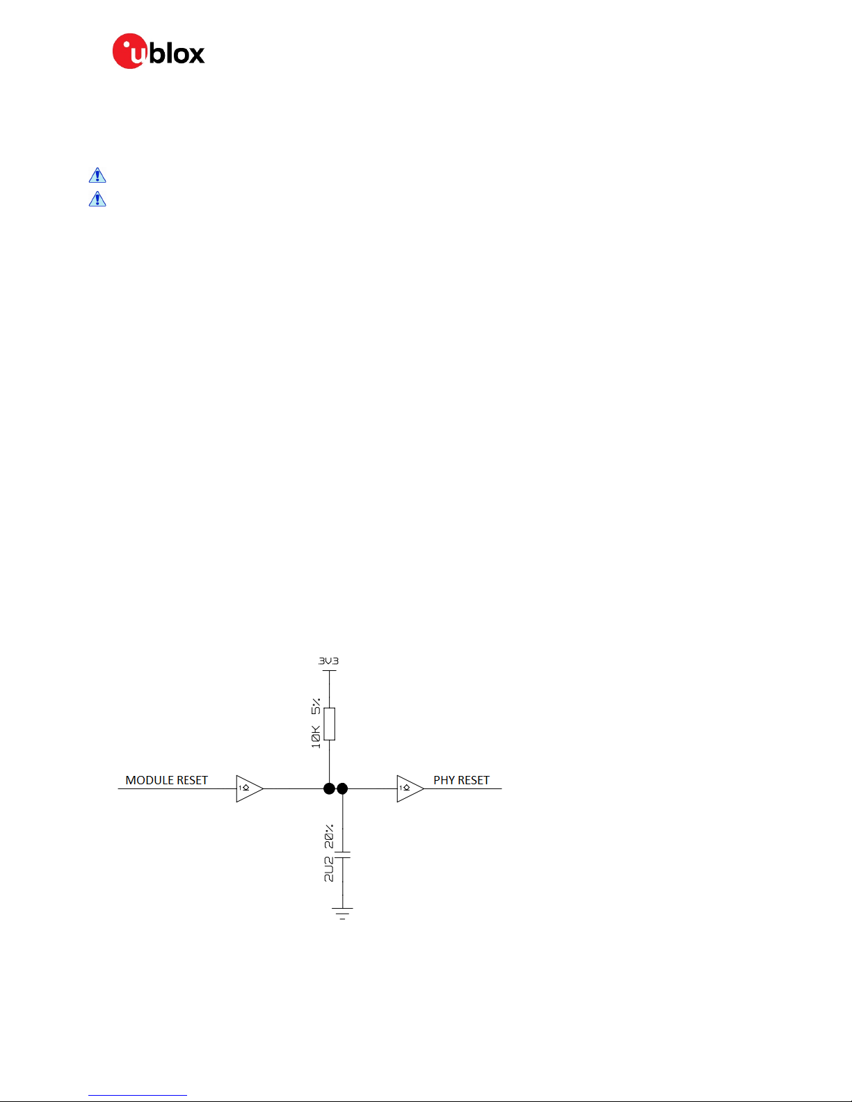
EVK-NINA-W1 uses two buffers and a low pass filter to delay the reset signal going to the PHY
circuit. See Figure 4.
This will delay the clock so that it starts a short time after the module is released from reset.
Figure 4: Delay circuit for RMII clock
Also the u-blox connectivity software will sense the RMII_CLK input (GPIO27) at startup. If an RMII
clock is discovered, then Ethernet communication will be initiated.
NINA-W1 series - System Integration Manual
UBX-17005730 - R07 System description Page 11 of 47
During startup of the NINA-W13/W15 series module, the RMII clock must be started within 100 us
but not before the initial delay of 1.2 ms.
1.7.2.2 MAC to PHY connection
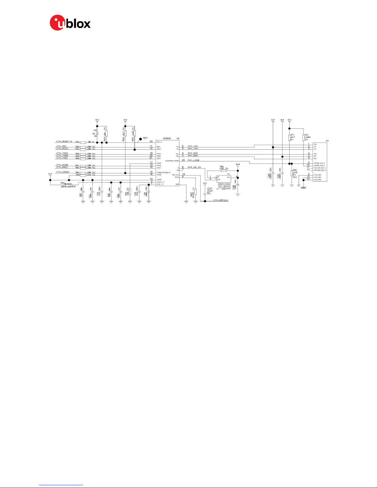
When connecting the NINA-W1 series module to an external PHY circuit, both the RMII and SMI
interfaces must be connected. The default PHY address (0x1) must be configured on the PHY side.
Follow the recommendations from the selected PHY chip for implementation details.
An example of a PHY implementation is shown in Figure 5. The PHY KSZ8081 is the recommended
PHY that is used on the EVK-NINA-W1.
Figure 5: Ethernet PHY implementation on the EVK-NINA-W1
1.7.2.3 MAC to MAC connection
If you connect the NINA-W1 series module using a direct MAC to MAC connection, the SMI interface
can be left unconnected. Depending on the routing of the RMII interface on the host PCB,
termination resistors might also be needed.
An external 50 MHz oscillator is needed while running a MAC to MAC connection.
1.8 Antenna interfaces
The antenna interface is different for each module variant in the NINA-W1 series.
1.8.1 Antenna pin – NINA-W101/W131/W151
The NINA-W101/W131/W151 modules are equipped with an RF pin. The RF pin has a nominal
characteristic impedance of 50 Ω and must be connected to the antenna through a 50 Ω
transmission line to allow reception of radio frequency (RF) signals in the 2.4 GHz frequency band.
Choose an antenna with optimal radiating characteristics for the best electrical performance and
overall module functionality. An internal antenna, integrated on the application board or an external
antenna that is connected to the application board through a proper 50 Ω connector can be used.
While using an external antenna, the PCB-to-RF-cable transition must be implemented using either
a suitable 50 Ω connector, or an RF-signal solder pad (including GND) that is optimized for 50 Ω
characteristic impedance.
1.8.1.1 Antenna matching
The antenna return loss should be as good as possible across the entire band when the system is
operational to provide optimal performance. The enclosure, shields, other components, and
surrounding environment will impact the return loss seen at the antenna port. Matching
components are often required to retune the antenna to bring the return loss within an acceptable
range.

NINA-W1 series - System Integration Manual
UBX-17005730 - R07 System description Page 12 of 47
It is difficult to predict the actual matching values for the antenna in the final form factor. Therefore,
it is a good practice to have a placeholder in the circuit with a ”pi” network, with two shunt
components and a series component in the middle, to allow maximum flexibility while tuning the
matching to the antenna feed.
1.8.1.2 Approved antenna designs
NINA-W1 modules come with a pre-certified design that can be used to save costs and time during
the certification process. To take advantage of this service, you have to implement the antenna
layout according to the u-blox reference designs. The reference design is available on request from
u-blox.
The designer integrating a u-blox reference design into an end-product is solely responsible for the
unintentional emission levels produced by the end product.
The module may be integrated with other antennas. In this case, the OEM installer must certify his
design with respective regulatory agencies.
1.8.2 Integrated antenna – NINA-W102/W132/W152
The NINA-W102/W132/W152 modules are equipped with an integrated antenna on the module for
simpler integration.
1.9 Reserved pins (RSVD)
RSVD pins should be left unconnected.
1.10 GND pins
Good connection of the module's GND pins with solid ground layer of the host application board is
required for correct RF performance. It significantly reduces the EMC issues and provides a thermal
heat sink for the module.

NINA-W1 series - System Integration Manual
UBX-17005730 - R07 Software Page 13 of 47
Software
The NINA-W13/W15 series module is delivered with the u-blox connectivity software.
The u-blox connectivity software enables the use of Wi-Fi, Bluetooth and Bluetooth low energy,
controlled by the AT commands over the UART interface. More information on the features and
capabilities of the u-blox connectivity software and how to use it can be found in the
u-blox Short
Range Modules AT Commands Manual [1] and NINA-W1 Getting Started [6].
The NINA-W10 series module is delivered without any software flashed.
2.1 Flashing the NINA module
The NINA-W13 and NINA-W15 application can be flashed using the s-center (XMODEM protocol is
used). The following pins should be made available as either headers or test points to flash the
module:
• UART (RXD, TXD, CTS, RTS)
• Bootstrap pins 25 and 27
• Reset_n
• SWITCH_1 and SWITCH_2
2.2 Updating the NINA-W13/W15 u-blox connectivity software
The u-blox connectivity software for NINA-W13/W15 is designed to validate the hardware,
bootloader, and the binary image itself to make sure it runs only on a validated hardware such as
NINA-W13/W15.
The u-blox connectivity software is delivered in a zip file – “NINA-W1xX_SW1.0.0.zip”.
Unzip this file before downloading. The secure boot is included in the file – *.json.
In s-center software, secure boot is supported from version 4.7 onwards. The *.json-file should be
selected to make to use secure boot in the s-center as shown in Figure 6.
The s-center will handle the download using the information in the *.json file. No other interaction is
needed from the user.
To manually start the download using a software other than s-center, use the following AT
command to start updating the NINA-W13/W15 u-blox connectivity software:
AT+UFWUPD=<mode>,<baud>,<image id>,<image size>,<base64 encoded signature>,<image
name>,<flags>
Sample parameters that can be used while doing the flash update is provided below:
AT+UFWUPD=0,115200,0,651840,jzlRIkg37ir/pVpDKVrPot2ZdsaNvUtSYP2pDAUVJc7iQI9yzIo8V
Fv8C1olP/9I4UJ4WmgC5oRay4AC0V8jRJSFFX/wop6x/sBJGOeDEu7yC/s0+Oj7CLs4TzNbiRqK0zLwKR
iHohgVyzWqhwKFpmcxcDXphjkCTIvpffY8TwDLzkowuuD59R+sQCueJtBHBg9KDB3TOs8bsXLaVtT2x1r
LfMg8/pb+BPQEK9NcNB4hbp693ATivYE3cmxzWykIjEje819SIRGhHFt0wAsqh7WFgSJYNgDi5cLdOYz+
r1+j7+l4RqrMl/A/QYyWS9z0Q15QcJ3GlAJlXYa5v/ISjA==,nina-w1-debug,rwx
When a ‘C’ character is received from NINA-W13/W15, the XMODEM download is ready to begin
from the host.

NINA-W1 series - System Integration Manual
UBX-17005730 - R07 Software Page 14 of 47
Figure 6: Software Update using s-center
For more information about the parameters, see the Software update +UFWUPD command in u-blox
Short Range Modules AT Commands Manual [1] and NINA-W1 Getting Started [6].
2.3 Developing and flashing the NINA-W10 open CPU software
If you are using the NINA-W10 open CPU variant, it is not possible to use the u-blox connectivity
software. Use the software developed and compiled using the Espressif SDK on this variant.
The build and flash information while using Espressif SDK is available at the following URL -
http://esp-idf.readthedocs.io/en/latest/get-started/index.html.
This URL provides information on how to set up the software environment using the hardware based
on the Espressif ESP32 such as NINA-W10 and also how to use the ESP-IDF (Espressif IoT
Development Framework).
The following must be setup in order to compile, flash, and execute a program on NINA-W10:
• Setup Toolchain
o Windows, Mac, and Linux is supported
• Get ESP-IDF
o Download the GIT repository provided by Espressif
• Setup Path to ESP-IDF
o The toolchain program can access the ESP-IDF using IDF_PATH environment variable
• Build and Flash
o Start a Project, Connect, Configure, Build and Flash a program
More information about this is available at - http://esp-idf.readthedocs.io/en/latest/index.html
2.3.1 Setup Toolchain
To start development with ESP32, it is recommended to use a prebuilt toolchain. Currently,
Windows, Mac, and Linux is supported. The example in this document will use a Toolchain for
running Windows, that is, a bash shell window. The toolchain contains all programs and compiler to
build an application.
The latest toolchain for Windows can be downloaded from
https://dl.espressif.com/dl/esp32_win32_msys2_environment_and_toolchain-20170918.zip
Unzip the file to c:\ msys32. This path is assumed in the following examples, but it can be located in
another folder as well. The file size is around 500 MB.

NINA-W1 series - System Integration Manual
UBX-17005730 - R07 Software Page 15 of 47
Start the bash shell using the“mingw32.exe” (“mingw64.exe” is currently not supported).
☞ If you encounter any issues, use the “autorebase.bat” and the “msys2_shell.cmd” shortcuts. This
will reset the path variable with a Cygwin installation on some computers, which can have
problems with the path to the compiler or the python tool.
2.3.2 Get ESP-IDF
The source files for Espressif ESP-IDF repository is located on github at
https://github.com/espressif/esp-idf.
To download the files, open the “mingw32.exe”, navigate to the directory where you want to have the
ESP-IDF (like c:\git), and clone it using “git clone” command.
☞ Use the “--recursive” parameter
In this example, the esp-idf repository will be created in the c:\git folder.
git clone --recursive https://github.com/espressif/esp-idf.git
To checkout a specific tag such as v2.1, use the following command as shown in the example below:
git clone https://github.com/espressif/esp-idf.git esp-idf-v3.1
cd esp-idf-v3.1/
git checkout v3.1
git submodule update --init --recursive
Figure 7: Example of the git clone of ESP-IDF
Go to the new folder by typing “cd esp-idf” and then type “ls” to show the folder content.
cd esp-idf
ls
 Loading...