


MAX-7C-0
Ublox MAX-7C-0, MAX-7Q-0, NEO-7M-0, NEO-7P-0, MAX-7W-0 Manual
...
Abstract
This document describes the features and specifications of the cost
effective and high-performance MAX-7 and NEO-7
GPS/GLONASS/QZSS modules featuring the u-blox 7 positioning
engine.
These compact, easy to integrate stand-alone GNSS receiver
modules combine exceptional GNSS performance with highly
flexible power, design, and connectivity options. Their compact
form factors and SMT pads allow fully automated assembly with
standard pick & place and reflow soldering equipment for costefficient, high-volume production enabling short time-to-market.
www.u-blox.com
UBX-13003704 - R09
MAX-7 / NEO-7
u-blox 7 GNSS modules
Hardware Integration Manual
MAX-7 / NEO-7 - Hardware Integration Manual
Document Information
Title
MAX-7 / NEO-7
Subtitle
u-blox 7 GNSS modules
Document type
Hardware Integration Manual
Document number
UBX-13003704
Revision and date
R09
26-Sep-2017
Document status
Production Information
Document status explanation
Objective Specification
Document contains target values. Revised and supplementary data will be published later.
Advance Information
Document contains data based on early testing. Revised and supplementary data will be published later.
Early Production Information
Document contains data from product verification. Revised and supplementary data may be published later.
Production Information
Document contains the final product specification.
European Union regulatory compliance
Product name
Type number
ROM/FLASH version
PCN reference
MAX-7C-0
All
ROM1.00
MAX-7Q-0
All
ROM1.00
MAX-7W-0
All
ROM1.00
NEO-7N-0
All
FLASH1.00
NEO-7M-0
All
ROM1.00
NEO-7P-0
All
FLASH1.01
u-blox reserves all rights to this document and the information contained herein. Products, names, logos and designs described herein
may in whole or in part be subject to intellectual property rights. Reproduction, use, modification or disclosure to third parties of this
document or any part thereof without the express permission of u-blox is strictly prohibited.
The information contained herein is provided “as is” and u-blox assumes no liability for the use of the information. No warranty, either
express or implied, is given, including but not limited, with respect to the accuracy, correctness, reliability and fitness for a particular
purpose of the information. This document may be revised by u-blox at any time. For most recent documents, visit www.u-blox.com.
Copyright © 2017, u-blox AG.
u-blox is a registered trademark of u-blox Holding AG in the EU and other countries
MAX-7 and NEO-7 complies with all relevant requirements for RED 2014/53/EU. The MAX-7 andNEO-7 Declaration of Conformity (DoC) is
available at www.u-blox.com within Support > Product resources > Conformity Declaration.
This document applies to the following products:
UBX-13003704 - R09 Production Information Page 2 of 52

MAX-7 / NEO-7 - Hardware Integration Manual
Preface
u-blox Technical Documentation
As part of our commitment to customer support, u-blox maintains an extensive volume of technical
documentation for our products. In addition to our product-specific technical data sheets, the following manuals
are available to assist u-blox customers in product design and development.
GPS Compendium: This document, also known as the GPS book, provides a wealth of information
regarding generic questions about GPS system functionalities and technology.
Receiver Description including Protocol Specification: Messages, configuration and functionalities of
the u-blox 7 software releases and positioning modules are explained in this document.
Hardware Integration Manuals: This manual provides hardware design instructions and information on
how to set up production and final product tests.
Application Note: These documents provide general design instructions and information that applies to all
u-blox GPS/GNSS positioning modules.
How to use this Manual
The MAX-7 and NEO-7 Hardware Integration Manual provides the necessary information to successfully design-
in and configure these u-blox 7-based positioning modules. This manual has a modular structure. It is not
necessary to read it from beginning to end.
The following symbols are used to highlight important information within the manual:
An index finger points out key information pertaining to module integration and performance.
A warning symbol indicates actions that could negatively influence or damage the module.
Questions
If you have any questions about u-blox 7 Hardware Integration, please:
Read this manual carefully.
Contact our information service on the homepage http://www.u-blox.com
Read the questions and answers on our FAQ database on the homepage http://www.u-blox.com
Technical Support
Worldwide Web
Our website (www.u-blox.com) is a rich pool of information. Product information, technical documents and
helpful FAQ are available 24h a day.
By E-mail
If you have technical problems or cannot find the required information in the provided documents, contact the
closest Technical Support office. To ensure that we process your request as soon as possible, use our service pool
email addresses rather than personal staff email addresses. Contact details are at the end of the document.
Helpful Information when Contacting Technical Support
When contacting Technical Support please have the following information ready:
Receiver type (e.g. NEO-7N-0-000), Datacode (e.g. 172100.0100.000) and firmware version (e.g. ROM1.0)
Receiver configuration
Clear description of your question or the problem together with a u-center logfile
A short description of the application
Your complete contact details
UBX-13003704 - R09 Production Information Preface
Page 3 of 52

MAX-7 / NEO-7 - Hardware Integration Manual
Contents
Preface ................................................................................................................................ 3
Contents .............................................................................................................................. 4
1 Quick reference ............................................................................................................ 7
2 Hardware description .................................................................................................. 8
2.1 Overview .............................................................................................................................................. 8
2.2 Architecture .......................................................................................................................................... 8
2.3 Operating modes .................................................................................................................................. 8
2.3.1 Continuous Mode ......................................................................................................................... 8
2.3.2 Power Save Mode ......................................................................................................................... 9
2.4 Configuration ....................................................................................................................................... 9
2.4.1 Electrical Programmable Fuse (eFuse) ............................................................................................. 9
2.5 Connecting power .............................................................................................................................. 10
2.5.1 VCC: Main supply voltage ........................................................................................................... 10
2.5.2 VCC_IO: IO supply voltage (MAX-7) ............................................................................................ 10
2.5.3 V_BCKP: Backup supply voltage .................................................................................................. 10
2.5.4 VDD_USB: USB interface power supply (NEO-7) ........................................................................... 11
2.5.5 VCC_RF: Output voltage RF section ............................................................................................. 11
2.5.6 V_ANT: Antenna supply (MAX-7W) ............................................................................................. 11
2.6 Interfaces ............................................................................................................................................ 11
2.6.1 UART ........................................................................................................................................... 11
2.6.2 USB ............................................................................................................................................. 11
2.6.3 Display Data Channel (DDC) ........................................................................................................ 12
2.6.4 SPI (NEO-7) .................................................................................................................................. 13
2.7 I/O pins ............................................................................................................................................... 13
2.7.1 RESET_N: Reset input .................................................................................................................. 13
2.7.2 EXTINT: External interrupt ............................................................................................................ 13
2.7.3 D_SEL: Interface select (NEO-7) .................................................................................................... 13
2.7.4 TX Ready signal ........................................................................................................................... 14
2.7.5 ANT_ON: Antenna ON (LNA enable) (NEO-7N, MAX-7Q, MAX-7C) ............................................. 14
2.7.6 Antenna Short circuit detection (MAX-7W) ................................................................................. 14
2.7.7 Antenna open circuit detection ................................................................................................... 14
2.7.8 Time pulse ................................................................................................................................... 14
3 Design ......................................................................................................................... 15
3.1 Design checklist .................................................................................................................................. 15
3.1.1 Schematic checklist ..................................................................................................................... 15
UBX-13003704 - R09 Production Information Contents
Page 4 of 52

MAX-7 / NEO-7 - Hardware Integration Manual
3.1.2 Layout checklist ........................................................................................................................... 15
3.1.3 Antenna checklist ........................................................................................................................ 16
3.2 Design considerations for minimal designs .......................................................................................... 16
3.2.1 Minimal design (NEO-7N) ............................................................................................................ 17
3.2.2 Minimal design (MAX-7Q) ........................................................................................................... 18
3.3 Layout ................................................................................................................................................ 19
3.3.1 Footprint and paste mask ............................................................................................................ 19
3.3.2 Placement ................................................................................................................................... 20
3.3.3 Antenna connection and ground plane design ............................................................................ 20
3.3.4 General design recommendations: .............................................................................................. 21
3.3.5 Antenna micro strip ..................................................................................................................... 22
3.4 Antenna and Antenna supervision ...................................................................................................... 23
3.4.1 Antenna design with passive antenna ......................................................................................... 23
3.4.2 Active antenna design without antenna supervisor (NEO-7N/7M/7P, MAX-7C/7Q) ...................... 24
3.4.3 Antenna design with active antenna using antenna supervisor (MAX-7W) .................................. 25
3.4.4 Design with GLONASS / GPS active antenna ................................................................................ 30
3.4.5 Design with GLONASS / GPS passive antenna .............................................................................. 31
3.5 Recommended parts ........................................................................................................................... 32
3.5.1 Recommended GPS & GLONASS active antenna (A1) .................................................................. 33
3.5.2 Recommended GPS & GLONASS passive patch antenna .............................................................. 33
3.5.3 Recommended GPS & GLONASS passive chip antenna ................................................................ 33
4 INPAQ (www.inpaq.com.tw) ..................................................................................... 34
5 5.2 x 3.7 x 0.7 mm GPS+GLONASS ............................................................................. 34
6 Migration to u-blox-7 modules ................................................................................. 35
6.1 Migrating u-blox 6 designs to a u-blox 7 module ................................................................................ 35
6.2 Hardware migration............................................................................................................................ 35
6.2.1 Hardware compatibility: .............................................................................................................. 35
6.2.2 Hardware migration NEO-6 -> NEO-7 .......................................................................................... 36
6.2.3 Hardware migration MAX-6 -> MAX-7 ........................................................................................ 37
6.3 Software migration ............................................................................................................................. 38
6.3.1 Software compatibility ................................................................................................................. 38
6.3.2 Messages no longer supported .................................................................................................... 38
7 Product handling ........................................................................................................ 39
7.1 Packaging, shipping, storage and moisture preconditioning ............................................................... 39
7.1.1 Population of Modules ................................................................................................................ 39
7.2 Soldering ............................................................................................................................................ 39
7.2.1 Soldering paste............................................................................................................................ 39
7.2.2 Reflow soldering ......................................................................................................................... 39
7.2.3 Optical inspection ........................................................................................................................ 40
7.2.4 Cleaning ...................................................................................................................................... 40
7.2.5 Repeated reflow soldering ........................................................................................................... 41
UBX-13003704 - R09 Production Information Contents
Page 5 of 52

MAX-7 / NEO-7 - Hardware Integration Manual
7.2.6 Wave soldering............................................................................................................................ 41
7.2.7 Hand soldering ............................................................................................................................ 41
7.2.8 Rework ........................................................................................................................................ 41
7.2.9 Conformal coating ...................................................................................................................... 41
7.2.10 Casting ........................................................................................................................................ 41
7.2.11 Grounding metal covers .............................................................................................................. 41
7.2.12 Use of ultrasonic processes .......................................................................................................... 42
7.3 EOS/ESD/EMI precautions ................................................................................................................... 42
7.3.1 Electrostatic discharge (ESD) ........................................................................................................ 42
7.3.2 ESD handling precautions ............................................................................................................ 42
7.3.3 ESD protection measures ............................................................................................................. 43
7.3.4 Electrical Overstress (EOS) ............................................................................................................ 43
7.3.5 EOS protection measures ............................................................................................................. 43
7.3.6 Electromagnetic interference (EMI) .............................................................................................. 44
7.3.7 Applications with cellular modules .............................................................................................. 45
8 Product testing ........................................................................................................... 47
8.1 u-blox in-series production test ........................................................................................................... 47
8.2 Test parameters for OEM manufacturer .............................................................................................. 47
8.3 System sensitivity test ......................................................................................................................... 47
8.3.1 Guidelines for sensitivity tests ...................................................................................................... 48
8.3.2 ‘Go/No go’ tests for integrated devices ........................................................................................ 48
A Appendix .................................................................................................................... 49
A.1 Abbreviations ..................................................................................................................................... 49
A.2 Design-in recommendations in combination with cellular operation ................................................... 50
Related documents........................................................................................................... 51
Revision history ................................................................................................................ 51
Contact .............................................................................................................................. 52
UBX-13003704 - R09 Production Information Contents
Page 6 of 52

MAX-7 / NEO-7 - Hardware Integration Manual
Layout
Power
Interfaces
I/Os
Antenna
See section 3.3
See sections 2.3 and 2.4
See section 2.6
See section 2.7
See sections 2.5.6 and 3.4
1 Quick reference
When using this manual for a design, make sure you also have the data sheet for the specific positioning module
(see Related documents).
For information about migration, see sections 4.2.3 (MAX-7) and 4.2.2 (NEO-7).
Table 1: Quick guide to this document
UBX-13003704 - R09 Production Information Quick reference
Page 7 of 52
MAX-7 / NEO-7 - Hardware Integration Manual
2 Hardware description
2.1 Overview
u-blox 7 modules are standalone GNSS positioning modules featuring the high performance u-blox 7 positioning
engine. Available in industry standard form factors in leadless chip carrier (LCC) packages, they are easy to
integrate and they combine exceptional positioning performance with highly flexible power, design, and
connectivity options. SMT pads allow fully automated assembly with standard pick & place and reflow-soldering
equipment for cost-efficient, high-volume production enabling short time-to-market.
For product features see the module data sheet.
To determine which u-blox product best meets your needs, see the product selector tables on the u-blox
website (www.u-blox.com).
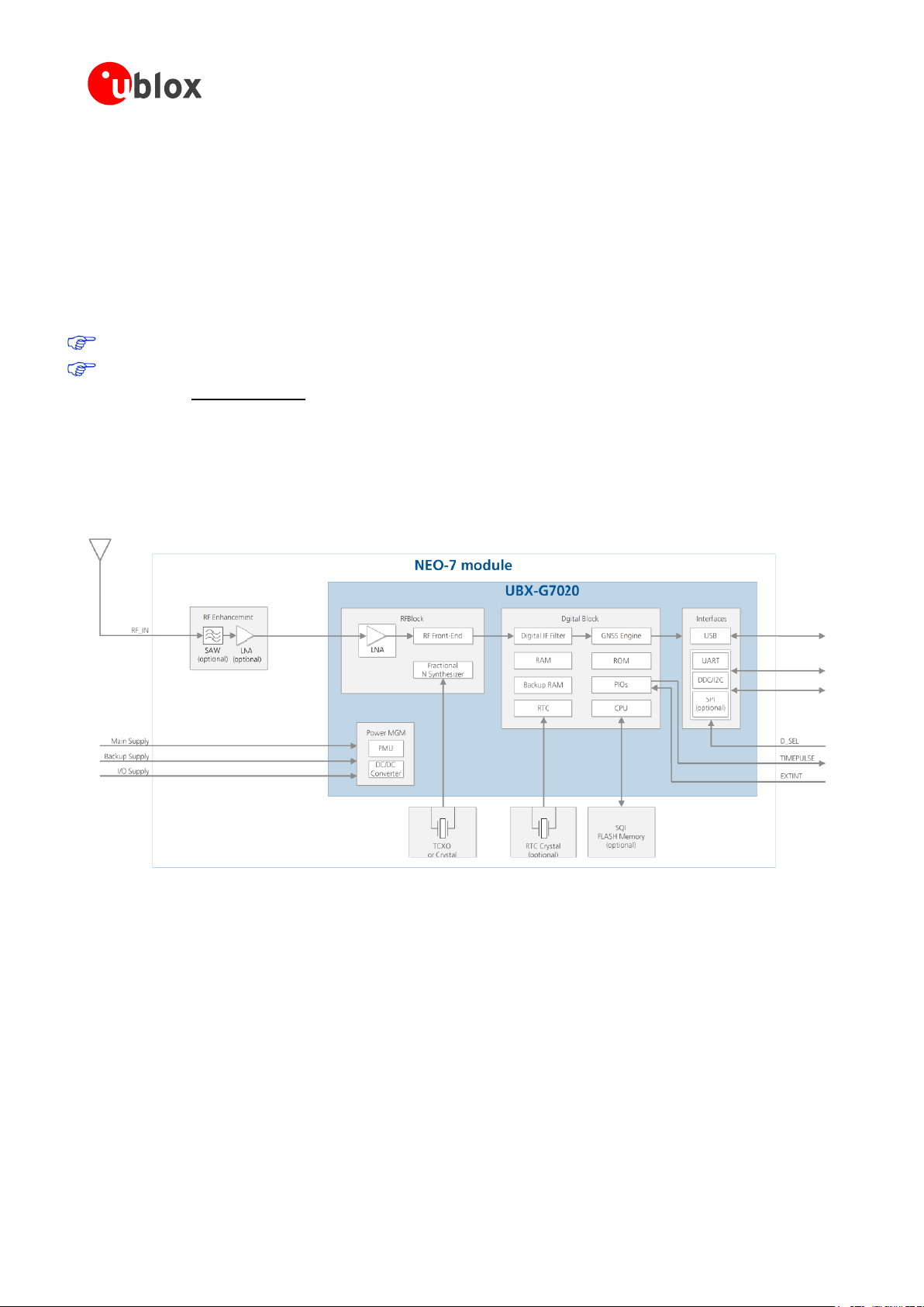
2.2 Architecture
u-blox 7 modules consist of two functional parts - the RF block and the digital block (see Figure 1).
The RF block includes the input matching elements, the SAW band pass filter, the integrated LNA and the
oscillator, while the digital block contains the u-blox 7 GNSS engine, the RTC crystal and additional elements
such as the optional FLASH Memory for enhanced programmability and flexibility.
Figure 1: u-blox-7 block diagram
2.3 Operating modes
u-blox receivers support different power modes. These modes represent strategies of how to control the
acquisition and tracking engines in order to achieve either the best possible performance or good performance
with reduced power consumption.
2.3.1 Continuous Mode
During a cold start, a receiver in Continuous Mode continuously deploys the acquisition engine to search for all
satellites. Once the receiver can calculate a position and track a sufficient number of satellites, the acquisition
engine powers off, resulting in significant power savings. The tracking engine continuously tracks acquired
satellites and acquires other available or emerging satellites. Whenever the receiver can no longer calculate a
position or the number of satellites tracked is below the sufficient number, the acquisition engine powers on
UBX-13003704 - R09 Production Information Hardware description
Page 8 of 52

MAX-7 / NEO-7 - Hardware Integration Manual
USB self powered / UART Baud Rate 1200
B5 62 06 41 09 00 01 01 30 81 00 00 00 00 FE 01 22
USB self powered / UART Baud Rate 2400
B5 62 06 41 09 00 01 01 30 81 00 00 00 00 FD 00 21
USB self powered / UART Baud Rate 4800
B5 62 06 41 09 00 01 01 30 81 00 00 00 00 FC FF 20
USB self powered / UART Baud Rate 9600
B5 62 06 41 09 00 01 01 30 81 00 00 00 00 FF 02 23
USB self powered / UART Baud Rate 19200
B5 62 06 41 09 00 01 01 30 81 00 00 00 00 FB FE 1F
USB self powered / UART Baud Rate 38400
B5 62 06 41 09 00 01 01 30 81 00 00 00 00 FA FD 1E
USB self powered / UART Baud Rate 57600
B5 62 06 41 09 00 01 01 30 81 00 00 00 00 F9 FC 1D
USB self powered / UART Baud Rate 115200
B5 62 06 41 09 00 01 01 30 81 00 00 00 00 F8 FB 1C
again to guarantee a quick reacquisition. Even if the acquisition engine powers off, the tracking engine
continues to acquire satellites.
For best performance, use continuous mode.
2.3.2 Power Save Mode
Two Power Save Mode (PSM) operations called ON/OFF and Cyclic tracking are available. These use different
ways to reduce the average current consumption in order to match the needs of the specific application. PSM
operations are set and configured using serial commands. For more information, see the u-blox 7 Receiver
Description Including Protocol Specification [4].
The system can shut down an optional external LNA using the ANT_ON signal in order to optimize power
consumption, see section 2.7.5.
Using the USB Interface is not recommended with Power Save Mode since the USB standard does not
allow a device to be non-responsive. Thus, it is not possible to have full advantage of Power Save Mode
operations in terms of saving current consumption.
Power Save Mode is not supported in GLONASS mode.
2.4 Configuration
The configuration settings can be modified using UBX protocol configuration messages. The modified settings
remain effective until power-down or reset. If these settings have been stored in BBR (Battery Backed RAM), then
the modified configuration will be retained, as long as the backup battery supply is not interrupted.
Configuration can be saved permanently in SQI flash.
2.4.1 Electrical Programmable Fuse (eFuse)
u-blox 7 includes an integrated eFuse memory for permanently saving configuration settings.
If no external FLASH memory is available, the eFuse memory can also be used to store the configuration. The
customer can program the eFuse.
eFuse is One-Time-Programmable; it cannot be changed if it has been programmed once.
String to change the default Baud rate:
UBX-13003704 - R09 Production Information Hardware description
Page 9 of 52

MAX-7 / NEO-7 - Hardware Integration Manual
USB bus powered / UART Baud Rate 1200
B5 62 06 41 09 00 01 01 30 81 00 00 00 00 F6 F9 1A
USB bus powered / UART Baud Rate 2400
B5 62 06 41 09 00 01 01 30 81 00 00 00 00 F5 F8 19
USB bus powered / UART Baud Rate 4800
B5 62 06 41 09 00 01 01 30 81 00 00 00 00 F4 F7 18
USB bus powered / UART Baud Rate 9600
B5 62 06 41 09 00 01 01 30 81 00 00 00 00 F7 FA 1B
USB bus powered / UART Baud Rate 19200
B5 62 06 41 09 00 01 01 30 81 00 00 00 00 F3 F6 17
USB bus powered / UART Baud Rate 38400
B5 62 06 41 09 00 01 01 30 81 00 00 00 00 F2 F5 16
USB bus powered / UART Baud Rate 57600
B5 62 06 41 09 00 01 01 30 81 00 00 00 00 F1 F4 15
USB bus powered / UART Baud Rate 115200
B5 62 06 41 09 00 01 01 30 81 00 00 00 00 F0 F3 14
To set the default Vendor or Vendor ID, you will need the specific string. To obtain the USB Vendor ID or USB
Vendor string, contact the the nearest Technical Support office by email. You will find the Contact details at
the end of the document.
2.5 Connecting power
u-blox 7 positioning modules have up to five power supply pins: VCC, VCC_IO, V_BCKP, V_ANT and
VDD_USB.
2.5.1 VCC: Main supply voltage
The VCC pin provides the main supply voltage. During operation, the current drawn by the module can vary by
some orders of magnitude, especially if enabling low-power operation modes. For this reason, it is important
that the supply circuitry be able to support the peak power (see datasheet for specification) for a short time.
Some u-blox 7 modules integrate a DC/DC converter. This allows reduced power consumption, especially when
using a main supply voltage above 2.5 V.
When switching from backup mode to normal operation or at start-up, u-blox 7 modules must charge the
internal capacitors in the core domain. In certain situations, this can result in a significant current draw.
For low power applications using Power Save and backup modes it is important that the power supply or
low ESR capacitors at the module input can deliver this current/charge.
Use a proper GND concept. Do not use any resistors or coils in the power line. For ground plane design
see section 3.3.3
2.5.2 VCC_IO: IO supply voltage (MAX-7)
VCC_IO from the host system supplies the digital I/Os. The wide range of VCC_IO allows seamless interfacing to
standard logic voltage levels independent of the VCC voltage level. In many applications, VCC_IO is simply
connected to the main supply voltage.
Without a VCC_IO supply, the system will remain in reset state.
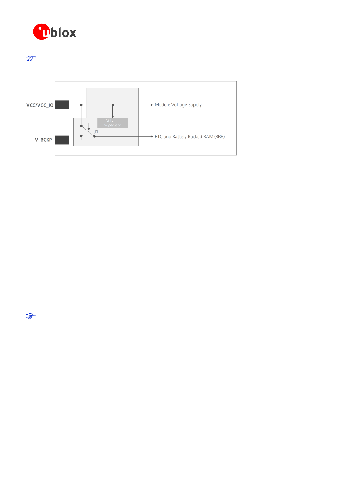
2.5.3 V_BCKP: Backup supply voltage
In case of a power failure on the module supply, the real-time clock (RTC) and battery backed RAM (BBR) are
supplied by V_BCKP. Use of valid time and the GNSS orbit data at start up will improve the GNSS performance
i.e. enables hot starts, warm starts, AssistNow Autonomous and AssistNow Offline. If no backup battery is
connected, the module performs a cold start at power up.
Avoid high resistance on the V_BCKP line: During the switch from main supply to backup supply a short
current adjustment peak can cause high voltage drop on the pin with possible malfunctions.
If no backup supply voltage is available, connect the V_BCKP pin to VCC_IO (or to VCC if not avaiable).
UBX-13003704 - R09 Production Information Hardware description
Page 10 of 52
MAX-7 / NEO-7 - Hardware Integration Manual
As long as the u-blox 7 module is supplied to VCC and VCC_IO, the backup battery is disconnected from
the RTC and the BBR to avoid unnecessary battery drain (see Figure 2). In this case, VCC supplies power to
the RTC and BBR.
Figure 2: Backup battery and voltage (for exact pin orientation, see data sheet)
2.5.3.1 RTC derived from the system clock; “Single Crystal” feature (MAX-7C)
On MAX-7C, the reference frequency for the RTC clock can be internally derived from the crystal system clock
frequency (26 MHz) when in Hardware Backup Mode. This feature is called “single crystal” operation. The
backup battery supplies the crystal via V_BCKP in the event that VDD_IO fails to provide power to derive and
maintain the RTC clock. This makes MAX-7C a more cost efficient solution, at the expense of a higher backup
current, compared to the usage of an ordinary RTC crystal on other MAX-7 variants. The capacity of the backup
battery at V_BCKP must be increased accordingly if Hardware Backup Mode is needed.
2.5.4 VDD_USB: USB interface power supply (NEO-7)
VDD_USB supplies the USB interface. If the USB interface is not used, the VDD_USB pin must be connected to
GND. For more information about correctly handling the VDD_USB pin, see section 2.6.2.1.
2.5.5 VCC_RF: Output voltage RF section
The VCC_RF pin can supply an active antenna or external LNA. For more information, see section 3.4.3.2.
2.5.6 V_ANT: Antenna supply (MAX-7W)
The V_ANT pin is available to provide antenna bias voltage to supply an optional external active antenna. For
more information, see section 3.4.3.2.
If not used, connect the V_ANT pin to GND.
2.6 Interfaces
2.6.1 UART
u-blox 7 positioning modules include a Universal Asynchronous Receiver Transmitter (UART) serial interface
RxD/TxD supporting configurable baud rates. The baud rates supported are specified in the u-blox 7 Receiver
Description Including Protocol Specification [4]
The signal output and input levels are 0 V to VCC for NEO-7 and 0 V to VCC_IO for MAX-7 modules. An
interface based on RS232 standard levels (+/- 12 V) can be implemented using level shifters such as Maxim
MAX3232. Hardware handshake signals and synchronous operation are not supported.
2.6.2 USB
A USB version 2.0 FS (Full Speed, 12 Mb/s) compatible interface is available for communication as an alternative
to the UART. The USB_DP integrates a pull-up resistor to signal a full-speed device to the host. The VDD_USB
pin supplies the USB interface.
UBX-13003704 - R09 Production Information Hardware description
Page 11 of 52
MAX-7 / NEO-7 - Hardware Integration Manual
Name
Component
Function
Comments
U1
LDO
Regulates VBUS (4.4 …5.25 V)
down to a voltage of 3.3 V.
Almost no current requirement (~1 mA) if the GNSS receiver is operated as a
USB self-powered device, but if bus-powered LDO (U1) must be able to deliver
the maximum current. For the peak supply current, see a low-cost DC/DC
converter such as LTC3410 from Linear Technology.
C23,
C24
Capacitors
Required according to the specification of LDO U1
D2
Protection
diodes
Protect circuit from overvoltage
/ ESD when connecting.
Use low capacitance ESD protection such as ST Microelectronics USBLC6-2.
R4, R5
Serial
termination
resistors
Establish a full-speed driver
impedance of 28…44
A value of 27 is recommended.
R11
Resistor
1 k is recommended for USB self-powered setup. For bus-powered setup,
R11 can be ignored.
u-blox provides Microsoft® certified USB drivers for Windows XP, Windows Vista, and Windows 7 operating
systems (also Windows 8 compatible). These drivers are available at www.u-blox.com.
2.6.2.1 USB external components
The USB interface requires some external components to implement the physical characteristics required by the
USB 2.0 specification. These external components are shown in Figure 3 and listed in Table 2. To comply with
USB specifications, VBUS must be connected through an LDO (U1) to pin VDD_USB on the module.
If the USB device is self-powered, the power supply (VCC) can be turned off and the digital block is not
powered. In this case, since VBUS is still available, the USB host would still receive the signal indicating that the
device is present and ready to communicate. This should be avoided by disabling the LDO (U1) using the enable
signal (EN) of the VCC-LDO or the output of a voltage supervisor. Depending on the characteristics of the LDO
(U1) it is recommended to add a pull-down resistor (R11) at its output to ensure VDD_USB is not floating if the
LDO (U1) is disabled or the USB cable is not connected i.e. VBUS is not supplied.
If the device is bus-powered, LDO (U1) does not need an enable control.
Figure 3: USB Interface
Table 2: Summary of USB external components
2.6.3 Display Data Channel (DDC)
An I2C compatible Display Data Channel (DDC) interface is available with u-blox 7 modules for serial
communication with an external host CPU. The interface only supports operation in slave mode (master mode is
not supported). The DDC protocol and electrical interface are fully compatible with the Fast-Mode of the I2C
industry standard. DDC pins SDA and SCL have internal pull-up resistors.
For more information about the DDC implementation, see the u-blox 7 Receiver Description Including Protocol
Specification [4]. For bandwidth information, see the Data Sheet. For timing, parameters consult the I2C-bus
specification [9].
The u-blox 7 DDC interface supports serial communication with u-blox cellular modules. See the
specification of the applicable cellular module to confirm compatibility.
With u-blox 7, when reading the DDC internal register at address 0xFF (messages transmit buffer), the
master must not set the reading address before every byte is accessed, as this could cause a faulty
UBX-13003704 - R09 Production Information Hardware description
Page 12 of 52
MAX-7 / NEO-7 - Hardware Integration Manual
Pin
D_SEL pin open
D_SEL pin low
18
DDC Data
SPI CS_N
19
DDC Clock
SPI SCK
20
TxD
SPI MISO
21
RxD
SPI MOSI
behavior. After every byte is read from register 0xFF the internal address counter is incremented by one,
saturating at 0xFF. Therefore, subsequent reads can be performed continuously.
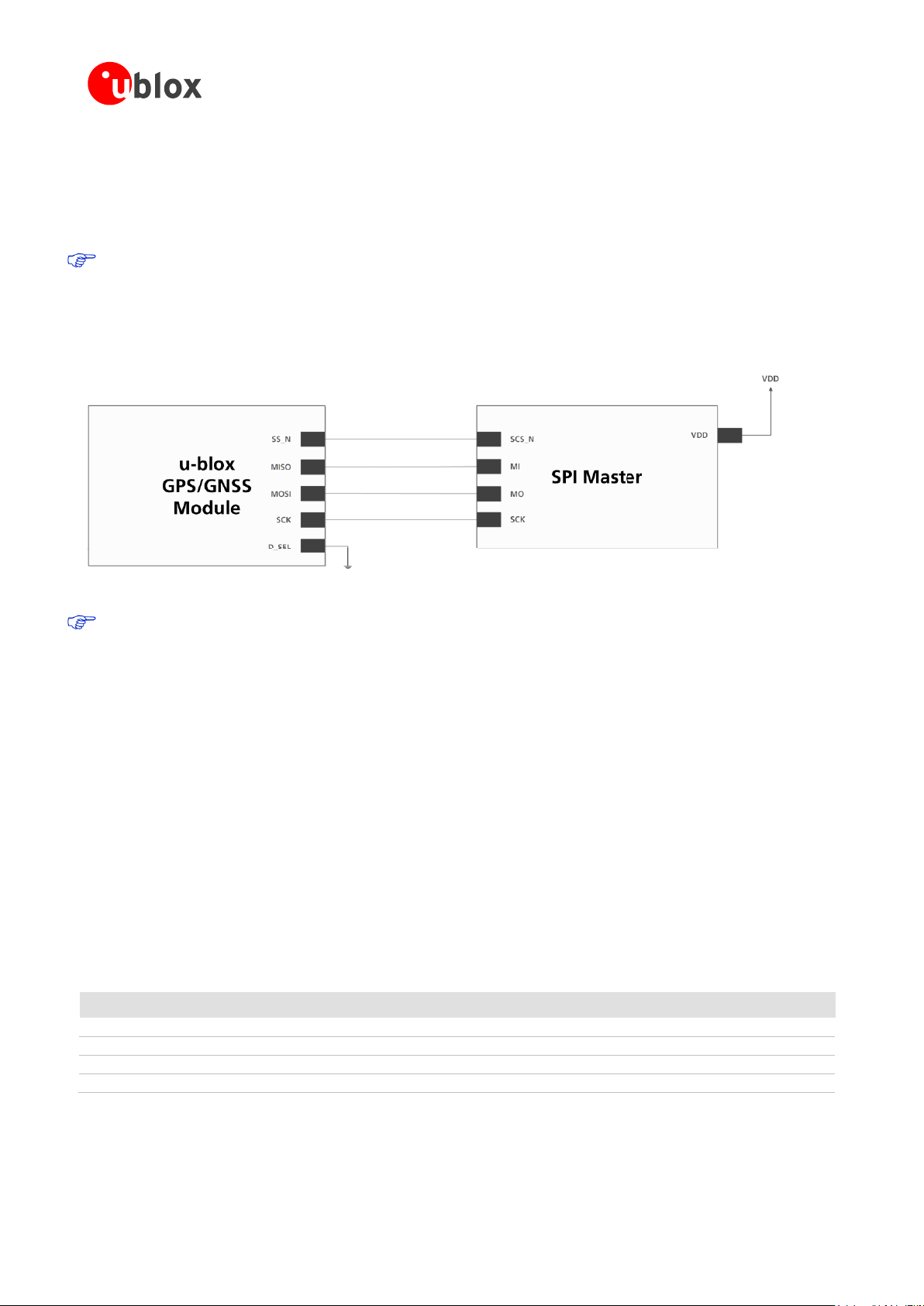
2.6.4 SPI (NEO-7)
With NEO-7 modules, an SPI interface is available for communication to a host CPU.
SPI is not available in the default configuration, because its pins are shared with the UART and DDC
interfaces. The SPI interface can be enabled by connecting D_SEL to ground (NEO-7) (see section 2.7.3).
For speed and clock frequency see the Data Sheet.
Figure 4 shows how to connect a u-blox GNSS receiver to a host/master. The signal on the pins must meet the
conditions specified in the Data Sheet.
Figure 4: Connecting to SPI Master
VCC_IO must have the same voltage level as the host.
2.7 I/O pins
2.7.1 RESET_N: Reset input
Driving RESET_N low activates a hardware reset of the system. Use this pin only to reset the module. Do not use
RESET_N to turn the module on and off, since the reset state increases power consumption. With u-blox 7
RESET_N is an input only.
2.7.2 EXTINT: External interrupt
EXTINT is an external interrupt pin with fixed input voltage thresholds with respect to VCC or VCC_IO (see the
data sheet for more information). It can be used for wake-up functions in Power Save Mode on all u-blox 7
modules and for aiding. Leave open if unused.
2.7.3 D_SEL: Interface select (NEO-7)
The D_SEL pin, available on all NEO-7 modules, selects the available interfaces. SPI cannot be used
simultaneously with UART/DDC.
If open, UART and DDC are available. If pulled low, the SPI Interface is available.
Table 3: D_SEL pin on NEO-7
UBX-13003704 - R09 Production Information Hardware description
Page 13 of 52

MAX-7 / NEO-7 - Hardware Integration Manual
2.7.4 TX Ready signal
The TX Ready signal indicates that the receiver has data to transmit. A listener can wait on the TX Ready signal
instead of polling the DDC or SPI interfaces. The UBX-CFG-PRT message lets you configure the polarity and the
number of bytes in the buffer before the TX Ready signal goes active. The TX Ready signal can be mapped to
UART TXD (PIO 06). The TX Ready function is disabled by default.
The TX-ready functionality can be enabled and configured by proper AT commands sent to the involved
u-blox cellular module supporting the feature. For more information see GPS Implementation and Aiding
Features in u-blox wireless modules [10].
2.7.5 ANT_ON: Antenna ON (LNA enable) (NEO-7N, MAX-7Q, MAX-7C)
In Power Save Mode, the system can turn on/off an optional external LNA using the ANT_ON signal in order to
optimize power consumption. A pull-down resistor (10 kOhm) is required to ensure correct operation in backup
mode of the ANT_ON signal.
2.7.6 Antenna Short circuit detection (MAX-7W)
The MAX-7W module includes internal short circuit antenna detection. For more information, see section
3.4.3.2.
2.7.7 Antenna open circuit detection
2.7.7.1 Antenna open circuit detection (MAX-7)
Antenna open circuit detection (OCD) is not activated by default on the MAX-7 module. OCD can be mapped to
PIO13 (EXTINT). For more information about how to implement OCD, see section 3.4.3.3. To learn how to
configure OCD see the u-blox 7 Receiver Description including Protocol Specification [4].
2.7.8 Time pulse
A configurable time pulse signal is available with all u-blox 7 modules. By default, the time pulse signal is
configured to 1 pulse per second. For more information see the u-blox 7 Receiver Description including Protocol
Specification [4].
UBX-13003704 - R09 Production Information Hardware description
Page 14 of 52
MAX-7 / NEO-7 - Hardware Integration Manual
3 Design
3.1 Design checklist
Designing-in a u-blox 7 module is easy, especially when based on a u-blox reference design. Nonetheless, it pays
to do a quick sanity check of the design. This section lists the most important items for a simple design check.
The design checklist can also help to avoid an unnecessary PCB respin and achieve the best possible
performance. Follow the design checklists when developing any u-blox 7 GNSS applications. This can
significantly reduce development time and costs.
3.1.1 Schematic checklist
If required, does your schematic allow for using different module variants? See the u-blox website
(www.u-blox.com) to compare the available features of u-blox 7 GNSS modules.
Plan the use of a second interface (Test points on UART, DDC or USB) for firmware updates or as a
service connector.
Power supply requirements
GNSS positioning modules require a stable power supply. In selecting a strategy to achieve a clean and
stable power supply, any resistance in the VCC supply line can negatively influence performance.
Consider the following points:
Wide power lines or even power planes are preferred.
Avoid resistive components in the power line (e.g. narrow power lines, coils, resistors, etc.).
Placing a filter or other source of resistance at VCC can create significantly longer acquisition times.
For ground plane design, see section 3.3.3.
Are all power supplies (VCC, VDD_USB) within the specified range? (See the data sheet: NEO-7 [1] or
MAX-7 [2])
Compare the peak supply current consumption of your u-blox 7 module with the specification of the
power supply. (See the data sheet for more information.)
At the module input, use low ESR capacitors that can deliver the required current/charge for switching
from backup mode to normal operation.
Backup battery
Use of valid time and the GNSS orbit data at startup will improve the GNSS performance i.e. enables hot
starts, warm starts and the AssistNow Autonomous process as well as AssistNow Offline. To make use of
these features connect a battery to V_BCKP to continue supplying the backup domain in case of power
failure at VCC_IO.
If no backup supply voltage is available, connect the V_BCKP pin to VCC_IO (or to VCC if not avaiable).
3.1.2 Layout checklist
See section 3.3.
Is the GNSS module located according to the recommendation?
Has the grounding concept been followed?
Has the micro strip been kept as short as possible?
Add a ground plane underneath the GNSS module to reduce interference.
For improved shielding, add as many vias as possible around the micro strip, around the serial
communication lines, underneath the GNSS module etc.
Have appropriate EOS/ESD/EMI protection measures been included? This is especially important for
designs including cellular modules.
UBX-13003704 - R09 Production Information Design
Page 15 of 52

MAX-7 / NEO-7 - Hardware Integration Manual
3.1.3 Antenna checklist
The total noise figure should be well below 3 dB.
If a patch antenna is the preferred antenna, choose a patch of at least 15x15x4 mm for standalone
GPS/QZSS, or choose a patch of at least 25x25x4 mm for GPS + GLONASS. For smaller antennas, an LNA
with a noise figure <2 dB is recommended. (MAX-7Q, NEO-7N)
Make sure the antenna is not placed close to noisy parts of the circuitry. (E.g. micro-controller, display,
etc.)
To optimize performance in environments with out-of band jamming sources, use an additional SAW
filter.
The micro strip must be 50 and be routed in a section of the PCB where minimal interference from
noise sources can be expected.
In case of a multi-layer PCB, use the thickness of the dielectric between the signal and the first GND layer
(typically the 2nd layer) for the micro strip calculation.
If the distance between the micro strip and the adjacent GND area (on the same layer) does not exceed 5
times the track width of the micro strip, use the “Coplanar Waveguide” model in AppCad to calculate
the micro strip and not the “micro strip” model see section 3.3.5
Use an external LNA if your design does not include an active antenna when optimal performance is
important.
For information on ESD protection for patch antennas and removable antennas, see section 5.3.3 and if
you use GPS for design in combination with GSM or other radio then check sections 5.3.5 to 5.3.7.
For more information dealing with interference, issues see the GPS Antenna Application Note [6].
3.2 Design considerations for minimal designs
For a minimal design with a u-blox 7 GNSS module, the following functions and pins need consideration:
Connect the Power supply to VCC.
Connect VCC_IO to VCC or to the corresponding voltage.
Assure an optimal ground connection to all ground pins of the module.
Connect the antenna to RF_IN over a 50 line and define the antenna supply (V_ANT) for active antennas
(internal or external power supply).
Choose the required serial communication interface (UART, USB, SPI or DDC) and connect the appropriate
pins to your application.
If you need improved start-up or use AssistNow Autonomous in your application, connect a backup supply
voltage to V_BCKP.
For active antenna design, see section 3.4.2.
UBX-13003704 - R09 Production Information Design
Page 16 of 52
 Loading...