

Page 1

Horizontal-Deflection
Output Transistors
PRODUCT GUIDE
Page 2
1
Outline
Toshiba has developed a range of fifth-generation horizontal-deflection-output transistors (HV-Trs). Radical redesign of
the emitter electrode and the contact pattern has yielded significant improvements, resulting in higher current density
and superior electrical characteristics compared to those of fourth-generation products. Toshiba’s propriety glassmesa structure results in a high breakdown voltage.
Thanks to Toshiba’s wealth of experience and the wide variety of products which the company can offer, Toshiba
horizontal-deflection-output transistors are used World-wide in color TVs and video display monitors.
2
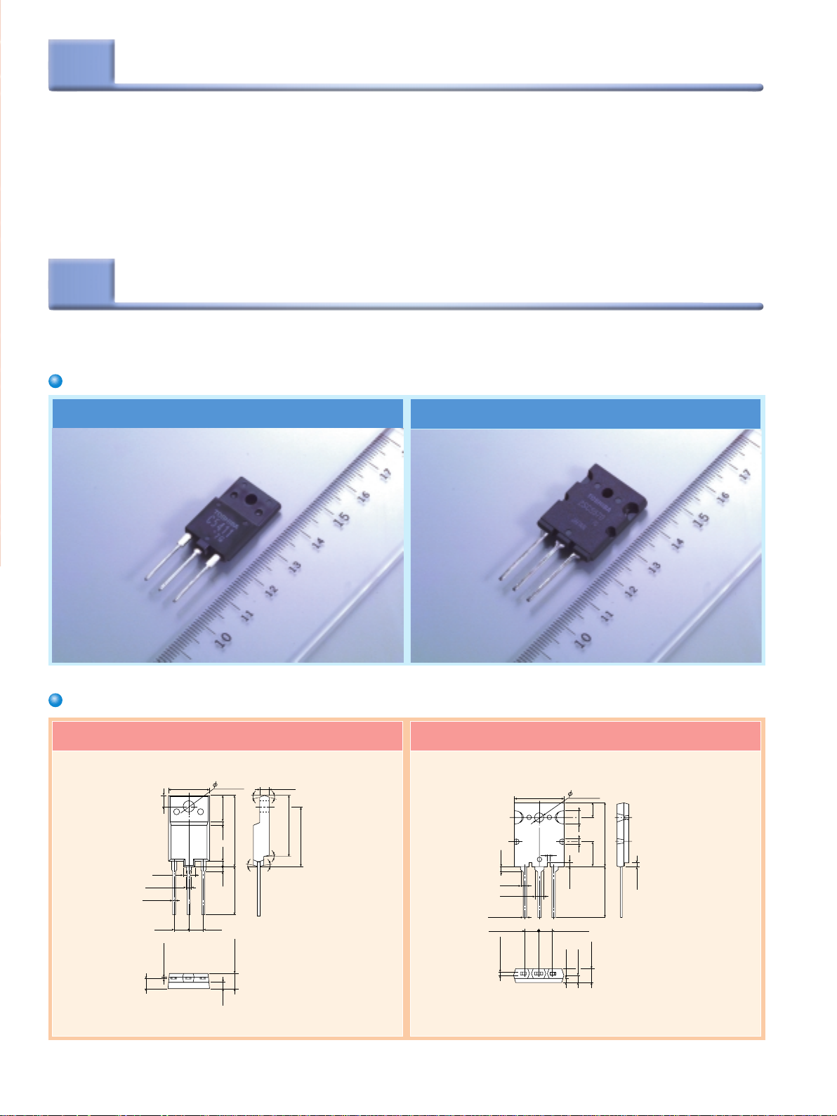
Appearance, Package and Weight
The photographs below show the products and their markings. The packages shown are is the straight-lead
packages used for standard products.
Appearance
TO-3P(H)IS TO-3P(LH)
2SC5411
5.5g ( typ. )
2SC5570
9.75g ( typ. )
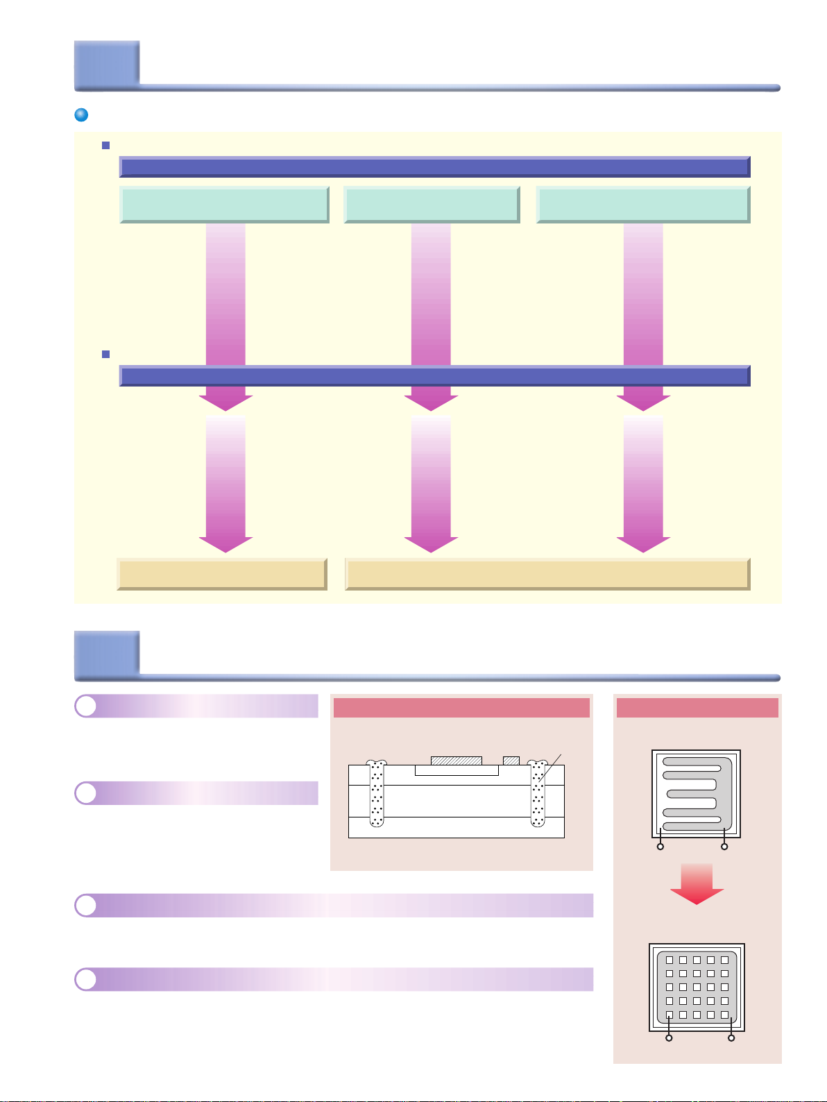
Package dimensions
3.6 ± 0.3 3.0 ± 0.315.5 ± 0.5
4.0
2.3 max
0.95 max
5.45
+ 0.25
3.3
4.5
0.9 – 0.1
123
10.0
1.2
2.5 2.0
5.45
2.0
26.5 ± 0.5
5˚
16.4 min
5.5 ± 0.3
10˚
1. Base
2. Collector
3. Emitter
(Unit : mm)
TO-3P(LH)TO-3P(H)IS
10˚
23.0
22.0 ± 0.5
5˚
5˚
20.5 max 3.3 ± 0.2
2.5
3.0
123
1.5
1.5
1.5
2.50
+ 0.3
1.0 – 0.25
5.45 ± 0.15 5.45 ± 0.15
– 0.10
+ 0.25
0.6
6.0
± 0.5
4.0
26.0
2.0
11.0
± 0.6
20.0
5.2 max
2.8
1. Base
2. Collector (heat sink)
3. Emitter
2.0
3
Page 3
3
BE
BE
Device Trends
Market trends and the development of horizontal-deflection output transistors
Device Trends
Market requirements
TV
Wide-screen TVs
Wide-screen
•
aspect ratio: (4 : 3) –> (16 : 9)
Large screen size
•
Flat screen
•
Low loss
•
Lower prices
•
Development of Horizontal-Deflection Output Transistors
HDTVs / Projectors
Multimedia-compatible TVs
Digital TV
Improved in screen resolution quality
•
Screen resolution: 525p, 1125i, 780p
Progressive system is improved
Starting grand wave digital
broadcasting
Various appllications such as
DVDs and Cable TVs
Various screen size
•
Flat screen
•
Low loss
•
Emitter contact shape and chip size optimization
Enhancement of 1700 V
•
product line
Low price due to reduction in
•
chip size
Fourth generation of horizontal-
deflection output transistors
Development of 2000-V products
•
Development of products incorporating
•
diodes for use in digital TVs
Shorter t
•
•
V
•
TO-3P(H)IS packages
21-A products available
•
rr
Reduced saturation voltage
(sat) = 3 V (max)
CE
High-current devices housed in
Reduced variation in product characteristics
Fifth generation of horizontal-deflection
s
output transistors
Video display monitors
High horizontal frequency
•
21 inches f
Large screen size
•
Standard size: 15 inches –> 17 inches
Low price
•
Reduced part count
(driving circuit and resonating capacitor are fixed)
Low loss
•
Flat screen
•
Reduced switching loss (tf parts) due to
•
high-frequency operation tf = 150 ns (max)
Reduced saturation voltage at high currents
•
V
CE
High-current devices housed in
•
TO-3P(H)IS packages
21-A products available
Increased allowable power dissipation
•
TO-3P(H) IS 65 W –> 75 W
TO-3P(LH) 200 W –> 220 W
Reduced variation in product characteristics
•
= 120 kHz –> 135 kHz
H
(sat) = 3 V (max)
4
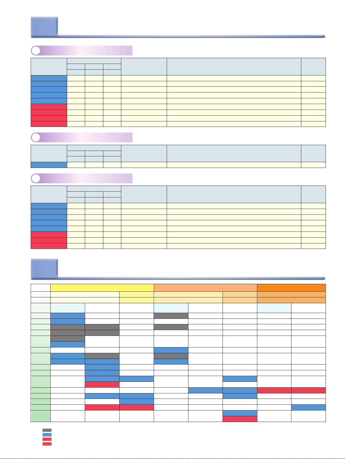
High breakdown capability
1
The product features a glass mesa structure,
the use of which yields a wide forward- and
reverse-biased safe operating area.
Low saturation voltage
2
VCE(sat) = 3 V (max)
Note: Used for 2SC-Series devices without
damper diodes.
Wider range of optimum drive conditions
3
Fluctuation in optimum drive conditions due to variation in device quality has been minimized for
ease of design.
Revised emitter contact shape and optimized chip size
3
Chip design has been optimized using Toshiba simulation technology. The emitter's contact area
has been widened by changing the contact shape below the emitter electrode from comb type to the
new mesh type. As a result, the saturation voltage (V
reduced, thus reducing switching loss.
Features of Fourth and Fifth Generation
Toshiba’s proprietary “glass mesa” structure Contact shape
Glass
Emitter
+
N
P
–
N
+
N
Collector
(sat)) and fall time (tf) have both been
CE
Base
passivation
Conventional comb type
Fourth and fifth-generation
mesh type
4
Page 4
5
Comparison of Product Characteristic Curve, Features and Emitter-Contact Design
Generation
Main application
•
• Features
First Generation
TVs
•
• High-voltage
1500 V
• Improved R-SOA
• Improved switching speeds
fH(max) = 32 kHz
• Development of TO-3P(H)IS
Package
Second Generation
TVs
•
• High-current devices products
Video displays
•
• Improved switching speeds
fH(max) = 64 kHz
• Development of TO-3P(LH)
Package
Design
Emitter contact shape
@
fH, ICP, I
(
t, I
, V
C
B1(end)
)
/ div
CE
, V
@
15.75kHz, 5A, 1A, 1200V
CP
(
200ns, 1A, 10v) / div
Typical Products and Waveforms
TVs Video displays
Comb type I 2SD1556 (1500 V / 6A)
I
C
V
BE
STRIPE type
BE
OA, OV
2SD2253 (1700 V / 6A)
OA, OV
CE
t
Loss
stg
t
stg
Loss
tf Loss
I
C
V
CE
tf Loss
@100kHz, 8A, 1A, 1200V
(
50ns, 1A, 10v) / div
2SC4290A (1500 V / 20A)
I
C
V
CE
OA, OV
t
Loss
stg
tf Loss
Third Generation
TVs
•
• Improvements over
first-generation products
Video displays
•
• Improvements over
second-generation products
• Improved switching speeds
fH(max) = 80 kHz
Fourth Generation
TVs
•
• Improvements over first- and
third-generation products
Digital TVs
•
• Development of new 2000-V
products
Video displays
•
• Improvements over
third-generation products
• Improved switching speeds
fH(max) = 130 kHz
Fifth Generation
Digital TVs
•
• Enhanced 2000-V product line
• Improved speeds for products
incorporating damper diodes
Video displays
•
• Improvements over
fourth-generation products
• Reduced loss
• Improvement in drivability
Comb type II
BE
Mesh type I or
Crystal-mesh type
BE
Mesh type II
BE
2SD2553 (1700 V / 8A)
I
C
V
CE
OA, OV
t
Loss
stg
tf Loss
2SD2638 (1700 V / 7A)
I
C
V
CE
OA, OV
t
Loss
stg
tf Loss
2SC5142 (1500 V / 20A)
I
C
V
CE
OA, OV
t
Loss
stg
tf Loss
2SC5445 (1500 V / 20A)
I
C
V
CE
OA, OV
t
Loss
stg
tf Loss
2SC5695 (1500 V / 22A)
I
C
V
CE
OA, OV
t
Loss
stg
tf Loss
5
Page 5
6
For video displays
1
Product No.
2SC5570
2SC5587
2SC5588
2SC5589
2SC5590
2SC5695
2SC5717
*(S3D20)
*(S3D21)
For color TVs
2
Product No.
2SD2638
For digital TVs
3
Product No.
2SC5570
2SC5588
2SC5590
2SC5612
2SC5716
*(2SC5748)
*(2SC5749)
*(S3D21)
New Products
V
1700
1500
1700
1500
1700
1500
1500
1500
1700
V
1700 28-inch, 15.75 kHz
V
1700
1700
1700
2000
1700
2000
2000
1700
Maximum Ratings
I
CBO
(V)(A)(W)
28
17
15
18
16
22
21
14
28
Maximum Ratings
CBO
(V)(A)(W)
Maximum Ratings
CBO
(V)(A)(W)
28
15
16
22
16
16
28
P
C
220
75
75
200
200
200
75
55
210
I
P
C
750
I
P
C
220
50
50
220
8
55
210
210
210
C
21-inch, 130 kHz
19-inch, 110 kHz
19-inch, 90 kHz
19-inch, 120 kHz
19-inch, 100 kHz
21-inch, 130 kHz
19-inch, 120 kHz
19-inch, 92 kHz
21-inch, 130 kHz
C
C
32-inch, 32 kHz
24-inch, 32 kHz
28-inch, 32 kHz
32-inch, 32 kHz
32-inch, 32 kHz
32-inch, 32 kHz
32-inch, 32 kHz
32-inch, 32 kHz
Target Use Remarks
Device with highest I
High-current version of 2SC5411
1700-V version of 2SC5411
2SC5587 and 2SC5589 use same chip.
2SC5588 and 2SC5590 use same chip.
Equivalent to 2SC5445
2SC5717 and 2SC5695 use same chip.
Equivalent to 2SC5411
Equivalent to 2SC5570
Target Use Remarks
Equivalent to 2SD2553
Target Use Remarks
Device with highest I
˜
1700-V version of 2SC5411
2SC5588 and 2SC5590 use same chip.
˜
˜
= 2000 V series
V
CBO
Built-in damper diode (High-current version of 2SC5143)
= 2000 V series
V
CBO
V
= 2000 V series (built-in damper diode)
CBO
Equivalent to 2SC5570
(max) ratings
C
(max) ratings
C
Note
★
★
★: Production schedules are provisional.
Note
Note
★
★
★
★: Production schedules are provisional.
7
Package
P
C
**
IC (sat)
3 A
3.5 A
4 A
4.5 A
5 A
5.5 A
6 A
7 A
8 A
11 A
12 A
14 A
15 A
17 A
22 A
Notes: **: IC(sat) is value of IC for V
( )
6
*
Product Line Matrix
Built-in
damper diode
2SD2599
2SD2586
2SD2499
S2055N
2SD2539
2SC5339
2SC5280
2SD2559
: 3rd generation (old design)
: 4th generation (new design)
: 5th generation (new design)
: 5th generation (new design under development)
V
CBO
TO-3P(H)IS
40 W to 75 W
No built-in
damper diode
2SD2498
S2000N
2SD2500
2SC5386
2SC5404
2SC5387
2SC5411
*
(S3D20)
2SC5587
2SC5717
= 1500 V V
TO-3P(H)IS
40 W to 75 W
Built-in
2SD2550
2SD2551
2SD2638
2SD2553
2SC5716
CE
(sat).
TO-3P(LH)
180 W to 220 W
No built-in
damper diode
2SC5421
2SC5589
2SC5445
2SC5695
damper diode
= 1700 V V
CBO
No built-in
damper diode
2SC5588
TO-3P(LH)
180 W to 220 W
No built-in
damper diode
2SC5422
2SC5590
2SC5446
2SC5570
*(S3D21)
= 2000 V
CBO
TO-3P(LH)
180 W to 220 W
Built-in
damper diode
No built-in
damper diode
*(2SC5749) *(2SC5748)
2SC5612
Page 6
8
2SC Series
1
Product No.
2SC5280
2SC5339
2SC5386
2SC5387
2SC5404
2SC5411
2SC5421
2SC5422
2SC5445
2SC5446
2SC5570
2SC5587
2SC5588
2SC5589
2SC5590
2SC5612
2SC5695
2SC5716
2SC5717
*(2SC5748)
*(2SC5749)
*(S3D20)
*(S3D21)
Characteristics List
Maximum Ratings
V
CBO
(V)
1500
1500
1500
1500
1500
1500
1500
1700
1500
1700
1700
1500
1700
1500
1700
2000
1500
1700
1500
2000
2000
1500
1700
(A)
10
14
15
15
20
18
28
17
15
18
16
22
22
21
16
16
14
28
I
C
8
7
8
9
8
P
(W)
180
200
200
200
200
200
200
220
200
210
210
210
50
50
50
50
50
60
75
75
55
75
55
C
Built-in
damper
diode
Min Max @5V/I
(–)(
4.0
4.0
4.3
4.3
4.0
4.0
4.0
4.5
4.5
4.0
4.5
5.0
4.8
5.0
4.8
4.8
4.5
3.8
4.5
4.8
4.8
4.0
4.5
8.5
8.0
7.5
7.8
8.0
8.0
8.0
8.5
8.5
8.0
7.5
8.0
8.0
8.0
8.0
9.0
8.5
9.0
8.5
7.5
9.0
8.0
7.5
V
Maxh
5
5
3
3
3
3
3
3
3
3
3
3
3
3
3
3
3
5
3
3
3
3
3
CE(sat)
@ I
11
11
11
15
14
22
14
12
14
12
17
17
17
12
12
11
22
@ I
C
B
1.5
6
1.25
5
1.5
6
8
7
6
2
1.75
2.75
2.75
2.75
3.75
3.5
5.5
3.5
3
3.5
3
4.25
3.75
1.5
3.75
3
3
2.75
5.5
FE
C
)(V)(A)(A)
A
6
5
6
8
7
11
11
11
15
14
22
14
12
14
12
17
17
6
17
12
12
11
22
Switching Time (Max)
t
stg
(µs)(µs)
6.0
6.0
3.5
3.5
3.5
3.5
3.5
3.5
2.2
2.3
1.6
2.0
2.0
2.0
2.0
5.0
2.1
5.0
2.1
5.0
5.0
3.5
1.6
0.50
0.50
0.30
0.30
0.30
0.30
0.30
0.30
0.15
0.15
0.15
0.15
0.15
0.15
0.15
0.35
0.15
0.35
0.15
0.35
0.35
0.30
0.15
t
f
@ fH@ I
(
)(A)(–)
kHz
32
6.0
32
5.0
64
5.0
64
6.0
64
5.5
64
8.5
64
8.5
64
8.0
100
100
130
100
100
100
100
100
100
130
32
32
32
32
90
8.0
7.0
8.0
7.5
6.5
7.5
6.5
8.0
8.0
5.5
8.0
8.0
8.0
6.5
8.0
Gene-
cp
ration
4th
4th
4th
4th
4th
4th
4th
4th
4th
4th
4th
4th
4th
4th
4th
4th
5th
4th
5th
5th
5th
5th
5th
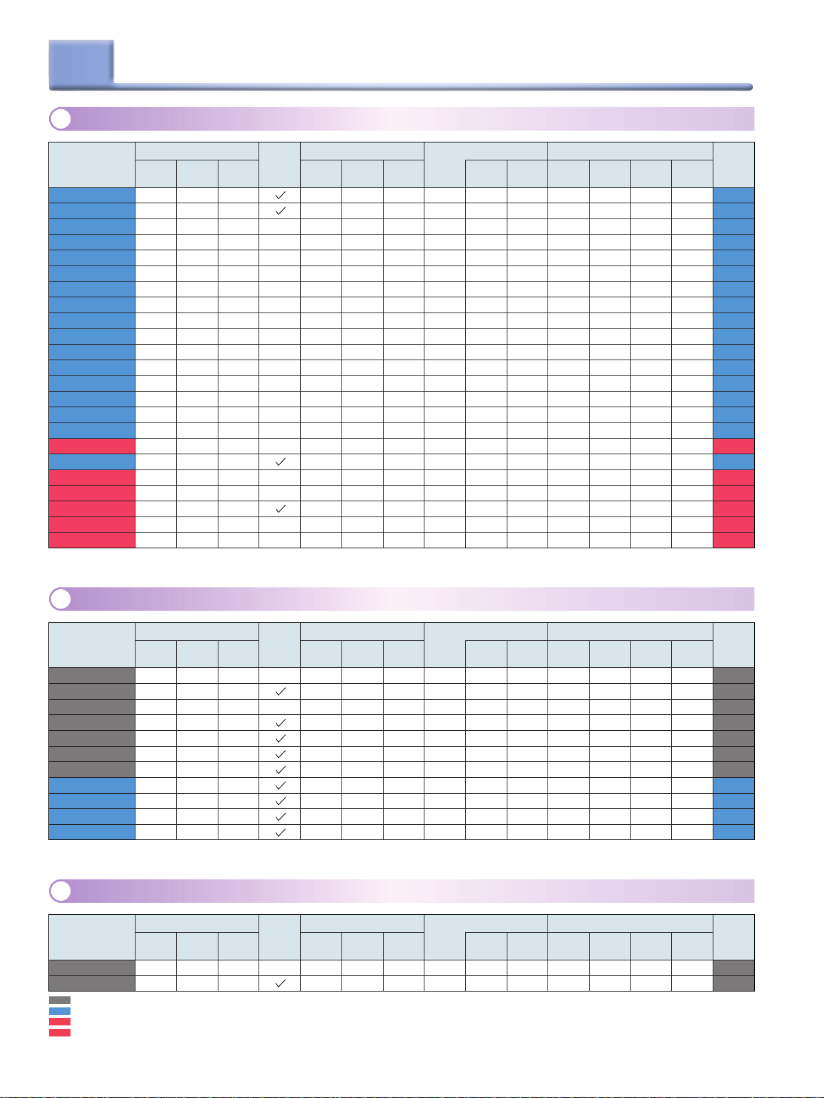
2SD Series
2
Maximum Ratings
Product No.
2SD2498
2SD2499
2SD2500
2SD2539
2SD2550
2SD2551
2SD2553
2SD2559
2SD2586
2SD2599
2SD2638
S2000 / S2055 Series
3
V
CBO
(V)
1500
1500
1500
1500
1700
1700
1700
1500
1500
1500
1700
(A)
3.5
I
10
C
6
6
7
4
5
8
8
5
7
Maximum Ratings
Product No.
S2000N
S2055N
: 3rd generation (old design)
: 4th generation (new design)
: 5th generation (new design)
( )
: 5th generation (new design under development)
*
V
CBO
(V)
1500
1500
(A)
I
C
8
8
P
(W)
50
50
50
50
50
50
50
50
50
40
50
P
(W)
50
50
C
C
Built-in
damper
diode
Built-in
damper
diode
FE
Min Max @5V/I
(–)(
5
5
4
5
8
5
5
5
4.4
8
4.5
Min Max @5V/I
(–)(
4.5
4.5
9
9
8
9
22
10
9
9
8.5
25
7.5
FE
9
9
C
)(V)(A)(A)
A
4
4
6
5
1
4
6
6
3.5
0.5
5.5
C
)(V)(A)(A)
A
4.5
4.5
5
5
3
5
8
5
5
5
5
8
5
5
5
V
CE(sat)
V
CE(sat)
@ I
3.5
5.5
@ I
4.5
4.5
Maxh
@ I
C
B
0.8
4
0.8
4
1.5
6
5
3
4
6
6
3
1
0.8
0.8
1.2
1.2
0.8
0.8
1.2
Maxh
@ I
C
B
1
1
Switching Time (Max)
t
stg
(µs)(µs)
10
11
11
10
10
12
12
10
10
t
f
0.7
0.6
0.7
0.6
9
0.6
1.0
0.7
1.0
0.6
1.0
0.8
9
Switching Time (Max)
t
stg
(µs)(µs)
12
11
0.7
0.6
t
f
@ fH@ I
(
)(A)(–)
kHz
15.75
15.75
15.75
15.75
15.75
15.75
15.75
15.75
15.75
15.75
15.75
@ fH@ I
(
)(A)(–)
kHz
15.75
15.75
3.5
5.5
4.5
4.5
Gene-
cp
ration
3rd
4
3rd
4
3rd
6
3rd
5
3rd
3
3rd
4
3rd
6
4th
6
4th
4th
3
4th
Gene-
cp
ration
3rd
3rd
7
Page 7

9
Application Map
(Reference only)
Generations
2SC Series
1
2SC5411
*(S3D20)
2SC5421
#
2SC5588
#
2SC5590
#
2SC5422
$
*(2SC5748)
¥$
*(2SC5749)
$
2SC5612
2SC5387
2SC5280
¥
2SC5404
2SC5386
¥
2SC5339
¥#
2SC5716
Recommended Peak Collector Current for Actual Use Icp (A)
: (H
: (H
: (LH
: (H
: (LH
: (LH
: (LH
: (H
: (H
: (H
: (H
: (H
: (H
)
)
)
)
)
)
: (LH
: (LH
)
)
)
)
)
)
)
Example
2SDXXXX
2SCXXXX
24
22
20
18
16
)
)
14
12
: 3rd Gen. (old design)
: 4th Gen. (new design)
2SCXXXX
*
(2SCXXXX)
: 5th Gen. (new design)
: under development
Note
DAMPER
¥ : Built-in damper
f
(max) = 32kHz
H
@without additional
Damper diode
V
CBO
CBO
CBO
= 1700V
= 2000V
# : V
$ : V
(Another 1500V)
PACKAGE
(H)
: TO-3P(H)IS
(Full mold type)
(LH)
: T O-3P(LH)
10
#
8
6
4
2
0
0
20 40 60 80 100 120 140
*(S3D21)
#
2SC5570
2SC5717
2SC5445
2SC5695
2SC5587
2SC5589
#
2SC5446
: (LH
: (LH
: (H
: (LH
: (LH
: (H
: (LH
: (LH
)
)
)
)
)
)
)
)
2SD / S2000 / S2055 Series
2
¥
¥#
¥#
¥
¥
¥#
¥
¥
¥#
¥#
2SD2559
2SD2500
2SD2553
2SD2638
2SD2539
S2000N
S2055N
2SD2551
2SD2498
2SD2499
2SD2586
2SD2550
2SD2599
: (H
: (H
: (H
: (H
: (H
: (H
: (H
: (H
: (H
: (H
: (H
: (H
: (H
)
)
)
)
)
)
)
)
)
)
)
)
)
Recommended Peak Collector Current for Actual Use Icp (A)
Horizontal Frequency f
8
(kHz)
H
Note
DAMPER
7
6
5
4
3
¥ : Built-in damper
f
(max) = 32kHz
H
@without additional
Damper diode
V
CBO
CBO
CBO
= 1700V
= 2000V
# : V
$ : V
(Another 1500V)
PACKAGE
(H)
: TO-3P(H)IS
(Full mold type)
(LH)
: T O-3P(LH)
2
1
0
0
20 40 60 80 100 120 140
Horizontal Frequency fH (kHz)
8
Page 8

10
Basic Circuit Structure and Operating Waveform of Horizontal-Deflection Output
Measurement conditions
fH = 69 kHz (duty 50%)
= 5 A
I
CP
= 1200 V
V
CP
Basic circuit structure
I
C
I
Drive
Circuit
SBD
B
VCE(HV-Tr)
(Damper diode)
–V
F
V
BE
HV-Tr
I
E
Damper
diode
Measurement range
X-axis
)
t (time
Y-axis
(
Base-emitter voltage
V
BE
(
Base current
I
B
(
Collector current
I
C
(
–
Reverse emitter current
I
E
(
Forward current
I
F
(
Collector-emitter voltage
V
CE
(
Deflection coil current
I
LY
(
Resonance capacitor current
I
CY
)
)
)
)
)
)
)
I
Cy
I
F
C
L
y
2µs / div
5V / div
2A / div
2A / div
2A / div
2A / div
200V / div
2A / div
)
2A / div
Main operations
Cy
operation
Damper diode
operation
t
s
HV-Tr operation
t
r
Cy
operation
HV-Tr
operation
Damper diode
operation
Operating waveform example
V
OV
I
Ly
y
OA
V
CC
OA
OA
OA
BE
I
B
I
B1(end)
dIB/dt =
I
C
– I
E
IF (Damper diode
I
B1(end)
+ I
B2
t
stg
)
t
stg
I
CP
0.9 x I
0.1 x I
t
I
B2
CP
CP
f
Enlarged wave forms of IB and IC
I
B
OA
I
B1(end)
I
0.9 x I
0.1 x I
t
f
B2
CP
CP
OA
t
stg
I
CP
I
C
OA
OA
OV
I
Cy
I
Ly
(
V
HV-Tr
CE
(
–V
Damper-diode
F
t
s
tr = π Ly Cy
)
)
t
r
V
CP
2µs / div
9
Page 9

11
Test condition
1
·
@ TC = 25˚C
·
f
= 105 kHz (duty 50%, continuous opration)
H
I
= 6.5 A VCP = 953V (Vcc2 = 107 V)
CP
= 8.5 A VCP = 1220V (Vcc2 = 140 V)
I
CP
Test sample
2
Switching Data of 2SC5695
·
·
·
·
·
·
·
·
(Reference only)
–dIB / dt = 4.0A/µs (VCC1 = 24V)
Ly = 63 µH, Cy = 4000 pF
·
·
Mark
= 6.5 A ICP = 8.5 A
I
CP
tstg, tf, –dIB / dt, SW loss –– I
3
2.4
tstg (max) = 1.9 µs
2
1.6
1.2
tstg (µs)tf
0.8
0.4
0.0 0.2 0.4 0.6 0.8 1.0 1.2 1.4 1.6 1.8 2.0
280
240
200
(ns)
160
120
tf (max) = 140 ns
Standerd spec.
·
·
·
·
Test
Sample
tail side
Typ
storage side
B1 (end)
ICP = 6.5 A
ICP = 6.5 A
Best condition area
ICP = 6.5 A
)
h
(1
FE
@5V / 2A @5V / 10A @5V / 17A @17A / 4.25A
)
20 (min
50 (max)8 (min
50.5
33.8
24.1
ICP = 8.5 A
)
hFE (2
)
17 (max)4.8 (min
15.6
12.1
8.2
ICP = 8.5 A
Best condition area
hFE (3
)
8.3 (max
8.2
6.6
4.6
)
)
VCE (sat
3V (max
0.4V
0.6V
2.9V
)
)
10
80
40
0.0 0.2 0.4 0.6 0.8 1.0 1.2 1.4 1.6 1.8 2.0
4.6
4.2
(A/µs)
3.8
/ dt
3.4
B
3.0
–dI
SW loss (W)
0.0 0.2 0.4 0.6 0.8 1.0 1.2 1.4 1.6 1.8 2.0
14
12
10
8
6
4
0.0 0.2 0.4 0.6 0.8 1.0 1.2 1.4 1.6 1.8 2.0
ICP = 6.5 A
SW loss (max) = 11 W
·
·
ICP = 6.5 A
I
B1 (end)
ICP = 8.5 A
ICP = 8.5 A
ICP = 8.5 A
(A)
Page 10

11
Recomended values (rough calculation)
4
Switching Data of 2SC5695
tstg (max)
tf (max)
tstg (max) = (1/fH) x 0.2
tf (max) = (1/fH) x 0.01 + 50ns
Switching loss capacitance (max)
,
@Ta (max) = 40˚C, Tj (max) = 110˚C Recommended
∆Tj (max) = 110˚C –40˚C
∆Tj (max) = 70˚C Recommended
tstg (max) = 1.9µs
tf (max) = 140 ns
thermal resistance
junction to case: Rth (j-c) = 0.625˚C/W (2SC5695)
case to fin (heat-sink): Rth (c-f) = 1˚C/W (supposition)
+) fin (heat-sink) to air: Rth (f-a) = 3.5˚C/W (supposition)
TOTAL (junction on ari): Rth (f-a) = 5.125˚C/W
SW Loss Capasitance (max) = ∆Tj (max)/Rth (j-a) x 80% derating
= 70/5.125 x 0.8
= 10.9
SW loss Capasitance (max) = 11 W
·
·
·
·
·
·
12
Application Circuit Example of 2SC5695
I
C
10 v
0 v
duty 50 %
MOSFET
Semiconductors devices
MOSFET : 2SK2146
SBD : 3GWJ42C
HV-Tr : 2SC5695
Damper diode : 5TUZ52
C
1
R
1
R
3
R
2
Vcc 1 Vcc2
SBD
Others
Vcc1 15 V
Vcc2 47 V (@ 32 kHz)
156 V (@ 100 kHz)
Cy = 4500 pF
Ly = 80 µH
HV-Tr
V
I
B
R
CE
4
Cy Ly L
Damper
diode
1 =
200 Ω
R
2 =
3 Ω
R
3 =
1.85 Ω
R
4 =
15 Ω
R
1 =
200 pF
C
2 =
3.3 µF
C
=
10 mH
L
C
2
Operating waveform example (21-inch ultra-high-resolution monitor) fH = 32 kHz to 100 kHz monitor
: 0
: 0
100 ns / div
I
C
I
B
V
CE
X-axis
Y-axis
@ fH = 32 kHz
Icp = 9 A
I
dI
·
B1
(end) = 0.75 A
·
·
B
/ dt = 3.5 A / µs
·
500 ns / div
: 1 A / div VCE : 200 V / div
I
B
IC : 1 A / div
IB: 0
I
I
B
IC: 0
V
V
: 0
CE
CE
IB : 1 A / div VCE : 10 V / div
IC : 1 A / div
C
I
B
IC: 0
V
CE
@ fH = 100 kHz
Icp = 8 A
·
B1
(end) = 1. 1 A
I
·
·
B
/ dt = 3.8 A / µs
dI
·
V
I
B
IC: 0
CE
: 0
: 0
500 ns / div
I
C
I
B
V
CE
500 ns / div
V
I
B
IC: 0
CE
: 0
: 0
100 ns / div
I
C
I
B
V
CE
100 ns / div
11
Page 11

13
5.45
123
5.45
1. Base
2. Collector
3. Emitter
4.95 ± 0.5 4.45 ± 0.5
9.4 ± 0.5
7.0 ± 0.5
1.8
(8.5)
(8)
5.45
123
5.45
1. Base
2. Collector
3. Emitter
15 ± 1
6.5 ± 0.5
5.3 ± 0.5
1.25
Lead-Forming
TO-3P(H)IS
2-16E302A 2-16E303A
(2.25)(2.75)
10.2±0.6
15.2±0.8
5.45
5.45
4.0 4.0
8.0
1. Base
123
2. Collector
3. Emitter
2-16E305A 2-16E306A
1.25
13.0 ± 0.5
5.45
123
5.45
5.3 ± 0.5
1. Base
2. Collector
3. Emitter
5.45
5.45
123
5.6 ± 0.5
6.9 ± 0.5
1. Base
2. Collector
3. Emitter
(Unit : mm)
2.5
7.0 ± 0.5
6.5 ± 0.5
12
2-16E307A 2-16E309A
15.4 ± 0.5
5.45
123
5.45
1. Base
2. Collector
3. Emitter
2-16E311A 2-16E313A
1.25
6.5 ± 0.56.55 min
15.4 ± 0.5
5.45
5.45
5.3 ± 0.5
5.45
(10.5)
4.95 ± 0.5 4.45 ± 0.5
5.45
1. Base
2. Collector
123
3. Emitter
123
9.4 ± 0.5
1. Base
2. Collector
3. Emitter
2.2
3.3 ± 0.5
(11)
Page 12

13
TO-3P(H)IS
2-16E314A 2-16E315A
2.0
7.0 ± 0.5
35.4 ± 1.0
5.45
4.95 ± 0.5 4.45 ± 0.5
5.45
9.4 ± 0.5
5.45
123
1. Base
2. Collector
123
3. Emitter
2-16E316A
5.85 ± 0.5
10.35 ± 0.5
0.82 ± 0.5
4.0 ± 0.5
1. Base
2. Collector
3. Emitter
5.45
123
1.0.5 ± 0.5 2.95 ± 0.5
5.45
5.45
4 ± 0.5
8.0 ± 0.5
2.25
+ 1.0
4 ± 0.5
1. Base
2. Collector
3. Emitter
2.75
0.5
–
10.2
(Unit : mm)
TO-3P(LH)
5.45 ± 0.15 5.45 ± 0.15 5.45 ± 0.6
2-21F208A 2-21F218A
3.0
6.5 ± 0.6
17.0 ± 0.8
20.0 ± 0.6
5.45 ± 0.15 5.45 ± 0.15
2
1. Base
123
2. Collector (heat sink)
3. Emittor
1
3
3.5 ± 0.5
7.0 ± 0.8
18.5 ± 0.8
4.0 ± 0.54.0 ± 0.5
8.0 ± 1.0
1. Base
2. Collector (heat sink)
3. Emitter
(Unit : mm)
13
Page 13

14
Explanation of markings
Toshiba hor izontal-deflection output transistors are manufactured in Japan (at the Himeji Semiconductor Works)
and in Malaysia (at Toshiba Electronics Malaysia Sdn. Bhd.). Toshiba Electronics Malaysia Sdn. Bhd. only
manufactures T O-3P(H)IS products.
Markings
(As of April 2001)
Place of Manufacture
Package type
Marking Example
Definition
TOSHIBA ELECTRONICS
MALAYSIA SDN. BHD
(made in Malaysia)
TO-3P(H)IS TO-3P(LH)
TOSHIBA
C5411
21A
3
*
Himeji Semiconductor Works
(made in Japan)
1
*
2
*
3
*
4
*
5
TOSHIBA
2SC5570
1A2
JAPAN
1
*
2
*
4
*
*
1: Manufacturer’s marking: “T”, “ ”, “TOSHIBA”
*
2: Product number or abbreviated product number
*
3: Code: “1”, “2”, “3”, “A”, “B”, “C”
*
4: Lot number: month and year of manufacture
*
Month of manufacture: January to December are denoted by the letters A to L respectively.
Year of manufacture: last decimal digit of year of manufacture
“1A”, as shown on the above package, indicates manufacture in January 2001.
5: Country of origin
*
Since TO-3P(LH) packages are only made in Japan, “JAP AN” is displayed.
14
15
Sample label
Package Label
(As of April 2001)
P/N:
TYPE
ADDC Q,TY PCS.
NOTE
BARCORD
MADE IN JAPAN
Page 14

16
Package Specifications
(As of April 2001)
Package type
Packing Type
Tray
Dimensions
(unit: mm)
TO-3P(H)IS TO-3P(LH)
100 per tray, 5 trays per carton
Tolerance: ±0.7
Material: rigid vinyl chloride
184
61
76
67.6
19
14
28
6
8
290
16
12.4
Tolerance: ±0.7
Material: rigid vinyl chloride
19
27 21
290
184
52
72.5
24
Carton
Dimensions
(unit: mm)
Label
85
190
305
Label
116
303
190
15
Page 15

17
2SC Series
1
Product
No.
2SC3715
2SC3716
2SC3884A
2SC3885A
2SC3886A
2SC3887
2SC3887A
2SC3888
2SC3888A
2SC3889
2SC3889A
2SC3892
2SC3892A
2SC3893
2SC3893A
2SC4288
2SC4288A
2SC4289
2SC4289A
2SC4290
2SC4290A
2SC4531
2SC4532
2SC4542
2SC4560
2SC4608
2SC4757
2SC4758
2SC4759
2SC4760
2SC4761
2SC4762
2SC4763
2SC4764
2SC4765
2SC4766
2SC4806
2SC4830
2SC4916
2SC5048
2SC5129
2SC5142
2SC5143
2SC5144
2SC5148
2SC5149
2SC5150
2SC5331
2SC5332
1
( * )
2
3
4
5
6
List of Superseded, Final-Phase and Discontinued Products
Superseded
Products
Electrical characteristics and packages are same.
Electrical characteristics have are high grade.
Electrical characteristics are low grade.
Package (allowable power disspation) are high grade.
Package (allowable power disspation) are low grade.
Damper diode is built-in or not.
Final
Phase
Products
Discontinued
Products
Maximum Ratings
CBO
(V)
I
(A)
12
12
16
16
20
20
10
10
10
10
10
12
10
20
10
20
12
10
15
14
C
4
5
6
7
8
6
6
7
7
8
8
7
7
8
8
200
200
200
200
200
200
200
8
200
7
8
8
200
6
7
8
6
5
6
5
6
7
200
200
8
180
200
V
1500
1500
1500
1500
1500
1400
1500
1400
1500
1400
1500
1400
1500
1400
1500
1400
1500
1400
1500
1400
1500
1500
1700
1500
1500
1700
1500
1500
1500
2000
1700
1500
1500
1500
1700
1700
1700
1500
1500
1500
1500
1500
1700
1700
1500
1500
1700
1500
1700
P
(W)
50
50
50
50
50
80
80
80
80
80
80
50
50
50
50
50
50
80
50
50
50
50
50
50
50
50
50
50
50
50
50
50
50
50
50
50
C
Built-in
damper
diode
Max
Notes: : 1st generation
: 2nd generation (final-phase or discontinued products)
: 3rd generation (old design superseded products)
: 4th generation (new design)
5
5
5
5
5
5
5
5
5
5
5
5
5
5
5
5
5
5
5
5
5
5
5
5
5
5
5
5
5
5
5
5
5
5
5
5
5
5
5
3
3
3
3
3
3
5
3
3
3
CE(sat)
@ I
(A)
2.5
10
10
12
12
14
14
4.5
3.5
4.5
3.5
14
11
(As of April 2001)
(V)
@ I
C
(A)
0.6
3
0.8
4
5
1.2
6
1.5
4
4
5
1.2
5
1.2
6
1.5
6
1.5
5
1.2
5
1.2
6
1.5
6
1.5
2.5
2.5
3.5
3.5
7
1.7
8
7
1.7
7
1.7
6
1.5
1.2
5
1.5
6
1.7
7
1.5
6
1.3
5
1.2
6
0.8
4
1.3
4
5
8
6
1.5
3.5
6
1.5
2.75
8
5
1.3
6
1.5
9
2.25
8
B
1
1
1
3
3
2
1
1
1
1
1
2
2
2
Package TypeV
(H)IS(
BS)(LH
)
TO-3
*
Recommended
Replacement
and Remarks
2SD2599;
2SD2599;
2SC5386;
2SC5386;
2SC5386;
2SC5386;
2SC5386;
2SC5386;
2SC5386;
2SC5386;
2SC5386;
2SC5339;
2SC5339;
2SC5280;
2SC5280;
2SC5421;
2SC5421;
2SC5589;
2SC5589;
2SC5589;
2SC5589;
2SC5280;
2SC5422;
2SC5404;
2SC5404;
2SC5422;
2SC5386;
2SC5386;
2SC5404;
2SC5612;
2SC5588;
2SC5280;
2SC5280;
2SC5339;
2SC5716;
2SC5716;
2SC5588;
2SC5386;
2SC5280;
2SC5387;
2SC5386;
2SC5589;
2SC5716;
2SC5590;
2SC5386;
2SC5339;
2SC5588;
2SC5421;
2SC5422;
2
1
2
2
2
2
5
2
5
2
5
2
5
5
5
1
1
1
1
5
5
2
2
2
2
3
2
1
5
2
2
1
1
2
2
1
3
2
2
2
2
2
1
1
1
1
3
1
2
1
2
2
2
16
Page 16

17
2SD Series
2
Product
No.
2SD811
2SD818
2SD819
2SD820
2SD821
2SD822
2SD868
2SD869
2SD870
2SD871
2SD1279
2SD1425
2SD1426
2SD1427
2SD1428
2SD1429
2SD1430
2SD1431
2SD1432
2SD1433
2SD1543
2SD1544
2SD1545
2SD1546
2SD1547
2SD1548
2SD1553
2SD1554
2SD1555
2SD1556
2SD2089
2SD2095
2SD2125
2SD2253
2SD2348
2SD2349
2SD2428
2SD2454
Superseded
Products
Final
Phase
Products
Discontinued
Products
Maximum Ratings
CBO
(V)
900
I
(A)
2.5
3.5
2.5
3.5
10
2.5
3.5
2.5
3.5
2.5
3.5
2.5
3.5
3.5
10
C
6
5
6
7
5
6
5
6
5
6
7
5
6
7
8
5
6
5
6
6
8
8
7
V
1500
1500
1500
1500
1500
1500
1400
1500
1500
1400
1500
1500
1500
1500
1500
1500
1500
1500
1500
1500
1500
1500
1500
1500
1500
1500
1500
1500
1500
1500
1500
1500
1700
1500
1500
1700
1700
P
(W)
50
50
50
50
50
50
50
50
50
50
50
80
80
80
80
80
80
80
80
80
40
40
50
50
50
50
40
40
50
50
40
50
50
50
50
50
200
50
C
Built-in
damper
diode
Max
10
8
8
5
5
5
8
8
5
5
5
8
8
5
5
8
8
5
5
5
8
8
5
5
5
5
8
8
5
5
1
5
5
5
5
5
5
5
CE(sat)
@ I
(A)
2.5
2.2
3.5
(V)
@ I
C
(A)
0.25
2
0.6
3
0.8
4
0.8
5
6
1.2
2
0.6
3
0.8
4
0.8
5
8
2
0.6
3
0.8
4
0.8
5
2
0.6
3
0.8
4
0.8
5
6
1.2
2
0.6
3
0.8
4
0.8
5
6
1.2
8
2
0.6
3
0.8
4
0.8
5
0.7
0.8
5
5
6
1.2
7
1.4
6
1.2
6
1.2
B
1
1
2
1
1
1
2
1
1
1
(H)IS(
Package TypeV
BS)(LH
*
Recommended
TO-3
Replacement
and Remarks
2SC3657;
2SD2599;
2SD2599;
2SC5386;
2SC5386;
2SC5386;
2SD2599;
2SD2599;
2SD2499;
2SD2539;
2SC5404;
2SD2599;
2SD2599;
2SD2499;
2SD2539;
2SD2498;
2SD2498;
2SD2498;
2SC5386;
2SC5404;
2SD2498;
2SD2498;
2SD2498;
2SC5386;
2SC5404;
2SC5404;
2SD2599;
2SD2599;
2SD2499;
2SD2539;
2SD2599;
2SD2586;
2SD2539;
2SD2638;
2SC5280;
2SC5280;
2SD2553;
2SD2638;
5
6
6
2
2
2
2
5
5
1
1
1
2
5
5
1
5
5
5
5
5
5
2
2
1
1
1
1
2
1
1
1
1
1
1
1
3
3
5
1
)
S2000 / S2055 Series
3
Product
No.
Superseded
Products
S2000
S2000A
S2000AF
S2000F
S2055
S2055A
S2055AF
S2055F
Electrical characteristics and packages are same.
1
( * )
Electrical characteristics have are high grade.
2
Electrical characteristics are low grade.
3
Package (allowable power disspation) are high grade.
4
Package (allowable power disspation) are low grade.
5
Damper diode is built-in or not.
6
Final
Phase
Products
Discontinued
Products
Maximum Ratings
CBO
(V)
I
(A)
C
5
5
5
5
5
5
5
5
V
1500
1500
1500
1500
1500
1400
1500
1500
P
(W)
80
80
50
50
80
80
50
50
C
(V)
)
Built-in
damper
diode
CE(sat
@ I
@ I
Max
Notes: : 1st generation
: 2nd generation (final-phase or discontinued products)
: 3rd generation (old design)
: 4th generation (new design)
C
(A)
(A)
5
1
1
5
5
1
1
5
4.5
4.5
4.5
4.5
4.5
4.5
4.5
4.5
2
2
2
2
2
2
2
2
B
(H)IS(
Package TypeV
BS)(LH
)
TO-3
*
Recommended
Replacement
and Remarks
S2000N;
S2000N;
S2000N;
S2000N;
S2055N;
S2055N;
S2055N;
S2055N;
5
2
5
1
2
2
5
5
1
2
17
Page 17

18 18
Table of Replacement
Package
P
max
C
**IC(sat)
2 A
2.2 A
2.5 A
3 A
3.5 A
4 A
4.5 A
5 A
Built-in
damper diode
2SD1553
2SD2089
2SC3715
2SC3716
2SD1554
2SD2599
2SD2095
2SD2586
2SC4764
2SD1555
2SD2499
S2055AF
S2055F
S2055N
2SC4762
2SC4916
2SC5149
2SC5339
2SD1556
2SD2125
2SD2539
TO-3P(H)IS
40 W to 75 W
(8V)
(
(
(
(
(
(
(
(
(
(
(
(
(
(
(
(
(
(
(
(
5.5 A
6 A
7 A
2SC4763
2SC5280
2SD2348
2SD2559
2SC4531
2SC2349
(
(
(
(
(
(
8 A
9 A
10 A
11 A
12 A
14 A
15 A
17 A
22 A
Notes: **: IC (sat) is value of IC for V
: Superseded, final-phase or discontinued products
: 3rd generation (old design)
: 4th generation (new design)
1V
5V
5V
8V
8V
5V
5V
5V
5V
5V
1V
5V
5V
5V
5V
5V
5V
5V
5V
5V
5V
5V
5V
5V
5V
5V
CE
)
)
)
)
)
)
)
)
)
)
)
)
)
)
)
)
)
)
)
)
)
)
)
)
)
)
(sat).
No built-in
damper diode
2SD1543
2SD1544
2SC3844A
2SC4830
2SD1545
2SD2498
S2000AF
S2000F
S2000N
2SC3885A
2SC4757
2SC5148
2SD1546
2SC3886A
2SC4758
2SC5129
2SC5386
2SD1547
2SD2500
2SC4542
2SC4759
2SC5404
2SD1548
2SC5048
2SC5387
2SC5411
*(S3D20
2SC5587
2SC5717
)
(8V)
(
)
8V
)
(
5V
(
)
5V
(
)
5V
(
)
5V
(
)
1V
(
)
5V
)
(
5V
(
)
5V
(
)
5V
)
(
3V
(
)
5V
(
)
5V
(
)
5V
(
)
3V
(
)
3V
(
)
5V
(
)
3V
(
)
5V
)
(
5V
(
)
3V
(
)
5V
(
)
3V
(
)
3V
(
)
3V
(
)
3V
)
(
3V
(5V) means V
( )
*
V
Built-in
damper diode
2SD868
2SD869
2SD870
2SD871
CE
: 5th generation (new design)
: 5th generation (new design under development)
= $900V, *1400V,1500 V V
CBO
TO-3 TO-3P(BS
50 W
Built-in
damper diode
2SD1425
2SD1426
(8V)
(
8V
(8V)
(
8V
)
No built-in
damper diode
2SD818
$2SD811
2SD819
(
10V
(8V)
(
8V
)
)
)
80 W
No built-in
damper diode
2SD1429
)
2SD1430
180 W to 220 W
damper diode
(8V)
(
)
8V
TO-3P(LH
No built-in
)
Built-in
dampe dioder
2SD2550
2SC4765
)
(
2SD820
5V
(
)
5V
2SD821
(
5V
(
5V
)
2SD1427
S2055
S2055A
)
*2SC3892
2SC3892A
2SD1429
(
5V
(
5V
(
1V
(
5V
(
5V
(
5V
)
*2SC3887
2SC3887A
2SD1431
)
S2000
)
S2000A
)
*2SC3888
)
2SC3888A
)
2SD1432
)
(
5V
(
)
5V
(
)
5V
(
)
5V
(
)
1V
(
)
5V
(
)
5V
)
(
5V
2SD2551
2SC4766
2SD2253
2SD2638
2SD822
5V
)
*2SC3893
2SC3893A
(
5V
(
5V
)
*2SC3889
)
2SC3889A
2SD1433
)
(
5V
(
)
5V
(
)
5V
2SC5143
2SC5716
2SD2428
(
2SD2454
2SD2553
(
)
5V
*2SD1279
2SC4560
(
)
5V
2SC5331
*2SC4288
2SC4288A
2SC5421
*2SC4289
2SC4289A
*2SC4290
2SC4290A
2SC5142
2SC5589
2SC5445
2SC5695
(sat) = 5 V
(5V)
(
5V
(
3V
(
5V
(
5V
(
5V
(
5V
(
3V
(
3V
(
3V
(
3V
)
)
)
)
)
)
)
)
)
)
= 1700 V V
CBO
TO-3P(H)IS TO-3P(LH
40 W to 75 W
No built-in
damper diode
(5V)
(
)
5V
2SC4806
(
)
5V
)
(
2SC4761
5V
(
)
5V
)
(
5V
(
)
2SC5150
3V
(
)
5V
(
)
5V
(
)
5V
(
)
5V
2SC4532
2SC5588
180 W to 220 W 180 W to 220 W
No built-in
damper diode
(5V)
)
(
5V
(
)
3V
2SC4608
(
)
5V
2SC5332
2SC5422
(
)
3V
2SC5590
2SC5446
2SC5570
*(S3D21
)
)
(5V)
(
3V
(
3V
(
3V
(
3V
(
3V
damper diode
)
)
)
*(2SC5749
)
)
Built-in
CBO
TO-3P(LH
)
= 2000 V
)
No built-in
damper diode
2SC4760
*(2SC5748
2SC5612
Package
P
max
C
**IC(sat)
2 A
2.2 A
2.5 A
3 A
3.5 A
4 A
4.5 A
5 A
5.5 A
(5V)
)
(3V)
6 A
7 A
8 A
9 A
10 A
11 A
12 A
14 A
15 A
17 A
22 A
18 19
Page 18

OVERSEAS SUBSIDIARIES AND AFFILIATES
Toshiba America
Electronic Components, Inc.
Headquarters-Irvine, CA
9775 Toledo Way, Irvine, CA 92618, U.S.A.
Tel: (949)455-2000 Fax: (949)859-3963
Boulder, CO
3100 Arapahoe Avenue, Ste. 500,
Boulder, CO 80303, U.S.A.
Tel: (303)442-3801 Fax: (303)442-7216
Boynton Beach, FL(Orlando)
11924 W. Forest Hill Blvd., Ste. 22-337,
Boynton Beach, FL 33414, U.S.A.
Tel: (561)374-6193 Fax: (561)374-6194
Deerfield, IL(Chicago)
One Pkwy., North, Suite 500, Deerfield,
IL 60015-2547, U.S.A.
Tel: (847)945-1500 Fax: (847)945-1044
Duluth, GA(Atlanta)
3700 Crestwood Parkway, Ste. 460,
Duluth, GA 30096, U.S.A.
Tel: (770)931-3363 Fax: (770)931-7602
Edison, NJ
2035 Lincoln Hwy. Ste. #3000, Edison
NJ 08817, U.S.A.
Tel: (732)248-8070 Fax: (732)248-8030
Orange County, CA
2 Venture Plaza, #500 Irvine, CA 92618, U.S.A.
Tel: (949)453-0224 Fax: (949)453-0125
Portland, OR
1700 NW 167th Place, #240,
Beaverton, OR 97006, U.S.A.
Tel: (503)629-0818 Fax: (503)629-0827
Raleigh, NC
5511 Capitol Center Dr., #114,
Raleigh, NC 27606, U.S.A.
Tel: (919)859-2800 Fax: (919)859-2898
Richardson, TX(Dallas)
777 East Campbell Rd., Suite 650, Richardson,
TX 75081, U.S.A.
Tel: (972)480-0470 Fax: (972)235-4114
San Jose Engineering Center, CA
1060 Rincon Circle, San Jose, CA 95131, U.S.A.
Tel: (408)526-2400 Fax:(408)526-2410
Wakefield, MA(Boston)
401 Edgewater Place, Suite #360, Wakefield,
MA 01880-6229, U.S.A.
Tel: (781)224-0074 Fax: (781)224-1095
Toshiba Do Brasil S.A.
Electronic Components Div.
Estrada Dos Alvarengas, 5. 500-Bairro Alvarenga
09850-550-Sao Bernardo do campo - SP
Tel: (011)7689-7171 Fax: (011)7689-7189
The information contained herein is subject to change without notice.
The information contained herein is presented only as a guide for the applications of our products.
No responsibility is assumed by TOSHIBA for any infringements of patents or other rights of the third parties which may result
from its use. No license is granted by implication or otherwise under any patent or patent rights of TOSHIBA or others.
TOSHIBA is continually working to improve the quality and reliability of its products. Nevertheless, semiconductor devices in
general can malfunction or fail due to their inherent electrical sensitivity and vulnerability to physical stress. It is the
responsibility of the buyer, when utilizing TOSHIBA products, to comply with the standards of safety in making a safe design for
the entire system, and to avoid situations in which a malfunction or failure of such TOSHIBA products could cause loss of
human life, bodily injury or damage to property. In developing your designs, please ensure that TOSHIBA products are used
within specified operating ranges as set forth in the most recent TOSHIBA products specifications. Also, please keep in mind
the precautions and conditions set forth in the "Handling Guide for Semiconductor Devices," or "TOSHIBA Semiconductor
Reliability Handbook" etc..
The Toshiba products listed in this document are intended for usage in general electronics applications (computer, personal
equipment, office equipment, measuring equipment, industrial robotics, domestic appliances, etc.).
These Toshiba products are neither intended nor warranted for usage in equipment that requires extraordinarily high quality and/or
reliability or a malfunction or failure of which may cause loss of human life or bodily injury ("Unintended Usage"). Unintended Usage
include atomic energy control instruments, airplane or spaceship instruments, transportation instruments, traffic signal instruments,
combustion control instruments, medical instruments, all types of safety devices, etc.. Unintended Usage of Toshiba products listed
in this document shall be made at the customer’s own risk.
Toshiba Electronics Europe GmbH
Düsseldorf Head Office
Hansaallee 181, D-40549 Düsseldorf
Germany
Tel: (0211)5296-0 Fax: (0211)5296-400
München Office
Büro München Hofmannstrasse 52,
D-81378, München, Germany
Tel: (089)748595-0 Fax: (089)748595-42
Toshiba Electronics France SARL
Immeuble Robert Schumann 3 Rue de Rome,
F-93561, Rosny-Sous-Bois, Cedex, France
Tel: (1)48-12-48-12 Fax: (1)48-94-51-15
Toshiba Electronics Italiana S.R.L.
Centro Direzionale Colleoni
Palazzo Perseo Ingr. 2-Piano 6,
Via Paracelso n.12,
1-20041 Agrate Brianza Milan, Italy
Tel: (039)68701 Fax:(039)6870205
Toshiba Electronics España, S.A.
Parque Empresarial San Fernando Edificio Europa,
1a Planta, ES-28831 Madrid, Spain
Tel: (91)660-6700 Fax:(91)660-6799
Toshiba Electronics(UK) Limited
Riverside Way, Camberley Surrey,
GU15 3YA, U.K.
Tel: (01276)69-4600 Fax: (01276)69-4800
Toshiba Electronics Scandinavia AB
Gustavslundsvägen 12, 2nd Floor
S-161 15 Bromma, Sweden
Tel: (08)704-0900 Fax: (08)80-8459
Toshiba Electronics Asia
(Singapore) Pte. Ltd.
Singapore Head Office
438B Alexandra Road, #06-08/12 Alexandra
Technopark, Singapore 119968
Tel: (278)5252 Fax: (271)5155
Bangkok Office
135 Moo 5 Bangkadi Industrial Park, Tivanon Rd.,
Bangkadi Amphur Muang Pathumthani, Bangkok, 12000,
Thailand
Tel: (02)501-1635 Fax: (02)501-1638
Toshiba Electronics Trading
(Malaysia)Sdn. Bhd.
Kuala Lumpur Head Office
Suite W1203, Wisma Consplant, No.2,
Jalan SS 16/4, Subang Jaya, 47500 Petaling Jaya,
Selangor Darul Ehsan, Malaysia
Tel: (3)731-6311 Fax: (3)731-6307
Penang Office
Suite 13-1, 13th Floor, Menard Penang Garden,
42-A, Jalan Sultan Ahmad Shah,
100 50 Penang, Malaysia
Tel: 4-226-8523 Fax: 4-226-8515
Toshiba Electronics Philippines, Inc.
26th Floor, Citibank Tower, Valero Street, Makati,
Manila, Philippines
Tel: (02)750-5510 Fax: (02)750-5511
010124 (D)
Toshiba Electronics Asia, Ltd.
Hong Kong Head Office
Level 11, Top Glory Insurance Building, Grand Century
Place, No.193, Prince Edward Road West,
Mong Kok, Kowloon, Hong Kong
Tel: 2375-6111 Fax: 2375-0969
Beijing Office
Rm 714, Beijing Fortune Building,
No.5 Dong San Huan Bei-Lu, Chao Yang District,
Beijing, 100004, China
Tel: (010)6590-8795 Fax: (010)6590-8791
Chengdu Office
Unit F, 18th Floor, New Times Plaza, 42 Wenwu Road,
Xinhua Avenue, Chengdu, 610017, China
Tel: (028)675-1773 Fax: (028)675-1065
Shenzhen Office
Rm 3010-3012, Office Tower Shun Hing Square,
Di Wang Commercial Centre, 333 ShenNan
East Road, Shenzhen, 518008, China
Tel: (0755)246-1582 Fax: (0755)246-1581
Toshiba Electronics Korea Corporation
Seoul Head Office
14/F, KEC B/D, 257-7 Yangjae-Dong,
Seocho-ku, Seoul, Korea
Tel: (02)589-4334 Fax: (02)589-4302
Gumi Office
6/F, Ssangyong Investment Securities B/D,
56 Songjung-Dong, Gumi City
Kyeongbuk, Korea
Tel: (82)54-456-7613 Fax: (82)54-456-7617
Toshiba Technology Development
(Shanghai) Co., Ltd.
23F, Shanghai Senmao International Building, 101
Yin Cheng East Road, Pudong New Area, Shanghai,
200120, China
Tel: (021)6841-0666 Fax: (021)6841-5002
Tsurong Xiamen Xiangyu Trading
Co., Ltd.
8N, Xiamen SEZ Bonded Goods Market Building,
Xiamen, Fujian, 361006, China
Tel: (0592)562-3798 Fax: (0592)562-3799
Toshiba Electronics Taiwan
Corporation
Taipei Head Office
17F, Union Enterprise Plaza Bldg. 109
Min Sheng East Rd., Section 3, 0446 Taipei,
Taiwan
Tel: (02)514-9988 Fax: (02)514-7892
Kaohsiung Office
16F-A, Chung-Cheng Bldg., Chung-Cheng 3Rd.,
80027, Kaohsiung, Taiwan
Tel: (07)222-0826 Fax: (07)223-0046
Electronic Devices Sales & Marketing Division
1-1, Shibaura 1-chome, Minato-ku, Tokyo, 105-8001, Japan
Tel: +81-3-3457-3405 Fax: +81-3-5444-9431
Website: http://doc.semicon.toshiba.co.jp/indexus.htm
©2001 TOSHIBA CORPORATION
Printed in Japan
 Loading...