

Toshiba D-VR60DTKF Service Manual
SERVICE MANUAL
TOSHIBA CORPORATION 2008
The above model is classified as a green product (*1), as indicated by the underlined serial
number. This Service Manual describes replacement parts for the green product. When
repairing this green product, use the part(s) described in this manual and lead-free solder (*2).
For (*1) and (*2), see the next page.
FILE NO. 810-200810GR
DVD Video Recorder
/Video Cassette Recorder
D-VR60DTKF
Published in Japan, Apr. 2008 GREEN
SECAMPAL
ON/STANDBY
VCR
REC
DUBBING
PROGRAM
VCR/DVD
REC
DVD
DVDVCR
PAL SECAM

(*1) GREEN PRODUCT PROCUREMENT
The EC is actively promoting the WEEE & RoHS Directives that define standards for recycling
and reuse of Waste Electrical and Electronic Equipment and for the Restriction of the use of
certain Hazardous Substances. From July 1, 2006, the RoHS Directive will prohibit any
marketing of new products containing the restricted substances.
Increasing attention is given to issues related to the global environmental. Toshiba Corporation
recognizes environmental protection as a key management tasks, and is doing its utmost to
enhance and improve the quality and scope of its environmental activities. In line with this,
Toshiba proactively promotes Green Procurement, and seeks to purchase and use products,
parts and materials that have low environmental impacts.
Green procurement of parts is not only confined to manufacture. The same green parts used in
manufacture must also be used as replacement parts.
(*2) LEAD-FREE SOLDER
This product is manufactured using lead-free solder as a part of a movement within the consumer
products industry at large to be environmentally responsible. Lead-free solder must be used in the
servicing and repair of this product.
WARNING
This product is manufactured using lead free solder.
DO NOT USE LEAD BASED SOLDER TO REPAIR THIS PRODUCT !
The melting temperature of lead-free solder is higher than that of leaded solder by 86°F to 104°F
(30°C to 40°C). Use of a soldering iron designed for lead-based solders to repair product made
with lead-free solder may result in damage to the component and or BOARD being soldered.
Great care should be made to ensure high-quality soldering when servicing this product —
especially when soldering large components, through-hole pins, and on BOARDs — as the level
of heat required to melt lead-free solder is high.

MAIN SECTION
DVD VIDEO RECORDER /
VIDEO CASSETTE RECORDER
D-VR60DTKF
TABLE OF CONTENTS
Specifications . . . . . . . . . . . . . . . . . . . . . . . . . . . . . . . . . . . . . . . . . . . . . . . . . . . . . . . . . . . . . . . . . . . . . . . . . . 1-1-1
Laser Beam Safety Precautions. . . . . . . . . . . . . . . . . . . . . . . . . . . . . . . . . . . . . . . . . . . . . . . . . . . . . . . . . . . . 1-2-1
Important Safety Precautions. . . . . . . . . . . . . . . . . . . . . . . . . . . . . . . . . . . . . . . . . . . . . . . . . . . . . . . . . . . . . . 1-3-1
Standard Notes for Servicing . . . . . . . . . . . . . . . . . . . . . . . . . . . . . . . . . . . . . . . . . . . . . . . . . . . . . . . . . . . . . . 1-4-1
Preparation for Servicing . . . . . . . . . . . . . . . . . . . . . . . . . . . . . . . . . . . . . . . . . . . . . . . . . . . . . . . . . . . . . . . . . 1-5-1
Cabinet Disassembly Instructions . . . . . . . . . . . . . . . . . . . . . . . . . . . . . . . . . . . . . . . . . . . . . . . . . . . . . . . . . . 1-6-1
Electrical Adjustment Instructions . . . . . . . . . . . . . . . . . . . . . . . . . . . . . . . . . . . . . . . . . . . . . . . . . . . . . . . . . . 1-7-1
How to Initialize the DVD Recorder & VCR . . . . . . . . . . . . . . . . . . . . . . . . . . . . . . . . . . . . . . . . . . . . . . . . . . . 1-8-1
Firmware Renewal Mode . . . . . . . . . . . . . . . . . . . . . . . . . . . . . . . . . . . . . . . . . . . . . . . . . . . . . . . . . . . . . . . . . 1-9-1
Remote Control Key Code . . . . . . . . . . . . . . . . . . . . . . . . . . . . . . . . . . . . . . . . . . . . . . . . . . . . . . . . . . . . . . . . 1-9-2
Troubleshooting . . . . . . . . . . . . . . . . . . . . . . . . . . . . . . . . . . . . . . . . . . . . . . . . . . . . . . . . . . . . . . . . . . . . . . . 1-10-1
Function Indicator Symbols . . . . . . . . . . . . . . . . . . . . . . . . . . . . . . . . . . . . . . . . . . . . . . . . . . . . . . . . . . . . . . 1-11-1
Block Diagrams . . . . . . . . . . . . . . . . . . . . . . . . . . . . . . . . . . . . . . . . . . . . . . . . . . . . . . . . . . . . . . . . . . . . . . . 1-12-1
Schematic Diagrams / BOARD’s and Test Points . . . . . . . . . . . . . . . . . . . . . . . . . . . . . . . . . . . . . . . . . . . . . 1-13-1
Waveforms . . . . . . . . . . . . . . . . . . . . . . . . . . . . . . . . . . . . . . . . . . . . . . . . . . . . . . . . . . . . . . . . . . . . . . . . . . . 1-14-1
Wiring Diagram . . . . . . . . . . . . . . . . . . . . . . . . . . . . . . . . . . . . . . . . . . . . . . . . . . . . . . . . . . . . . . . . . . . . . . . 1-15-1
IC Pin Function Descriptions . . . . . . . . . . . . . . . . . . . . . . . . . . . . . . . . . . . . . . . . . . . . . . . . . . . . . . . . . . . . . 1-16-1
Lead Identifications . . . . . . . . . . . . . . . . . . . . . . . . . . . . . . . . . . . . . . . . . . . . . . . . . . . . . . . . . . . . . . . . . . . . 1-17-1
Exploded Views . . . . . . . . . . . . . . . . . . . . . . . . . . . . . . . . . . . . . . . . . . . . . . . . . . . . . . . . . . . . . . . . . . . . . . . 1-18-1
Mechanical Parts List . . . . . . . . . . . . . . . . . . . . . . . . . . . . . . . . . . . . . . . . . . . . . . . . . . . . . . . . . . . . . . . . . . . 1-19-1
Electrical Parts List . . . . . . . . . . . . . . . . . . . . . . . . . . . . . . . . . . . . . . . . . . . . . . . . . . . . . . . . . . . . . . . . . . . . 1-20-1
Main Section
I Specifications
I Preparation for Servicing
I Adjustment Procedures
I Schematic Diagrams
I BOARD’s
I Exploded Views
I Parts List
Manufactured under license from Dolby Laboratories.
Dolby and the double-D symbol are trademarks of Dolby Laboratories.
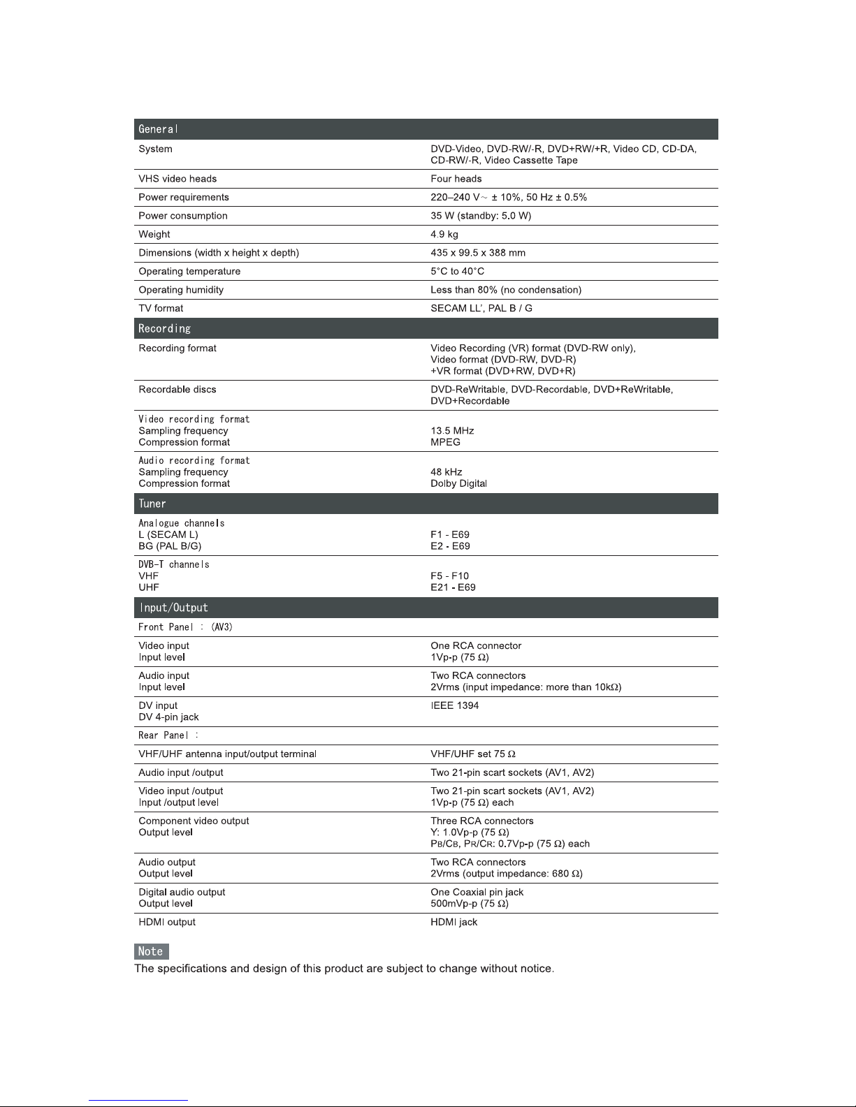
1-1-1 E9NG0SP
SPECIFICATIONS
1-2-1 TD5PLSP
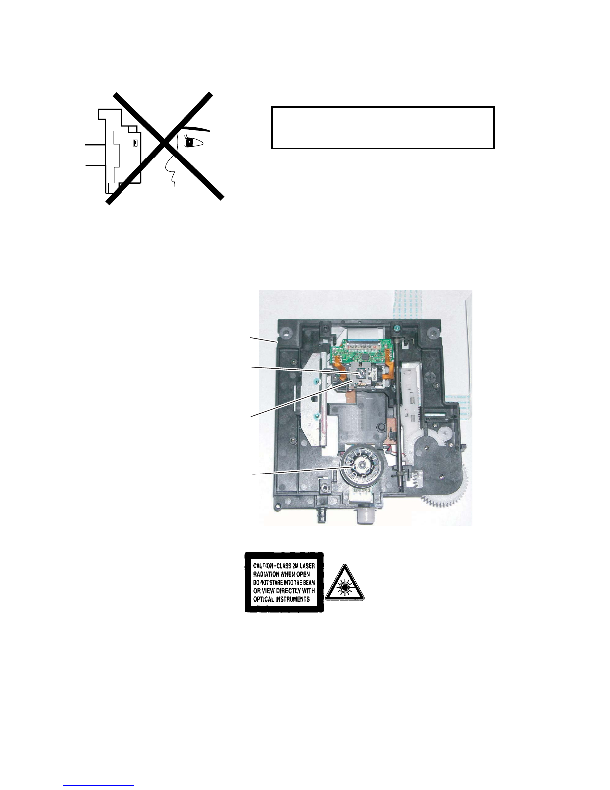
LASER BEAM SAFETY PRECAUTIONS
This DVD player uses a pickup that emits a laser beam.
The laser beam is emitted from the location shown in the figure. When checking the laser diode, be sure to keep
your eyes at least 30 cm away from the pickup lens when the diode is turned on. Do not look directly at the laser
beam.
CAUTION: Use of controls and adjustments, or doing procedures other than those specified herein, may result in
hazardous radiation exposure.
Location: Inside Top of DVD mechanism.
Do not look directly at the laser beam coming
from the pickup or allow it to strike against your
skin.
Drive Mechanism Assembly
Laser Beam Radiation
Laser Pickup
Turntable

1-3-1 DVDP_ISPT
IMPORTANT SAFETY PRECAUTIONS
Product Safety Notice
Some electrical and mechanical parts have special
safety-related characteristics which are often not evident from visual inspection, nor can the protection
they give necessarily be obtained by replacing them
with components rated for higher voltage, wattage,
etc. Parts that have special safety characteristics are
identified by a ! on schematics and in parts lists. Use
of a substitute replacement that does not have the
same safety characteristics as the recommended
replacement part might create shock, fire, and/or other
hazards. The Product’s Safety is under review continuously and new instructions are issued whenever
appropriate. Prior to shipment from the factory, our
products are carefully inspected to confirm with the
recognized product safety and electrical codes of the
countries in which they are to be sold. However, in
order to maintain such compliance, it is equally important to implement the following precautions when a set
is being serviced.
Precautions during Servicing
A. Parts identified by the ! symbol are critical for
safety. Replace only with part number specified.
B. In addition to safety, other parts and assemblies
are specified for conformance with regulations
applying to spurious radiation. These must also be
replaced only with specified replacements.
Examples: RF converters, RF cables, noise blocking capacitors, and noise blocking filters, etc.
C. Use specified internal wiring. Note especially:
1)Wires covered with PVC tubing
2)Double insulated wires
3)High voltage leads
D. Use specified insulating materials for hazardous
live parts. Note especially:
1)Insulation tape
2)PVC tubing
3)Spacers
4)Insulators for transistors
E. When replacing AC primary side components
(transformers, power cord, etc.), wrap ends of
wires securely about the terminals before soldering.
F. Observe that the wires do not contact heat produc-
ing parts (heatsinks, oxide metal film resistors, fusible resistors, etc.).
G. Check that replaced wires do not contact sharp
edges or pointed parts.
H. When a power cord has been replaced, check that
5 - 6 kg of force in any direction will not loosen it.
I. Also check areas surrounding repaired locations.
J. Be careful that foreign objects (screws, solder
droplets, etc.) do not remain inside the set.
K. When connecting or disconnecting the internal
connectors, first, disconnect the AC plug from the
AC outlet.
L. Be sure to confirm the FAN motor has completely
stopped when disconnecting the AC cord for termination processing is activated during inner P-on
immediately after turning Power off.
1-3-2 DVDP_ISPT
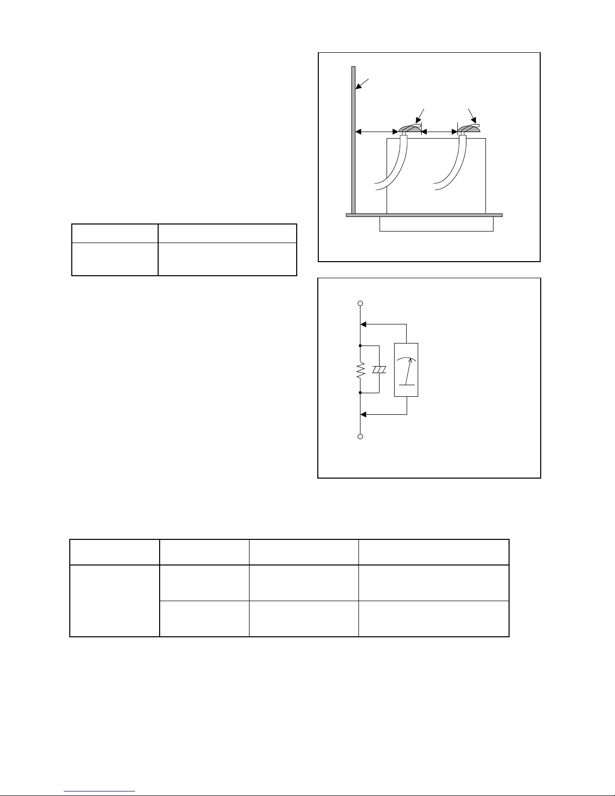
Fig. 1
Chassis or Secondary Conductor
Primary Circuit
d' d
AC Voltmeter
(High Impedance)
Exposed Accessible Part
B
One side of
Power Cord Plug Prongs
Z
Fig. 2
Safety Check after Servicing
Examine the area surrounding the repaired location
for damage or deterioration. Observe that screws,
parts, and wires have been returned to their original
positions. Afterwards, do the following tests and confirm the specified values to verify compliance with
safety standards.
1. Clearance Distance
When replacing primary circuit components, confirm
specified clearance distance (d) and (d’) between soldered terminals, and between terminals and surrounding metallic parts. (See Fig. 1)
Table 1 : Ratings for selected area
Note: This table is unofficial and for reference only.
Be sure to confirm the precise values.
2. Leakage Current Test
Confirm the specified (or lower) leakage current
between B (earth ground, power cord plug prongs)
and externally exposed accessible parts (RF terminals, antenna terminals, video and audio input and
output terminals, microphone jacks, earphone jacks,
etc.) is lower than or equal to the specified value in the
table below.
Measuring Method (Power ON) :
Insert load Z between B (earth ground, power cord
plug prongs) and exposed accessible parts. Use an
AC voltmeter to measure across the terminals of load
Z. See Fig. 2 and the following table.
AC Line Voltage Clearance Distance (d), (d’)
230 V
≥ 3.2 mm(d)
≥ 6.0 mm(d’)
Table 2: Leakage current ratings for selected areas
Note: This table is unofficial and for reference only. Be sure to confirm the precise values.
AC Line Voltage Load Z Leakage Current (i)
One side of power cord plug
prongs (B) to:
230 V
2kΩ RES.
Connected in
parallel
i≤0.7mA AC Peak
i≤2mA DC
RF or
Antenna terminals
50kΩ RES.
Connected in
parallel
i≤0.7mA AC Peak
i≤2mA DC
A/V Input, Output
1-4-1 DVDN_SN
STANDARD NOTES FOR SERVICING
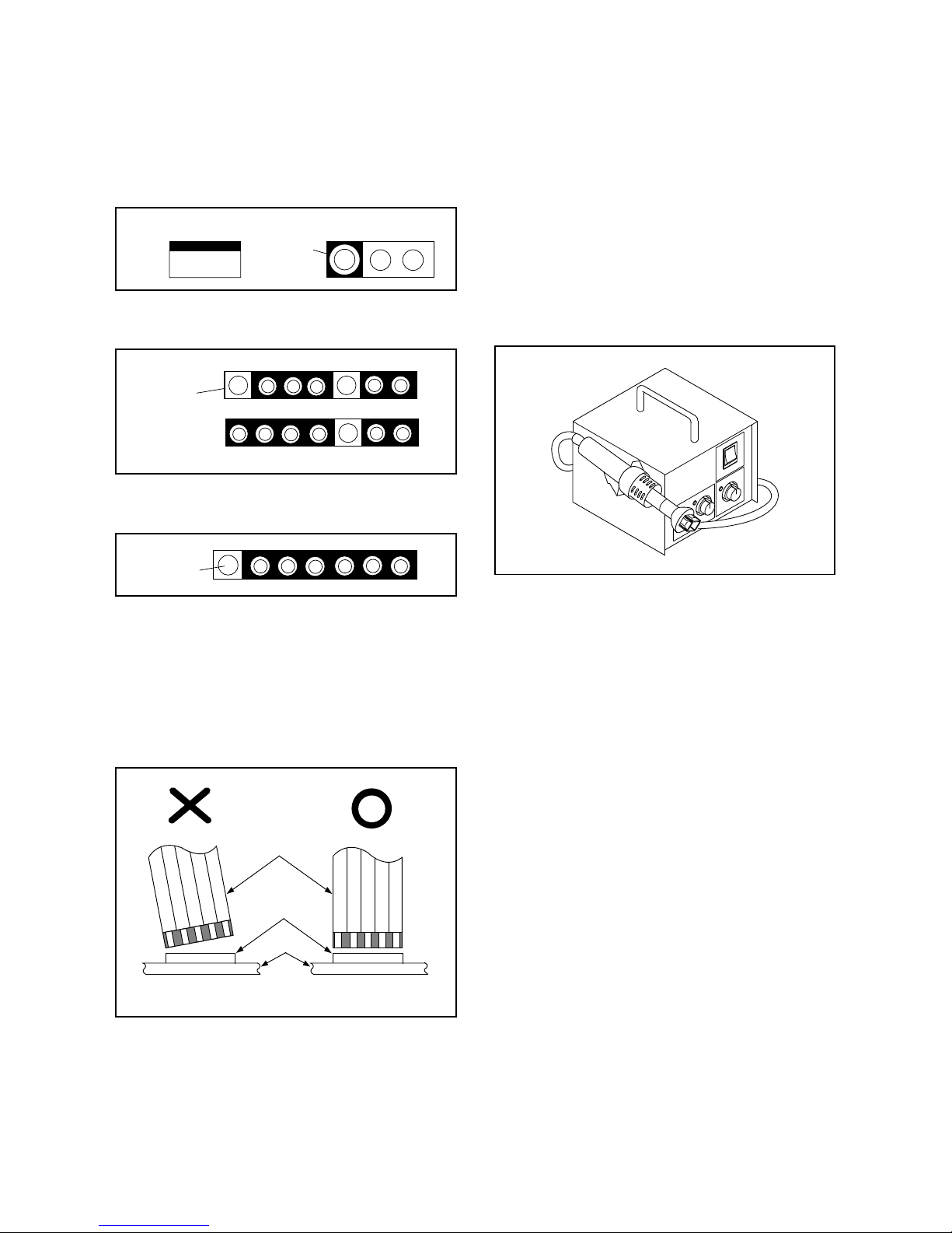
Circuit Board Indications
1. The output pin of the 3 pin Regulator ICs is
indicated as shown.
2. For other ICs, pin 1 and every fifth pin are
indicated as shown.
3. The 1st pin of every male connector is indicated as
shown.
Instructions for Connectors
1. When you connect or disconnect the FFC (Flexible
Foil Connector) cable, be sure to first disconnect
the AC cord.
2. FFC (Flexible Foil Connector) cable should be
inserted parallel into the connector, not at an
angle.
Pb (Lead) Free Solder
When soldering, be sure to use the Pb free solder.
How to Remove / Install Flat Pack-IC
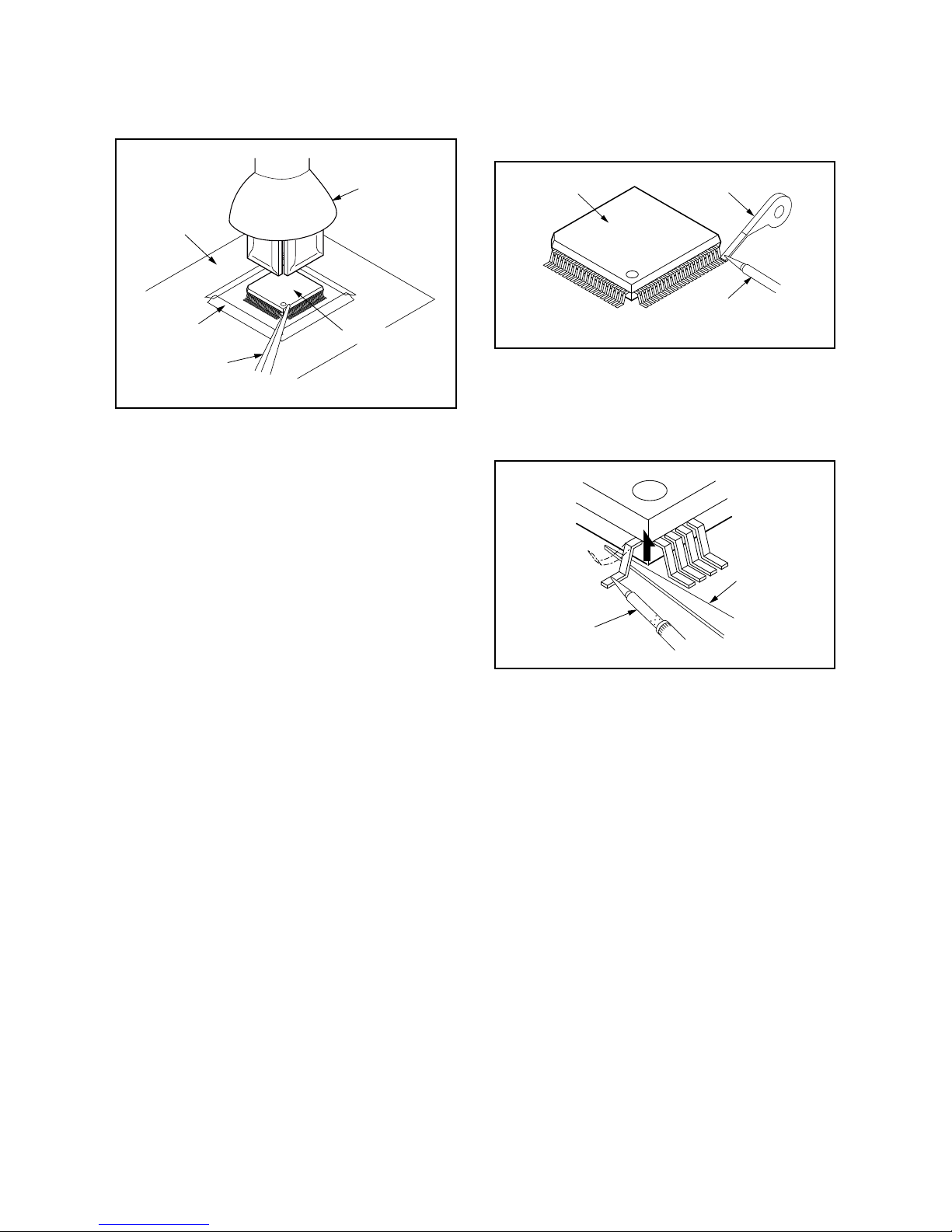
1. Removal
With Hot-Air Flat Pack-IC Desoldering Machine:
1. Prepare the hot-air flat pack-IC desoldering
machine, then apply hot air to the Flat Pack-IC
(about 5 to 6 seconds). (Fig. S-1-1)
2. Remove the flat pack-IC with tweezers while
applying the hot air.
3. Bottom of the flat pack-IC is fixed with glue to the
BOARD; when removing entire flat pack-IC, first
apply soldering iron to center of the flat pack-IC
and heat up. Then remove (glue will be melted).
(Fig. S-1-6)
4. Release the flat pack-IC from the BOARD using
tweezers. (Fig. S-1-6)
CAUTION:
1. The Flat Pack-IC shape may differ by models. Use
an appropriate hot-air flat pack-IC desoldering
machine, whose shape matches that of the Flat
Pack-IC.
2. Do not supply hot air to the chip parts around the
flat pack-IC for over 6 seconds because damage
to the chip parts may occur. Put masking tape
around the flat pack-IC to protect other parts from
damage. (Fig. S-1-2)
NOTE: BOARD MEANS PRINTED CIRCUIT BOARD.
Top View
Out
In
Bottom View
Input
5
10
Pin 1
Pin 1
FFC Cable
Connector
BOARD
* Be careful to avoid a short circuit.
Fig. S-1-1
1-4-2 DVDN_SN
3. The flat pack-IC on the BOARD is affixed with
glue, so be careful not to break or damage the foil
of each pin or the solder lands under the IC when
removing it.
With Soldering Iron:
1. Using desoldering braid, remove the solder from
all pins of the flat pack-IC. When you use solder
flux which is applied to all pins of the flat pack-IC,
you can remove it easily. (Fig. S-1-3)
2. Lift each lead of the flat pack-IC upward one by
one, using a sharp pin or wire to which solder will
not adhere (iron wire). When heating the pins, use
a fine tip soldering iron or a hot air desoldering
machine. (Fig. S-1-4)
3. Bottom of the flat pack-IC is fixed with glue to the
BOARD; when removing entire flat pack-IC, first
apply soldering iron to center of the flat pack-IC
and heat up. Then remove (glue will be melted).
(Fig. S-1-6)
4. Release the flat pack-IC from the BOARD using
tweezers. (Fig. S-1-6)
Hot-air
Flat Pack-IC
Desoldering
Machine
BOARD
Flat Pack-IC
Tweezers
Masking
Tape
Fig. S-1-2
Flat Pack-IC
Desoldering Braid
Soldering Iron
Fig. S-1-3
Fine Tip
Soldering Iron
Sharp
Pin
Fig. S-1-4

1-4-3 DVDN_SN
With Iron Wire:
1. Using desoldering braid, remove the solder from
all pins of the flat pack-IC. When you use solder
flux which is applied to all pins of the flat pack-IC,
you can remove it easily. (Fig. S-1-3)
2. Affix the wire to a workbench or solid mounting
point, as shown in Fig. S-1-5.
3. While heating the pins using a fine tip soldering
iron or hot air blower, pull up the wire as the solder
melts so as to lift the IC leads from the BOARD
contact pads as shown in Fig. S-1-5.
4. Bottom of the flat pack-IC is fixed with glue to the
BOARD; when removing entire flat pack-IC, first
apply soldering iron to center of the flat pack-IC
and heat up. Then remove (glue will be melted).
(Fig. S-1-6)
5. Release the flat pack-IC from the BOARD using
tweezers. (Fig. S-1-6)
Note: When using a soldering iron, care must be
taken to ensure that the flat pack-IC is not
being held by glue. When the flat pack-IC is
removed from the BOARD, handle it gently
because it may be damaged if force is applied.
2. Installation
1. Using desoldering braid, remove the solder from
the foil of each pin of the flat pack-IC on the
BOARD so you can install a replacement flat packIC more easily.
2. The “●” mark on the flat pack-IC indicates pin 1.
(See Fig. S-1-7.) Be sure this mark matches the 1
on the BOARD when positioning for installation.
Then presolder the four corners of the flat pack-IC.
(See Fig. S-1-8.)
3. Solder all pins of the flat pack-IC. Be sure that
none of the pins have solder bridges.
To Solid
Mounting Point
Soldering Iron
Iron Wire
or
Hot Air Blower
Fig. S-1-5
Fine Tip
Soldering Iron
BOARD
Flat Pack-IC
Tweezers
Fig. S-1-6
Example :
Pin 1 of the Flat Pack-IC
is indicated by a " " mark.
Fig. S-1-7
Presolder
BOARD
Flat Pack-IC
Fig. S-1-8
1-4-4 DVDN_SN
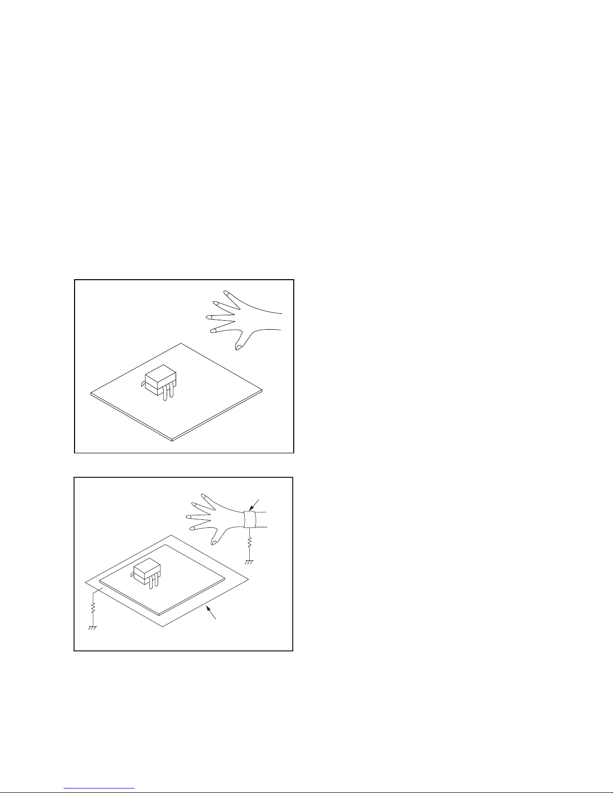
Instructions for Handling Semiconductors
Electrostatic breakdown of the semi-conductors may
occur due to a potential difference caused by
electrostatic charge during unpacking or repair work.
1. Ground for Human Body
Be sure to wear a grounding band (1 MΩ) that is
properly grounded to remove any static electricity that
may be charged on the body.
2. Ground for Workbench
Be sure to place a conductive sheet or copper plate
with proper grounding (1 MΩ) on the workbench or
other surface, where the semi-conductors are to be
placed. Because the static electricity charge on
clothing will not escape through the body grounding
band, be careful to avoid contacting semi-conductors
with your clothing.
<Incorrect>
BOARD
Grounding Band
Conductive Sheet or
Copper Plate
1MΩ
1MΩ
<Correct>
BOARD
1-5-1 E9NG0PFS
PREPARATION FOR SERVICING
How to Enter the Service Mode
About Optical Sensors
Caution:
An optical sensor system is used for the Tape Start
and End Sensors on this equipment. Carefully read
and follow the instructions below. Otherwise the unit
may operate erratically.
What to do for preparation
Insert a tape into the Deck Mechanism Assembly and
press [VCR PLAY] button. The tape will be loaded into
the Deck Mechanism Assembly. Make sure the power
is on, connect J303 to GND. This will stop the function
of Tape Start Sensor, Tape End Sensor and Reel Sensors. (If these TPs are connected before plugging in
the unit, the function of the sensors will stay valid.)
See Fig. 1.
Note: Because the Tape End Sensors are inactive, do
not run a tape all the way to the start or the end of the
tape to avoid tape damage.
Q504
Q503
J917 (S-INH)
Fig. 1
1-6-1 E9NG0DC
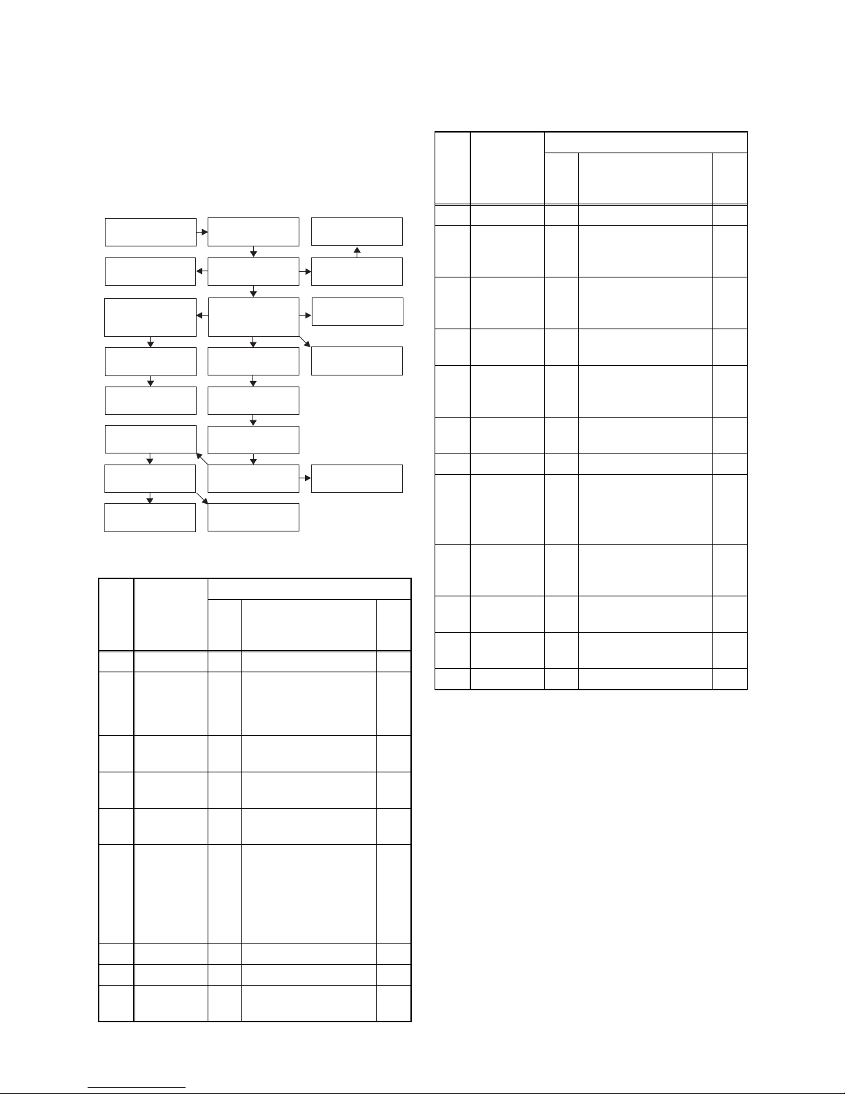
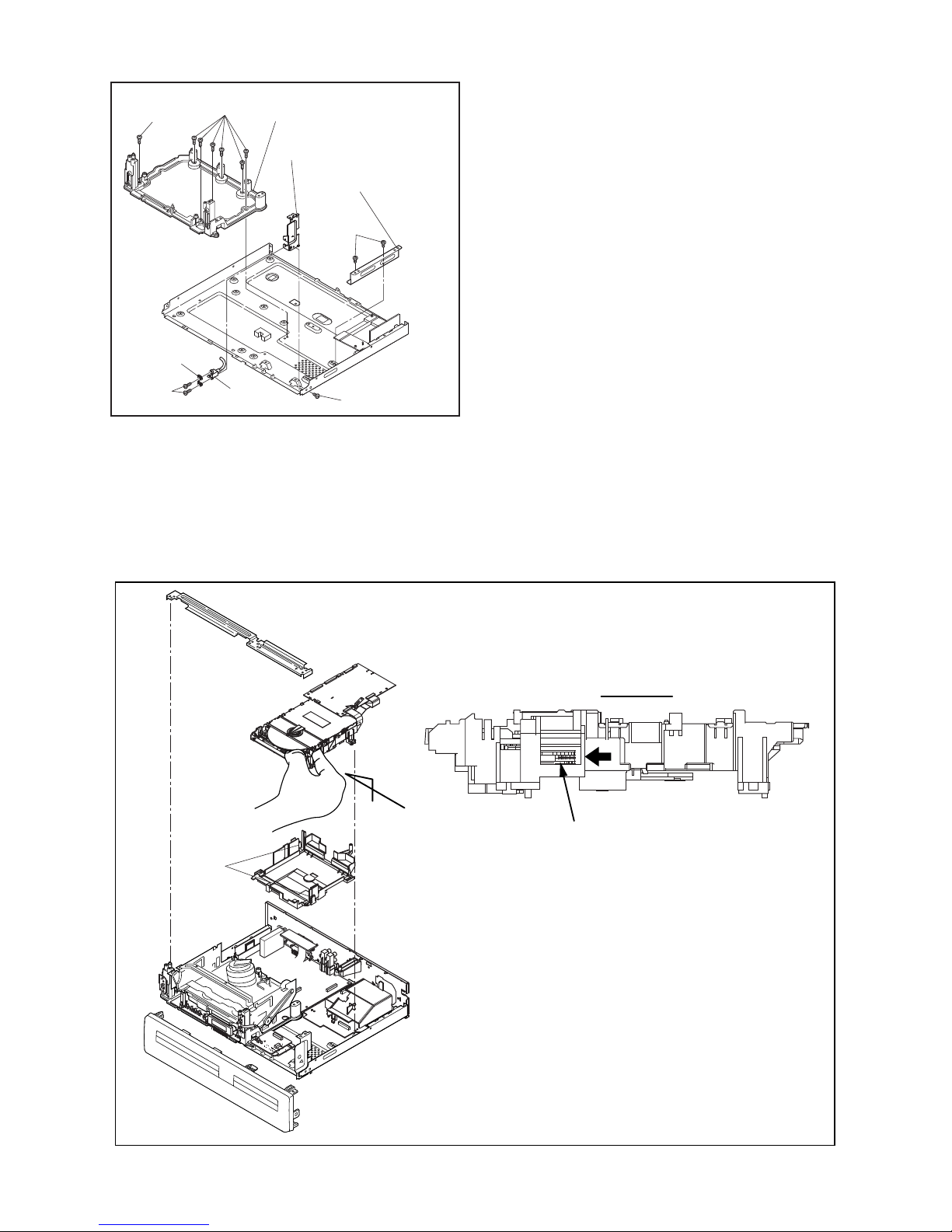
CABINET DISASSEMBLY INSTRUCTIONS
1. Disassembly Flowchart
This flowchart indicates the disassembly steps to gain
access to item(s) to be serviced. When reassembling,
follow the steps in reverse order. Bend, route, and
dress the cables as they were originally.
2. Disassembly Method
Note:
(1): Identification (location) No. of parts in the figures
(2): Name of the part
(3): Figure Number for reference
(4): Identification of parts to be removed, unhooked,
unlocked, released, unplugged, unclamped, or
desoldered.
P=Spring, L=Locking Tab, S=Screw,
CN=Connector
*=Unhook, Unlock, Release, Unplug, or Desolder
e.g. 6(S-1) = six Screws (S-1),
5(L-1) = five Locking Tabs (L-1)
(5): Refer to “Reference Notes.”
NOTE: BOARD MEANS PRINTED CIRCUIT BOARD.
ID/
LOC.
No.
PART
REMOVAL
Fig.
No.
REMOVE/*UNHOOK/
UNLOCK/RELEASE/
UNPLUG/DESOLDER
Note
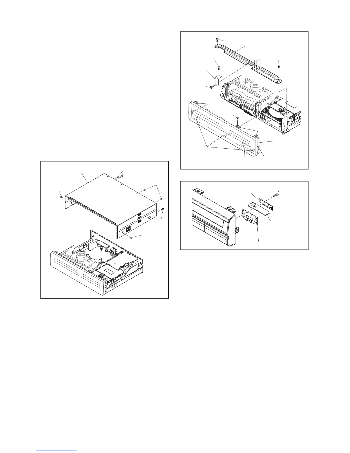
[1] Cover Top D1 7(S-1) ---
[2] Panel Front D2
(S-2), *5(L-1), *3(L-2),
*CN1231
1
1-1
1-2
1-3
[3]
Front
Bracket
D2
3(S-3), (S-4), Front
Support
---
[4]
Jack
Bracket
D3 (S-5) ---
[5]
BOARD
Front Jack
D3 Jack Plate Earth ---
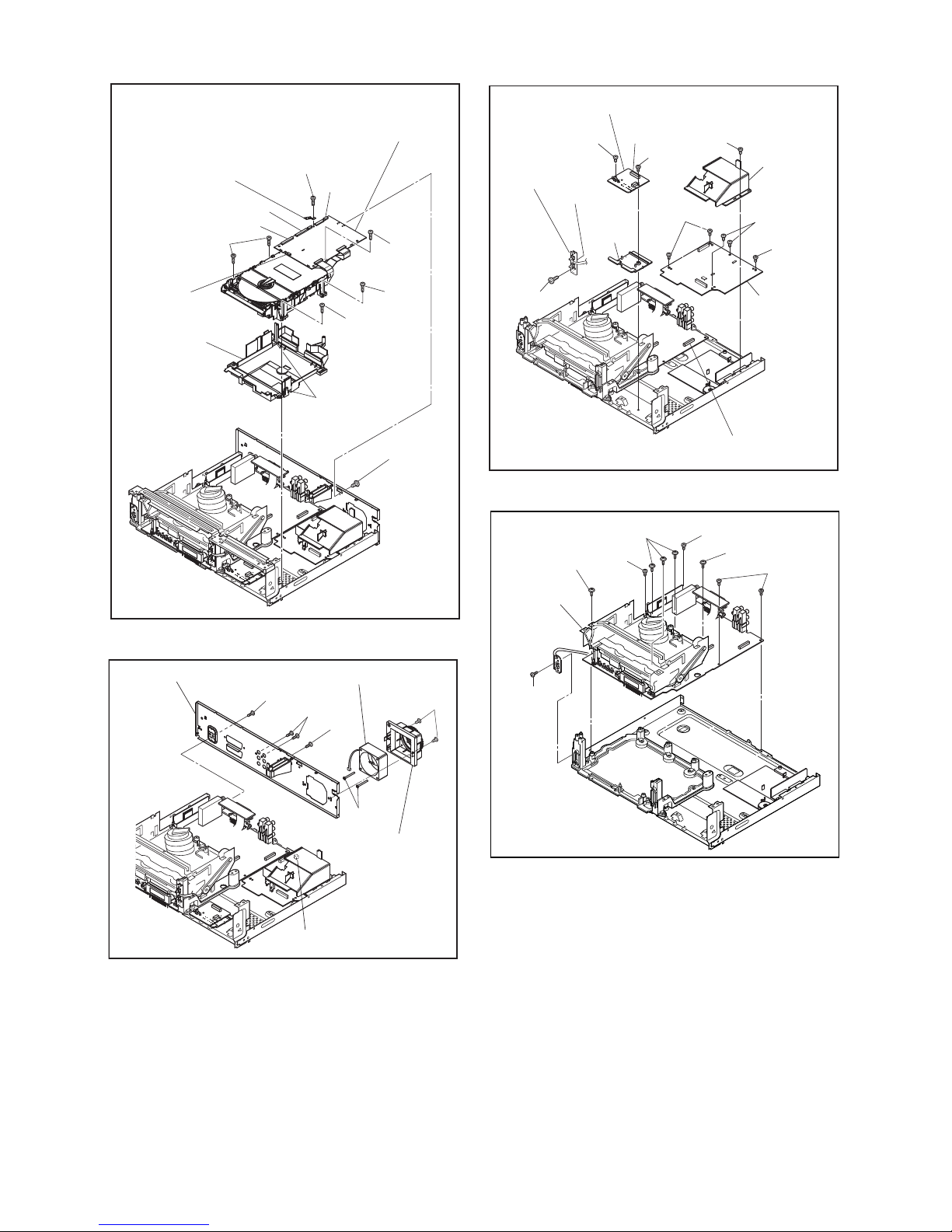
[6]
DVD
Mechanism
& DVD
Main
BOARD
Assembly
D4
(S-6), 2(S-7), 2(S-8),
2(S-9), *CN101,
*CN502-D, *CN701,
*CN901, Mecha Plate
Earth
4
[7] Dust Cover D4 Hook ---
[8] Fan Holder D5 2(S-10), *CN1002 ---
[9]
Motor DC
Fan
D5 2(S-11) ---
[1] Cover Top
[2] Panel
Front
[3] Front
Bracket
[4] Jack
Bracket
[20] Front
Bracket R
[21] Bracket R
[5] BOARD
Front Jack
[13] BOARD
Function
[6] DVD Mechanism
& DVD Main
BOARD Assembly
[7] Dust Cover
[11] BOARD
Power
Supply
[12] BOARD
Switch
[8] Fan Holder
[9] Motor DC
Fan
[10] Panel Rear
[15] Deck
Assembly
[19] Deck
Pedestal
[14] VCR
Chassis Unit
[18] BOARD
Power Switch
[16] BOARD
AV
[17] BOARD
DTV Module Unit
[10] Panel Rear D5 2(S-12), 2(S-13) ---
[11]
BOARD
Power
Supply
D6
(S-14), 3(S-15),
2(S-16), *CN1503,
FFC Guide
---
[12]
BOARD
Switch
D6
(S-17), (S-18),
*CN3001, Front
Pedestal
---
[13]
BOARD
Function
D6 (S-19), Desolder ---
[14]
VCR
Chassis
Unit
D7
5(S-20), 4(S-21),
(S-22)
---
[15]
Deck
Assembly
D8
(S-23), (S-24), (S-25)
Desolder
2
3
[16] BOARD AV D8 ---------- ---
[17]
BOARD
DTV
Module
Unit
D8 Desolder ---
[18]
BOARD
Power
Switch
D8 Desolder ---
[19]
Deck
Pedestal
D9 7(S-26) ---
[20]
Front
Bracket R
D9
(S-27), 2(S-28), DV
Cable, DV Plate Earth
---
[21] Bracket R D9 2(S-29) ---
↓
(1)
↓
(2)
↓
(3)
↓
(4)
↓
(5)
ID/
LOC.
No.
PAR T
REMOVAL
Fig.
No.
REMOVE/*UNHOOK/
UNLOCK/RELEASE/
UNPLUG/DESOLDER
Note
1-6-2 E9NG0DC
Reference Notes
CAUTION 1: Locking Tabs (L-1) and (L-2) are fragile.
Be careful not to break them.
1-1. Release five Locking Tabs (L-1).
1-2. Release three Locking Tabs (L-2).
1-3. Disconnect Connector (CN1231) and remove the
Panel Front.
2. When reassembling, solder wire jumpers as shown
in Fig. D8.
3. Before installing the Deck Assembly, be sure to
place the pin of LD-SW on BOARD AV as shown in
Fig. D8. Then, install the Deck Assembly while
aligning the hole of Cam Gear with the pin of LDSW, the shaft of Cam Gear with the hole of LD-SW
as shown in Fig. D8.
4. The DVD Mechanism & DVD Main BOARD
Assembly is adjusted as a unit at factory.
Therefore, do not disassemble it.
Replace the DVD Mechanism & DVD Main
BOARD Assembly as a unit.
(S-1)
(S-1)
(S-1)
(S-1)
(S-1)
[1] Cover Top
Fig. D1
(S-3)
(S-3)
(L-1)
(L-2)
(L-1)
(S-4)
(S-3)
(S-2)
CN1231
(L-1)
Fig. D2
Front
Support
[2] Panel
Front
[3] Front Bracket
Fig. D3
(S-5)
Jack Plate Earth
[4] Jack Bracket
[5] BOARD
Front Jack
1-6-3 E9NG0DC
(S-9)
CN101
CN901
CN701
Mecha Plate
Earth
CN502-D
(S-7)
(S-6)
Hook
Fig. D4
[6] DVD Mechanism &
DVD Main BOARD
Assembly
[7] Dust Cover
(S-8)
(S-8)
(S-7)
(S-10)
(S-12)
(S-13)
(S-12)
(S-11)
Fig. D5
[9] Motor DC Fan
[8] Fan Holder
[10] Panel Rear
CN1002
(S-14)
FFC Guide
(S-17)
(S-18)
(S-16)
(S-15)
(S-15)
(S-19)
CN1503
CN3001
Fig. D6
[11] BOARD
Power
Supply
[12] BOARD Switch
[13] BOARD
Function
Desolder
Front
Pedestal
(S-20)
(S-20)
(S-20)
(S-21)
(S-21)
(S-22)
(S-21)
Fig. D7
[14] VCR
Chassis
Unit
1-6-4 E9NG0DC
[16] BOARD AV
[17]
BOARD DTV
Module Unit
[15] Deck
Assembly
[18] BOARD
Power Switch
FE Head
Cylinder
Assembly
ACE Head
Assembly
Desolder
Lead with
blue stripe
[16] BOARD AV
SW507
LD-SW
From
FE Head
BOTTOM VIEW
Lead connections of Deck Assembly and BOARD AV
Desolder
From
Capstan
Motor
Assembly
Printing side
Desolder
Desolder
Desolder
From
Cylinder
Assembly
From
ACE Head
Assembly
Lead with
blue stripe
Lead with
black stripe
(S-23)
(S-24)
(S-25)
Fig. D8
LD-SW
Pin
Pin
Hole
Hole
Shaft
Cam Gear
[16] BOARD AV
[15] Deck Assembly
Pin
1-6-5 E9NG0DC
3. How to Eject Manually
Note: When rotating the gear, be careful not to damage the gear.
1. Remove the Cover Top, Panel Front, Front Bracket, DVD Mechanism & DVD Main BOARD Assembly.
2. Remove the Dust Cover.
3. Rotate the gear in the direction of the arrow manually as shown below.
4. Pull the tray out manually and remove a disc.
(S-26)
(S-26)
(S-27)
(S-28)
DV PlateEarth
DV Cable
(S-29)
Fig. D9
[19] Deck Pedestal
[21] Bracket R
[20] Front Bracket R
Rotate this gear in
the direction of the arrow
Hook
View for A
A
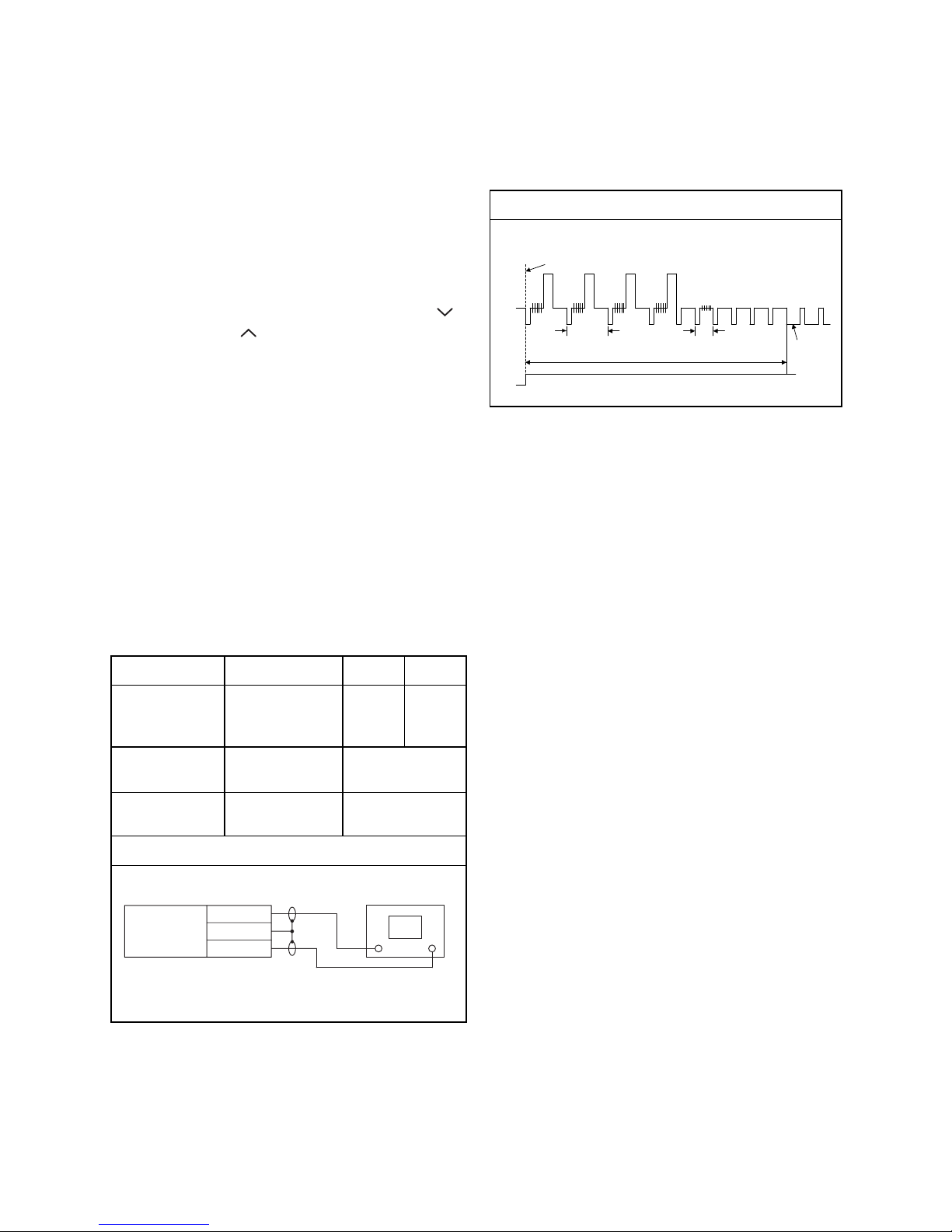
1-7-1 E9NG0EA
ELECTRICAL ADJUSTMENT INSTRUCTIONS
NOTE:
1.Electrical adjustments are required after replacing
circuit components and certain mechanical parts.
It is important to do these adjustments only after
all repairs and replacements have been completed. Also, do not attempt these adjustments
unless the proper equipment is available.
2.To perform these alignment / confirmation procedures, make sure that the tracking control is set in
the center position: Press either [PROGRAM 5??]
or [PROGRAM ] button on the front panel first,
then the [ O ] (VCR) button on the front panel.
Test Equipment Required
1.Oscilloscope: Dual-trace with 10:1 probe,
V-Range: 0.001~50V/Div.,
F-Range: DC~AC-20MHz
2.Alignment Tape (FL6A)
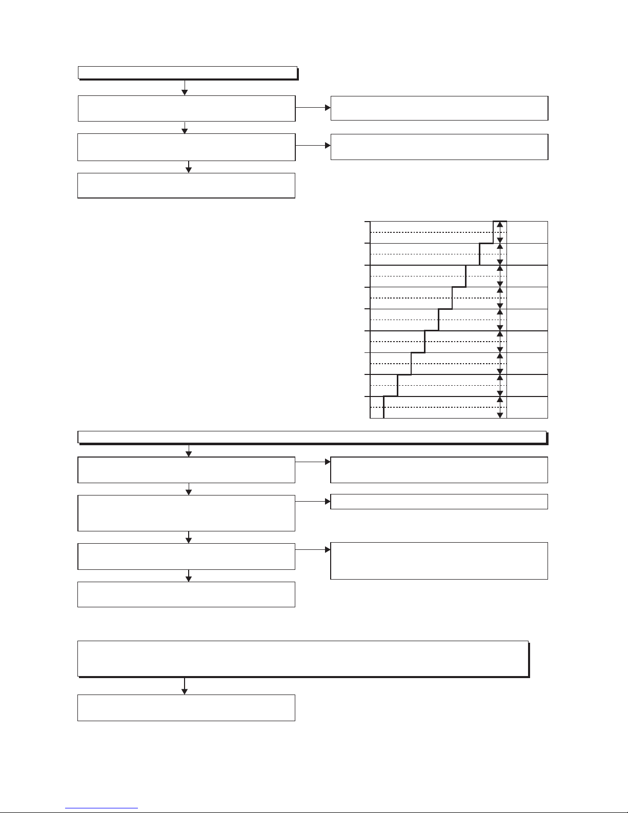
Head Switching Position Adjustment
Purpose:
To determine the Head Switching position during
playback.
Symptom of Misadjustment:
May cause Head Switching noise or vertical jitter
in the picture.
Reference Notes:
Playback the Alignment tape and adjust VR501 so that
the V-sync front edge of the CH1 video output waveform is at the 6.5H±1H (416μs±64μs) delayed position
from the rising edge of the CH2 head switching pulse
waveform.
NOTE: BOARD MEANS PRINTED CIRCUIT BOARD.
Test point Adj.Point Mode Input
J184(
AV1-V-OUT
)
TP504(RF-SW)
GND
VR501
(Switching Point)
(BOARD AV)
PLAY
(SP)
-----
Tape
Measurement
Equipment
Spec.
FL6A Oscilloscope
6.5H±1H
(416μs±64μs)
Connections of Measurement Equipment
Oscilloscope
BOARD
AV
J184
CH1 CH2
Trig. (+)
GND
TP504
Figure 1
EXT. Syncronize Trigger Point
1.0H
CH1
CH2
Switching Pulse
V-Syn c
0.5H
6.5H±1H (416 μs ± 64 μs)

1-8-1 E9NG0INT
HOW TO INITIALIZE THE DVD RECORDER & VCR
To put the program back at the factory-default, initialize the DVD recorder & VCR as the following procedure.
< DVD Section >
1. Turn the DVD recorder on.
2. Confirm that no disc is loaded or that the disc tray
is open. To put the DVD recorder into the Version
display mode, press [DVD], [INSTANT SKIP], [1],
[2], and [3] buttons on the remote control unit in
that order.
Fig. a appears on the screen.
3. Press [ENTER] button, then the DVD recorder
starts initializing. When the initializing is
completed, the DVD recorder exits the Version
display mode and turns off the power
automatically.
* To move into the Normal mode from the
Version display mode, press [RETURN] button
on the remote control unit instead of [ENTER]
button.
* When [ ] button is pressed before [ENTER]
button is pressed, the DVD recorder exits the
Version display mode, then the power turns
off.
MODEL NAME :
DVB-T VERSION:
FE VERSION :
BE VERSION :
TT VERSION :
DV UNIQUE ID:
LD ADJUSTMENT :
DISC ADJUSTMENT :
DEFAULT SETTING : ENTER
EXIT : RETURN
OK
OK
******
0.23
R50_005_082
WD5******Z2B
T50015FSU
FFFFFFFF FFFFFFFF
*1: "
*******
" differs depending on the models.
*2: Firmware Version differs depending on the
models, and this indication is one example.
Fig. a Version Display Mode Screen
F/W VERSION DISP
1-9-1 E9NG0FW
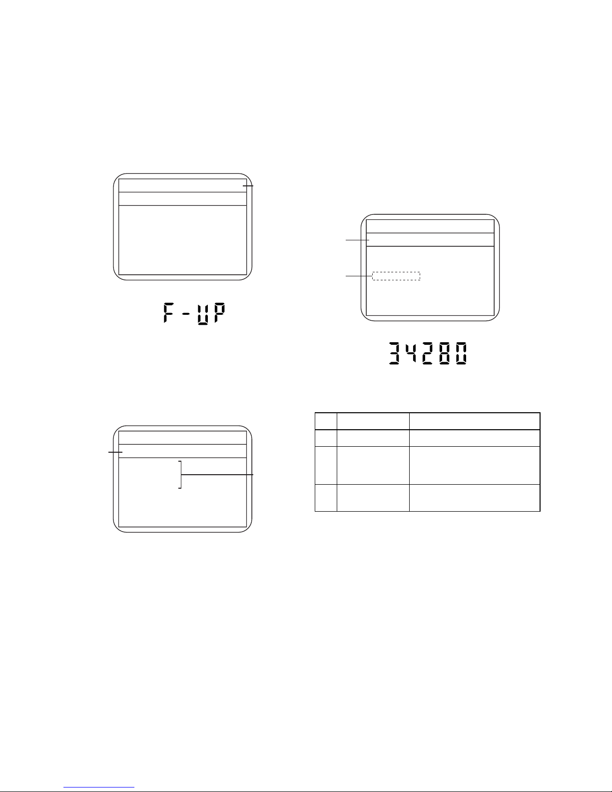
FIRMWARE RENEWAL MODE
1. Turn the power on and remove the disc on the tray.
2. To put the DVD recorder into version up mode,
press [INSTANT SKIP], [6], [5], and [4] buttons on
the remote control unit in the order. Then the tray
will open automatically.
Fig. a appears on the screen and Fig. b appears
on the VFD.
3. Load the disc for version up.
Fig. c appears on the screen. The file on the top is
highlighted as the default.
When there is only one file to exist, Step 4 will
start automatically.
4. Select the firmware version pressing arrow
buttons, then press [ENTER].
Fig. d appears on the screen and Fig. e appears
on the VFD. The DVD recorder starts updating.
About VFD indication of Fig. e:
1) When Fig. d is displayed on the screen, “F-UP”
is displayed on the VFD.
2) When “Firmware Updating... XX% Complete.”
is displayed on the screen, “34280” is displayed
on the VFD.
The appearance shown in (*1) of Fig. d is
described as follows.
5. After updating is finished, the tray opens
automatically.
At this time, no button is available.
6. Pull out the AC code once, then insert it again.
Fig. a Version Up Mode Screen
* Firmware Version differs depending on the
models, and this indication is one example.
Current
F/W version
is displayed.
Firm Update Mode
Please insert a disc.
ver. WD5T*****X2G
Fig. b VFD in Version Up Mode
Fig. c Update Disc Screen
* Firmware Version differs depending on the
models, and this indication is one example.
Disc name
is displayed.
Firm Update Mode ver. WD5T*****X2G
VOL_200804130934
1 WD5T34280X2G
2 WD5T34281X2G
3 WD5T34282X2G
4 WD5T34283X2G
1 / 1
Files included
in the disc are
displayed.
No. Appearance State
1 File Loading... Sending files into the memory
2
Firmware
Updating...
XX% Complete.
Writing new version data
---
Firmware
Update Failure
Failed in updating
Fig. d Programming Mode Screen
* Firmware Version differs depending on the
models, and this indication is one example.
Selected
F/W Version
is displayed.
Firm Update Mode
ver.
WD5T*****X2G
WD5T34280X2G
File Loading...
(*1)
Fig. e VFD in Programming Mode (Example)
1-9-2 E9NG0FW
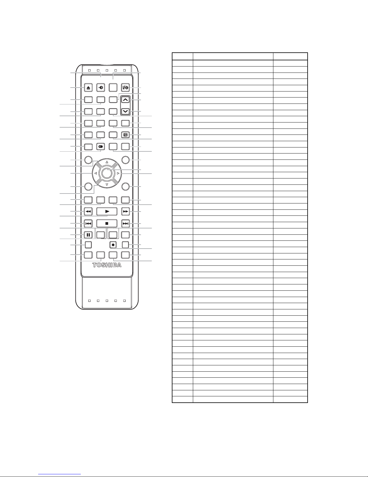
REMOTE CONTROL KEY CODE
NEC Format
Key No. Name Code
1 OPEN/CLOSE 45BC-11
2 INPUT SELECT 45BC-0F
3 HDMI 45BC-B0
4 ON/STANDBY 45BC-12
51 45BC-01
62 45BC-02
73 45BC-03
8PROG. UP 45BC-1E
94 45BC-04
10 5 45BC-05
11 6 45BC-06
12 PROG. DOWN 45BC-1F
13 7 45BC-07
14 8 45BC-08
15 9 45BC-09
16 TIME SLIP 45BC-1A
17 SAT.LINK 45BC-1D
18 0 45BC-00
19 CLEAR 45BC-53
20 INFO 45BC-3F
21 TEXT 45BC - 23
22 AUDIO 45BC-D3
23 SUBTITLE 45BC-D5
24 GUIDE 45BC-6D
25 TOP MENU 45BC-D0
26 CURSOR UP 45BC-C0
27 DISC MENU 45BC-D1
28 CURSOR LEFT 45BC-CC
29 ENTER 45BC-44
30 CURSOR RIGHT 45BC-C4
31 DISPLAY 45BC-5A
32 CURSOR DOWN 45BC-C8
33 RETURN 45BC-D2
34 RED 45BC-2A
35 GREEN 45BC-2B
36 YELLOW(MODE) 45BC-2C
37 BLUE(SEARCH) 45BC-29
38 REV 45BC-98
39 PLAY 45BC-13
40 FWD 45BC-9A
41 SKIP DOWN 45BC-84
42 STOP 45BC-16
43 SKIP UP 45BC-80
44 PAUSE 45BC-17
45 VCR 45BC-1B
46 DVD 45BC-18
47 INSTANT SKIP 45BC-5B
48 DUBBING 45BC-56
49 --- ---
50 REC 45BC-15
51 REC MODE 45BC-A7
52 SETUP 45BC-52
53 TIMER SET 45BC-67
54 TIMER PROG. 45BC-40
55 1.3x/0.8x PLAY 45BC-AA
.OO/:
OPEN/
CLOSE
INPUT
SELECT
HDMI
ABC DEF
GHI JKL MNO PROG.
PQRS T UV WXYZ TIME SLIP
SAT.LINK SPACE CLEAR INFO
TEXT AUDIO SUBTITLE GUIDE
TOP MENU DISC MENU
ENTER
DISPLAY RETURN
MODE SEARCH
REV PLAY FWD
SKIP STOP SKIP
PAUSE VCR DVD
INSTANT SKIP
DUBBING REC REC MODE
SETUP
TIMER SET
SE-R0306
TIMER PROG. 1.3x/0.8xPLAY
1203
456
789
1
9
20
24
27
33
51
50
46
23
37
36
16
19
15
30
11
40
43
47
54
55
29
22
25
17
21
31
38
41
44
52
48
28
35
34
45
6
10
39
42
53
2
3
4
7
8
12
13
14
5
18
26
32

1-10-1 E9NG0TR
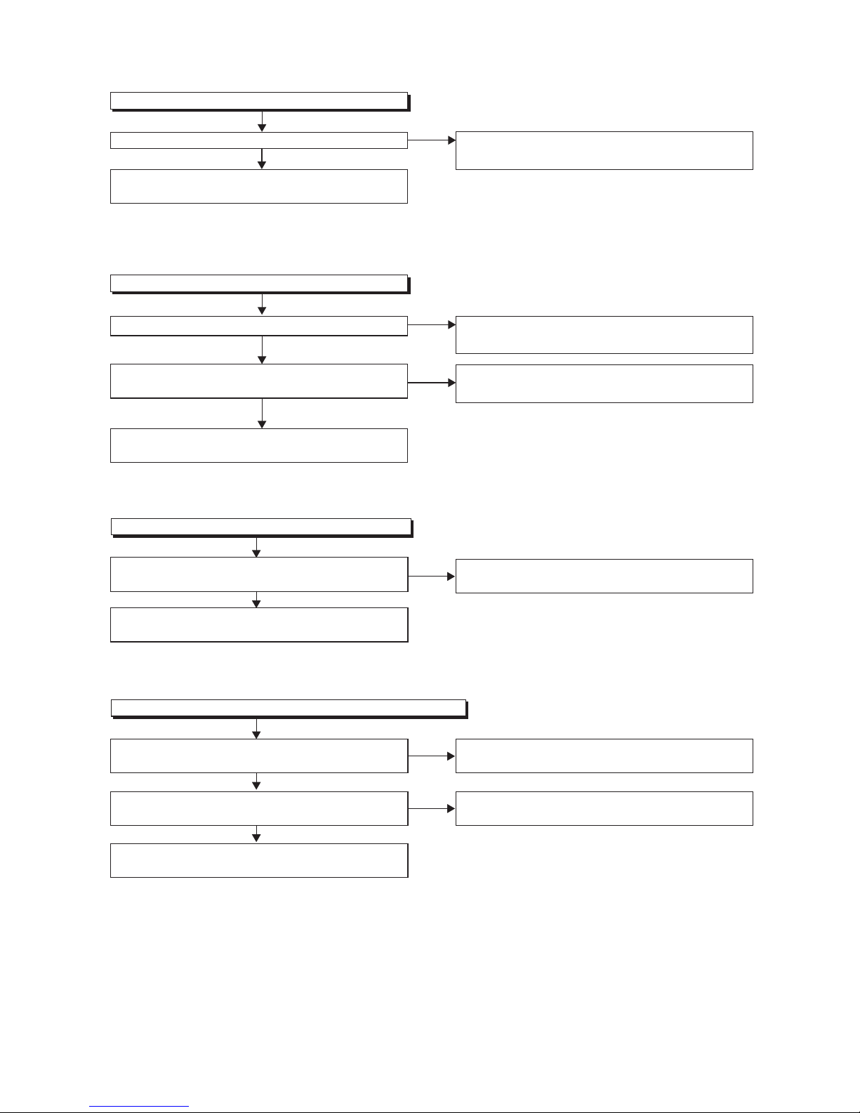
TROUBLESHOOTING
1 Power Supply Section
NOTE: BOARD MEANS PRINTED CIRCUIT BOARD.
FLOW CHART NO.1
The power cannot be turned on.
Is the fuse normal?
Is normal state restored when once unplugged
power cord is plugged again after several seconds.
Is the AL+5V line voltage normal?
Check each rectifying circuit of secondary circuit
and replace P1(AV ASSEMBLY) if defective.
See FLOW CHART No.2 <The fuse blows out.>
Check for lead or short-circuiting of primary
circuit component and replace P3(PW/SW
ASSEMBLY) if defective.
(Q1001, Q1003, T1001, D1001, D1002, D1003,
D1004, R1043)
Ye s
Ye s
Ye s
No
No
No
FLOW CHART NO.2
The fuse blows out.
After servicing, replace the fuse.
Check the presence that the primary component
is leaking or shorted and replace P3(PW/SW
ASSEMBLY) if defective.
Check the presence that the rectifying diode or circuit
is shorted in each rectifying circuit of secondary side
and replace P3(PW/SW ASSEMBLY) if defective.
FLOW CHART NO.3
When the output voltage fluctuates.
No
Ye s
Does the secondary side photo coupler circuit
operate normally?
Check the circuit and replace P3(PW/SW
ASSEMBLY) if defective.
(IC1001, D1006, D1012, D1024)
Check the circuit and replace P3(PW/SW
ASSEMBLY) if defective.
(IC1001, Q1004, D015, D017, D1019)
FLOW CHART NO.4
When buzz sound can be heard in the vicinity of power circuit.
Check if there is short circuit on the rectifying diode and the circuit in each rectifying circuit of secondary side,
and replace P1(AV ASSEMBLY) if defective. (D013, D014, D016, D018, D019, D1008, D1016, D1030, D1031,
D1032, IC1103, IC1104, IC1800, Q1100, Q1105, Q1106, Q1110, Q1114, Q1508, Q1511, Q1513, Q1516,
Q1517, Q1520, Q1521, Q1527)
No
Ye s
FLOW CHART NO.5
-FL is not outputted.
Is the supply voltage of -24V fed to the anode of
D018?
Check D018 and their periphery, and replace
P3(PW/SW ASSEMBLY) if defective.
Check for load circuit short-circuiting or leak, and
replace P1(AV ASSEMBLY) if defective.
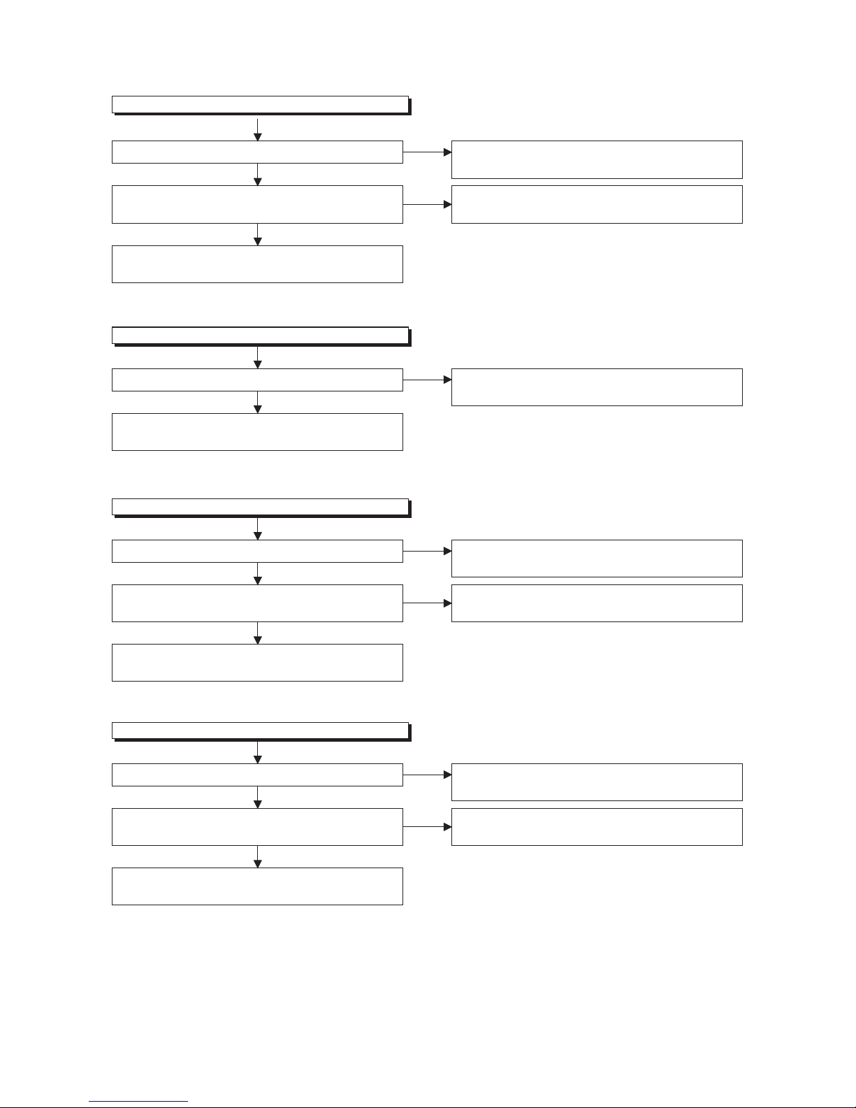
1-10-2 E9NG0TR
No
No
No
No
No
No
Ye s
Ye s
Ye s
Ye s
Ye s
Ye s
FLOW CHART NO.6
P-ON+15V is not outputted.
Is the supply voltage 44V fed to the cathode of D013?
Check D013 and their periphery, and replace
P3(PW/SW ASSEMBLY) if defective.
Check for load circuit short-circuiting or leak, and
replace P1(AV ASSEMBLY) if defective.
FLOW CHART NO.8
AL+12V is not outputted.
Is the supply voltage 12V fed to the cathode of D014?
Check D014 and their periphery, and replace
P3(PW/SW ASSEMBLY) if defective.
Check for load circuit short-circuiting or leak, and
replace P1(AV ASSEMBLY) if defective.
FLOW CHART NO.7
TU+30V is not outputted.
Is 44V voltage supplied to emitter of Q1511?
Refer to "FLOW CHART NO.6"<P-ON+15V is not
outputted>.
Is the "H" pulse (approximately 5V) inputted to
the base of Q1512?
Check the P-ON-H siganal line, and replace
P1(AV ASSEMBLY) if defective.
Check Q1511, Q1512 and their periphery, and
replace P1(AV ASSEMBLY) if defective.
FLOW CHART NO.9
P-ON+9V is not outputted.
Is 12V voltage supplied to collector of Q1513?
Refer to "FLOW CHART NO.8"<AL+12V is not
outputted>.
Is the "H" pulse (approximately 10V) inputted to
the base of Q1513?
Refer to "FLOW CHART NO.7"<TU+30V is not
outputted>.
Check Q1513 and their periphery, and
replace P1(AV ASSEMBLY)
if defective.
1-10-3 E9NG0TR
FLOW CHART NO.11
AL+5V is not outputted.
Is the supply voltage 5V fed to the cathode of D016?
Check D016 and their periphery, and replace
P3(PW/SW ASSEMBLY) if defective.
No
Ye s
Cheak for load circuit short-circuiting or leak, and
replace P1(AV ASSEMBLY) if defective.
FLOW CHART NO.12
P-ON+5V is not outputted.
Is 5V voltage supplied to collector of Q1517?
Refer to "FLOW CHART NO.11"<AL+5V is not
outputted>.
No
Ye s
Is the "H" pulse (approximately 5V) inputted to
the base of Q1517?
Refer to "FLOW CHART NO.9"<P-ON+9V is not
outputted>.
No
Ye s
Check Q1517 and their periphery, and
replace P1(AV ASSEMBLY) if defective.
FLOW CHART NO.13
ECO+5V is not outputted.
Is 5V voltage supplied to collector of Q1520?
Refer to "FLOW CHART NO.11"<AL+5V is not
outputted>.
No
Ye s
Is the "H" pulse (approximately 6V) inputted to
the base of Q1520?
Refer to "FLOW CHART NO.14"<ECO+9V is not
outputted>.
No
Ye s
Check Q1520 and their periphery, and
replace P1(AV ASSEMBLY) if defective.
FLOW CHART NO.10
P-ON+5V(DECK) is not outputted.
Is 12V voltage supplied to collector of Q1516?
Refer to "FLOW CHART NO.8"<AL+12V is not
outputted>.
No
Ye s
Is the "H" pulse (approximately 6V) inputted to
the base of Q1516?
Refer to "FLOW CHART NO.9"<P-ON+9V is not
outputted>.
No
Ye s
Check Q1516 and their periphery, and replace
P1(AV ASSEMBLY) if defective.
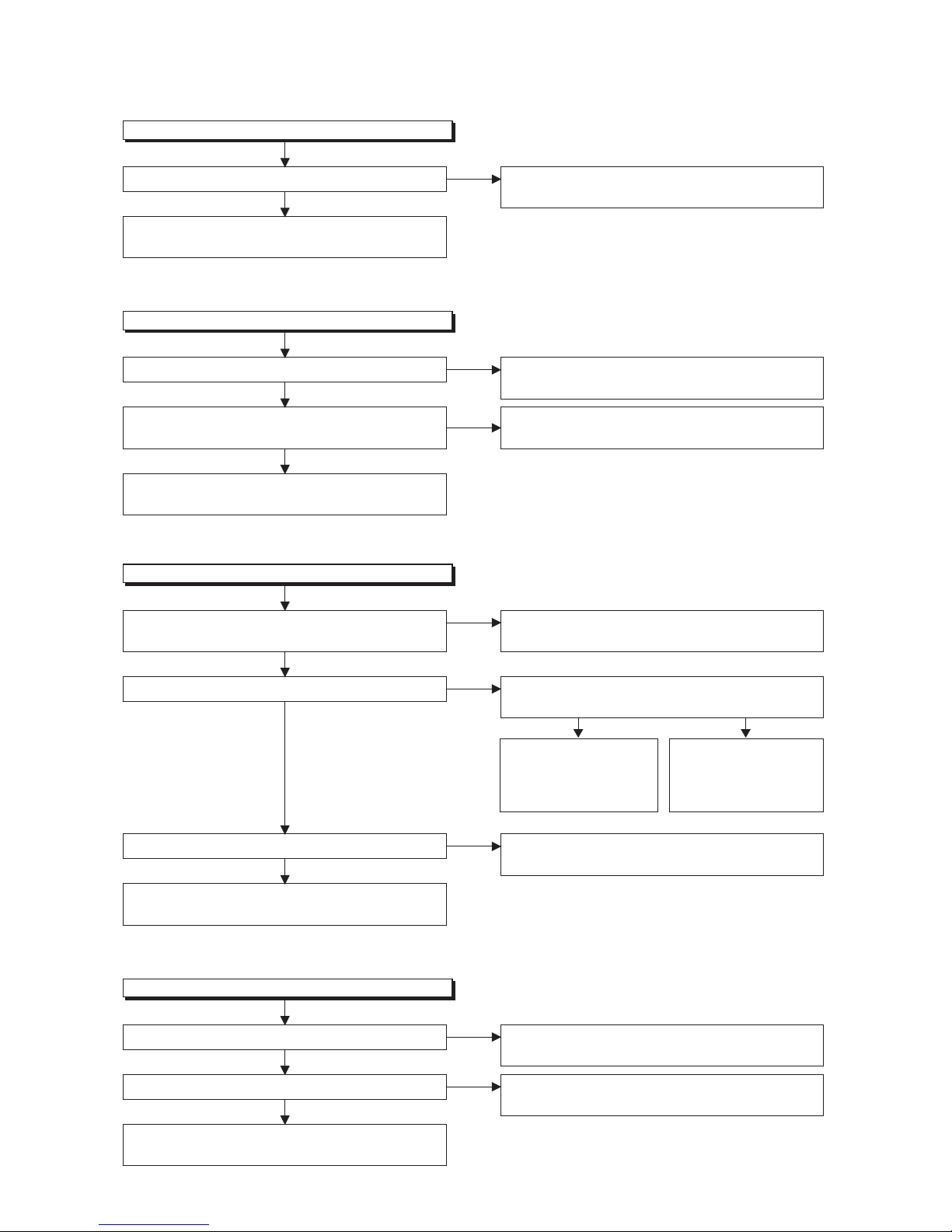
1-10-4 E9NG0TR
Ye s
Check for load circuit short-circuiting or leak, and
replace P1(AV ASSEMBLY) if defective.
Is the "H" pulse (approximately 6V) inputted to
the base of Q1106?
Refer to "FLOW CHART NO.16"<P-ON+10V is not
outputted>.
No
Ye s
Check Q1106 and their periphery, and
replace P3(PW/SW ASSEMBLY) if defective.
FLOW CHART NO.15
P-ON+5V(2) is not outputted.
Is the supply voltage 5V fed to the cathode of D016?
Check D016 and their periphery, and replace
P3(PW/SW ASSEMBLY) if defective.
No
Ye s
FLOW CHART NO.16
P-ON+10V is not outputted.
Is the supply voltage 14V fed to the cathode
of D1031?
Check D1031 and their periphery, and replace
P3(PW/SW ASSEMBLY) if defective.
No
Ye s
Ye s
No
Is 3.3V voltage outputted to pin 2 of IC1104?
FLOW CHART NO.17
P-ON+3.3V is not outputted.
Is the supply voltage 5V fed to the cathode of D1103?
Check D1103 and their periphery, and replace
P3(PW/SW ASSEMBLY) if defective.
No
Ye s
Check IC1104 and their periphery, and replace
P3(PW/SW ASSEMBLY) if defective.
No
FLOW CHART NO.14
ECO+9V is not outputted.
Is 10V voltage supplied to collector of Q1521?
Refer to "FLOW CHART NO.8"<AL+12V is not
outputted>.
No
Ye s
Check Q1521 and their periphery, and
replace P1(AV ASSEMBLY) if defective.
Is 10V voltage outputed to pin 12 of CL1001? Cheak Q1105 and their periphery, and replace
P3(PW/SW ASSEMBLY) if defective.
No
Ye s
Is 12V voltage supplied to collector of Q1105?
Check for load circuit short-circuiting or leak, and
replace P1(AV ASSEMBLY) if defective.
Is the "H" pulse (approximately 0.7V) inputted to
the base of Q1514?
Check Q1511, Q1514
and their periphety, and
replace P3(PW/SW
ASSEMBLY) if defective.
Ye s
Check the POW-SW
signal line, and replace
P1(AV ASSEMBLY)
if defective.
No
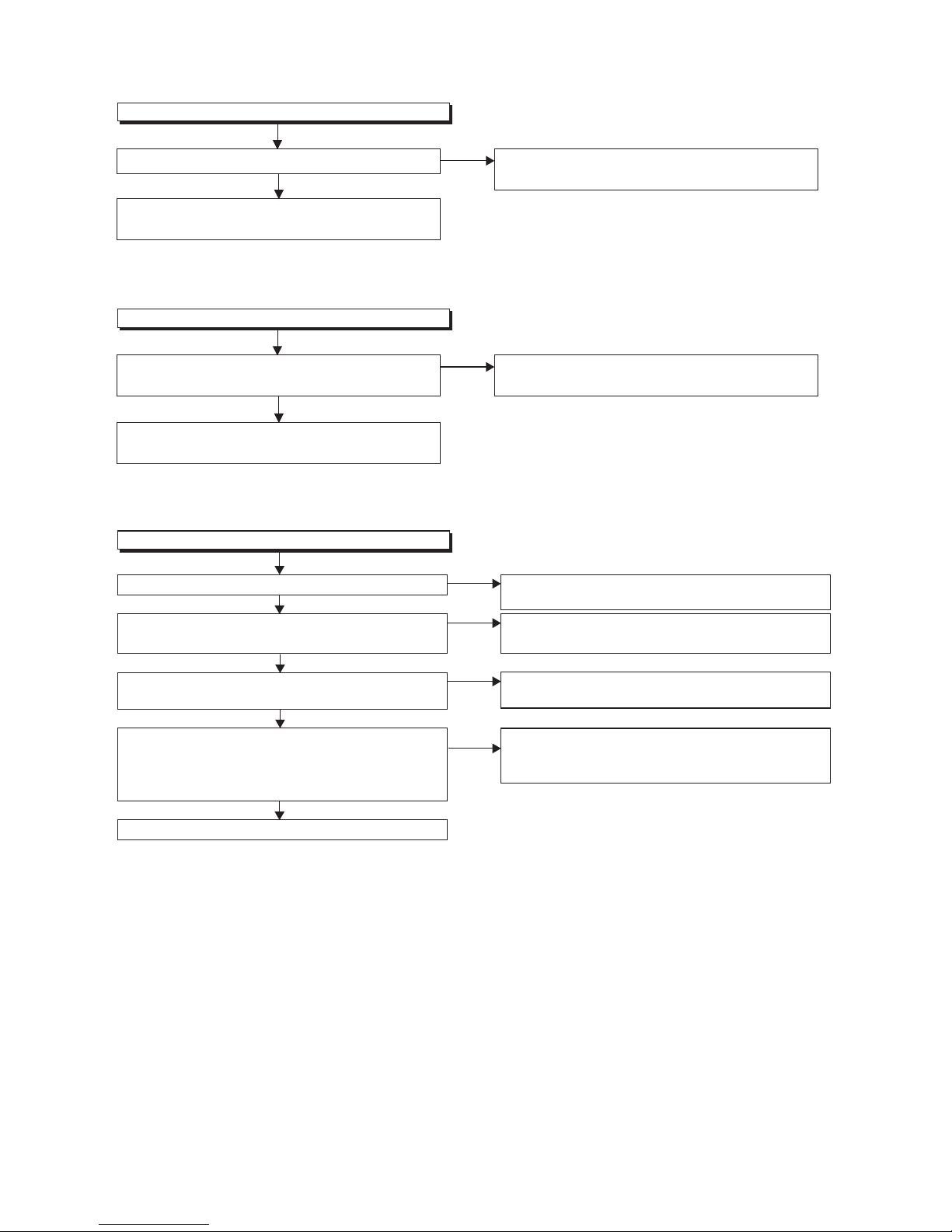
1-10-5 E9NG0TR
Ye s
Ye s
Ye s
Ye s
No
No
No
No
FLOW CHART NO.20
The fluorescent display tube does not light up.
Is 5V voltage supplied to Pin(13,43) of IC612?
Is approximately -24V to -28V voltage supplied to
Pin(30) of IC612?
Is there approximately 500kHz oscillation to
Pin(5) of IC612?
Are the filament voltage applied between Pin(1)
and Pin(24) of the fluorescent display tube?
Also negative voltage applied between these pins
and GND?
Replace P1(AV ASSEMBLY)
.
Check the ECO+5V line and replace
P1(AV ASSEMBLY) if defective.
Check the -FL line and replace P1(AV ASSEMBLY)
or P3(PW/SW ASSEMBLY) if defective.
Check R618, IC612 and their periphery, and
replace P1(AV ASSEMBLY) if defective.
Check the power circuit, D1103, D1108, R1106,
C1110 and their periphery, and replace
P3(PW/SW ASSEMBLY) if defective.
Check Q1527, Q1528 and their
periphery,
and
replace P1(AV ASSEMBLY) if defective.
FLOW CHART NO.18
SYS+5V is not outputted.
Is 5V voltage
supplied
to emitter of Q1527?
No
Ye s
Refer to "FLOW CHART NO.11"<AL+5V is not
outputted>.
Check IC1800 and their
periphery,
and replace
P1(AV ASSEMBLY) if defective.
FLOW CHART NO.19
P-ON+1.8V is not outputted.
Is the supply voltage 2.8V fed to the cathode
of D1030?
No
Ye s
Check D1030 and their periohery, and replace
P3(PW/SW ASSEMBLY) if defective.
1-10-6 E9NG0TR
2 DVD Section
0.51
0.92
1.27
1.61
1.98
2.39
2.90
3.60
4.30
OPEN
/CLOSE
DVD
-PLAY
DVD
DVD
-STOP
DVD
-REC
Terminal voltage of IC501-8
KEY-1
IC501-8
(V)
---
---
---
DUBBING
Ye s
No
FLOW CHART NO.1
The key operation is not functioning.
Are the contact point and the installation state of
the key switches normal?
Is the control voltage normally inputted into
Pin(8) of IC501?
Check the key switches and their periphery, and
replace P3(PW/SW ASSEMBLY) if defective.
No
Re-install the key switches correctly or replace
P3(PW/SW ASSEMBLY).
FLOW CHART NO.2
No DVD operation is possible from the remote control. (
Operation is possible from the unit.)
Replace P1(AV ASSEMBLY) or remote control(X1).
Check the line between the RS1501 (remote
control receiver) and Pin(14) of IC501, and replace
P1(AV ASSEMBLY) if defective.
Is the "L" pulse sent out from Pin(1) terminal of the
RS1501 (remote control receiver) when the remote
control is activated?
Is the "L" pulse signal supplied to Pin(14) of
IC501?
Replace P1(AV ASSEMBLY) or P2(DVD
MECHANISM & DVD MAIN BOARD ASSEMBLY).
Ye s
Ye s
Replace P1(AV ASSEMBLY) or P2(DVD
MECHANISM & DVD MAIN BOARD ASSEMBLY).
Ye s
Is 5V voltage supplied to Pin(3) terminal of the
RS1501 (remote control receiver)?
Ye s
No
Check AL+5V line, and replace P1(AV ASSEMBLY)
if defective.
No
No
FLOW CHART NO.3
Replace the P2(DVD MECHANISM & DVD MAIN
BOARD ASSEMBLY).
The [No Disc] indication.
Both picture and sound do not operate normally.
1-10-7 E9NG0TR
Are the video signals outputted to each pin of
CN1502?
Ye s
No
FLOW CHART NO.4
VIDEO E-E does not appear normally.
Are the video signals inputted to each pin of
IC1509?
Check the line between video input terminal and
each pin of IC1509, and replace P1(AV
ASSEMBLY), P5(BOARD DTV MODULE UNIT)
or TU1800.
Are the video signals outputted to each pin of
IC1509?
Ye s
Ye s
No
No
IC1509 VIDEO-IN 1 (AV1)18PIN
IC1509 VIDEO-IN (FRONT)14PIN
IC1509 DTV-Y3PIN
IC1509 VIDEO-Y/CVBS-IN61PIN
IC1509 VIDEO-C-IN59PIN
CN1502 VIDEO-Y/CVBS-IN20PIN
CN1502 VIDEO-C-IN22PIN
VIDEO-Y/CVBS-IN
20PIN
VIDEO-C-IN
22PIN
IC1509 DTV-C5PIN
IC1509 VIDEO-IN 2 (AV2)12PIN
IC1509 TUNER-VIDEO
VIDEO-IN 1 (AV1)
DTV-Y
DTV-C
VIDEO-IN 2 (AV2)
20PIN
IC1509
→ JK150418PIN
VIDEO-IN (FRONT)
IC1509
→ JK123114PIN
IC1509
→ CN1800 26PIN3PIN
IC1509
→ CN
1502
61PIN
IC1509
→ CN
1502
59PIN
Check the line between each pin of IC1509 and
each pin of CN1502 and replace P1(AV
ASSEMBLY) if defective.
IC1509
→ CN1800 28PIN5PIN
IC1509
→ JK200112PIN
TUNER-VIDEO
IC1509
→ TU1800 17PIN20PIN
Continued to A on the next page.
Check the ECO+5V, ECO+9V
line and replace P1(AV
ASSEMBLY) or P3(PW/SW
ASSEMBLY) if defective.
Replace P1(AV
ASSEMBLY).
Ye s N o
Is 5V voltage supplied to Pin(27,29,47,63) of
IC1509?
Is 9V voltage supplied to Pin(75) of IC1509?
1-10-8 E9NG0TR
Are the video signals outputted to each pin of
IC1509?
Ye s
Ye s
No
Check the periphery of JK1504 from Pin (30) of IC1509
and replace P1(AV ASSEMBLY) if defective.
Check the periphery of JK2001 from Pin (22) of IC1509
and replace P1(AV ASSEMBLY) if defective.
Check the periphery of JK1505 from Pin (38, 39, 40) of
IC1509 and replace P1(AV ASSEMBLY) if defective.
Are the video signals outputted to the specific
output terminal?
No
No
No
Are the composite video signals outputted to
the VIDEO OUT (AV1) terminal (JK1504)?
Are the composite video signals outputted to
the VIDEO OUT (AV2) terminal (JK2001)?
Are the component video signals outputted to
the VIDEO OUT terminal (JK1505)?
Are the video signals outputted to each pin of
CN1502?
Replace the P2(DVD MECHANISM & DVD MAIN
BOARD ASSEMBLY).
Check the line between each pin of CN1502 and
each pin of IC1509, and replace P1(AV
ASSEMBLY) if defective.
Are the video signals shown above inputted into
each pin of IC1509?
Ye s
No
No
CN1502 VIDEO-Y(I/P)-OUT7PIN
CN1502 VIDEO-Y(I)-OUT1PIN
CN1502 VIDEO-Pr/Cr-OUT5PIN
CN1502 VIDEO-Pb/Cb-OUT3PIN
CN1502 VIDEO-C-OUT
VIDEO-Y(I/P)-OUT
VIDEO-
Pr/Cr
-OUT
VIDEO-
Pb/Cb
-OUT
VIDEO-C-OUT
9PIN
IC1509 VIDEO-Y(I/P)-OUT51PIN
IC1509 VIDEO-Y(I)-OUT55PIN
IC1509 VIDEO-Pr/Cr-OUT52PIN
IC1509 VIDEO-Pb/Cb-OUT53PIN
IC1509 VIDEO-C-OUT57PIN
IC1509 VIDEO-OUT 1 (AV1)30PIN
IC1509 VIDEO-OUT 2 (AV2)22PIN
IC1509 VIDEO-Y40PIN
IC1509 VIDEO-Pr/Cr39PIN
IC1509 VIDEO-Pb/Cb38PIN
CN1502 → IC15097PIN
CN1502 → IC15095PIN
CN1502 → IC15093PIN
→ IC1509
9PIN
51PIN
VIDEO-Y(I)-OUTCN1502 → IC15091PIN 55PIN
52PIN
53PIN
57PINCN1502
A
Check the ECO+5V, ECO+9V
line and replace P1(AV
ASSEMBLY) or P3(PW/SW
ASSEMBLY) if defective.
Replace P1(AV
ASSEMBLY).
Ye s N o
Is 5V voltage supplied to Pin(27,29,47,63) of
IC1509?
Is 9V voltage supplied to Pin(75) of IC1509?
1-10-9 E9NG0TR
FLOW CHART NO.5
Picture does not appear normally.
Set the disc on the disc tray, and playback it.
(DVD MODE)
Are the video signals outputted to each pin of
IC1509?
Ye s
Ye s
No
Check the periphery of JK1504 from Pin (30) of IC1509
and replace P1(AV ASSEMBLY) if defective.
Check the periphery of JK2001 from Pin (22) of IC1509
and replace P1(AV ASSEMBLY) if defective.
Check the periphery of JK1505 from Pin (38, 39, 40) of
IC1509 and replace P1(AV ASSEMBLY) if efective.
Are the video signals outputted to the specific
output terminal?
No
No
No
Are the composite video signals outputted to
the VIDEO OUT (AV1) terminal (JK1504)?
Are the composite video signals outputted to
the VIDEO OUT (AV2) terminal (JK2001)?
Are the component video signals outputted to
the VIDEO OUT terminal (JK1505)?
Are the video signals outputted to each pin of
CN1502?
Replace the P2(DVD MECHANISM & DVD MAIN
BOARD ASSEMBLY).
Check the line between each pin of CN1502 and
each pin of IC1509, and replace P1(AV
ASSEMBLY) if defective.
Are the video signals shown above inputted into
each pin of IC1509?
Ye s
No
No
CN1502 VIDEO-Y(I/P)-OUT7PIN
CN1502 VIDEO-Y(I)-OUT1PIN
CN1502 VIDEO-Pr/Cr-OUT5PIN
CN1502 VIDEO-Pb/Cb-OUT3PIN
CN1502 VIDEO-C-OUT
VIDEO-Y(I/P)-OUT
VIDEO-
Pr/Cr
-OUT
VIDEO-
Pb/Cb
-OUT
VIDEO-C-OUT
9PIN
IC1509 VIDEO-Y(I/P)-OUT51PIN
IC1509 VIDEO-Y(I)-OUT55PIN
IC1509 VIDEO-Pr/Cr-OUT52PIN
IC1509 VIDEO-Pb/Cb-OUT53PIN
IC1509 VIDEO-C-OUT57PIN
IC1509 VIDEO-OUT 1 (AV1)30PIN
IC1509 VIDEO-OUT 2 (AV2)22PIN
IC1509 VIDEO-Y40PIN
IC1509 VIDEO-Pr/Cr39PIN
IC1509 VIDEO-Pb/Cb38PIN
CN1502 → IC15097PIN
CN1502 → IC15095PIN
CN1502 → IC15093PIN
→ IC1509
9PIN
51PIN
VIDEO-Y(I)-OUTCN1502 → IC15091PIN 55PIN
52PIN
53PIN
57PINCN1502
Check the ECO+5V, ECO+9V
line and replace P1(AV
ASSEMBLY) or P3(PW/SW
ASSEMBLY) if defective.
Replace P1(AV
ASSEMBLY).
Ye s N o
Is 5V voltage supplied to Pin(27,29,47,63) of
IC1509?
Is 9V voltage supplied to Pin(75) of IC1509?
 Loading...