

Page 1

SERVICE MANUAL
DVD Video Recorder
FILE NO. 810-200617GR
®
D-R160SB
The above model is classified as a green product (*1), as indicated by the underlined serial
number. This Service Manual describes replacement parts for the green product. When
repairing this green product, use the part(s) described in this manual and lead-free solder (*2).
For (*1) and (*2), see the next page.
TOSHIBA CORPORATION 2006
Published in Japan, Mar. 2006 GREEN
Page 2

(*1) GREEN PRODUCT PROCUREMENT
The EC is actively promoting the WEEE & RoHS Directives that define standards for recycling
and reuse of Waste Electrical and Electronic Equipment and for the Restriction of the use of
certain Hazardous Substances. From July 1, 2006, the RoHS Directive will prohibit any
marketing of new products containing the restricted substances.
Increasing attention is given to issues related to the global environmental. Toshiba Corporation
recognizes environmental protection as a key management tasks, and is doing its utmost to
enhance and improve the quality and scope of its environmental activities. In line with this,
Toshiba proactively promotes Green Procurement, and seeks to purchase and use products,
parts and materials that have low environmental impacts.
Green procurement of parts is not only confined to manufacture. The same green parts used in
manufacture must also be used as replacement parts.
(*2) LEAD-FREE SOLDER
This product is manufactured using lead-free solder as a part of a movement within the consumer
products industry at large to be environmentally responsible. Lead-free solder must be used in the
servicing and repair of this product.
WARNING
This product is manufactured using lead free solder.
DO NOT USE LEAD BASED SOLDER TO REPAIR THIS PRODUCT !
The melting temperature of lead-free solder is higher than that of leaded solder by 86°F to 104°F
(30°C to 40°C). Use of a soldering iron designed for lead-based solders to repair product made
with lead-free solder may result in damage to the component and or BOARD being soldered.
Great care should be made to ensure high-quality soldering when servicing this product —
especially when soldering large components, through-hole pins, and on BOARDs — as the level
of heat required to melt lead-free solder is high.
Page 3

IMPORTANT SAFETY NOTICE
Proper service and repair is important to the safe, reliable operation of all
TOSHIBA Equipment. The service procedures recommended by TOSHIBA
and described in this service manual are effective methods of performing
service operations. Some of these service special tools should be used
when and as recommended.
It is important to note that this service manual contains various CAUTIONS
and NOTICES which should be carefully read in order to minimize the risk
of personal injury to service personnel. The possibility exists that improper
service methods may damage the equipment. It also is important to
understand that these CAUTIONS and NOTICES ARE NOT EXHAUSTIVE.
TOSHIBA could not possibly know, evaluate and advice the service trade of
all conceivable ways in which service might be done or of the possible
hazardous consequences of each way. Consequently, TOSHIBA has not
undertaken any such broad evaluation. Accordingly, a servicer who uses a
service procedure or tool which is not recommended by TOSHIBA must
first use all precautions thoroughly so that neither his safety nor the safe
operation of the equipment will be jeopardized by the service method
selected.
TABLE OF CONTENTS
Specifications . . . . . . . . . . . . . . . . . . . . . . . . . . . . . . . . . . . . . . . . . . . . . . . . . . . . . . . . . . . . . . . . . . . . . . . . . . 1-1-1
Laser Beam Safety Precautions. . . . . . . . . . . . . . . . . . . . . . . . . . . . . . . . . . . . . . . . . . . . . . . . . . . . . . . . . . . . 1-2-1
Important Safety Precautions. . . . . . . . . . . . . . . . . . . . . . . . . . . . . . . . . . . . . . . . . . . . . . . . . . . . . . . . . . . . . . 1-3-1
Standard Notes for Servicing . . . . . . . . . . . . . . . . . . . . . . . . . . . . . . . . . . . . . . . . . . . . . . . . . . . . . . . . . . . . . . 1-4-1
Cabinet Disassembly Instructions . . . . . . . . . . . . . . . . . . . . . . . . . . . . . . . . . . . . . . . . . . . . . . . . . . . . . . . . . . 1-5-1
How to Initialize the DVD Recorder . . . . . . . . . . . . . . . . . . . . . . . . . . . . . . . . . . . . . . . . . . . . . . . . . . . . . . . . . 1-6-1
Firmware Renewal Mode . . . . . . . . . . . . . . . . . . . . . . . . . . . . . . . . . . . . . . . . . . . . . . . . . . . . . . . . . . . . . . . . . 1-7-1
Troubleshooting . . . . . . . . . . . . . . . . . . . . . . . . . . . . . . . . . . . . . . . . . . . . . . . . . . . . . . . . . . . . . . . . . . . . . . . . 1-8-1
Function Indicator Symbols . . . . . . . . . . . . . . . . . . . . . . . . . . . . . . . . . . . . . . . . . . . . . . . . . . . . . . . . . . . . . . . 1-9-1
Block Diagrams . . . . . . . . . . . . . . . . . . . . . . . . . . . . . . . . . . . . . . . . . . . . . . . . . . . . . . . . . . . . . . . . . . . . . . . 1-10-1
Schematic Diagrams / BOARD’s and Test Points . . . . . . . . . . . . . . . . . . . . . . . . . . . . . . . . . . . . . . . . . . . . . 1-11-1
Waveforms . . . . . . . . . . . . . . . . . . . . . . . . . . . . . . . . . . . . . . . . . . . . . . . . . . . . . . . . . . . . . . . . . . . . . . . . . . . 1-12-1
Wiring Diagram . . . . . . . . . . . . . . . . . . . . . . . . . . . . . . . . . . . . . . . . . . . . . . . . . . . . . . . . . . . . . . . . . . . . . . . 1-13-1
System Control Timing Charts . . . . . . . . . . . . . . . . . . . . . . . . . . . . . . . . . . . . . . . . . . . . . . . . . . . . . . . . . . . . 1-14-1
IC Pin Function Descriptions . . . . . . . . . . . . . . . . . . . . . . . . . . . . . . . . . . . . . . . . . . . . . . . . . . . . . . . . . . . . . 1-15-1
Lead Identifications . . . . . . . . . . . . . . . . . . . . . . . . . . . . . . . . . . . . . . . . . . . . . . . . . . . . . . . . . . . . . . . . . . . . 1-16-1
Exploded Views . . . . . . . . . . . . . . . . . . . . . . . . . . . . . . . . . . . . . . . . . . . . . . . . . . . . . . . . . . . . . . . . . . . . . . . 1-17-1
Mechanical Parts List . . . . . . . . . . . . . . . . . . . . . . . . . . . . . . . . . . . . . . . . . . . . . . . . . . . . . . . . . . . . . . . . . . . 1-18-1
Electrical Parts List . . . . . . . . . . . . . . . . . . . . . . . . . . . . . . . . . . . . . . . . . . . . . . . . . . . . . . . . . . . . . . . . . . . . 1-19-1
Manufactured under license from Dolby Laboratories.
“Dolby” and the double-D symbol are trademarks of Dolby Laboratories.
Page 4

SPECIFICATIONS
General
System
DVD-Video, DVD-R/RW, CD-DA, CD-R/RW,
VCD, SVCD
Power requirements
220–240V
Power consumption
25W (standby: 4.5W)
Weight
2.4kg
Dimensions (width x height x depth)
435 x 66 x 244mm
Operating temperature
5ºC to 40ºC
Operating humidity
Less than 80% (no condensation)
TV format
PAL - I
± 10%, 50Hz ± 0.5%
Recording
Recording format
Video Recording format (DVD-RW only),
Video format (DVD-RW, DVD-R)
Recordable discs
DVD-Rewritable, DVD-Recordable
Video recording format
Sampling frequency : 13.5MHz
Compression format : MPEG
Audio recording format
Sampling frequency : 48kHz
Compression format : Dolby Digital
Tuner
Receivable channels
IRA - E69
Input/Output
Front Panel : (AV4)
Video input
One RCA connector
Input level : 1Vp-p (75 Ω)
S-Video input
One Mini DIN 4-pin jack
Input level : Y (Iuminance) 1Vp-p (75 Ω)
C (colour) 300mVp-p (75 Ω)
Audio input
Two RCA connectors
Input level : 2Vrms (Input impedance: more than
10kΩ)
Rear Panel :
VHF/UHF antenna input/output terminal
VHF/UHF set 75 Ω
Audio input /output
Two 21-pin scart jack (AV1, AV2)
Video input /output
Two 21-pin scart jack (AV1, AV2)
Input /output level : 1Vp-p (75 Ω) each
S-Video input (AV3) /output
Two Mini DIN 4-pin jacks
Input /output level :
Y (Iuminance) 1Vp-p (75 Ω)
C (colour) 300mVp-p (75 Ω)
Component video output
Three RCA connectors
Output level : Y: 1.0Vp-p (75 Ω)
P
Audio input
Two RCA connectors (AV3)
Input level : 2Vrms (Input impedance: more than
Analogue audio output
Two RCA connectors
Output level : 2Vrms (Output impedance:
Digital audio output
One Coaxial pin jack
Output level : 500mVp-p (75 Ω)
B /CB , P R /CR : 0.7Vp-p (75 Ω) each
10kΩ)
680
Ω)
Note
The specifications and design of this product are subject to
change without notice.
1-1-1 E7B71SP
Page 5
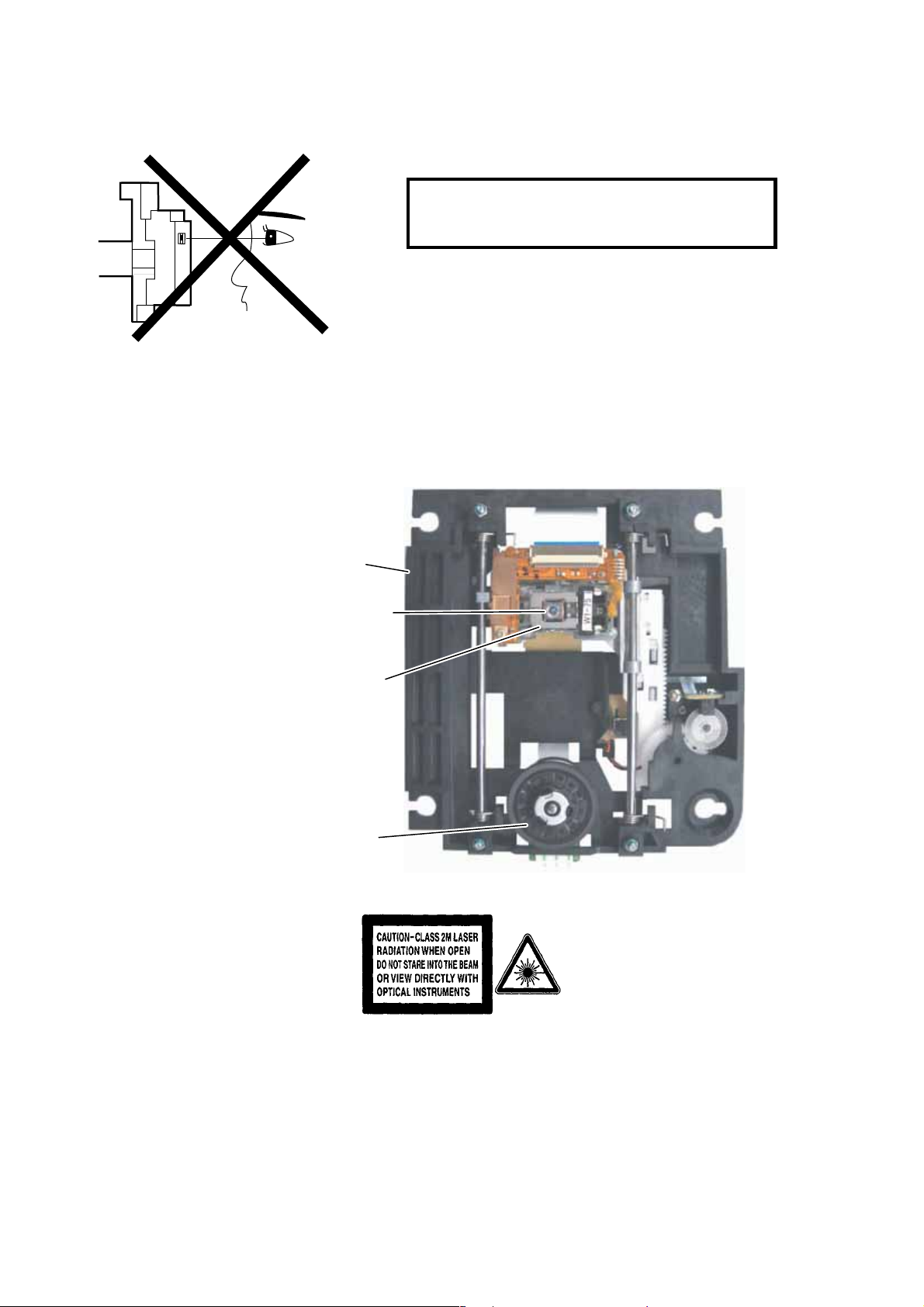
LASER BEAM SAFETY PRECAUTIONS
This DVD player uses a pickup that emits a laser beam.
Do not look directly at the laser beam coming
from the pickup or allow it to strike against your
skin.
The laser beam is emitted from the location shown in the figure. When checking the laser diode, be sure to keep
your eyes at least 30 cm away from the pickup lens when the diode is turned on. Do not look directly at the laser
beam.
CAUTION: Use of controls and adjustments, or doing procedures other than those specified herein, may result in
hazardous radiation exposure.
Drive Mechanism Assembly
Laser Beam Radiation
Laser Pickup
Turntable
Location: Inside Top of DVD mechanism.
1-2-1 R3PLSP
Page 6

IMPORTANT SAFETY PRECAUTIONS
Product Safety Notice
Some electrical and mechanical parts have special
safety-related characteristics which are often not evident from visual inspection, nor can the protection
they give necessarily be obtained by replacing them
with components rated for higher voltage, wattage,
etc. Parts that have special safety characteristics are
identified by a ! on schematics and in parts lists. Use
of a substitute replacement that does not have the
same safety characteristics as the recommended
replacement part might create shock, fire, and/or other
hazards. The Product’s Safety is under review continuously and new instructions are issued whenever
appropriate. Prior to shipment from the factory, our
products are carefully inspected to confirm with the
recognized product safety and electrical codes of the
countries in which they are to be sold. However, in
order to maintain such compliance, it is equally important to implement the following precautions when a set
is being serviced.
Precautions during Servicing
A. Parts identified by the ! symbol are critical for
safety. Replace only with part number specified.
B. In addition to safety, other parts and assemblies
are specified for conformance with regulations
applying to spurious radiation. These must also be
replaced only with specified replacements.
Examples: RF converters, RF cables, noise blocking capacitors, and noise blocking filters, etc.
C. Use specified internal wiring. Note especially:
1)Wires covered with PVC tubing
2)Double insulated wires
3)High voltage leads
D. Use specified insulating materials for hazardous
live parts. Note especially:
1)Insulation tape
2)PVC tubing
3)Spacers
4)Insulators for transistors
E. When replacing AC primary side components
(transformers, power cord, etc.), wrap ends of
wires securely about the terminals before soldering.
F. Observe that the wires do not contact heat produc-
ing parts (heatsinks, oxide metal film resistors, fusible resistors, etc.).
G. Check that replaced wires do not contact sharp
edges or pointed parts.
H. When a power cord has been replaced, check that
5 - 6 kg of force in any direction will not loosen it.
I. Also check areas surrounding repaired locations.
J. Be careful that foreign objects (screws, solder
droplets, etc.) do not remain inside the set.
K. Crimp type wire connector
The power transformer uses crimp type connectors
which connect the power cord and the primary side
of the transformer. When replacing the transformer,
follow these steps carefully and precisely to prevent shock hazards.
Replacement procedure
1)Remove the old connector by cutting the wires at a
point close to the connector.
Important: Do not re-use a connector. (Discard it.)
2)Strip about 15 mm of the insulation from the ends
of the wires. If the wires are stranded, twist the
strands to avoid frayed conductors.
3)Align the lengths of the wires to be connected.
Insert the wires fully into the connector.
4)Use a crimping tool to crimp the metal sleeve at its
center. Be sure to crimp fully to the complete closure of the tool.
L. When connecting or disconnecting the internal
connectors, first, disconnect the AC plug from the
AC outlet.
1-3-1 DVD_SFNP
Page 7
Safety Check after Servicing
Examine the area surrounding the repaired location
for damage or deterioration. Observe that screws,
parts, and wires have been returned to their original
positions. Afterwards, do the following tests and confirm the specified values to verify compliance with
safety standards.
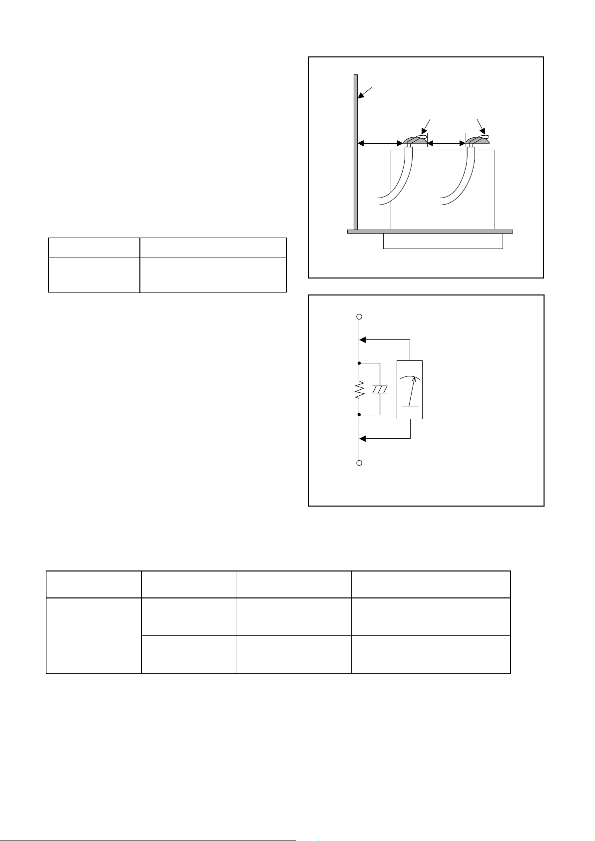
1. Clearance Distance
When replacing primary circuit components, confirm
specified clearance distance (d) and (d’) between soldered terminals, and between terminals and surrounding metallic parts. (See Fig. 1)
Table 1 : Ratings for selected area
AC Line Voltage Clearance Distance (d), (d’)
Chassis or Secondary Conductor
Primary Circuit
d' d
220 to 240 V
Note: This table is unofficial and for reference only.
Be sure to confirm the precise values.
≥ 3 mm(d)
≥ 6 mm(d’)
2. Leakage Current Test
Confirm the specified (or lower) leakage current
between B (earth ground, power cord plug prongs)
and externally exposed accessible parts (RF terminals, antenna terminals, video and audio input and
output terminals, microphone jacks, earphone jacks,
etc.) is lower than or equal to the specified value in the
table below.
Measuring Method (Power ON) :
Insert load Z between B (earth ground, power cord
plug prongs) and exposed accessible parts. Use an
AC voltmeter to measure across the terminals of load
Z. See Fig. 2 and the following table.
Exposed Accessible Part
Z
One side of
B
Power Cord Plug Prongs
Fig. 1
AC Voltmeter
(High Impedance)
Fig. 2
Table 2: Leakage current ratings for selected areas
AC Line Voltage Load Z Leakage Current (i)
2kΩ RES.
Connected in
220 to 240 V
Note: This table is unofficial and for reference only. Be sure to confirm the precise values.
parallel
50kΩ RES.
Connected in
parallel
i≤0.7mA AC Peak
i≤2mA DC
i≤0.7mA AC Peak
i≤2mA DC
1-3-2 DVD_SFNP
One side of power cord plug
prongs (B) to:
RF or
Antenna terminals
A/V Input, Output
Page 8
STANDARD NOTES FOR SERVICING
NOTE: BOARD MEANS PRINTED CIRCUIT BOARD.
Circuit Board Indications
1. The output pin of the 3 pin Regulator ICs is
indicated as shown.
Top View
Out
2. For other ICs, pin 1 and every fifth pin are
indicated as shown.
Pin 1
3. The 1st pin of every male connector is indicated as
shown.
Pin 1
Input
In
Bottom View
5
10
Pb (Lead) Free Solder
When soldering, be sure to use the Pb free solder.
How to Remove / Install Flat Pack-IC
1. Removal
With Hot-Air Flat Pack-IC Desoldering Machine:
1. Prepare the hot-air flat pack-IC desoldering
machine, then apply hot air to the Flat Pack-IC
(about 5 to 6 seconds). (Fig. S-1-1)
Fig. S-1-1
Instructions for Connectors
1. When you connect or disconnect the FFC (Flexible
Foil Connector) cable, be sure to first disconnect
the AC cord.
2. FFC (Flexible Foil Connector) cable should be
inserted parallel into the connector, not at an
angle.
FFC Cable
Connector
BOARD
* Be careful to avoid a short circuit.
2. Remove the flat pack-IC with tweezers while
applying the hot air.
3. Bottom of the flat pack-IC is fixed with glue to the
BOARD; when removing entire flat pack-IC, first
apply soldering iron to center of the flat pack-IC
and heat up. Then remove (glue will be melted).
(Fig. S-1-6)
4. Release the flat pack-IC from the BOARD using
tweezers. (Fig. S-1-6)
CAUTION:
1. The Flat Pack-IC shape may differ by models. Use
an appropriate hot-air flat pack-IC desoldering
machine, whose shape matches that of the Flat
Pack-IC.
2. Do not supply hot air to the chip parts around the
flat pack-IC for over 6 seconds because damage
to the chip parts may occur. Put masking tape
around the flat pack-IC to protect other parts from
damage. (Fig. S-1-2)
1-4-1 DVDN_SN
Page 9
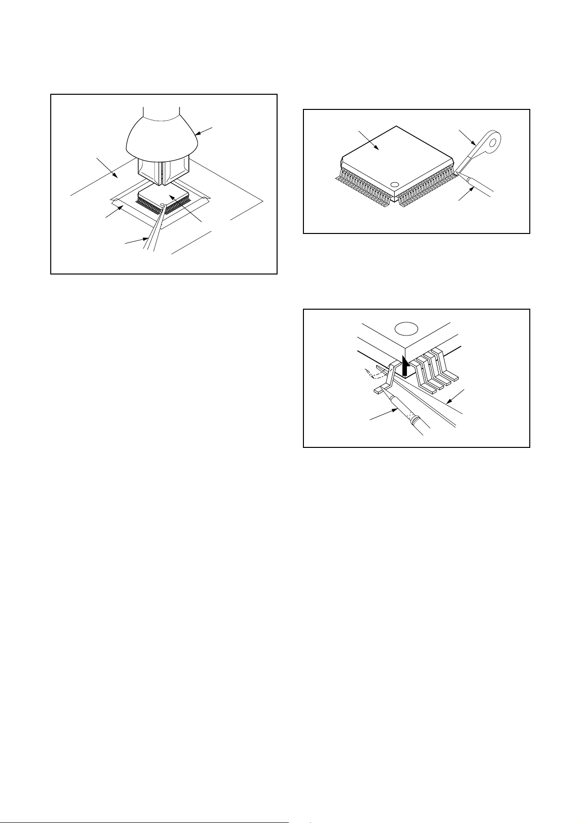
3. The flat pack-IC on the BOARD is affixed with
glue, so be careful not to break or damage the foil
of each pin or the solder lands under the IC when
removing it.
With Soldering Iron:
1. Using desoldering braid, remove the solder from
all pins of the flat pack-IC. When you use solder
flux which is applied to all pins of the flat pack-IC,
you can remove it easily. (Fig. S-1-3)
BOARD
Masking
Tape
Tweezers
Hot-air
Flat Pack-IC
Desoldering
Machine
Flat Pack-IC
Fig. S-1-2
Flat Pack-IC
Desoldering Braid
Soldering Iron
Fig. S-1-3
2. Lift each lead of the flat pack-IC upward one by
one, using a sharp pin or wire to which solder will
not adhere (iron wire). When heating the pins, use
a fine tip soldering iron or a hot air desoldering
machine. (Fig. S-1-4)
Sharp
Pin
Fine Tip
Soldering Iron
3. Bottom of the flat pack-IC is fixed with glue to the
BOARD; when removing entire flat pack-IC, first
apply soldering iron to center of the flat pack-IC
and heat up. Then remove (glue will be melted).
(Fig. S-1-6)
4. Release the flat pack-IC from the BOARD using
tweezers. (Fig. S-1-6)
Fig. S-1-4
1-4-2 DVDN_SN
Page 10
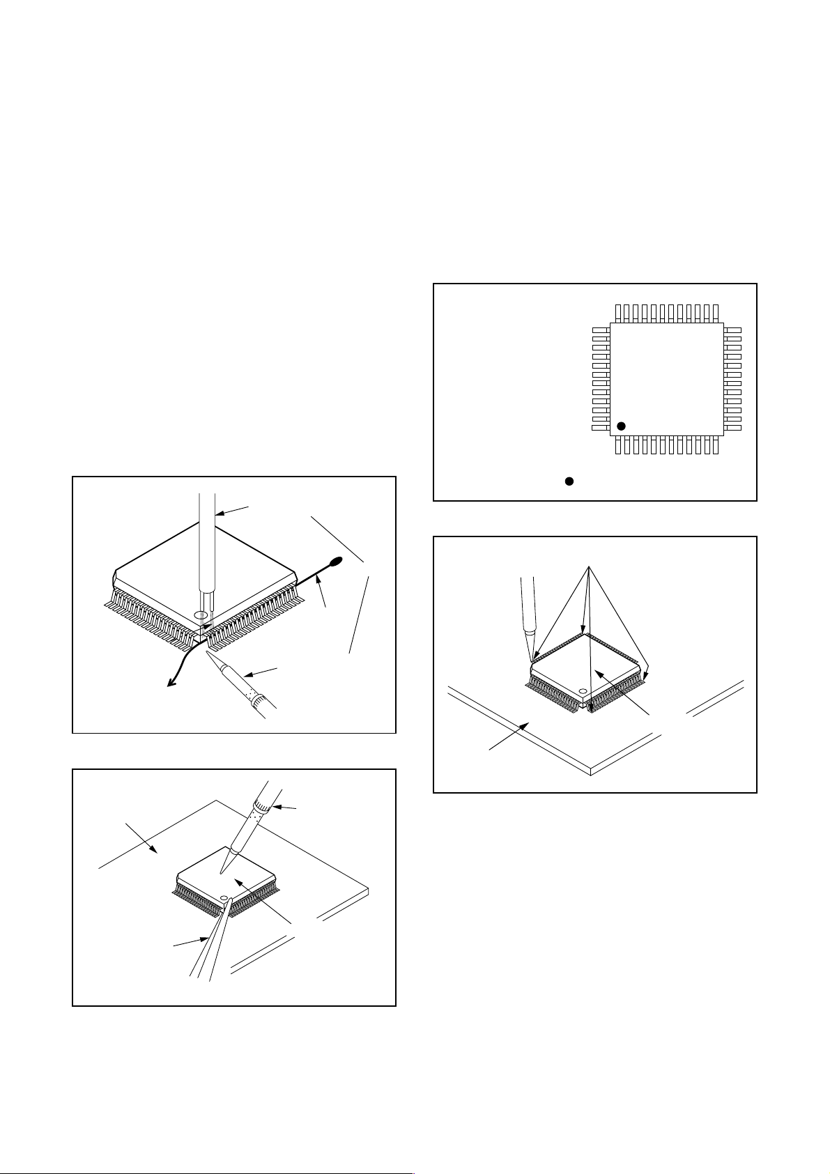
With Iron Wire:
1. Using desoldering braid, remove the solder from
all pins of the flat pack-IC. When you use solder
flux which is applied to all pins of the flat pack-IC,
you can remove it easily. (Fig. S-1-3)
2. Affix the wire to a workbench or solid mounting
point, as shown in Fig. S-1-5.
3. While heating the pins using a fine tip soldering
iron or hot air blower, pull up the wire as the solder
melts so as to lift the IC leads from the BOARD
contact pads as shown in Fig. S-1-5.
4. Bottom of the flat pack-IC is fixed with glue to the
BOARD; when removing entire flat pack-IC, first
apply soldering iron to center of the flat pack-IC
and heat up. Then remove (glue will be melted).
(Fig. S-1-6)
5. Release the flat pack-IC from the BOARD using
tweezers. (Fig. S-1-6)
Note: When using a soldering iron, care must be
taken to ensure that the flat pack-IC is not
being held by glue. When the flat pack-IC is
removed from the BOARD, handle it gently
because it may be damaged if force is applied.
Hot Air Blower
2. Installation
1. Using desoldering braid, remove the solder from
the foil of each pin of the flat pack-IC on the
BOARD so you can install a replacement flat packIC more easily.
2. The “●” mark on the flat pack-IC indicates pin 1.
(See Fig. S-1-7.) Be sure this mark matches the 1
on the BOARD when positioning for installation.
Then presolder the four corners of the flat pack-IC.
(See Fig. S-1-8.)
3. Solder all pins of the flat pack-IC. Be sure that
none of the pins have solder bridges.
Example :
Pin 1 of the Flat Pack-IC
is indicated by a " " mark.
Fig. S-1-7
To Solid
Mounting Point
BOARD
Tweezers
Iron Wire
Soldering Iron
Fig. S-1-5
Fine Tip
Soldering Iron
Flat Pack-IC
or
Presolder
Flat Pack-IC
BOARD
Fig. S-1-8
Fig. S-1-6
1-4-3 DVDN_SN
Page 11
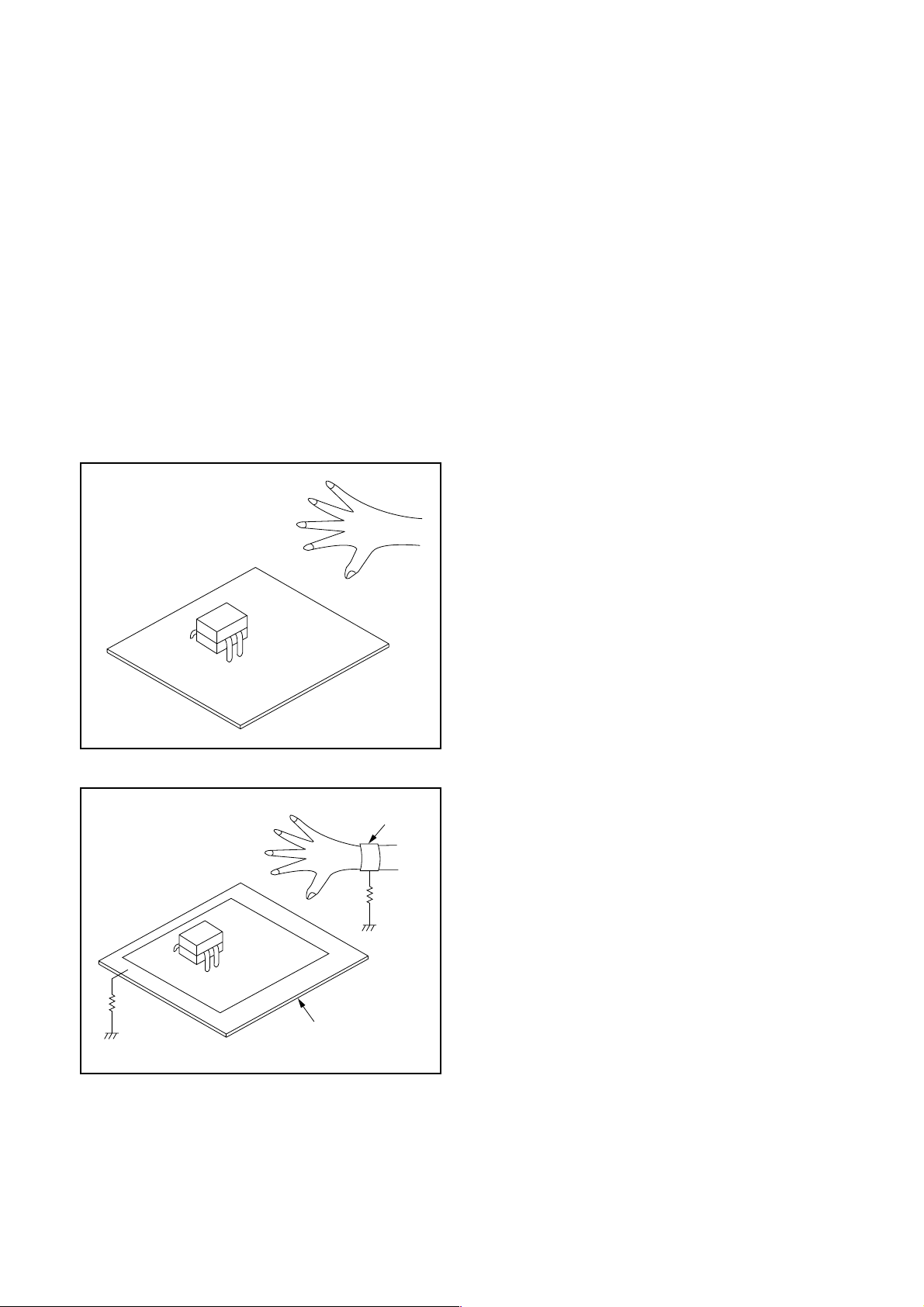
Instructions for Handling Semiconductors
Electrostatic breakdown of the semi-conductors may
occur due to a potential difference caused by
electrostatic charge during unpacking or repair work.
1. Ground for Human Body
Be sure to wear a grounding band (1 MΩ) that is
properly grounded to remove any static electricity that
may be charged on the body.
2. Ground for Workbench
Be sure to place a conductive sheet or copper plate
with proper grounding (1 MΩ) on the workbench or
other surface, where the semi-conductors are to be
placed. Because the static electricity charge on
clothing will not escape through the body grounding
band, be careful to avoid contacting semi-conductors
with your clothing.
<Incorrect>
<Correct>
1MΩ
BOARD
Grounding Band
1MΩ
BOARD
Conductive Sheet or
Copper Plate
1-4-4 DVDN_SN
Page 12
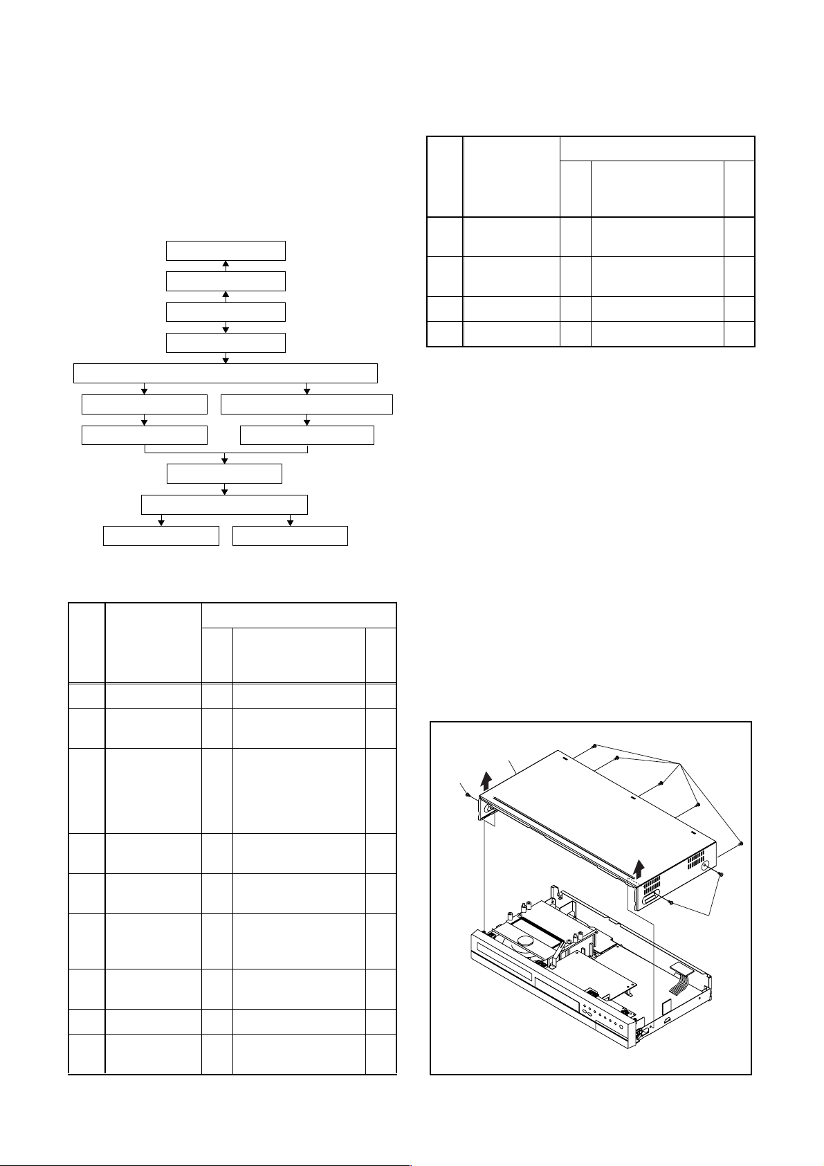
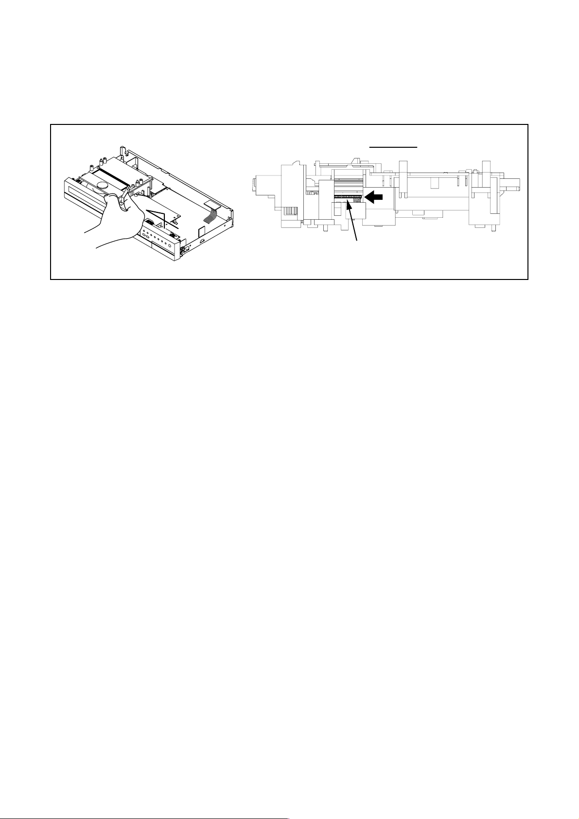
CABINET DISASSEMBLY INSTRUCTIONS
NOTE: BOARD MEANS PRINTED CIRCUIT BOARD.
1. Disassembly Flowchart
This flowchart indicates the disassembly steps to gain
access to item(s) to be serviced. When reassembling,
follow the steps in reverse order. Bend, route, and
dress the cables as they were originally.
[9] FAN
[8] FAN COVER
[1] COVER TOP
[2] PANEL FRONT
[3] DVD MECHANISM & DVD MAIN BOARD ASSEMBLY
[4] BOARD SWITCH
[5] BOARD HOLDER
[10] PANEL REAR
[11] BOARD POWER
[12] BOARD JACK [13] BOARD AFV
[6]
BOARD POWER SUPPLY
[7] POWER HOLDER
2. Disassembly Method
ID/
Loc.
No.
Part
Fig.
No.
[1] COVER TOP D1 8(S-1) ---
Removal
Remove/*Unhook/
Unlock/Release/
Unplug/Desolder
Note
ID/
Removal
Loc.
Part
No.
[10] PANEL REAR D5
BOARD
[11]
POWER
Remove/*Unhook/
Fig.
Unlock/Release/
No.
Unplug/Desolder
Note
(S-8), 6(S-9),
2(S-10)
D6 3(S-11) ---
---
[12] BOARD JACK D6 Desolder ---
[13] BOARD AFV D6 Desolder ---
↓
(1)
↓
(2)
↓
(3)
↓
(4)
(5)
Note:
(1) Identification (location) No. of parts in the figures
(2) Name of the part
(3) Figure Number for reference
(4) Identification of parts to be removed, unhooked,
unlocked, released, unplugged, unclamped, or
desoldered.
P = Spring, L = Locking Tab, S = Screw,
CN = Connector
* = Unhook, Unlock, Release, Unplug, or Desolder
e.g. 2(S-2) = two Screws (S-2),
2(L-2) = two Locking Tabs (L-2)
(5) Refer to “Reference Notes.”
Reference Notes
1. CAUTION 1: Locking Tabs (L-1) and (L-2) are
fragile. Be careful not to break them.
↓
PA NE L
[2]
FRONT
D2 *6(L-1), *3(L-2) 1
DVD
MECHANISM
& DVD MAIN
[3]
BOARD
4(S-2), *CN101,
D3
*CN701, LOCKING
CARD SPACERS
---
ASSEMBLY
BOARD
[4]
[5]
SWITCH
BOARD
HOLDER
D4 (S-3), Desolder ---
D4 2(S-4) ---
BOARD
[6]
POWER
D4 2(S-5), *CN1152 ---
SUPPLY
POWER
[7]
HOLDER
D4 (S-6) ---
[8] FAN COVER D5 2(S-7) ---
[9] FAN D5
FAN EARTH,
*CN1601
---
[1] COVER TOP
(S-1)
(S-1)
(S-1)
Fig. D1
1-5-1 E7B71DC
Page 13
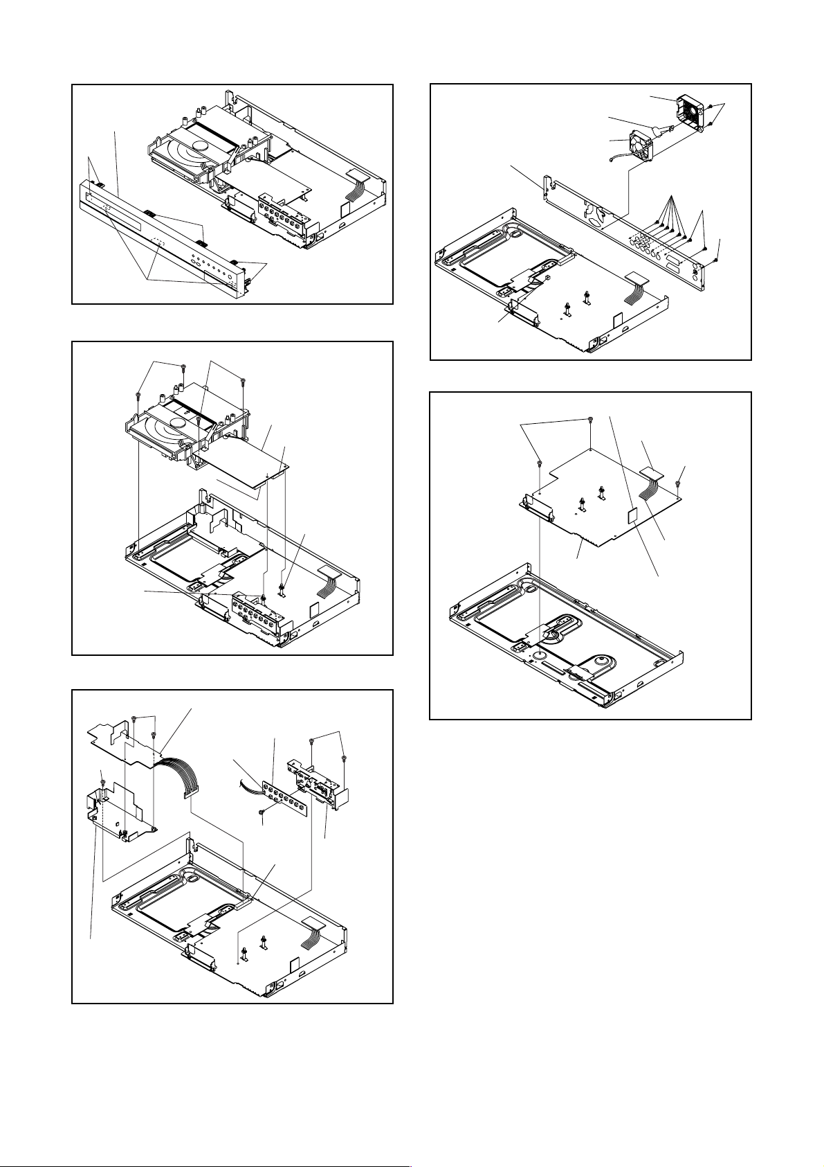
[2] PANEL
FRONT
(L-1)
(L-2)
LOCKING
CARD
SPACER
(S-2)
(S-2)
CN701
(L-1)
(L-1)
Fig. D2
[3] DVD MECHANISM
& DVD MAIN BOARD
ASSEMBLY
CN101
LOCKING
CARD
SPACER
FAN EARTH
[10] PANEL REAR
CN1601
(S-11)
[8] FAN COVER
[9] FAN
[13] BOARD AFV
[12] BOARD JACK
[11] BOARD
POWER
(S-7)
(S-9)
(S-10)
(S-8)
Fig. D5
(S-11)
Desolder
Desolder
(S-6)
[7] POWER
HOLDER
[6] BOARD POWER SUPPLY
(S-5)
[4] BOARD SWITCH
Desolder
(S-3)
CN1152
Fig. D3
Fig. D6
(S-4)
[5] BOARD
HOLDER
Fig. D4
1-5-2 E7B71DC
Page 14
3. How to Eject Manually
Note: When rotating the gear, be careful not to damage the gear.
1. Remove the COVER TOP.
2. Rotate the gear in the direction of the arrow manually as shown below until the tray descends.
3. Pull the tray out manually and remove a disc.
View for A
A
Rotate this gear in
the direction of the arrow
1-5-3 E7B71DC
Page 15
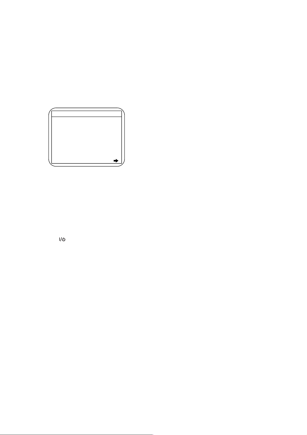
HOW TO INITIALIZE THE DVD RECORDER
To put the program back at the factory-default,
initialize the DVD recorder as the following procedure.
1. Turn the DVD recorder on.
2. Confirm that no disc is loaded or that the disc tray
is open. To put the DVD recorder into the Version
display mode, press [INSTANT SKIP], [1], [2], and
[3] buttons on the remote control in the order.
Fig. a appears on the screen.
*1: "
*2: Firmware Version differs depending on the
models, and this indication is one example.
" differs depending on the models.
*******
F/W VERSION DISP
MODEL NAME :
FE VERSION :
BE VERSION :
TT VERSION :
LD ADJUSTMENT :
DISC ADJUSTMENT :
DEFAULT SETTING : ENTER
EXIT : RETURN
*******
R30_011_00t
R3T32684U2B
T30025FSP
OK
OK
Fig. a Version Display Mode Screen
3. Press [ENTER] button, then the DVD recorder
starts initializing. When the initializing is
completed, the DVD recorder exits the Version
display mode and turns off the power
automatically.
* To move into the Normal mode from the
Version display mode, press [RETURN] button
on the remote control instead of [ENTER]
button.
* When [ ] button is pressed before [ENTER]
button is pressed, the DVD recorder exits the
Version display mode, then the power turns
off.
1-6-1 E7B71INT
Page 16
FIRMWARE RENEWAL MODE
1. Turn the power on and remove the disc on the tray.
2. To put the DVD recorder into version up mode,
press [INSTANT SKIP], [6], [5], and [4] buttons on
the remote control unit in the order. Then the tray
will open automatically.
Fig. a appears on the screen and Fig. b appears
on the VFD.
* Firmware Version differs depending on the
models, and this indication is one example.
Firm Update Mode
Please insert a disc.
Fig. a Version Up Mode Screen
Fig. b VFD in Version Up Mode
ver. R3T32684U2B
Current
F/W version
is displayed.
4. Select the firmware version pressing arrow
buttons, then press [ENTER].
Fig. d appears on the screen and Fig. e appears
on the VFD. The DVD recorder starts updating.
About VFD indication of Fig. e:
1) When Fig. d is displayed on the screen, “F-UP”
is displayed on the VFD.
2) When “Firmware Updating... XX% Complete.”
is displayed on the screen, “32684” is displayed
on the VFD.
* Firmware Version differs depending on the
models, and this indication is one example.
(*1)
Firm Update Mode
File Loading...
Fig. d Programming Mode Screen
ver.
R3T32684U2B
3. Load the disc for version up.
Fig. c appears on the screen. The file on the top is
highlighted as the default.
When there is only one file to exist, Step 4 will
start automatically.
* Firmware Version differs depending on the
models, and this indication is one example.
Firm Update Mode ver. R3T32684U2B
Disc name
is displayed.
VOL_200603130934
1 R3T32684U2B
2 R3T32685U2B
3 R3T32686U2B
4 R3T32687U2B
Fig. c Update Disc Screen
1 / 1
Files included
in the disc are
displayed.
Fig. e VFD in Programming Mode (Example)
The appearance shown in (*1) of Fig. d is
described as follows.
No. Appearance State
1 File Loading... Sending files into the memory
Firmware
2
Updating...
Writing new version data
XX% Complete.
Firmware
--Update Failure
Failed in updating
5. After updating is finished, the tray opens
automatically.
At this time, no button is available.
6. Pull out the AC code once, then insert it again.
1-7-1 E7B71FW
Page 17
NOTE: BOARD MEANS PRINTED CIRCUIT BOARD.
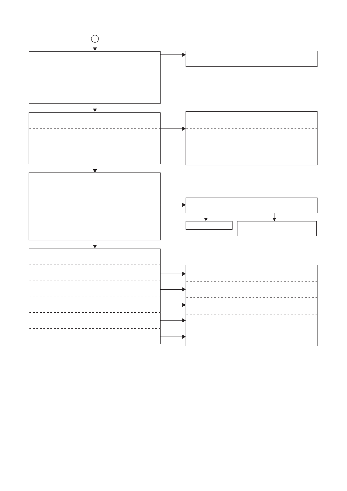
FLOW CHART NO.1
The power cannot be turned on.
TROUBLESHOOTING
Is the fuse normal?
Ye s
Is normal state restored when once unplugged
power cord is plugged again after several seconds.
Ye s
Is the al+5V line voltage normal?
Ye s
Check each rectifying circuit of secondary circuit
and service it if defective.
FLOW CHART NO.2
The fuse blows out.
Check the presence that the primary component
is leaking or shorted and service it if defective.
After servicing, replace the fuse.
FLOW CHART NO.3
When the output voltage fluctuates.
Does the secondary side photo coupler circuit
operate normally?
Ye s
Check the circuit and service it if defective.
(IC1001, D1008, D1009, D1010, D1014)
No
No
No
No
See FLOW CHART No.2 <The fuse blows out.>
Check for lead or short-circuiting of primary
circuit component and service it if defective.
(Q1001,Q1002,Q1003,T1001,D1001,D1002,
D1003,D1004,D1011,C1009,C1010)
Check the presence that the rectifying diode or circuit
is shorted in each rectifying circuit of secondary side
and service it if defective.
Check the circuit and service it if defective.
(IC1001, Q1101, D1111, D1113)
FLOW CHART NO.4
When buzz sound can be heard in the vicinity of power circuit.
Check if there is short circuit on the rectifying diode and the circuit in each rectifying circuit of secondary side and
service it if defective. (D1101,D1102,D1103,D1104,D1105,D1107,D1108,IC1151,IC1152,Q1154,Q1155,Q1156,
Q1158,Q1159,Q1160,Q1163)
FLOW CHART NO.5
-FL is not outputted.
Is the supply voltage of -30V fed to the anode of
No
D1104?
Ye s
Check for load circuit short-circuiting or leak, and
service it if defective.
Check D1104 and their periphery, and service it if
defective.
1-8-1 E7B71TR
Page 18
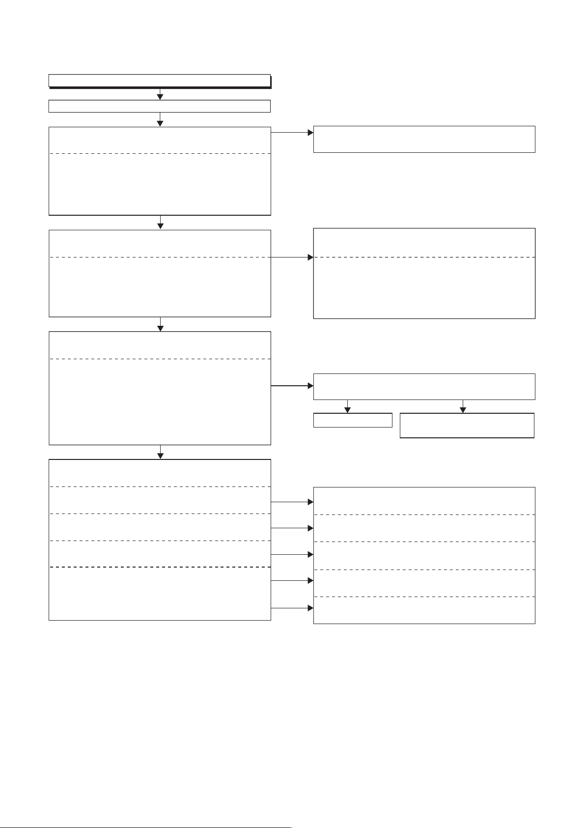
FLOW CHART NO.6
P-ON+10V is not outputted.
Is 12V voltage supplied to the collector of Q1160?
No
Is 12V voltage supplied to the emitter of Q1155?
Ye s
Is the "H" pulse outputted to Pin(53) of IC1501?
Ye s
Is the "L" pulse outputted to the collector of Q1157?
Ye s
Check Q1155 and their periphery, and service it
if defective.
FLOW CHART NO.7
AL+9V is not outputted.
Is 11V voltage supplied to the collector of Q1156?
Ye s
Check Q1156, D1156 and their periphery, and
service it if defective.
FLOW CHART NO.8
P-ON+5V(1) is not outputted.
Yes Check Q1160, D1162 and their periphery, and
service it if defective.
No
No
No
No
Check D1102, D1113, C1117, L1102 and their
periphery, and service it if defective.
Replace IC1501.
Replace Q1157.
Check D1102, D1113, D1170, D1171, C1117,
L1102 and their periphery, and service it if defective.
Is 5V voltage supplied to the
Check Q1154 and their periphery, and service it if
defective.
FLOW CHART NO.9
P-ON+5V(2) is not outputted.
Is 5V voltage supplied to the
Check Q1158 and their periphery, and service it if
defective.
FLOW CHART NO.10
EV+32V is not outputted.
Is the supply voltage 44V fed the cathode of D1103?
Check D1701 and their periphery and service it
if defective.
collector
Ye s
collector
Ye s
Ye s
of Q1154?
of Q1158?
No
No
No
Check D1108, L1101, C1114 , C1116 and their
periphery, and service it if defective.
Check D1108, L1105, C1120 and their
periphery, and service it if defective.
Check D1103, C1113 and their periphery, and
service it if defective.
FLOW CHART NO.11
AUDIO +5V is not outputted. (P-ON+10V is outputted normally.)
Is 6V voltage supplied to the base of Q1163?
Ye s
Replace Q1163.
No
1-8-2 E7B71TR
Check D1163, C1168 and their periphery, and
service it if defective.
Page 19
FLOW CHART NO.12
EV+3.3V is not outputted.
Is 5V voltage supplied to the collector of Q1159?
Ye s
Is the voltage of approximately 4V supplied to
the base of Q1159?
Ye s
Replace Q1159.
FLOW CHART NO.13
P-ON+2.5V is not outputted.
Is 4V voltage supplied to Pin(1) of IC1151?
Ye s
Replace IC1151.
FLOW CHART NO.14
P-ON+3.3V is not outputted.
Is 5V voltage supplied to Pin(1) of IC1152?
Ye s
Replace IC1152.
No
No
No
No
Check D1108, L1105, C1120 and their periphery,
and service it if defective.
Check IC1153 and their periphery, and service it if
defective.
Check D1105, C1110 and their periphery, and
service it if defective.
Check D1108, L1101, C1114, C1116 and their
periphery, and service it if defective.
FLOW CHART NO.15
The fluorescent display tube does not light up.
Is 3.3V voltage supplied to Pin(6, 24) of IC1503?
Ye s
Is approximately -24V to -28V voltage supplied to
Pin(15) of IC1503?
Ye s
Is there approximately 500kHz oscillation to
Pin(26) of IC1503?
Ye s
Are the filament voltage applied between (1)
and (24) of the fluorescent display tube?
Also negative voltage applied between these pins
and GND?
Ye s
Replace the fluorescent display tube.
No
No
No
No
Check the EV+3.3V line and service it if defective.
Check the -FL line and service it if defective.
Check R1560, IC1503 and their periphery, and
service it if defective.
Check the power circuit, D1101, D1112, C1106
and their periphery, and service it if defective.
1-8-3 E7B71TR
Page 20
FLOW CHART NO.16
The key operation is not functioning.
Are the contact point and the installation state of
the key switches normal?
Ye s
Is the control voltage normally inputted into
Pin(1, 2) of IC1501?
Ye s
Replace IC1501 or DVD MECHANISM & DVD
MAIN BOARD ASSEMBLY.
FLOW CHART NO.17
No operation is possible from the remote control unit. (
Is 5V voltage supplied to the Pin(3) terminal of
the RM1501 (remote control receiver)?
Ye s
Is the "L" pulse sent out from Pin(1) terminal of
the RM1501 (remote control receiver) when the
remote control unit is activated?
Ye s
Is the "L" pulse signal supplied to the Pin(27) of
IC1501?
Ye s
Replace IC1501 or DVD MECHANISM & DVD
MAIN BOARD ASSEMBLY.
No
Re-install some key switches correctly or
replace some key switches.
No
Check the key switches and their periphery, and
service it if defective.
3.300
2.479
2.464
1.746
1.730
1.115
1.100
0.484
0.469
0.161
0.146
(V)
Operation is possible from the unit.)
No
No
Check AL+5V (1) line and service it if defective.
Replace the RM1501 (remote control receiver).
Or replace remote control unit.
No
Check the line between the RM1501 (remote
control receiver) and the Pin(27) of IC1501, and
service it if defective.
KEYTerminal voltage of IC1501-1,2 -1
IC1501-1
REC
CH UP
REC
SPEED
CH
DOWN
OPEN
/CLOSE
KEY-2
IC1501-2
----------
REW
FWD
STOP
PLAY
POWER
FLOW CHART NO.18
The disc tray cannot be opened and closed. (It can be done using the remote control unit.)
Is the normal control voltage inputted to Pin(1) of
IC1501?
Refer to "FLOW CHART NO.16" <The key
No
Replace the "OPEN/CLOSE" button (SW3006).
operation is not functioning.>
Ye s
Refer to "FLOW CHART NO.19" <The disc tray
cannot be opened and closed.>
1-8-4 E7B71TR
Page 21
FLOW CHART NO.19
The disc tray cannot be opened and closed.
[No Disc] indicated.
Both functions of picture and sound do not operate normally.
Replace the DVD MECHANISM & DVD MAIN
BOARD ASSEMBLY.
FLOW CHART NO.20
VIDEO E-E does not appear normally.
Are the video signals inputted to each pin of
IC1201?
IC1201 VIDEO-IN 1 (AV1)16PIN
IC1201 VIDEO-IN (FRONT)14PIN
IC1201 Y-IN 1 (FRONT)7PIN
IC1201 C-IN 1 (FRONT)9PIN
IC1201 VIDEO-IN 2 (AV2/REAR)12PIN
IC1201 Y-IN 2 (REAR)100PIN
IC1201 C-IN 2 (REAR)1PIN
IC1201 TUNER-VIDEO
Are the video signals outputted to each pin of
IC1201?
IC1201 VIDEO-Y/CVBS-IN61PIN
IC1201 VIDEO-C-IN59PIN
Are the video signals outputted to each pin of
CN1201?
CN1201 VIDEO-Y/CVBS-IN10PIN
CN1201 VIDEO-C-IN8PIN
20PIN
Ye s
Ye s
No
No
No
Check the line between video input terminal and
each pin of IC1201.
IC1201 → JK120616PIN
IC1201 → JK12127PIN
IC1201 → JK12129PIN
IC1201 → JK200112PIN
IC1201 → JK1211100PIN
IC1201 → JK12111PIN
IC1201 → TU170120PIN
17PIN
Is 5V voltage supplied to the Pin(27,29,47,63) of IC1201?
Ye s
Replace IC1201. Check AL+5V(2) line
and service it if defective.
Check the line between each pin of IC1201 and
each pin of CN1201 and service it if defective.
IC1201
IC1201
→ CN120161PIN
→ CN1201 59PIN
VIDEO-IN 1 (AV1)
VIDEO-IN (FRONT)IC1201 → JK120114PIN
Y-IN 1 (FRONT)
C-IN 1 (FRONT)
VIDEO-IN 2 (AV2)
Y-IN 2 (REAR)
C-IN 2 (REAR)
TUNER-VIDEO
No
10PIN
VIDEO-Y/CVBS-IN
8PIN
VIDEO-C-IN
Continued to A on the next page.
1-8-5 E7B71TR
Page 22
A
Are the video signals outputted to each pin of
CN1201 on the BOARD POWER?
CN1201 VIDEO-Y(I/P)-OUT24PIN
CN1201 VIDEO-Y(I)-OUT30PIN
CN1201 VIDEO-Cr/Pr-OUT26PIN
CN1201 VIDEO-Cb/Pb-OUT28PIN
CN1201 VIDEO-C-OUT
Are the video signals shown above inputted into
each pin of IC1201?
IC1201 VIDEO-Y(I/P)-OUT51PIN
IC1201 VIDEO-Y(I)-OUT55PIN
IC1201 VIDEO-Cr/Pr-OUT52PIN
IC1201 VIDEO-Cb/Pb-OUT53PIN
IC1201 VIDEO-C-OUT57PIN
Are the video signals outputted to each pin of
IC1201?
IC1201 VIDEO-Y40PIN
IC1201 VIDEO-Cr/Pr39PIN
IC1201 VIDEO-Cb/Pb38PIN
IC1201 Y-OUT36PIN
IC1201 C-OUT34PIN
IC1201 VIDEO-OUT 1 (AV1)30PIN
IC1201 VIDEO-OUT 2 (AV2)22PIN
Are the video signals outputted to the specific
output terminal?
Are the luminance signals outputted to the
S-VIDEO OUT terminal (JK1213)?
Are the chroma signals outputted to the
S-VIDEO OUT terminal (JK1213)?
Are the Y, Cb, Cr signals outputted to the
COMPONENT OUT terminal (JK1205)?
Are the composite video signals outputted to
the VIDEO OUT (AV1) terminal (JK1206)?
Are the composite video signals outputted to
the VIDEO OUT (AV2) terminal (JK2001)?
22PIN
Ye s
Ye s
Ye s
No
No
No
No
No
No
No
No
Replace the DVD MECHANISM & DVD MAIN
BOARD ASSEMBLY.
Check the line between each pin of CN1201 and
each pin of IC1201, and service it if defective.
CN1201 → IC120124PIN
CN1201 → IC120126PIN
CN1201 → IC120128PIN
→ IC1201
22PIN
Is 5V voltage applied to the Pin(27,29,47,63) of
IC1201?
Ye s N o
Replace IC1201.
Check the periphery of JK1213 from
Pin (36) of IC1201 and service it if defective.
Check the periphery of JK1213 from
Pin (34) of IC1201 and service it if defective.
Check the periphery of JK1205 from Pin (38,39,
40) of IC1201 and service it if defective.
Check the periphery of JK1206 from Pin (30) of
IC1201 and service it if defective.
Check the periphery of JK2001 from Pin (22) of
IC1201 and service it if defective.
51PIN
52PIN
53PIN
57PINCN1201
Check AL+5V(2) line
and service it if defective.
VIDEO-Y(I/P)-OUT
VIDEO-Y(I)-OUTCN1201 → IC120130PIN 55PIN
VIDEO-Cr/Pr-OUT
VIDEO-Cb/Pb-OUT
VIDEO-C-OUT
1-8-6 E7B71TR
Page 23
FLOW CHART NO.21
Picture does not appear normally.
Set the disc on the disc tray, and playback.
Are the video signals outputted to each pin of
CN1201 on the BOARD POWER?
CN1201 VIDEO-Y(I/P)-OUT24PIN
CN1201 VIDEO-Y(I)-OUT30PIN
CN1201 VIDEO-Cr/Pr-OUT26PIN
CN1201 VIDEO-Cb/Pb-OUT28PIN
CN1201 VIDEO-C-OUT
Are the video signals shown above inputted into
each pin of IC1201?
IC1201 VIDEO-Y(I/P)-OUT51PIN
IC1201 VIDEO-Y(I)-OUT55PIN
IC1201 VIDEO-Cr/Pr-OUT52PIN
IC1201 VIDEO-Cb/Pb-OUT53PIN
IC1201 VIDEO-C-OUT57PIN
Are the video signals outputted to each pin of
IC1201?
IC1201 VIDEO-Y40PIN
IC1201 VIDEO-Cr/Pr39PIN
IC1201 VIDEO-Cb/Pb38PIN
IC1201 Y-OUT36PIN
IC1201 C-OUT34PIN
IC1201 VIDEO-OUT 1 (AV1)30PIN
IC1201 VIDEO-OUT 2 (AV2)22PIN
Are the video signals outputted to the specific
output terminal?
Are the luminance signals outputted to the
S-VIDEO OUT terminal (JK1213)?
Are the chroma signals outputted to the
S-VIDEO OUT terminal (JK1213)?
Are the Y, Cb, Cr signals outputted to the
COMPONENT OUT terminal (JK1205)?
Are the composite video signals outputted to
the VIDEO OUT (AV1) terminal (JK1206)?
Are the composite video signals outputted to
the VIDEO OUT (AV2) terminal (JK2001)?
22PIN
Ye s
Ye s
Ye s
No
No
No
No
No
No
No
No
Replace the DVD MECHANISM & DVD MAIN
BOARD ASSEMBLY.
Check the line between each pin of CN1201 and
each pin of IC1201, and service it if defective.
CN1201 → IC120124PIN
CN1201 → IC120126PIN
CN1201 → IC120128PIN
→ IC1201
22PIN
Is 5V voltage applied to the Pin(27,29,47,63) of
IC1201?
Ye s N o
Replace IC1201.
Check the periphery of JK1213 from
Pin (36) of IC1201 and service it if defective.
Check the periphery of JK1213 from
Pin (34) of IC1201 and service it if defective.
Check the periphery of JK1205 from Pin (38,39,
40) of IC1201 and service it if defective.
Check the periphery of JK1206 from Pin (30) of
IC1201 and service it if defective.
Check the periphery of JK2001 from Pin (22) of
IC1201 and service it if defective.
51PIN
52PIN
53PIN
57PINCN1201
Check AL+5V(2) line
and service it if defective.
VIDEO-Y(I/P)-OUT
VIDEO-Y(I)-OUTCN1201 → IC120130PIN 55PIN
VIDEO-Cr/Pr-OUT
VIDEO-Cb/Pb-OUT
VIDEO-C-OUT
1-8-7 E7B71TR
Page 24
FLOW CHART NO.22
Audio E-E does not appear normally.
Are the audio signals inputted to each pin of
IC1201?
IC1201 AUDIO-IN1 (AV1)93,94PIN
IC1201 AUDIO-IN1 (FRONT)91,92PIN
IC1201 AUDIO-IN2 (AV2)89,90PIN
IC1201 AUDIO-IN2 (REAR)81,82PIN
IC1201 TUNER-AUDIO84,85PIN
Ye s
Are the audio signals outputted to Pin(79,80) of
IC1201?
Ye s
Are the audio signals outputted to Pin(1,7) of
IC1203?
No (Rear
or Front
input)
No (Tuner)
No
No
Check the line between audio input terminal and
each pin of IC1201, and service it if defective.
IC1201
IC1201
IC1201
IC1201
Is SIF signal inputted to Pin(2) of IC2?
Are the audio signal outputted
to Pin(30,31) of IC1?
Check the line between
Pin(30,31) of IC1 and
Pin(84,85) of IC1201, and
service it if defective.
Is 5V voltage supplied to Pin(63) of IC1201?
Is 9V voltage supplied to Pin(75) of IC1201?
Replace IC1201.
Replace IC1203.
91,92PIN
81,82PIN
Ye s N o
→
JK120693,94PIN
→
JK1202,
JK1203
→
JK200189,90PIN
→
JK1204
Ye s
Ye s
Check the AL+5V(2) , AL+9V
line and service it if defective.
AUDIO-IN1 (AV1)
AUDIO-IN1 (FRONT)
AUDIO-IN2 (AV2)
AUDIO-IN2 (REAR)
Replace TU1701.
No
Replace IC1.
No
Continued to B on the next page.
1-8-8 E7B71TR
Page 25

B
Are the analog audio signals outputted to each pin
of CN1201 on BOARD POWER?
CN1201 14PIN AUDIO (L)-OUT
CN1201 16PIN AUDIO (R)-OUT
Ye s
Are the analog audio signals inputted to each pin
of IC1202?
IC1202 2PIN AUDIO (L)-OUT
IC1202 6PIN AUDIO (R)-OUT
Ye s
Do Pin(12) of CN1201 and Pin(37) of IC1501
become "H" level?
Ye s
Are the analog audio signals outputted to each pin
of IC1202?
IC1202 1PIN AUDIO (L)-OUT
IC1202 7PIN AUDIO (R)-OUT
Ye s
Are the analog audio signals inputted to each pin
of IC1201?
IC1201 77PIN AUDIO (L)-OUT
IC1201 76PIN AUDIO (R)-OUT
Ye s
Are the analog audio signals outputted to each pin
of IC1201?
IC1201 73,74PIN AUDIO-OUT 1 (AV1)
IC1201 71,72PIN AUDIO-OUT 2 (AV2)
IC1201 67,68PIN AUDIO-OUT 2 (REAR)
Ye s
Are the audio signals outputted to the specific
output terminal?
Are the audio signals outputted to the audio
terminal (JK1206)?
Are the audio signals outputted to the audio
terminal (JK2001)?
Are the audio signals outputted to the audio
terminal (JK1210)?
No
No
No
No
No
No
No
No
No
Replace the DVD MECHANISM & DVD MAIN
BOARD ASSEMBLY.
Check each line between each pin of CN1201
and each pin of IC1202, and service it if defective.
CN1201 14PIN → IC1202 2PIN AUDIO(L)-OUT
CN1201 16PIN → IC1202 6PIN AUDIO(R)-OUT
If Pin(12) of CN1201 become "L" level, replace
DVD MECHANISM & DVD MAIN BOARD
ASSEMBLY.
If Pin(37) of IC1501 become "L" level, replace
IC1501.
Replace IC1202.
Check each line between each pin of IC1202
and each pin of IC1201, and service it if defective.
IC1202 1PIN → IC1201 77PIN AUDIO(L)-OUT
IC1202 7PIN → IC1201 76PIN AUDIO(R)-OUT
Is 5V voltage supplied to Pin(63) of IC1201?
Is 9V voltage supplied to Pin(75) of IC1201?
Ye s N o
Replace IC1201.
Check the periphery between Pin(73,74) of IC1201
and the audio terminal (JK1206), and service it if
defective.
Check the periphery between Pin(71,72) of IC1201
and the audio terminal (JK2001), and service it if
defective.
Check the periphery between Pin(67,68) of IC1201
and the audio terminal (JK1210), and service it if
defective.
Check the AL+5V(2) , AL+9V
line and service it if defective.
1-8-9 E7B71TR
Page 26

FLOW CHART NO.23
Audio is not outputted during playback.
Set the disc on the disc tray, and playback.
Are the analog audio signals outputted to each pin
of CN1201 on BOARD POWER?
CN1201 14PIN AUDIO (L)-OUT
CN1201 16PIN AUDIO (R)-OUT
Ye s
Are the analog audio signals inputted to each pin
of IC1202?
IC1202 2PIN AUDIO (L)-OUT
IC1202 6PIN AUDIO (R)-OUT
Ye s
Do Pin(12) of CN1201 and Pin(37) of IC1501
become "H" level?
Ye s
Are the analog audio signals outputted to each pin
of IC1202?
IC1202 1PIN AUDIO (L)-OUT
IC1202 7PIN AUDIO (R)-OUT
Ye s
Are the analog audio signals inputted to each pin
of IC1201?
IC1201 77PIN AUDIO (L)-OUT
IC1201 76PIN AUDIO (R)-OUT
Ye s
Are the analog audio signals outputted to each pin
of IC1201?
IC1201 73,74PIN AUDIO-OUT 1 (AV1)
IC1201 71,72PIN AUDIO-OUT 2 (AV2)
IC1201 67,68PIN AUDIO-OUT 2 (REAR)
Ye s
Are the audio signals outputted to the specific
output terminal?
Are the audio signals outputted to the audio
terminal (JK1206)?
Are the audio signals outputted to the audio
terminal (JK2001)?
Are the audio signals outputted to the audio
terminal (JK1210)?
No
No
No
No
No
No
No
No
No
Replace the DVD MECHANISM & DVD MAIN
BOARD ASSEMBLY.
Check each line between each pin of CN1201
and each pin of IC1202, and service it if defective.
CN1201 14PIN → IC1202 2PIN AUDIO(L)-OUT
CN1201 16PIN → IC1202 6PIN AUDIO(R)-OUT
If Pin(12) of CN1201 become "L" level, replace
DVD MECHANISM & DVD MAIN BOARD
ASSEMBLY.
If Pin(37) of IC1501 become "L" level, replace
IC1501.
Replace IC1202.
Check each line between each pin of IC1202
and each pin of IC1201, and service it if defective.
IC1202 1PIN → IC1201 77PIN AUDIO(L)-OUT
IC1202 7PIN → IC1201 76PIN AUDIO(R)-OUT
Is 5V voltage supplied to Pin(63) of IC1201?
Is 9V voltage supplied to Pin(75) of IC1201?
Ye s N o
Replace IC1201.
Check the periphery between Pin(73,74) of IC1201
and the audio terminal (JK1206), and service it if
defective.
Check the periphery between Pin(71,72) of IC1201
and the audio terminal (JK2001), and service it if
defective.
Check the periphery between Pin(67,68) of IC1201
and the audio terminal (JK1210), and service it if
defective.
Check the AL+5V(2) , AL+9V
line and service it if defective.
1-8-10 E7B71TR
Page 27

FUNCTION INDICATOR SYMBOLS
Note: If an error occurs, a message with the error number appears on the screen.
Recording Error
Message Solution
Can not record on this disc.
This program is not allowed to
be recorded.
This program is not recordable
in Video mode.
This program is not allowed to
be recorded on this disc.
You cannot record on this disc as
Power Calibration Area is full.
Insert the recordable disc, and
ensure the disc status satisfies
the recording requirements.
You cannot record copy
prohibited programs.
Set “DVD-RW Recording
Format” to “VR mode”.
Insert a ver.1.1 CPRM
compatible DVD-RW disc.
Error message
E35
Error
No.
1 An error occurs during data reading. -
2
3
4 An error occurs with OPC. -
5 During recovery in a record. -
6
7 An error occurs in a format. -
8 It cannot start an encode. -
9
10
11
12
13 It is a reply that “ATAPI is not readable.” -
14
15
16 An error occurs in Finalize Close. -
17 An error occurs in Rec Stop Close. -
18 An error occurs in PCA Full (DVD_R). -
19 Safety Stop occurs during editing. -
20 High Speed Disc. 2
21 The disc is not formatted. 5
22 Disc Error has occurred. 3
23 The -R Disc of VR Mode. 6
24
25 During the Macrovision picture input. 11
26 During the CGMS picture input. 12
27
28
Error No.
Error Description Priority
There is no reply for 15 seconds in Test
Unit Ready.
Cannot write the data after trying three
times.
An error occurs even if recovery has been
tried three times.
NV_PCK/RDI_PCK is not in encoded
data.
Encode Pause condition continued for 10
minutes.
Encode Pause condition continued in
normal REC condition for 10 minutes.
Difference in the address and can not get
StreamID of RDI/VIDEO.
Cannot write the data after recovering
SMALL VMGI.
Cannot write the data after DVD-R
Reverse Track.
The disc except DVD-R/RW or finalized
DVD-R.
During the CGMS picture (possible to
record once) input. (Video Format Disc)
During the CGMS picture (possible to
record once) input. (Disc which is not for
the correspondence to VR Format
CPRM)
-
-
-
-
-
-
-
-
-
1
12
12
1-9-1 E7A70FIS
Page 28

Message Solution
This disc is protected and not
recordable.
Disc is full.
(No area for new recording)
You cannot record more than
99 titles on one disc.
(The maximum is 99.)
You cannot record more than
999 chapters on one disc.
(The maximum is 999.)
You cannot record on this disc
as Control Information is full.
You cannot record on the disc
as Power Calibration Area is
full.
This disc is already finalized.
Can not record on this disc. Repeat the same operation.
Release the disc protect
setting in the Disc Setting
menu.
Insert the recordable disc with
enough recording space.
Delete unnecessary titles.
Delete unnecessary chapter
markers.
Delete unnecessary titles. 34
Insert a new disc. 35 PCA is Full. (in REC start) 4
Release the finalizing for this
disc.
Error
No.
Error Description Priority
29 Disc Protected Disc. 7
30 No avilable recording space. 5
Its recording capacity has been reached.
31
(Video Format Disc)
Its recording capacity has been reached.
32
(VR Format Disc)
The 999 chapter has been reached. (VR
33
Format Disc)
There is not space to record field of
control information.
36 It is finalized. (Video Format Disc) 6
37 Access to Memory Area range outside. -
38 Sector Address is wrong. -
39 BUP writing error of chapter editing. -
7
8
9
10
If an error occurs during the timer recording, one of the following error numbers (40 to 42) or the above error
messages (error number: 1 to 39) is displayed on the recording menu after timer recording.
(Once the screen of the program line is exited, the program line for the error will be cleared.)
(No Error Message is displayed for the error No. 40 ~ 42.)
Timer Programming
The speed mode changes
to the error number.
Error Description Priority
A program with the error number is grayed out and asterisked on the timer programming list.
Message Solution
Error message is not
displayed.
2. ---
3. ---
4. ---
5. ---
6. ---
7. ---
8. ---
Error
No.
- Set the timer programming
correctly.
- Set the timer programming
before the start time.
Turn the power on and set the
clock correctly then set timer
programming again.
Insert the recordable disc. 42 No disc when recording -
- Some portion has not been recorded
because of program overlapping.
40
- Recording did not start at the start time.
41 Power failed -
-
1-9-2 E7A70FIS
Page 29

EXPLODED VIEWS
NOTE: BOARD MEANS PRINTED CIRCUIT BOARD.
Cabinet
2L031
See Electrical Parts List
for parts with this mark.
Some Ref. Numbers are
not in sequence.
2L021
( P2 )
DVD MECHANISM & DVD
MAIN BOARD ASSEMBLY
2L031
2L031
2L021
2L021
BOARD POWER SUPPLY
2B9
FM1001
A2
2L021
BOARD SWITCH
( P1 )
POWER ASSEMBLY
2L011
2B11
BOARD
JUNCTION
2B15
2L081
BOARD POWER
2L019
2L011
2L081
A6
2L021
2L012
2L013
2L021
2L081
2B1
BOARD JACK
2B12
2L081
A1X
A5
2B2
2B5
2L081
( P3 )
BOARD PSV
A4
2B3
2B4
( P4 )
BOARD AFV
2B13
NOTES
1. BOARD POWER and
BOARD SWITCH are
A5
supplied as an Assembly.
2. BOARD POWER SUPPLY,
BOARD JACK and BOARD
JUNCTION are supplied as
an Assembly.
( Refer to the Electrical Parts List )
1-17-1 E7B71CEX
Page 30

Packing
Some Ref. Numbers
are not in sequence.
X10X8X7 X4 X1
Unit
1-17-2 E7B71PEX
Page 31

MECHANICAL PARTS LIST
PRODUCT SAFETY NOTE: Products marked with a
! have special characteristics important to safety.
Before replacing any of these components, read
carefully the product safety notice in this service
manual. Don't degrade the safety of the product
through improper servicing.
Loca-
!
tion No.
A1X P000459750 1VM222036 PANEL FRONT E7B71BD
A2 P000459740 1VM120917 COVER TOP(R3 PAL) E7B70ED
A4 1VM120045A CHASSIS E6700ED
A5 0VM403657A FOOT K7010UA
A6 1VM220260 FAN COVER E6800ED
2B1 1VM220926A BOARD HOLDER E7A00UD
2B2 1VM422494 COVER CABLE E7A00UD
2B4 XP0U039WD001 LOCKING CARD SPACER KGLS-
2B5 1VM420990 POWER PLATE EARTH E6800ED
2B9 1VM322117 POWER HOLDER E7B20ED
2B13 1VM320610 PLATE GROUND(RCA) E6800ED
2B15 1VM320812 FAN EARTH E6800ED
FM1001 P000459880 MMEZL12NH008 MOTOR DC FAN D05U-12TS1
2L011 GBJP3060 SCREW P-TIGHT M3X6 BIND
2L012 GBHB3080 SCREW B-TIGHT M3X8 BIND
2L013 GBHP3080 SCREW P-TIGHT M3X8 BIND
2L021 GBCS3060 SCREW S-TIGHT M3X6 BIND
2L031 GBJS3100 SCREW S-TIGHT M3X10 BIND
2L081 GBJS3060 SCREW S-TIGHT M3X6 BIND
X1 P000459890 NB311BD REMOTE CONTROL UNIT
X4 P000460030 WPZ0122LG001 RF CORD PAL 1.2M
X7 P000459770 1VMN22905 QUICK GUIDE E7B71BD
X8 1VMN22863 REGISTE RATION CARD
X10 P000459760 1VMN22575 OWNERS MANUAL E7B71BD
TSB P/N Reference No. Description
22S
09(UX)
HEAD+
HEAD+
HEAD+ BLK
CROM
HEAD+
HEAD+
ACCESSORIES
NB311BD
E7B71BD
20060313 1-18-1 E7B71CA
Page 32

ELECTRICAL PARTS LIST
PRODUCT SAFETY NOTE: Products marked with a
! have special characteristics important to safety.
Before replacing any of these components, read
carefully the product safety notice in this service
manual. Don't degrade the safety of the product
through improper servicing.
NOTES:
1. Parts that are not assigned part numbers (---------)
are not available.
2. Tolerance of Capacitors and Resistors are noted
with the following symbols.
C.....±0.25% D.....±0.5% F.....±1%
G.....±2% J......±5% K.....±10%
M.....±20% N.....±30% Z.....+80/-20%
DVD MECHANISM & DVD MAIN
BOARD ASSEMBLY
Location
!
! P2 P000460160 N78E3CBN DVD MECHANISM & DVD MAIN
TSB P/N Reference No. Description
No.
BOARD ASSEMBLY
POWER ASSEMBLY
Location
!
! P1 P000459800 1VSA14365 POWER ASSEMBLY
BOARD POWER
Location
!
C1151 CE1CMASDL100 ELECTROLYTIC CAP. 10µF/
C1152 CE1CMASDL470 ELECTROLYTIC CAP. 47µF/
C1153 CE1CMASDL101 ELECTROLYTIC CAP. 100µF/
C1154 CE1CMASDL221 ELECTROLYTIC CAP. 220µF/
C1155 CCA1JZTFZ104 CERAMIC CAP.(AX) F Z 0.1µF/
C1160 CE1CMASDL470 ELECTROLYTIC CAP. 47µF/
C1163 CHD1JK30B103 CHIP CERAMIC CAP.(1608) B K
C1164 CE1CMASDL101 ELECTROLYTIC CAP. 100µF/
C1167 CE0KMASDL101 ELECTROLYTIC CAP. 100µF/
C1168 CE1CMASDL470 ELECTROLYTIC CAP. 47µF/
C1173 CE0KMASDL101 ELECTROLYTIC CAP. 100µF/
C1174 CE0KMASDL101 ELECTROLYTIC CAP. 100µF/
C1175 CE0KMASDL471 ELECTROLYTIC CAP. 470µF/
TSB P/N Reference No. Description
No.
Consists of the following:
---------- BOARD POWER (SUB-A)
---------- BOARD SWITCH (SUB-B)
TSB P/N Reference No. Description
No.
---------- BOARD POWER (SUB-A)
CAPACITORS
Consists of the following:
16V M
16V M
16V M
16V M
50V
16V M
0.01µF/50V
16V M
6.3V M
16V M
6.3V M
6.3V M
6.3V M
Location
!
C1176 CHD1JZ30F104 CHIP CERAMIC CAP.(1608) F Z
C1177 CHD1JZ30F104 CHIP CERAMIC CAP.(1608) F Z
C1202 CHD1JK30B102 CHIP CERAMIC CAP.(1608) B K
C1203 CHD1JZ30F104 CHIP CERAMIC CAP.(1608) F Z
C1206 CHD1JZ30F104 CHIP CERAMIC CAP.(1608) F Z
C1207 CHD1JZ30F104 CHIP CERAMIC CAP.(1608) F Z
C1208 CE1CMASDL221 ELECTROLYTIC CAP. 220µF/
C1209 CHD1JZ30F104 CHIP CERAMIC CAP.(1608) F Z
C1210 CE1CMASDL100 ELECTROLYTIC CAP. 10µF/
C1211 CE1CMASDL100 ELECTROLYTIC CAP. 10µF/
C1212 CHD1JJ3CH330 CHIP CERAMIC CAP.(1608) CH
C1213 CHD1JJ3CH330 CHIP CERAMIC CAP.(1608) CH
C1215 CHD1JZ30F104 CHIP CERAMIC CAP.(1608) F Z
C1216 CE0KMASDL101 ELECTROLYTIC CAP. 100µF/
C1218 CE0KMASDL471 ELECTROLYTIC CAP. 470µF/
C1221 CE1CMASDL100 ELECTROLYTIC CAP. 10µF/
C1222 CE1CMASDL100 ELECTROLYTIC CAP. 10µF/
C1223 CHD1JJ3CH271 CHIP CERAMIC CAP.(1608) CH
C1224 CHD1JJ3CH271 CHIP CERAMIC CAP.(1608) CH
C1225 CHD1JJ3CH470 CHIP CERAMIC CAP.(1608) CH
C1226 CHD1JJ3CH470 CHIP CERAMIC CAP.(1608) CH
C1227 CHD1JZ30F104 CHIP CERAMIC CAP.(1608) F Z
C1228 CE1CMASDL100 ELECTROLYTIC CAP. 10µF/
C1229 CE1CMASDL100 ELECTROLYTIC CAP. 10µF/
C1230 CE1JMASDLR47 ELECTROLYTIC CAP. 0.47µF/
C1231 CE1JMASDLR47 ELECTROLYTIC CAP. 0.47µF/
C1232 CE1JMASDLR47 ELECTROLYTIC CAP. 0.47µF/
C1233 CE1JMASDLR47 ELECTROLYTIC CAP. 0.47µF/
C1234 CE1JMASDLR47 ELECTROLYTIC CAP. 0.47µF/
C1235 CE1JMASDL1R0 ELECTROLYTIC CAP. 1µF/50V
C1236 CE1JMASDLR47 ELECTROLYTIC CAP. 0.47µF/
C1237 CHD1JZ30F104 CHIP CERAMIC CAP.(1608) F Z
C1238 CE1JMASDLR47 ELECTROLYTIC CAP. 0.47µF/
C1239 CE1EMASDL4R7 ELECTROLYTIC CAP. 4.7µF/
C1240 CE1JMASDLR47 ELECTROLYTIC CAP. 0.47µF/
C1241 CE1JMASDLR47 ELECTROLYTIC CAP. 0.47µF/
C1242 CE1JMASDLR47 ELECTROLYTIC CAP. 0.47µF/
C1243 CE1JMASDL1R0 ELECTROLYTIC CAP. 1µF/50V
C1244 CE1EMASDL4R7 ELECTROLYTIC CAP. 4.7µF/
TSB P/N Reference No. Description
No.
0.1µF/50V
0.1µF/50V
1000pF/50V
0.1µF/50V
0.1µF/50V
0.1µF/50V
16V M
0.1µF/50V
16V M
16V M
J 33pF/50V
J 33pF/50V
0.1µF/50V
6.3V M
6.3V M
16V M
16V M
J 270pF/50V
J 270pF/50V
J 47pF/50V
J 47pF/50V
0.1µF/50V
16V M
16V M
50V M
50V M
50V M
50V M
50V M
M
50V M
0.1µF/50V
50V M
25V M
50V M
50V M
50V M
M
25V M
20060313 1-19-1 E7B71EL
Page 33

Location
!
C1245 CHD1JZ30F104 CHIP CERAMIC CAP.(1608) F Z
C1246 CE1EMASDL4R7 ELECTROLYTIC CAP. 4.7µF/
C1247 CE1AMASDL470 ELECTROLYTIC CAP. 47µF/
C1248 CE1EMASDL4R7 ELECTROLYTIC CAP. 4.7µF/
C1249 CE1JMASDL1R0 ELECTROLYTIC CAP. 1µF/50V
C1250 CHD1JZ30F104 CHIP CERAMIC CAP.(1608) F Z
C1251 CE1EMASDL4R7 ELECTROLYTIC CAP. 4.7µF/
C1252 CE1EMASDL4R7 ELECTROLYTIC CAP. 4.7µF/
C1253 CE1JMASDL1R0 ELECTROLYTIC CAP. 1µF/50V
C1254 CE1EMASDL4R7 ELECTROLYTIC CAP. 4.7µF/
C1255 CE1EMASDL4R7 ELECTROLYTIC CAP. 4.7µF/
C1256 CHD1JZ30F104 CHIP CERAMIC CAP.(1608) F Z
C1257 CE1EMASDL4R7 ELECTROLYTIC CAP. 4.7µF/
C1258 CE1JMASDL1R0 ELECTROLYTIC CAP. 1µF/50V
C1259 CE1EMASDL4R7 ELECTROLYTIC CAP. 4.7µF/
C1260 CE1EMASDL4R7 ELECTROLYTIC CAP. 4.7µF/
C1261 CE1JMASDL1R0 ELECTROLYTIC CAP. 1µF/50V
C1262 CE0KMASDL470 ELECTROLYTIC CAP. 47µF/
C1263 CHD1JZ30F104 CHIP CERAMIC CAP.(1608) F Z
C1264 JW5.0T BOARD JUMPER D0.6-P5.0
C1265 CE1JMASDL1R0 ELECTROLYTIC CAP. 1µF/50V
C1266 CHD1JZ30F104 CHIP CERAMIC CAP.(1608) F Z
C1267 CE1CMASDL100 ELECTROLYTIC CAP. 10µF/
C1268 CHD1JZ30F104 CHIP CERAMIC CAP.(1608) F Z
C1269 CE1JMASDL1R0 ELECTROLYTIC CAP. 1µF/50V
C1270 CHD1JZ30F104 CHIP CERAMIC CAP.(1608) F Z
C1272 CHD1JZ30F104 CHIP CERAMIC CAP.(1608) F Z
C1273 CHD1JZ30F104 CHIP CERAMIC CAP.(1608) F Z
C1274 CE1JMASDL1R0 ELECTROLYTIC CAP. 1µF/50V
C1275 CHD1JZ30F104 CHIP CERAMIC CAP.(1608) F Z
C1276 CE0KMASDL470 ELECTROLYTIC CAP. 47µF/
C1277 CE1JMASDL1R0 ELECTROLYTIC CAP. 1µF/50V
C1278 CHD1JZ30F104 CHIP CERAMIC CAP.(1608) F Z
C1279 CE0KMASDL470 ELECTROLYTIC CAP. 47µF/
C1280 CE1JMASDL1R0 ELECTROLYTIC CAP. 1µF/50V
C1281 CE1JMASDL1R0 ELECTROLYTIC CAP. 1µF/50V
C1282 CE0KMASDL471 ELECTROLYTIC CAP. 470µF/
C1283 CE0KMASDL471 ELECTROLYTIC CAP. 470µF/
C1284 CCA1EKT0B104 CERAMIC CAP.(AX) B K 0.1µF/
C1285 CE1JMASDL1R0 ELECTROLYTIC CAP. 1µF/50V
C1286 CE0KMASDL471 ELECTROLYTIC CAP. 470µF/
TSB P/N Reference No. Description
No.
0.1µF/50V
25V M
10V M
25V M
M
0.1µF/50V
25V M
25V M
M
25V M
25V M
0.1µF/50V
25V M
M
25V M
25V M
M
6.3V M
0.1µF/50V
M
0.1µF/50V
16V M
0.1µF/50V
M
0.1µF/50V
0.1µF/50V
0.1µF/50V
M
0.1µF/50V
6.3V M
M
0.1µF/50V
6.3V M
M
M
6.3V M
6.3V M
25V
M
6.3V M
Location
!
No.
C1287 CE1JMASDL1R0 ELECTROLYTIC CAP. 1µF/50V
C1288 CE0KMASDL471 ELECTROLYTIC CAP. 470µF/
C1290 CE1JMASDL1R0 ELECTROLYTIC CAP. 1µF/50V
C1291 CE0KMASDL471 ELECTROLYTIC CAP. 470µF/
C1292 CE0KMASDL471 ELECTROLYTIC CAP. 470µF/
C1293 CE0KMASDL471 ELECTROLYTIC CAP. 470µF/
C1294 CE0KMASDL471 ELECTROLYTIC CAP. 470µF/
C1295 CHD1JZ30F104 CHIP CERAMIC CAP.(1608) F Z
C1296 CHD1JZ30F104 CHIP CERAMIC CAP.(1608) F Z
C1297 CE0KMASDL470 ELECTROLYTIC CAP. 47µF/
C1301 CHD1JK30B222 CHIP CERAMIC CAP. B K
C1302 CHD1JK30B222 CHIP CERAMIC CAP. B K
C1303 CE1CMASDL101 ELECTROLYTIC CAP. 100µF/
C1501 CHD1JJ3CH220 CHIP CERAMIC CAP.(1608) CH
C1502 CHD1JJ3CH180 CHIP CERAMIC CAP. CH J
C1504 CHD1JZ30F104 CHIP CERAMIC CAP.(1608) F Z
If C1507A is 0.015µF, then IC1502A is R3112N191A-TR-FA.
C1507A CHD1JK30B153 CHIP CERAMIC CAP.(1608) B K
IC1502A P000459990 QSZBA0TRC021 VOLTAGE DETECT
If C1507B is 0.1µF, then IC1502B is PST3619NR.
C1507B CHD1JK30B104 CHIP CERAMIC CAP.(1608) B K
IC1502B P000459980 QSZBA0TMM151 SYSTEM RESET IC
C1508 CCA1JZTFZ104 CERAMIC CAP.(AX) F Z 0.1µF/
C1509 CE0KMASDL471 ELECTROLYTIC CAP. 470µF/
C1510 CCA1JZTFZ104 CERAMIC CAP.(AX) F Z 0.1µF/
C1512 CHD1JJ3CH101 CHIP CERAMIC CAP.(1608) CH
C1515 CE1JMASDL220 ELECTROLYTIC CAP. 22µF/
C1517 CHD1JZ30F104 CHIP CERAMIC CAP.(1608) F Z
C1519 CHD1JZ30F104 CHIP CERAMIC CAP.(1608) F Z
C1520 CHD1JZ30F104 CHIP CERAMIC CAP.(1608) F Z
C1521 CE1JMASDL3R3 ELECTROLYTIC CAP. 3.3µF/
C1522 CHD1JJ3CH101 CHIP CERAMIC CAP.(1608) CH
C1523 CHD1JZ30F104 CHIP CERAMIC CAP.(1608) F Z
C1524 CE0KMASDL101 ELECTROLYTIC CAP. 100µF/
C1526 CE1CMASDL100 ELECTROLYTIC CAP. 10µF/
C1527 CE0KMASDL470 ELECTROLYTIC CAP. 47µF/
C1641 CHD1JJ3CH220 CHIP CERAMIC CAP.(1608) CH
C1645 CHD1JJ3CH270 CHIP CERAMIC CAP. CH J
C1646 CE1EMASDL4R7 ELECTROLYTIC CAP. 4.7µF/
C1647 CDA1EKS0X183 SEMICONDUCTOR CAP. SR K
C1648 CE1JMASDL1R0 ELECTROLYTIC CAP. 1µF/50V
TSB P/N Reference No. Description
M
6.3V M
M
6.3V M
6.3V M
6.3V M
6.3V M
0.1µF/50V
0.1µF/50V
6.3V M
2200pF/50V
2200pF/50V
16V M
J 22pF/50V
18pF/50V
0.1µF/50V
0.015µF/50V
R3112N191A-TR-FA
0.1µF/50V
PST3619NR
50V
6.3V M
50V
J 100pF/50V
50V M
0.1µF/50V
0.1µF/50V
0.1µF/50V
50V M
J 100pF/50V
0.1µF/50V
6.3V M
16V M
6.3V M
J 22pF/50V
27pF/50V
25V M
0.018µF/25V
M
20060313 1-19-2 E7B71EL
Page 34

Location
!
C1649 CE1JMASDL1R0 ELECTROLYTIC CAP. 1µF/50V
C1650 CHD1JK30B103 CHIP CERAMIC CAP.(1608) B K
C1651 CE0KMASDL470 ELECTROLYTIC CAP. 47µF/
C1704 CHD1JK30B103 CHIP CERAMIC CAP.(1608) B K
C1708 CHD1JZ30F104 CHIP CERAMIC CAP.(1608) F Z
C1709 CHD1JK30B103 CHIP CERAMIC CAP.(1608) B K
C1710 CHD1JK30B102 CHIP CERAMIC CAP.(1608) B K
C1711 CHD1JZ30F103 CHIP CERAMIC CAP. F Z
C1713 CHD1JZ30F103 CHIP CERAMIC CAP. F Z
C1714 CE1JMASDL100 ELECTROLYTIC CAP. 10µF/
C1715 CE1JMASDLR33 ELECTROLYTIC CAP. 0.33µF/
C1716 CE1CMASDL100 ELECTROLYTIC CAP. 10µF/
C1801 CHD1JK30B222 CHIP CERAMIC CAP. B K
C1803 CHD1JK30B222 CHIP CERAMIC CAP. B K
C1806 CHD1JK30B222 CHIP CERAMIC CAP. B K
C1807 CHD1JK30B102 CHIP CERAMIC CAP.(1608) B K
C1808 CHD1JK30B222 CHIP CERAMIC CAP. B K
C1809 CHD1JK30B222 CHIP CERAMIC CAP. B K
C1811 CE1JMASDL1R0 ELECTROLYTIC CAP. 1µF/50V
C1812 CHD1JK30B222 CHIP CERAMIC CAP. B K
C1813 CHD1JZ30F104 CHIP CERAMIC CAP.(1608) F Z
C1814 CHD1JK30B102 CHIP CERAMIC CAP.(1608) B K
C1816 CHD1JZ30F104 CHIP CERAMIC CAP.(1608) F Z
C1817 CE1JMASDL1R0 ELECTROLYTIC CAP. 1µF/50V
C1819 CHD1JK30B222 CHIP CERAMIC CAP. B K
C1820 CHD1JK30B222 CHIP CERAMIC CAP. B K
C1821 CHD1JK30B222 CHIP CERAMIC CAP. B K
C1823 CHD1JK30B222 CHIP CERAMIC CAP. B K
C1825 CE0KMASDL470 ELECTROLYTIC CAP. 47µF/
C1827 CHD1JK30B102 CHIP CERAMIC CAP.(1608) B K
C1831 CE1JMASDL1R0 ELECTROLYTIC CAP. 1µF/50V
C1834 CE0KMASDL470 ELECTROLYTIC CAP. 47µF/
TSB P/N Reference No. Description
No.
M
0.01µF/50V
6.3V M
0.01µF/50V
0.1µF/50V
0.01µF/50V
1000pF/50V
0.01µF/50V
0.01µF/50V
50V M
50V M
16V M
2200pF/50V
2200pF/50V
2200pF/50V
1000pF/50V
2200pF/50V
2200pF/50V
M
2200pF/50V
0.1µF/50V
1000pF/50V
0.1µF/50V
M
2200pF/50V
2200pF/50V
2200pF/50V
2200pF/50V
6.3V M
1000pF/50V
M
6.3V M
CONNECTORS
CN1152 J322C15TG001 242 SERIES CONNECTOR
CN1601 J3PHC02JG017 PH CONNECTOR (WHITE)
CN1701 E6851AFV AFV BOARD ASSEMBLY
224202115W1
TOP 2P B2B-PH-K-S(LF)
E6851BD
DIODES
D1151 NDLZ001N5397 DIODE 1N5397-B
D1154 NDLZ001N5397 DIODE 1N5397-B
D1156 NDTB00DZ10BS ZENER DIODE DZ-10BSBT265
D1157 JW5.0T BOARD JUMPER D0.6-P5.0
D1158 NDTZ01N4148M SWITCHING DIODE 1N4148M
D1159 NDTZ01N4148M SWITCHING DIODE 1N4148M
D1160 NDTZ01N4148M SWITCHING DIODE 1N4148M
Location
!
D1162 NDTB00DZ11BS ZENER DIODE DZ-11BSBT265
D1163 NDTB0DZ5R6BS ZENER DIODE DZ-
D1165 NDTZ01N4148M SWITCHING DIODE 1N4148M
D1166 NDTZ01N4148M SWITCHING DIODE 1N4148M
D1167 NDTZ01N4148M SWITCHING DIODE 1N4148M
D1170 NDQZ001N4005 RECTIFIER DIODE 1N4005
D1171 NDQZ001N4005 RECTIFIER DIODE 1N4005
D1172 NDQZ001N4005 RECTIFIER DIODE 1N4005
D1173 NDQZ001N4005 RECTIFIER DIODE 1N4005
D1174 NDTZ01N4148M SWITCHING DIODE 1N4148M
D1175 NDTZ01N4148M SWITCHING DIODE 1N4148M
D1501 NDTZ01N4148M SWITCHING DIODE 1N4148M
D1502 NDTA0DZ7R5BS ZENER DIODE DZ-7.5BSAT265
D1507 NDTC0DZ4R3BS ZENER DIODE DZ-
D1508 NDTC0DZ5R6BS ZENER DIODE DZ-
D1509 NDTZ01N4148M SWITCHING DIODE 1N4148M
D1601 NDTZ01N4148M SWITCHING DIODE 1N4148M
D1701 NDTB00DZ33BS ZENER DIODE DZ-33BSBT265
D1801 NDTA00DZ11BS ZENER DIODE DZ-11BSAT265
D1802 NDTA00DZ11BS ZENER DIODE DZ-11BSAT265
D1803 NDTA00DZ11BS ZENER DIODE DZ-11BSAT265
D1804 NDTA00DZ11BS ZENER DIODE DZ-11BSAT265
D1805 NDTA00DZ11BS ZENER DIODE DZ-11BSAT265
D1806 NDTA00DZ11BS ZENER DIODE DZ-11BSAT265
D1807 NDTA00DZ11BS ZENER DIODE DZ-11BSAT265
D1808 NDTA00DZ11BS ZENER DIODE DZ-11BSAT265
D1809 NDTA00DZ11BS ZENER DIODE DZ-11BSAT265
D1810 NDTA00DZ11BS ZENER DIODE DZ-11BSAT265
D1811 NDTC0DZ4R3BS ZENER DIODE DZ-
TSB P/N Reference No. Description
No.
5.6BSBT265
4.3BSCT265
5.6BSCT265
4.3BSCT265
ICS
IC1151 P000457260 QSZBA0SSH054 VOLTAGE REGULATOR
IC1152 P000457260 QSZBA0SSH054 VOLTAGE REGULATOR
IC1153 P000459940 NSZBA0TJY036 IC SHUNT REGULATOR
IC1201 P000459970 QSZBA0RHT051 IC INTERFACE HA118326APF-
IC1202 P000459910 NSZBA0SJY035 IC OP AMP KIA4558P/P
IC1203 P000457180 NSZBA0STY173 IC OP AMP RC4580IP
IC1501 P000459960 QSZAA0RMS051 MICROCONTROLLER 8BIT
If IC1502A is R3112N191A-TR-FA, then C1507A is 0.015µF.
IC1502A P000459990 QSZBA0TRC021 VOLTAGE DETECT
C1507A CHD1JK30B153 CHIP CERAMIC CAP.(1608) B K
If IC1502B is PST3619NR, then C1507B is 0.1µF.
IC1502B P000459980 QSZBA0TMM151 SYSTEM RESET IC
C1507B CHD1JK30B104 CHIP CERAMIC CAP.(1608) B K
IC1503 P000459930 NSZBA0T0S005 VFD DRIVER IC SC16313G
IC1641 P000460000 QSZBA0TSY018 IC VPS/PDC SLICER
PQ070XF01SZH
PQ070XF01SZH
KIA431-AT/P
E
MN101C77A FM
R3112N191A-TR-FA
0.015µF/50V
PST3619NR
0.1µF/50V
LC74793JM-TLM-E
COILS
L1201 LLAXKATTU101 INDUCTOR(100µH K)
L1203 LLBD00PKV022 CHOKE COIL 47µH
L1205 LLAXKATTU101 INDUCTOR(100µH K)
L1206 LLAXKATTU101 INDUCTOR(100µH K)
L1207 JW5.0T BOARD JUMPER D0.6-P5.0
L1209 LLAXKATTU101 INDUCTOR(100µH K)
L1501 LLAXKATTU101 INDUCTOR(100µH K)
LAP02TA101K
LAP02TA101K
LAP02TA101K
LAP02TA101K
LAP02TA101K
20060313 1-19-3 E7B71EL
Page 35

Location
!
L1502 LLAXKATTU101 INDUCTOR(100µH K)
L1703 LLAXKATTU100 INDUCTOR 10µH-K-26T
L1801 LLAXKATTU101 INDUCTOR(100µH K)
L1802 LLAXKATTUR47 INDUCTOR(0.47µH K)
L1803 1VSA11351 BEAD CORE ASSEMBLY
TSB P/N Reference No. Description
No.
LAP02TA101K
LAP02TA101K
LAP02TAR47K
E6820ED
TRANSISTORS
Q1154 NQS4KTC3266P TRANSISTOR KTC3266-GR-
Q1155 NQSYKTA1273P TRANSISTOR KTA1273-Y-AT/P
Q1156 QQSK2SC2001A TRANSISTOR 2SC2001-T-A-K
Q1157 NQSYKTC3199P TRANSISTOR KTC3199-Y-AT/P
Q1158 NQSYKTC3203P TRANSISTOR KTC3203-Y-AT/P
Q1159 NQSYKTC3199P TRANSISTOR KTC3199-Y-AT/P
Q1160 NQSYKTC3199P TRANSISTOR KTC3199-Y-AT/P
Q1163 NQSYKTC3199P TRANSISTOR KTC3199-Y-AT/P
Q1164 NQSZKRC103MP NPN TRANSISTOR KRC103M-
Q1201 NQSYKTC3199P TRANSISTOR KTC3199-Y-AT/P
Q1202 NQSYKTC3199P TRANSISTOR KTC3199-Y-AT/P
Q1203 NQSZKRC103MP NPN TRANSISTOR KRC103M-
Q1204 NQS4KTA1266P TRANSISTOR KTA-1266-GR-
Q1205 NQSZKRC103MP NPN TRANSISTOR KRC103M-
Q1207 NQSYKTC3199P TRANSISTOR KTC3199-Y-AT/P
Q1501 NQS5KTC3199P TRANSISTOR KTC3199-BL-AT/
Q1502 NQSZKRC103MP NPN TRANSISTOR KRC103M-
Q1503 NQSZKRC103MP NPN TRANSISTOR KRC103M-
Q1504 NQSYKTA1267P TRANSISTOR KTA1267-Y-AT/P
Q1505 NQSYKTC3199P TRANSISTOR KTC3199-Y-AT/P
Q1506 QF1GSSM3K15F MOS FET SSM3K15F(TE85L F)
Q1507 QF1GSSM3K15F MOS FET SSM3K15F(TE85L F)
Q1508 NQSYKTC3203P TRANSISTOR KTC3203-Y-AT/P
Q1602 NQSYKTC3199P TRANSISTOR KTC3199-Y-AT/P
Q1801 NQSYKTA1267P TRANSISTOR KTA1267-Y-AT/P
Q1802 NQS4KTA1266P TRANSISTOR KTA-1266-GR-
Q1803 NQSYKTC3199P TRANSISTOR KTC3199-Y-AT/P
Q1804 NQSYKTC3199P TRANSISTOR KTC3199-Y-AT/P
Q1805 NQSYKTC3199P TRANSISTOR KTC3199-Y-AT/P
Q1806 NQSYKTC3199P TRANSISTOR KTC3199-Y-AT/P
Q1807 NQSYKTC3199P TRANSISTOR KTC3199-Y-AT/P
Q1810 NQSYKTC3199P TRANSISTOR KTC3199-Y-AT/P
Q1811 NQSYKTC3199P TRANSISTOR KTC3199-Y-AT/P
Q1812 NQSYKTC3199P TRANSISTOR KTC3199-Y-AT/P
Q1813 NQSYKTC3199P TRANSISTOR KTC3199-Y-AT/P
Q1814 NQSYKTC3199P TRANSISTOR KTC3199-Y-AT/P
AT / P
AT / P
AT / P
AT / P
AT / P
P
AT / P
AT / P
AT / P
RESISTORS
R1151 RRXAZR5Z0000 CHIP RES.(1608) 1/10W 0 Ω
R1152 RCX4JATZ0102 CARBON RES. 1/4W J 1k Ω
R1155 RCX4JATZ0102 CARBON RES. 1/4W J 1k Ω
R1156 RCX4JATZ05R6 CARBON RES. 1/4W J 5.6 Ω
R1157 RCX4JATZ08R2 CARBON RES. 1/4W J 8.2 Ω
R1158 RCX4JATZ0391 CARBON RES. 1/4W J 390 Ω
R1159 RRXAJR5Z0473 CHIP RES. 1/10W J 47k Ω
R1160 JW5.0T BOARD JUMPER D0.6-P5.0
R1162 RCX4JATZ0561 CARBON RES. 1/4W J 560 Ω
R1163 RCX4JATZ0561 CARBON RES. 1/4W J 560 Ω
R1164 RCX4JATZ0561 CARBON RES. 1/4W J 560 Ω
R1165 RCX4JATZ0561 CARBON RES. 1/4W J 560 Ω
R1167 RCX4JATZ0152 CARBON RES. 1/4W J 1.5k Ω
R1170 RRXAJR5Z0472 CHIP RES. 1/10W J 4.7k Ω
R1171 RCX4JATZ0681 CARBON RES. 1/4W J 680 Ω
Location
!
R1172 RCX4JATZ0681 CARBON RES. 1/4W J 680 Ω
R1173 RRXAJR5Z0471 CHIP RES. 1/10W J 470 Ω
R1174 RCX4JATZ0391 CARBON RES. 1/4W J 390 Ω
R1175 RRXAJR5Z0151 CHIP RES. 1/10W J 150 Ω
R1176 RRXAJR5Z0331 CHIP RES. 1/10W J 330 Ω
R1177 RRXAJR5Z0151 CHIP RES. 1/10W J 150 Ω
R1178 RRXAFR5H4701 CHIP RES. 1/10W F 4.7k Ω
R1179 RRXAFR5H1501 CHIP RES. 1/10W F 1.5k Ω
R1180 RRXAFR5H1000 CHIP RES. 1/10W F 100 Ω
R1182 JW5.0T BOARD JUMPER D0.6-P5.0
R1183 RRXAJR5Z0471 CHIP RES. 1/10W J 470 Ω
R1184 RRXAJR5Z0471 CHIP RES. 1/10W J 470 Ω
R1186 RRXAFR5H1002 CHIP RES. 1/10W F 10k Ω
R1187 RRXAFR5H1002 CHIP RES. 1/10W F 10k Ω
R1188 RRXAFR5H1502 CHIP RES. 1/10W F 15k Ω
R1189 RRXAFR5H1002 CHIP RES. 1/10W F 10k Ω
R1190 RRXAFR5H2701 CHIP RES. 1/10W F 2.7k Ω
R1191 RRXAFR5H1200 CHIP RES. 1/10W F 120 Ω
R1192 RRXAFR5H1501 CHIP RES. 1/10W F 1.5k Ω
R1193 RRXAJR5Z0222 CHIP RES. 1/10W J 2.2k Ω
R1194 RRXAJR5Z0222 CHIP RES. 1/10W J 2.2k Ω
R1195 RRXAJR5Z0102 CHIP RES. 1/10W J 1k Ω
R1199 RRXAJR5Z0473 CHIP RES. 1/10W J 47k Ω
R1200 RRXAJR5Z0472 CHIP RES. 1/10W J 4.7k Ω
R1201 RRXAFR5H2400 CHIP RES. 1/10W F 240 Ω
R1202 RRXAFR5H2000 CHIP RES. 1/10W F 200 Ω
R1203 RRXAFR5H2000 CHIP RES. 1/10W F 200 Ω
R1204 RRXAFR5H2000 CHIP RES. 1/10W F 200 Ω
R1205 RRXAFR5H2200 CHIP RES. 1/10W F 220 Ω
R1207 RRXAJR5Z0102 CHIP RES. 1/10W J 1k Ω
R1208 RRXAJR5Z0332 CHIP RES. 1/10W J 3.3k Ω
R1209 RRXAJR5Z0302 CHIP RES. 1/10W J 3k Ω
R1210 RRXAJR5Z0302 CHIP RES. 1/10W J 3k Ω
R1214 RRXAJR5Z0471 CHIP RES. 1/10W J 470 Ω
R1215 RRXAJR5Z0471 CHIP RES. 1/10W J 470 Ω
R1216 RCX4JATZ0102 CARBON RES. 1/4W J 1k Ω
R1217 RCX4JATZ0331 CARBON RES. 1/4W J 330 Ω
R1219 RRXAJR5Z0123 CHIP RES. 1/10W J 12k Ω
R1220 RRXAJR5Z0123 CHIP RES. 1/10W J 12k Ω
R1221 RRXAFR5H3302 CHIP RES. 1/10W F 33.0k Ω
R1222 RRXAFR5H3302 CHIP RES. 1/10W F 33.0k Ω
R1224 RCX6JATZ0682 CARBON RES. 1/6W J 6.8k Ω
R1225 RRXAJR5Z0682 CHIP RES. 1/10W J 6.8k Ω
R1226 RRXAJR5Z0683 CHIP RES. 1/10W J 68k Ω
R1227 RRXAJR5Z0683 CHIP RES. 1/10W J 68k Ω
R1228 RRXAFR5H8201 CHIP RES. 1/10W F 8.2k Ω
R1229 RRXAFR5H8201 CHIP RES. 1/10W F 8.2k Ω
R1230 RRXAFR5H1302 CHIP RES. 1/10W F 13k Ω
R1231 RRXAJR5Z0133 CHIP RES. 1/10W J 13k Ω
R1232 RRXAFR5H1302 CHIP RES. 1/10W F 13k Ω
R1233 RRXAJR5Z0133 CHIP RES. 1/10W J 13k Ω
R1234 RRXAJR5Z0104 CHIP RES. 1/10W J 100k Ω
R1235 RRXAJR5Z0104 CHIP RES. 1/10W J 100k Ω
R1236 RRXAJR5Z0471 CHIP RES. 1/10W J 470 Ω
R1237 RRXAJR5Z0471 CHIP RES. 1/10W J 470 Ω
R1238 RRXAJR5Z0103 CHIP RES. 1/10W J 10k Ω
R1239 RCX4JATZ0750 CARBON RES. 1/4W J 75 Ω
R1244 RRXAJR5Z0105 CHIP RES. 1/10W J 1M Ω
R1245 RRXAJR5Z0105 CHIP RES. 1/10W J 1M Ω
R1246 RRXAJR5Z0105 CHIP RES. 1/10W J 1M Ω
R1247 RRXAJR5Z0105 CHIP RES. 1/10W J 1M Ω
R1248 RRXAJR5Z0183 CHIP RES. 1/10W J 18k Ω
R1249 RRXAJR5Z0183 CHIP RES. 1/10W J 18k Ω
R1250 RCX6JATZ0151 CARBON RES. 1/6W J 150 Ω
R1251 RRXAFR5H3301 CHIP RES. 1/10W F 3.3k Ω
R1253 RCX4JATZ0681 CARBON RES. 1/4W J 680 Ω
TSB P/N Reference No. Description
No.
20060313 1-19-4 E7B71EL
Page 36

Location
!
R1254 RRXAJR5Z0221 CHIP RES. 1/10W J 220 Ω
R1501 RCX4JATZ0821 CARBON RES. 1/4W J 820 Ω
R1502 RRXAJR5Z0101 CHIP RES. 1/10W J 100 Ω
R1504 RRXAJR5Z0103 CHIP RES. 1/10W J 10k Ω
R1505 RRXAJR5Z0103 CHIP RES. 1/10W J 10k Ω
R1506 RRXAJR5Z0103 CHIP RES. 1/10W J 10k Ω
R1508 RRXAJR5Z0103 CHIP RES. 1/10W J 10k Ω
R1510 RRXAJR5Z0473 CHIP RES. 1/10W J 47k Ω
R1511 RRXAJR5Z0393 CHIP RES. 1/10W J 39k Ω
R1513 RRXAZR5Z0000 CHIP RES.(1608) 1/10W 0 Ω
R1515 RRXAJR5Z0332 CHIP RES. 1/10W J 3.3k Ω
R1516 RRXAJR5Z0471 CHIP RES. 1/10W J 470 Ω
R1517 RRXAJR5Z0332 CHIP RES. 1/10W J 3.3k Ω
R1518 RRXAJR5Z0823 CHIP RES. 1/10W J 82k Ω
R1519 RRXAJR5Z0473 CHIP RES. 1/10W J 47k Ω
R1520 RRXAJR5Z0101 CHIP RES. 1/10W J 100 Ω
R1521 RRXAJR5Z0101 CHIP RES. 1/10W J 100 Ω
R1522 RRXAJR5Z0101 CHIP RES. 1/10W J 100 Ω
R1525 RRXAJR5Z0101 CHIP RES. 1/10W J 100 Ω
R1527 RRXAJR5Z0103 CHIP RES. 1/10W J 10k Ω
R1528 RRXAJR5Z0223 CHIP RES. 1/10W J 22k Ω
R1531 RRXAJR5Z0101 CHIP RES. 1/10W J 100 Ω
R1532 RRXAJR5Z0103 CHIP RES. 1/10W J 10k Ω
R1533 RRXAJR5Z0223 CHIP RES. 1/10W J 22k Ω
R1534 RCX6JATZ0101 CARBON RES. 1/6W J 100 Ω
R1535 RRXAJR5Z0473 CHIP RES. 1/10W J 47k Ω
R1536 RRXAJR5Z0101 CHIP RES. 1/10W J 100 Ω
R1537 RRXAJR5Z0101 CHIP RES. 1/10W J 100 Ω
R1540 RRXAJR5Z0101 CHIP RES. 1/10W J 100 Ω
R1542 RRXAJR5Z0473 CHIP RES. 1/10W J 47k Ω
R1543 RRXAZR5Z0000 CHIP RES.(1608) 1/10W 0 Ω
R1544 RRXAZR5Z0000 CHIP RES.(1608) 1/10W 0 Ω
R1545 RRXAJR5Z0473 CHIP RES. 1/10W J 47k Ω
R1546 RRXAJR5Z0473 CHIP RES. 1/10W J 47k Ω
R1548 RRXAJR5Z0472 CHIP RES. 1/10W J 4.7k Ω
R1549 RRXAJR5Z0473 CHIP RES. 1/10W J 47k Ω
R1551 RRXAJR5Z0472 CHIP RES. 1/10W J 4.7k Ω
R1553 RRXAJR5Z0471 CHIP RES. 1/10W J 470 Ω
R1554 RRXAJR5Z0103 CHIP RES. 1/10W J 10k Ω
R1555 RRXAJR5Z0103 CHIP RES. 1/10W J 10k Ω
R1556 RRXAJR5Z0102 CHIP RES. 1/10W J 1k Ω
R1557 RRXAJR5Z0102 CHIP RES. 1/10W J 1k Ω
R1559 RRXAJR5Z0102 CHIP RES. 1/10W J 1k Ω
R1560 RRXAJR5Z0683 CHIP RES. 1/10W J 68k Ω
R1561 RRXAZR5Z0000 CHIP RES.(1608) 1/10W 0 Ω
R1563 RRXAJR5Z0682 CHIP RES. 1/10W J 6.8k Ω
R1564 JW5.0T BOARD JUMPER D0.6-P5.0
R1565 JW5.0T BOARD JUMPER D0.6-P5.0
R1566 RCX4JATZ0561 CARBON RES. 1/4W J 560 Ω
R1567 RRXAJR5Z0473 CHIP RES. 1/10W J 47k Ω
R1568 RRXAJR5Z0473 CHIP RES. 1/10W J 47k Ω
R1569 RRXAJR5Z0473 CHIP RES. 1/10W J 47k
R1570 RRXAJR5Z0473 CHIP RES. 1/10W J 47k Ω
R1571 RRXAJR5Z0473 CHIP RES. 1/10W J 47k Ω
R1572 JW5.0T BOARD JUMPER D0.6-P5.0
R1604 RCX4JATZ0820 CARBON RES. 1/4W J 82 Ω
R1605 RRXAJR5Z0102 CHIP RES. 1/10W J 1k Ω
R1606 RRXAJR5Z0102 CHIP RES. 1/10W J 1k Ω
R1645 RRXAJR5Z0272 CHIP RES. 1/10W J 2.7k Ω
R1646 RRXAZR5Z0000 CHIP RES.(1608) 1/10W 0 Ω
R1647 RRXAZR5Z0000 CHIP RES.(1608) 1/10W 0 Ω
R1648 RRXAJR5Z0103 CHIP RES. 1/10W J 10k Ω
R1649 RRXAJR5Z0103 CHIP RES. 1/10W J 10k Ω
R1650 RRXAJR5Z0562 CHIP RES. 1/10W J 5.6k Ω
R1651 RRXAJR5Z0103 CHIP RES. 1/10W J 10k Ω
R1652 RRXAJR5Z0101 CHIP RES. 1/10W J 100 Ω
TSB P/N Reference No. Description
No.
Location
!
R1706 RCX6JATZ0332 CARBON RES. 1/6W J 3.3k Ω
R1707 RCX6JATZ0222 CARBON RES. 1/6W J 2.2k Ω
R1708 RRXAZR5Z0000 CHIP RES.(1608) 1/10W 0 Ω
R1709 RRXAZR5Z0000 CHIP RES.(1608) 1/10W 0 Ω
R1710 RRXAJR5Z0331 CHIP RES. 1/10W J 330 Ω
R1711 RRXAJR5Z0331 CHIP RES. 1/10W J 330 Ω
R1712 RRXAJR5Z0331 CHIP RES. 1/10W J 330 Ω
R1713 RRXAJR5Z0331 CHIP RES. 1/10W J 330 Ω
R1714 RRXAZR5Z0000 CHIP RES.(1608) 1/10W 0 Ω
R1801 RRXAJR5Z0750 CHIP RES. 1/10W J 75 Ω
R1802 RRXAJR5Z0750 CHIP RES. 1/10W J 75 Ω
R1803 RRXAJR5Z0750 CHIP RES. 1/10W J 75 Ω
R1804 RRXAJR5Z0102 CHIP RES. 1/10W J 1k Ω
R1806 RRXAJR5Z0102 CHIP RES. 1/10W J 1k Ω
R1808 RRXAJR5Z0223 CHIP RES. 1/10W J 22k Ω
R1809 RRXAJR5Z0223 CHIP RES. 1/10W J 22k Ω
R1810 RRXAZR5Z0000 CHIP RES.(1608) 1/10W 0 Ω
R1812 RRXAJR5Z0103 CHIP RES. 1/10W J 10k Ω
R1813 RCX6JATZ0303 CARBON RES. 1/6W J 30k Ω
R1814 RRXAJR5Z0182 CHIP RES. 1/10W J 1.8k Ω
R1815 RRXAJR5Z0222 CHIP RES. 1/10W J 2.2k Ω
R1816 RCX4JATZ0750 CARBON RES. 1/4W J 75 Ω
R1817 RCX6JATZ0911 CARBON RES. 1/6W J 910 Ω
R1818 RRXAJR5Z0222 CHIP RES. 1/10W J 2.2k Ω
R1819 RRXAJR5Z0750 CHIP RES. 1/10W J 75 Ω
R1820 RCX4JATZ0471 CARBON RES. 1/4W J 470 Ω
R1821 RCX4JATZ0471 CARBON RES. 1/4W J 470 Ω
R1822 RRXAJR5Z0221 CHIP RES. 1/10W J 220 Ω
R1824 RRXAJR5Z0750 CHIP RES. 1/10W J 75 Ω
R1825 RRXAJR5Z0102 CHIP RES. 1/10W J 1k Ω
R1826 RRXAJR5Z0102 CHIP RES. 1/10W J 1k Ω
R1827 RCX6JATZ0911 CARBON RES. 1/6W J 910 Ω
R1829 RCX4JATZ0750 CARBON RES. 1/4W J 75 Ω
R1830 RCX4JATZ0750 CARBON RES. 1/4W J 75 Ω
R1831 RCX4JATZ0750 CARBON RES. 1/4W J 75 Ω
R1833 RCX4JATZ0750 CARBON RES. 1/4W J 75 Ω
R1834 RCX4JATZ0750 CARBON RES. 1/4W J 75 Ω
R1835 RRXAJR5Z0750 CHIP RES. 1/10W J 75 Ω
R1836 RRXAJR5Z0750 CHIP RES. 1/10W J 75 Ω
R1837 RRXAJR5Z0750 CHIP RES. 1/10W J 75 Ω
R1840 RRXAJR5Z0221 CHIP RES. 1/10W J 220 Ω
R1841 RRXAJR5Z0221 CHIP RES. 1/10W J 220 Ω
R1842 RRXAJR5Z0104 CHIP RES. 1/10W J 100k Ω
R1844 RRXAJR5Z0750 CHIP RES. 1/10W J 75 Ω
R1845 RCX6JATZ0101 CARBON RES. 1/6W J 100 Ω
R1848 RRXAJR5Z0102 CHIP RES. 1/10W J 1k Ω
R1849 RRXAJR5Z0102 CHIP RES. 1/10W J 1k Ω
R1850 RRXAJR5Z0221 CHIP RES. 1/10W J 220 Ω
R1851 RRXAJR5Z0221 CHIP RES. 1/10W J 220 Ω
R1853 RRXAJR5Z0750 CHIP RES. 1/10W J 75 Ω
R1854 RRXAJR5Z0472 CHIP RES. 1/10W J 4.7k
Ω
R1855 RRXAJR5Z0472 CHIP RES. 1/10W J 4.7k Ω
R1856 RRXAJR5Z0472 CHIP RES. 1/10W J 4.7k Ω
R1857 RRXAJR5Z0472 CHIP RES. 1/10W J 4.7k Ω
R1858 RRXAJR5Z0103 CHIP RES. 1/10W J 10k Ω
R1859 RRXAJR5Z0471 CHIP RES. 1/10W J 470 Ω
R1860 RRXAJR5Z0473 CHIP RES. 1/10W J 47k Ω
R1861 RRXAJR5Z0472 CHIP RES. 1/10W J 4.7k Ω
TSB P/N Reference No. Description
No.
Ω
MISCELLANEOUS
2B3 1VM320515 FL HOLDER E6700UD
FL1501 P000457330 TVFD1C0FT048 VACUUM FLUORESCENT
JK1201 P000457110 JXRL010LY135 JACK RCA(YELLOW) MTJ-032-
JK1202 P000457120 JXRL010LY136 JACK RCA(WHITE) MTJ-032-
JK1203 P000457090 JYRL010LY029 JACK RCA(RED) MTJ-032-05A-
DISPLAY 7-BT-301N
05B-20(B110)
05B-22(B110)
21(B110)
20060313 1-19-5 E7B71EL
Page 37

Location
!
JK1204 P000459860 JXRL020LY123 PIN JACK 2P MSD-242V-01 NI
JK1205 P000457140 JXRL030LY132 JACK RCA 3PIN MSD-243V-18
JK1206 P000459850 JXGL210LY008 RGB CONNECTOR MRC-
JK1209 P000457100 JXRL010LY125 JACK RCA(BLACK) MSP-251V-
JK1210 P000459860 JXRL020LY123 PIN JACK 2P MSD-242V-01 NI
JK1211 P000457070 JXEL040LY003 JACK S TYPE MDC-050V-2.4
JK1212 P000457080 JXEL040RP003 MINI DIN SOCKET MDC1-34-
JK1213 P000457070 JXEL040LY003 JACK S TYPE MDC-050V-2.4
JW001 P000460040 WX1E6820-002 FFC CABLE 30P FFC/P1.00/70
JW002 P000460040 WX1E6820-002 FFC CABLE 30P FFC/P1.00/70
JW010 P000460060 WX1E6820-006 FLAT CABLE 3P AWG26#2651/
JW011 P000460090 WX1E7B20-003 1PIN WIRE AWG26/UL1007
RM1501 P000457340 USESJRSKK039 REMOTE RECEIVER PIC-
TU1701 P000460020 UTUNPLGAL017 TUNER UNIT TMFE2-301A
X1501 P000459810 FXC323LQUA02 XTAL QTF38-32768K125P20L
X1502 P000459830 FY0805PMR002 CERAMIC RESONETOR
X1641 P000459820 FXC445LDS003 Xtal 1K*044335DA
TSB P/N Reference No. Description
No.
FE LF
NI FE LF
021V-05 ABS(B110
01 NI FE LF
FE LF
LF(B110
020
LF(B110
P2.0/100
TR-64/7
37043LU
CSTLS8M00G56-B0
BOARD SWITCH
Location
!
TSB P/N Reference No. Description
No.
----------
BOARD SWITCH (SUB-B)
Consists of the following:
RESISTORS
R3003 RRXAJR5Z0301 CHIP RES. 1/10W J 300 Ω
R3004 RRXAJR5Z0621 CHIP RES. 1/10W J 620 Ω
R3005 RRXAJR5Z0102 CHIP RES. 1/10W J 1k Ω
R3006 RRXAJR5Z0222 CHIP RES. 1/10W J 2.2k Ω
R3007 RRXAJR5Z0682 CHIP RES. 1/10W J 6.8k Ω
R3010 RRXAJR5Z0301 CHIP RES. 1/10W J 300 Ω
R3012 RRXAJR5Z0222 CHIP RES. 1/10W J 2.2k Ω
R3015 RRXAJR5Z0621 CHIP RES. 1/10W J 620 Ω
R3016 RRXAJR5Z0102 CHIP RES. 1/10W J 1k Ω
R3017 RRXAJR5Z0682 CHIP RES. 1/10W J 6.8k Ω
SWITCHES
SW3001 P000460010 SST0101HH003 TACT SWITCH KSM0612B
SW3002 P000460010 SST0101HH003 TACT SWITCH KSM0612B
SW3003 P000460010 SST0101HH003 TACT SWITCH KSM0612B
SW3004 P000460010 SST0101HH003 TACT SWITCH KSM0612B
SW3005 P000460010 SST0101HH003 TACT SWITCH KSM0612B
SW3006 P000460010 SST0101HH003 TACT SWITCH KSM0612B
SW3007 P000460010 SST0101HH003 TACT SWITCH KSM0612B
SW3008 P000460010 SST0101HH003 TACT SWITCH KSM0612B
SW3009 P000460010 SST0101HH003 TACT SWITCH KSM0612B
SW3011 P000460010 SST0101HH003 TACT SWITCH KSM0612B
BOARD PSV
Location
!
! P3 P000459790 1VSA14349 BOARD PSV
TSB P/N Reference No. Description
No.
---------- BOARD POWER SUPPLY (PSV-
---------- BOARD JUNCTION (PSV-B)
---------- BOARD JACK (PSV-C)
Consists of the following:
A)
BOARD POWER SUPPLY
Location
!
! C1001 CT2E683DC011 METALIZED FILM CAP. 0.068µF/
! C1002 CE1CMASDL100 ELECTROLYTIC CAP. 10µF/16V
C1003 CCD1JZSYV223 CERAMIC CAP. YV Z 0.022µF/
! C1004 CCN2EMA0E222 SAFTY CAP. 2200pF/250V
C1005 CA2H101S6016 ELECTROLYTIC CAP. 100µF/
C1006 CCA1CKT0X182 CERAMIC CAP.(AX) X K 1800pF/
C1008 CCA1JKT0B102 CERAMIC CAP.(AX) B K 1000pF/
C1009 CCD3AKPSL560 CERAMIC CAP. SL K 56pF/1KV
C1010 CCD2JKP0B103 CERAMIC CAP. B K 0.01µF/500V
C1101 CCD2JKP0B471 CERAMIC CAP. B K 470pF/500V
C1104 CHD1JK30B333 CHIP CERAMIC CAP.(1608) B K
C1106 CE1CMASDL101 ELECTROLYTIC CAP. 100µF/
C1107 CE1JMASDL220 ELECTROLYTIC CAP. 22µF/50V
C1108 CHD1JK30B103 CHIP CERAMIC CAP.(1608) B K
C1109 CHD1JZ30F104 CHIP CERAMIC CAP.(1608) F Z
C1110 CE0KMASDL102 ELECTROLYTIC CAP. 1000µF/
C1111 CE0KMZADL332 ELECTROLYTIC CAP. 3300µF/
C1112 CE1CMASDL102 ELECTROLYTIC CAP. 1000µF/
C1113 CE1JMASDL100 ELECTROLYTIC CAP. 10µF/50V
C1114 CE0KMZADL472 ELECTROLYTIC CAP. 4700µF/
C1115 CHD1JK30B103 CHIP CERAMIC CAP.(1608) B K
C1116 CE0KMASDL102 ELECTROLYTIC CAP. 1000µF/
C1117 CE1CMASDL471 ELECTROLYTIC CAP. 470µF/
C1120 CE0KMASDL102 ELECTROLYTIC CAP. 1000µF/
D1001 NDLZ001N5397 DIODE 1N5397-B
D1002 NDLZ001N5397 DIODE 1N5397-B
D1003 NDLZ001N5397 DIODE 1N5397-B
D1004 NDLZ001N5397 DIODE 1N5397-B
D1005 NDTZ01N4148M SWITCHING DIODE 1N4148M
D1006 NDTZ01N4148M SWITCHING DIODE 1N4148M
D1007 NDTZ01N4148M SWITCHING DIODE 1N4148M
D1008 NDTZ01N4148M SWITCHING DIODE 1N4148M
D1009 NDTZ01N4148M SWITCHING DIODE 1N4148M
D1010 NDTZ01N4148M SWITCHING DIODE 1N4148M
D1011 NDQZ000BA159 RECTIFIER DIODE BA159
D1013 JW5.0T BOARD JUMPER D0.6-P5.0
D1101 NDQZ000BA157 RECTIFIER DIODE BA157
D1102 NDQZ000SB380 SCHOTTKY BARRIER DIODE
D1103 NDQZ000BA157 RECTIFIER DIODE BA157
D1104 NDQZ000BA157 RECTIFIER DIODE BA157
D1105 NDQZ000SB140 SCHOTTKY BARRIER DIODE
D1107 NDQZ000SB240 SCHOTTKY BARRIER DIODE
D1108 NDQZ000SB340 SCHOTTKY BARRIER DIODE
D1111 NDTB0DZ6R8BS ZENER DIODE DZ-6.8BSBT265
D1112 NDTA00DZ20BS ZENER DIODE DZ-20BSAT265
D1113 NDTB00DZ15BS ZENER DIODE DZ-15BSBT265
TSB P/N Reference No. Description
No.
----------
CAPACITORS
DIODES
BOARD POWER SUPPLY (PSV-A)
Consists of the following:
250V K
M
50V
400V M
16V
50V
0.033µF/50V
16V M
M
0.01µF/50V
0.1µF/50V
6.3V M
6.3V SL
16V M
M
6.3V SL
0.01µF/50V
6.3V M
16V M
6.3V M
SB380
SB140
SB240-B/P
SB340
20060313 1-19-6 E7B71EL
Page 38

Location
!
TSB P/N Reference No. Description
No.
IC
! IC1001 P000459900 NPEA000EL817 PHOTOCOUPLER EL817A
COILS
L1001 1VSA11355 BEAD CORE ASSEMBLY
L1002 1VSA11355 BEAD CORE ASSEMBLY
L1003 1VSA11355 BEAD CORE ASSEMBLY
! L1004 LLBG00ZTU022 LINE FILTER 56MH
L1005 XL03010XM001 BEAD CORE B16 RH
L1101 LLC150KKV007 POWER INDUCTORS
L1102 LLC180KKV007 POWER INDUCTORS
L1105 LLBD00PKV022 CHOKE COIL 47µH
E6820ED
E6820ED
E6820ED
TLF14CB5630R2
3.5X10X1.3
TWKBNP-150K
TWKBNP-180K
TRANSISTORS
Q1001 NQSYKTC3199P TRANSISTOR KTC3199-Y-AT/P
Q1002 QQS12SC1815F TRANSISTOR 2SC1815-
! Q1003 QFWZ02SK3566 FET 2SK3566
Q1101 NQSYKTA1267P TRANSISTOR KTA1267-Y-AT/P
GR(TE2 F T)
RESISTORS
! R1001 RCX2565FS001 CARBON RES. 1/2W K 5.6M Ω
R1002 RCX4JATZ0564 CARBON RES. 1/4W J 560k Ω
R1003 RCX4JATZ0564 CARBON RES. 1/4W J 560k Ω
R1004 RCX6JATZ0104 CARBON RES. 1/6W J 100k Ω
R1005 RCX6JATZ0103 CARBON RES. 1/6W J 10k Ω
R1006 RCX6JATZ0474 CARBON RES. 1/6W J 470k Ω
R1007 RCX6JATZ0104 CARBON RES. 1/6W J 100k Ω
R1009 RCX4JATZ0105 CARBON RES. 1/4W J 1M Ω
R1010 RCX4JATZ0105 CARBON RES. 1/4W J 1M Ω
R1011 RCX4JATZ0105 CARBON RES. 1/4W J 1M Ω
R1012 RCX6JATZ0152 CARBON RES. 1/6W J 1.5k Ω
R1013 RCX4GATZ0821 CARBON RES. 1/4W G 820 Ω
R1014 RCX6JATZ0104 CARBON RES. 1/6W J 100k Ω
R1016 RN01JZLZ02R7 METAL OXIDE FILM RES. 1W J
R1017 RCX6JATZ0562 CARBON RES. 1/6W J 5.6k Ω
R1018 RCX4JATZ0102 CARBON RES. 1/4W J 1k Ω
R1019 RN02823ZU001 METAL OXIDE FILM RES. 2W J
R1020 RN011R8ZU001 METAL OXIDE FILM RES. 1W J
R1101 RRXAJR5Z0102 CHIP RES. 1/10W J 1k Ω
R1102 RRXAZR5Z0000 CHIP RES.(1608) 1/10W 0 Ω
R1103 RRXAJR5Z0472 CHIP RES. 1/10W J 4.7k Ω
R1104 RRXAJR5Z0182 CHIP RES. 1/10W J 1.8k Ω
R1105 RRXAZR5Z0000 CHIP RES.(1608) 1/10W 0 Ω
R1106 RRXAFR5H0222 CHIP RES.(1608) 1/10W F 2.2k
R1108 RRXAFR5H0562 CHIP RES. 1/10W F 5.6k Ω
R1109 RCX4JATZ0102 CARBON RES. 1/4W J 1k Ω
2.7 Ω
82k Ω
1.8 Ω
Ω
MISCELLANEOUS
2B11 1VM420987 HEAT SINK E6800ED
2L019 GBJS3080 SCREW S-TIGHT M3X8 BIND
! AC1001 WAB0182LW016 POWER CORD
! F1001 P000459950 PAGC20BW3162 FUSE T1.6AL/250V
FH1001 XH01Z00LY002 FUSE HOLDER MSF-015 LF
FH1002 XH01Z00LY002 FUSE HOLDER MSF-015 LF
SA1001 P000457210 NVQZ10D471KB SURGE ABSORBER 470V+-
! T1001 P000459870 LTTZPE0XB003 TRANS POWER BCK-28-9980
HEAD+
PE8G2X91H0AA061
(B110)
(B110)
10PER
BOARD JUNCTION
Location
!
TSB P/N Reference No. Description
No.
----------
BOARD JUNCTION (PSV-B)
Consists of the following:
CONNECTOR
CN1106 JCTUB15TG002 242 SERIES CONNECTOR
TUC-P15X-B1 WHT ST
MISCELLANEOUS
JW1001 P000460050 WX1E6820-005 FLAT CABLE 8P AWG26#2651/
JW1002 P000460070 WX1E6820-007 FLAT CABLE 7P AWG26#2651/
P2.0/70
P2.0/70
BOARD JACK
Location
!
C2002 CCA1CKT0X222 CERAMIC CAP.(AX) X K 2200pF/
C2004 CCA1CKT0X222 CERAMIC CAP.(AX) X K 2200pF/
C2005 CHD1JJ3CH471 CHIP CERAMIC CAP.(1608) CH
C2006 CHD1JK30B222 CHIP CERAMIC CAP. B K
C2007 CHD1JJ3CH471 CHIP CERAMIC CAP.(1608) CH
C2008 CCA1JKT0B102 CERAMIC CAP.(AX) B K 1000pF/
C2009 CE1JMASDL1R0 ELECTROLYTIC CAP. 1µF/50V
C2010 CE1JMASDL1R0 ELECTROLYTIC CAP. 1µF/50V
C2011 CHD1JK30B102 CHIP CERAMIC CAP.(1608) B K
C2021 CE0KMASDL471 ELECTROLYTIC CAP. 470µF/
C2022 CE1CMASDL101 ELECTROLYTIC CAP. 100µF/
D2001 NDTA00DZ11BS ZENER DIODE DZ-11BSAT265
D2002 NDTA00DZ11BS ZENER DIODE DZ-11BSAT265
D2003 NDTA00DZ11BS ZENER DIODE DZ-11BSAT265
D2004 NDTA00DZ11BS ZENER DIODE DZ-11BSAT265
D2005 NDTA00DZ11BS ZENER DIODE DZ-11BSAT265
D2006 NDTA00DZ11BS ZENER DIODE DZ-11BSAT265
D2007 NDTA00DZ11BS ZENER DIODE DZ-11BSAT265
D2008 NDTA00DZ11BS ZENER DIODE DZ-11BSAT265
D2009 NDTA00DZ11BS ZENER DIODE DZ-11BSAT265
D2010 NDTA00DZ11BS ZENER DIODE DZ-11BSAT265
L2003 1VSA11351 BEAD CORE ASSEMBLY
Q2001 NQSYKTC3199P TRANSISTOR KTC3199-Y-AT/P
Q2002 NQSYKTC3199P TRANSISTOR KTC3199-Y-AT/P
Q2003 NQS4KTA1266P TRANSISTOR KTA-1266-GR-AT/
R2001 RRXAJR5Z0221 CHIP RES. 1/10W J 220 Ω
R2002 RCX4JATZ0750 CARBON RES. 1/4W J 75 Ω
R2003 RRXAJR5Z0750 CHIP RES. 1/10W J 75 Ω
R2004 RCX4JATZ0681 CARBON RES. 1/4W J 680 Ω
R2005 RCX4JATZ0821 CARBON RES. 1/4W J 820 Ω
R2006 RCX6JATZ0472 CARBON RES. 1/6W J 4.7k Ω
R2007 RCX4JATZ0821 CARBON RES. 1/4W J 820 Ω
R2008 RCX6JATZ0472 CARBON RES. 1/6W J 4.7k Ω
R2009 RRXAJR5Z0750 CHIP RES. 1/10W J 75 Ω
R2010 RRXAJR5Z0750 CHIP RES. 1/10W J 75 Ω
R2011 RRXAJR5Z0750 CHIP RES. 1/10W J 75 Ω
TSB P/N Reference No. Description
No.
----------
CAPACITORS
DIODES
COIL
TRANSISTORS
RESISTORS
BOARD JACK (PSV-C)
Consists of the following:
16V
16V
J 470pF/50V
2200pF/50V
J 470pF/50V
50V
M
M
1000pF/50V
6.3V M
16V M
E6820ED
P
20060313 1-19-7 E7B71EL
Page 39

Location
!
R2012 RRXAJR5Z0102 CHIP RES. 1/10W J 1k Ω
R2013 RRXAJR5Z0102 CHIP RES. 1/10W J 1k Ω
R2014 RRXAJR5Z0750 CHIP RES. 1/10W J 75 Ω
TSB P/N Reference No. Description
No.
MISCELLANEOUS
2B12 1VM423185 21P PLATE EARTH E7B20ED
JK2001 P000459840 JXGL210LY006 RGB CONNECTOR MRC-021V-
JW2001 P000460080 WX1E7B20-002 FLAT CABLE 15P AWG26#2651/
03 ABS(B11
P2.0/70
BOARD AFV
Location
!
P4 P000459780 1VSA12358
C1 CHD1JZ30F104 CHIP CERAMIC CAP.(1608) F Z
C4 CHD1JJ3CH560 CHIP CERAMIC CAP. CH J
C5 CHD1JJ3CH220 CHIP CERAMIC CAP.(1608) CH
C6 CHD1JJ3CH560 CHIP CERAMIC CAP. CH J
C7 CHD1JC3CH3R0 CHIP CERAMIC CAP. CH C 3pF/
C8 CHD1JC3CH3R0 CHIP CERAMIC CAP. CH C 3pF/
C11 CHD1JK30B103 CHIP CERAMIC CAP.(1608) B K
C12 CE1CMASSL100 ELECTROLYTIC CAP. 10µF/16V
C13 CHD1JK30B103 CHIP CERAMIC CAP.(1608) B K
C14 CHD1JK30B103 CHIP CERAMIC CAP.(1608) B K
C15 CE1CMASSL100 ELECTROLYTIC CAP. 10µF/16V
C16 CE1CMASSL100 ELECTROLYTIC CAP. 10µF/16V
C17 CHD1JZ30F104 CHIP CERAMIC CAP.(1608) F Z
C19 CHD1JZ30F104 CHIP CERAMIC CAP.(1608) F Z
C20 CE1JMASSL3R3 ELECTROLYTIC CAP. 3.3µF/50V
C21 CHD1JZ30F104 CHIP CERAMIC CAP.(1608) F Z
C22 CE1CMASSL100 ELECTROLYTIC CAP. 10µF/16V
C24 CE1JMASSLR22 ELECTROLYTIC CAP. 0.22µF/
C27 CCA1JZTFZ104 CERAMIC CAP.(AX) F Z 0.1µF/
CN1 JTED009ER045 ANGLE PIN HEADER 9P IMSA-
D2 NDTZ01N4148M SWITCHING DIODE 1N4148M
IC1 P000459920 NSZBA0SP3005 IC AUDIO PROCESSOR
L1 LLAXKATTU100 INDUCTOR 10µH-K-26T
L2 JW5.0T BOARD JUMPER D0.6-P5.0
L3 LLAXKATTU180 INDUCTOR 18µH-K-26T
L4 LLAXKATTU100 INDUCTOR 10µH-K-26T
R1 RRXAJR5Z0102 CHIP RES. 1/10W J 1k Ω
R4 RRXAJR5Z0124 CHIP RES. 1/10W J 120k Ω
R5 RRXAZR5Z0000 CHIP RES.(1608) 1/10W 0 Ω
R6 RRXAZR5Z0000 CHIP RES.(1608) 1/10W 0 Ω
X1 FXD186LLN001 XTAL 18.432MHz
TSB P/N Reference No. Description
No.
CAPACITORS
CONNECTOR
DIODE
IC
COILS
RESISTORS
MISCELLANEOUS
BOARD AFV
Consists of the following:
0.1µF/50V
56pF/50V
J 22pF/50V
56pF/50V
50V
50V
0.01µF/50V
M H7
0.01µF/50V
0.01µF/50V
M H7
M H7
0.1µF/50V
0.1µF/50V
M H7
0.1µF/50V
M H7
50V M H7
50V
6029B-1-09Z003-
MSP3417G-QG-B8-V3
20060313 1-19-8 E7B71EL
Page 40

Page 41

SERVICE MANUAL
DVD Video Recorder
FILE NO. 810-200617GR
®
D-R160SB
The above model is classified as a green product (*1), as indicated by the underlined serial
number. This Service Manual describes replacement parts for the green product. When
repairing this green product, use the part(s) described in this manual and lead-free solder (*2).
For (*1) and (*2), see the next page.
TOSHIBA CORPORATION 2006
Published in Japan, Mar. 2006 GREEN
Page 42

System Control Block Diagram
NOTE: BOARD MEANS PRINTED CIRCUIT BOARD.
TO POWER SUPPLY
BLOCK DIAGRAM
REG-CONT
PWSW
BLOCK DIAGRAMS
IC1501
(SUB MICRO CONTROLLER)
52
REG-CONT
RESET
P-DOWN
14
30
53
PWSW
IC1502
RESET
1 2
Q1504
EV+3.3V
IC101
(MAIN MICRO CONTROLLER)
SYS-RESET
SYS-RESET
SUB-RXD
SUB-TXD
SUB-SCLK
CLK 27 IN
CLK 27 OUT
P-ON+1.2V
IC106
DVD MAIN BOARD
RDY
+1.2V
REGULATOR
N23
N24
L25
R24
T4
J25
N2
N1
CN701
44SYS-RESET
11SUB-RXD
33SUB-TXD
55SUB-SCLK
22RDY
X802
27MHz
X'TAL
VI+1.2V
CN101 CN1151
30 301V2CONT
CN1201
X1502
8MHz
RESONATOR
X1501
32.768KHz
X'TAL
8
OSC2
9
OSC1
12
X OUT
X IN
11
22
SYS-RESET
19
SUB-RXD
18
SUB-TXD
20
SUB-SCLK
RDY
29
26
1V2CONT
BUP+3.3V
FL-DIN
FL-CLK
FL-STB
REMOTE
FAN-CONT2
DAVN-L
DVD-AUDIO-MUTE
AUDIO-MUTE
SCART-AUDIO-MUTE
SUB-SDA
SUB-SCL
7
48
50
49
27
55
24
37
38
39
33
34
Q1602
Q1506
C1509
(BACKUP CAPACITOR)
RM1501
REMOTE
SENSOR
Q1507
28
1
2
IC1503
DIN
CLK
STB
Q1505
(VFD DRIVER)
FAN-AL+12V
1G
23
~
~
7G
17
a
7
~
~
h
14
i
16
CN1601
SCART-AUDIO-MUTE
EV+5V
GRID
SEGMENT
1 FAN+12V
2 FAN-GND
SDA
SCL
DAVN-L
DVD-AUDIO-MUTE
AUDIO-MUTE
SDA
SCL
TU1701(TUNER UNIT)
SCL
9
SDA
10
FL1501
VFD
TO VIDEO
BLOCK DIAGRAM
TO AUDIO
BLOCK DIAGRAM
FAN
KEY SWITCH
CN3001
KEY SWITCH
BOARD SWITCH
1
2
KEY-2
1
2
1
KEY-1
2
KEY-2
CN1502
KEY-1
BOARD POWER
1-10-1
E7B71BLS
Page 43

Digital Signal Process Block Diagram
NOTE: BOARD MEANS PRINTED CIRCUIT BOARD.
DVD MECHANISM
BOARD
ENCODER
FE
ENCODER
SLED
MOTOR
M
SPINDLE
MOTOR
M
PICK
-UP
TRAY OPEN
CN1003
CN1002
TILT
TRACKING
FOCUS
CN1001
BOARD
RELAY
CN201
CN301
+3.3V
IC201
RF/
ERROR AMP
IC301
MOTOR
DRIVER
IC202
IC302
LPC
OP AMP
MOTOR
DRIVER
DVD MAIN BOARD
IC101
FRONT-END
DIGITAL
SIGNAL
PROCESS
BACK-END
DIGITAL
SIGNAL
PROCESS
REC VIDEO SIGNAL PB VIDEO SIGNAL REC AUDIO SIGNAL PB AUDIO SIGNAL
G4
D/A
D/A
M4
VIDEO
VIDEO
I/F
IC104 (FLASH MEMORY)
IC102,IC103 (DDR SDRAM)
ENCODER
Y2, AA4,
AB1-AB4
V3, Y3, W1,
Y4, W2, AA3
AUDIO
I/F
FLASH MEMORY
DDR SDRAM
D/A
D/A
D/A
IC701 (VIDEO DECODER)
U1
R3
U2
M25
K26
P24
T3
R26
R2
P2
R1
P3
T2
L4
K1
G3
DECODER A/D45-50
DECODER A/D39-44
IC801
(AUDIO D/A CONVERTER)
7
6
8
AUDIO D/A
CONVERTER
4
3
2
5
IC802
(AUDIO A/D CONVERTER)
7
8
9
AUDIO A/D
10
CONVERTER
11
12
6
CN101 CN1151
28 28SPDIF
WF7
10
13
L-CH
R-CH
MUTE
L-CH
R-CH
15
14
16
13
14
Q1803
BUFFER
CN701
VIDEO-Y(I/P)-OUT
VIDEO-Y(I)-OUT
VIDEO-C-OUT
VIDEO-Cb/Pb-OUT
VIDEO-Cr/Pr-OUT
VIDEO-Y/CVBS-IN
VIDEO-C-IN 8
CN701
AUDIO(L)-OUT
AUDIO(R)-OUT
DVD-AUDIO-MUTE
AUDIO(L)-IN
AUDIO(R)-IN
BOARD POWER
JK1209 (REAR)
24
30
22
28
26
10
14
16
12
20
18
DIGITAL
AUDIO OUT
(COAXIAL)
TO VIDEO
BLOCK
DIAGRAM
TO AUDI O
BLOCK
DIAGRAM
1-10-2
E7B71BLD
Page 44

NOTE: BOARD MEANS PRINTED CIRCUIT BOARD.
Video Block Diagram
Q2003
JK2001
VIDEO OUT2
VIDEO-G
VIDEO-B
VIDEO-R
TO DIGITAL
SIGNAL
PROCESS
BLOCK
DIAGRAM
VIDEO OUT1
VIDEO-G
VIDEO-B
VIDEO-R
19
11
15
7
10
8 VIDEO-C-IN
24
26
28
30
22
19
11
7
15
CN2001 CN1801
BUFFER
BOARD JACK
CN1201
VIDEO-Y/CVBS-IN
VIDEO-Y(I/P)-OUT
VIDEO-Cr/Pr-OUT
VIDEO-Cb/Pb-OUT
VIDEO-Y(I)-OUT
VIDEO-C-OUT
JK1206
VIDEO-Y
-OUT
VIDEO-Cb/Pb
-OUT
VIDEO-Cr/Pr
-OUT
JK1213
(REAR)
S-VIDEO
OUT
JK1205 (REAR)
VIDEO-OUT288
VIDEO-G-IN13 13
VIDEO-B-IN12 12
14 14
VIDEO-R-IN
WF5
3
4
21
WF1
WF4WF2
Q1204
BUFFER
CY
Q1202
BUFFER
Q1201
BUFFER
WF3
(VIDEO SIGNAL PROCESS)IC1201
DRIVER FBC
22
48
50
49
61
59
51
52
53
55
57
DRIVER
30
46
DRIVER
44
DRIVER
45
DRIVER
40
DRIVER
38
DRIVER
39
DRIVER
36
DRIVER FBC
34
DRIVER
DRIVER
MUTE
MUTE
+
SW
MUTE FBC
SW
MUTE
MUTE
REC VIDEO SIGNAL PB VIDEO SIGNAL
BOARD POWER
SW
GCL
LPF
64
SW
65
SW
AGC
SW
SW
LPF
SW
SW
+
SW
SW
SW
+
SW
AGC
SW
62
12
16
14
20
100
7
1
9
IIC
I/F
43
CN1801 CN2001
VIDEO-IN210 10
BOARD
JK1206
20
VIDEO IN1
IC1641 (VPS)
16
VPS-V
SDA
642
7
SCL
14
DAVN-L
DAVN-L
JACK
JK1204 (REAR)
JK1201 (FRONT)
3 4
1
Y
3 4
TO SYSTEM CONTROL
SCL
BLOCK DIAGRAM
SDA
VIDEO-IN2
VIDEO-IN1
TU1701
(TUNER UNIT)
17
VIDEO OUT
CY
2
C
21
JK2001
20
VIDEO
IN2
JK1211
(REAR)
S-VIDEO
IN2
JK1212
(FRONT)
S-VIDEO
IN1
1-10-3
E7B71BLV
Page 45

Audio Block Diagram
NOTE: BOARD MEANS PRINTED CIRCUIT BOARD.
BOARD POWER
TO SYSTEM CONTROL
BLOCK DIAGRAM
WF6
TO DIGITAL
SIGNAL
PROCESS
BLOCK
DIAGRAM
CN1201
14
AUDIO(L)-OUT
16
AUDIO(R)-OUT
12
DVD-AUDIO-MUTE
20
AUDIO(L)-IN
18
AUDIO(R)-IN
SDA
SCL
IC1202
(OP AMP)
2
6
IC1203
OP AMP
(
7
1
OP
AMP
OP
AMP
OP
AMP
OP
AMP
REC AUDIO SIGNAL PB AUDIO SIGNAL
Q2001
Q1805
MUTE-ON
Q1806
MUTE-ON
Q1807
Q1802
MUTE-ON
MUTE-ON
BOARD JACK
JK1206
CN1701
TU1701 (TUNER UNIT)
7
IC1201(AUDIO SIGNAL PROCESS)
42
IIC
I/F
43
77
1
7
76
SW
SW
)
80
6
2
79
SW
SW
SW
SW
SW
SW
SW
SW
72
71
74
73
68
67
90
94
85
92
82
89
93
84
91
81
CN1801 CN2001
66
55
33
11
22
AUDIO-MUTE
SCART-AUDIO-MUTE
DVD-AUDIO-MUTE
AUDIO(L)-IN2
AUDIO(R)-IN2
AUDIO(L)-OUT2
AUDIO(R)-OUT2
AUDIO-MUTE
Q1804
MUTE-ON
Q1801
DRIVE
DRIVE
TO SYSTEM CONTROL
BLOCK DIAGRAM
JK2001
AUDIO(L)-IN2
6
2
AUDIO(R)-IN2
AUDIO(L)-OUT2
3
AUDIO(R)-OUT2
1
AUDIO(L)-IN1
AUDIO(R)-IN1
AUDIO(L)-OUT1
AUDIO(R)-OUT1
Q2002
MUTE-ON
6
2
3
1
BOARD AFV
22
SIF
55
TU-AUDIO(L)
44
TU-AUDIO(R)
SIF OUT
CN1
JK1210
JK1204
JK1202
JK1203
IF SINAL
PROCESS
(REAR)
AUDIO(L)
-OUT2
AUDIO(R)
-OUT2
(REAR)
AUDIO(L)
-IN2
AUDIO(R)
-IN2
(FRONT)
AUDIO(L)
-IN1
(FRONT)
AUDIO(R)
-IN1
1-10-4
E7B71BLA
Page 46

Power Supply Block Diagram
NOTE: BOARD MEANS PRINTED CIRCUIT BOARD.
CAUTION !
Fixed voltage (or Auto voltage selectable) power supply circuit is used in this unit.
If Main Fuse (F1001) is blown , check to see that all components in the power supply
circuit are not defective before you connect the AC plug to the AC power supply.
Otherwise it may cause some components in the power supply circuit to fail.
HOT CIRCUIT. BE CAREFUL.
AC1001
F1001
T1.6A L 250V
L1004
LINE
FILTER
Q1001
D1001 - D1004
BRIDGE
RECTIFIER
Q1002
Q1003
T1001
3
5
7
8
IC1001
ERROR
VOLTAGE DET
4
11
12
13
14
15
16
17
18
19
20
1
23
Q1101
CAUTION !
F
For continued protection against fire hazard,
replace only with the same type fuse.
A V
ATTENTION : Pour une protection continue les risqes
d'Incele n'utiliser que des fusible de même type.
Risk of fire-replace fuse as marked.
"This symbol means fast operating fuse."
"Ce symbole reprèsente un fusible à fusion rapide."
CN1103 CN1105 CN1152
5 AL+44V
4 FAN-AL+12V
3 AL+12V
2
AL+5V
1
AL+5V
CN1102 CN1104
7 AL+3V
5 AL+4V 5
3 AL-30V
2F2 2
1
F1
5
4
3
2
1
7
3
1
BOARD
JUNCTION
CN1106
CN1106
13
12
11
10
9
7 7
5 5
3 3
2 2
1 1
13
12
11
10
9
CN1152
Q1155,
Q1157
SW+12V
IC1153
NOTE:
The voltage for parts in hot circuit is measured using
hot GND as a common terminal.
Q1156
SW+9V AL+9V
+10V REG.
Q1160
Q1159
SW+3.3V
REG.
Q1158
SW+5V
Q1154
SW+5V
IC1151
+2.5V REG.
IC1152
+3.3V REG.
Q1164
REG-CONT
+32V
PWSW
FAN-AL+12V
AL+12V
P-ON+10V
EV+5V
Q1508
+5V REG.
Q1163
+5V REG.
TO SYSTEM CONTROL
BLOCK DIAGRAM
EV+3.3V
AL+5V
AUDIO+5V
TIMER+5V
VIDEO+5V
P-ON+5V
P-ON+3.3V
AL+5V
AL-30V
F2
TO
SYSTEM
CONTROL
BLOCK
DIAGRAM
CN1151
TO DVD MAIN
BOARD
CN101
24
P-ON+2.5V(1)
25
P-ON+2.5V(1)
14 P-ON+3.3V
15 P-ON+3.3V
16 P-ON+3.3V
9 P-ON+5V
10 P-ON+5V
11 P-ON+5V
4 EV+10.5V
5 EV+10.5V
6 EV+10.5V
19 VI+1.2V
20 VI+1.2V
21 VI+1.2V
HOT COLD
1-10-5
F1
BOARD POWERBOARD POWER SUPPLY
E7B71BLP
Page 47

SCHEMATIC DIAGRAMS / BOARD’S AND TEST POINTS
NOTE: BOARD MEANS PRINTED CIRCUIT BOARD.
Standard Notes
WARNING
Many electrical and mechanical parts in this chassis
have special characteristics. These characteristics
often pass unnoticed and the protection afforded by
them cannot necessarily be obtained by using
replacement components rated for higher voltage,
wattage, etc. Replacement parts that have these
special safety characteristics are identified in this
manual and its supplements; electrical components
having such features are identified by the mark " ! "
in the schematic diagram and the parts list. Before
replacing any of these components, read the parts list
in this manual carefully. The use of substitute
replacement parts that do not have the same safety
characteristics as specified in the parts list may create
shock, fire, or other hazards.
Notes:
1. Do not use the part number shown on these
drawings for ordering. The correct part number is
shown in the parts list, and may be slightly different
or amended since these drawings were prepared.
2. All resistance values are indicated in ohms
3
(K=10
3. Resistor wattages are 1/4W or 1/6W unless
otherwise specified.
4. All capacitance values are indicated in µF
(P=10
5. All voltages are DC voltages unless otherwise
specified.
6. Electrical parts such as capacitors, connectors,
diodes, IC’s, transistors, resistors, switches, and
fuses are identified by four digits. The first two
digits are not shown for each component. In each
block of the diagram, there is a note such as shown
below to indicate these abbreviated two digits.
, M=106).
-6
µF).
1-11-1 R2P_SC
Page 48

LIST OF CAUTION, NOTES, AND SYMBOLS USED IN THE SCHEMATIC DIAGRAMS ON
THE FOLLOWING PAGES:
1. CAUTION:
FOR CONTINUED PROTECTION AGAINST FIRE HAZARD, REPLACE ONLY WITH THE SAME TYPE FUSE.
2. CAUTION:
Fixed Voltage (or Auto voltage selectable) power supply circuit is used in this unit.
If Main Fuse (F1001) is blown, first check to see that all components in the power supply circuit are not
defective before you connect the AC plug to the AC power supply. Otherwise it may cause some components
in the power supply circuit to fail.
3. Note:
1. Do not use the part number shown on the drawings for ordering. The correct part number is shown in the
parts list, and may be slightly different or amended since the drawings were prepared.
2. To maintain original function and reliability of repaired units, use only original replacement parts which are
listed with their part numbers in the parts list section of the service manual.
4. Voltage indications for PLAY and REC mode on the schematics are as shown below:
2
1
(Unit: Volt)
The same voltage for
both PLAY & REC modes
5.0
3
5.0
(2.5)
Indicates that the voltage
is not consistent here.
PLAY mode
REC mode
5. How to read converged lines
1-D3
Distinction Area
Line Number
(1 to 3 digits)
Examples:
1. "1-D3" means that line number "1" goes to the line number
"1" of the area "D3".
2. "1-B1" means that line number "1" goes to the line number
"1" of the area "B1".
6. Test Point Information
: Indicates a test point with a jumper wire across a hole in the BOARD.
: Used to indicate a test point with a component lead on foil side.
: Used to indicate a test point with no test pin.
: Used to indicate a test point with a test pin.
3
AREA D3
2
1
AREA B1
1-D3
ABCD
1-B1
1-11-2 R3PT_SC
Page 49

DVD MAIN 1/5 Schematic Diagram
NOTE: BOARD MEANS PRINTED CIRCUIT BOARD.
NOTE:
1. The order of pins shown in this diagram is different from that of actual IC101.
2. IC101 is divided into five and shown as IC101 (1/5) ~ IC101 (5/5) in this DVD Main Schematic Diagram Section.
1-11-3
E7B71SCD1
Page 50

DVD MAIN 2/5 Schematic Diagram
NOTE: BOARD MEANS PRINTED CIRCUIT BOARD.
NOTE:
1. The order of pins shown in this diagram is different from that of actual IC101.
2. IC101 is divided into five and shown as IC101 (1/5) ~ IC101 (5/5) in this DVD Main Schematic Diagram Section.
1-11-4
E7B71SCD2
Page 51

DVD Main 3/5 Schematic Diagram
NOTE: BOARD MEANS PRINTED CIRCUIT BOARD.
NOTE:
1. The order of pins shown in this diagram is different from that of actual IC101.
2. IC101 is divided into five and shown as IC101 (1/5) ~ IC101 (5/5) in this DVD Main Schematic Diagram Section.
1-11-5
E7B71SCD3
Page 52

DVD Main 4/5 Schematic Diagram
NOTE: BOARD MEANS PRINTED CIRCUIT BOARD.
NOTE:
1. The order of pins shown in this diagram is different from that of actual IC101.
2. IC101 is divided into five and shown as IC101 (1/5) ~ IC101 (5/5) in this DVD Main Schematic Diagram Section.
1-11-6
E7B71SCD4
Page 53

DVD Main 5/5 Schematic Diagram
NOTE: BOARD MEANS PRINTED CIRCUIT BOARD.
NOTE:
1. The order of pins shown in this diagram is different from that of actual IC101.
2. IC101 is divided into five and shown as IC101 (1/5) ~ IC101 (5/5) in this DVD Main Schematic Diagram Section.
1-11-7
E7B71SCD5
Page 54

POWER 1/5 Schematic Diagram
*1 NOTE
IC1502A
IC1502B
R3112N191A-TR-FA
/BU4219G-TR
PST3619NR
Group A Group B
C1507A
C1507B
0.015
0.1
These components (IC1502A, C1507A, IC1502B, C1507B)
can be used in any models.
However, you cannot mix components under
Group A with the ones under Group B.
You can choose either Group. The difference
between Group A and Group B is shown below.
----------
----------
----------
----------
NOTE: BOARD MEANS PRINTED CIRCUIT BOARD.
1-11-8
E7B71SCP1
Page 55

POWER 2/5 Schematic Diagram
7G
6G
5G 4G 3G 2G 1G
VCD VCR
CD
T C
h
REC
g
PM
h
REPEAT
NOTE: BOARD MEANS PRINTED CIRCUIT BOARD.
DVD
R
W
XP SP
a
c
b
LP EP
d
SLP
SEP
ef
g
P.SCAN
FL1501 MATRIX CHART
7G 6G 5G 4G 3G 2G 1G
a
ababababa
b
c
c
c
d
e
REC
f
PM
g
hh
i
REPEAT
d
e
gg
CD
f
c
d
d
e
e
f
f
g
g
T
VCD VCR DVD
XP
b
SP
c
c
LP
d
d
EP
e
e
SLP
f
f
SEP
g
g
P.SCAN
C
W
R
1-11-9
E7B71SCP2
Page 56

POWER 3/5 Schematic Diagram
NOTE: BOARD MEANS PRINTED CIRCUIT BOARD.
1-11-10
E7B71SCP3
Page 57

POWER 4/5 Schematic Diagram
NOTE: BOARD MEANS PRINTED CIRCUIT BOARD.
1-11-11
E7B71SCP4
Page 58

POWER 5/5 Schematic Diagram
NOTE: BOARD MEANS PRINTED CIRCUIT BOARD.
1-11-12
E7B71SCP5
Page 59

POWER SUPPLY & JUNCTION Schematic Diagram
NOTE: BOARD MEANS PRINTED CIRCUIT BOARD.
CAUTION !
Fixed voltage (or Auto voltage selectable) power supply circuit is used in this unit.
If Main Fuse (F1001) is blown , check to see that all components in the power supply
circuit are not defective before you connect the AC plug to the AC power supply.
Otherwise it may cause some components in the power supply circuit to fail.
F
A V
CAUTION !
For continued protection against fire hazard,
replace only with the same type fuse.
ATTENTION : Pour une protection continue les risqes
d'Incele n'utiliser que des fusible de même type.
Risk of fire-replace fuse as marked.
"This symbol means fast operating fuse."
"Ce symbole reprèsente un fusible à fusion rapide."
NOTE:
The voltage for parts in hot circuit is measured using
hot GND as a common terminal.
1-11-13
E7B71SCPS
Page 60

NOTE: BOARD MEANS PRINTED CIRCUIT BOARD.
SWITCH Schematic Diagram
1-11-14
E7B71SCSW
Page 61

NOTE: BOARD MEANS PRINTED CIRCUIT BOARD.
JACK Schematic Diagram
1-11-15 E7B71SCJ
Page 62

NOTE: BOARD MEANS PRINTED CIRCUIT BOARD.
AFV Schematic Diagram
1-11-16
E7B71SCAFV
Page 63

BOARD POWER Top View
NOTE: BOARD MEANS PRINTED CIRCUIT BOARD.
1-11-17 BE7B00F01011A
Page 64

BOARD POWER Bottom View
NOTE: BOARD MEANS PRINTED CIRCUIT BOARD.
WF3
PIN 30 OF
IC1201
WF7
PIN 28 OF
CN1151
WF6
PIN 143 OF
CN1201
WF2
PIN 22 OF
CN1201
WF1
PIN 24 OF
CN1201
WF5
PIN 26 OF
CN1201
WF4
PIN 28 OF
CN1201
1-11-18
BE7B00F01011A
Page 65

BOARD POWER SUPPLY Top View
NOTE: BOARD MEANS PRINTED CIRCUIT BOARD.
CAUTION !
For continued protection against fire hazard,
replace only with the same type fuse.
NOTE:
The voltage for parts in hot circuit is measured using
hot GND as a common terminal.
CAUTION !
Fixed voltage (or Auto voltage selectable) power supply circuit is used in this unit.
If Main Fuse (F1001) is blown , check to see that all components in the power supply
circuit are not defective before you connect the AC plug to the AC power supply.
Otherwise it may cause some components in the power supply circuit to fail.
Because a hot chassis ground is present in the power
supply circut, an isolation transformer must be used.
Also, in order to have the ability to increase the input
slowly, when troubleshooting this type power supply
circuit, a variable isolation transformer is required.
1-11-19 BE7B00F01021A
Page 66

BOARD POWER SUPPLY Bottom View
NOTE: BOARD MEANS PRINTED CIRCUIT BOARD.
CAUTION !
For continued protection against fire hazard,
replace only with the same type fuse.
NOTE:
The voltage for parts in hot circuit is measured using
hot GND as a common terminal.
CAUTION !
Fixed voltage (or Auto voltage selectable) power supply circuit is used in this unit.
If Main Fuse (F1001) is blown , check to see that all components in the power supply
circuit are not defective before you connect the AC plug to the AC power supply.
Otherwise it may cause some components in the power supply circuit to fail.
Because a hot chassis ground is present in the power
supply circut, an isolation transformer must be used.
Also, in order to have the ability to increase the input
slowly, when troubleshooting this type power supply
circuit, a variable isolation transformer is required.
1-11-20
BE7B00F01021A
Page 67

BOARD SWITCH Top View BOARD SWITCH Bottom View
NOTE: BOARD MEANS PRINTED CIRCUIT BOARD.
BE7B00F01011B
BOARD JUNCTION
Top View
BOARD JUNCTION
Bottom View
BE7B00F01021B
1-11-21
Page 68

BOARD JACK Top View BOARD JACK Bottom View
NOTE: BOARD MEANS PRINTED CIRCUIT BOARD.
BE7B00F01021C
BOARD AFV Top View
BOARD AFV Bottom View
BE6800F01091
1-11-22
Page 69

WF1
Pin 24 of CN1201
WAVEFORMS
WF5
Pin 26 of CN1201
VIDEO-Y 0.2V 20µsec
WF2
Pin 22 of CN1201
VIDEO-C 0.2V 20
WF3
Pin 30 of IC1201
VIDEO-Cr
WF6
Pin 14 of CN1201
µ
sec
AUDIO(L)-OUT
WF7
Pin 28 of CN1151
0.2V 20µsec
1V 0.5ms
VIDEO-CVBS 0.5V 20
WF4
Pin 28 of CN1201
VIDEO-Cb
0.2V 20µsec
µ
µ
sec
SPDIF 1V 0.1
sec
NOTE:
Input: COLOR BAR SIGNAL
(WITH 1KHz AUDIO SIGNAL)
1-12-1
R3PWF
Page 70

NOTE: BOARD MEANS PRINTED CIRCUIT BOARD.
WIRING DIAGRAM
JK1206
JK2001
AL+12V 1515
VIDEO-R-IN 1414
S-VIDEO
IN2
67891011121314151617181920
12345
67891011121314151617181920
12345
BOARD JACK
GND 99
VIDEO-IN2 1010
16P 1111
VIDEO-B-IN 1212
VIDEO-G-IN 1313
GND 2727
SPDIF 2828
GND 2929
1V2CONT 3030
CN2001
VIDEO-OUT2 88
CN1801
GND 2626
SC2-IN 77
P-ON+2.5V(1) 2525
S-VIDEO
OUT
AUDIO(R)-IN2 55
AUDIO(L)-IN2 66
P-ON+2.5V(1) 2424
GND 2323
VIDEO
-IN2
21
21
AUDIO(L)-OUT2
GND 44
AUDIO-MUTE
AUDIO(R)-OUT2
JW2001
33
22
11
GND 1818
VI+1.2V 2121
VI+1.2V 1919
VI+1.2V 2020
GND 2222
118
217
415
514
316
WVU
VCC
HU+
VIDEO-Cb/Pb
VIDEO-Y
-OUT
-OUT
BOARD
SWITCH
CN3001
GND 33
CN1502 CN1701
CN1151
GND 1313
P-ON+3.3V 1414
P-ON+3.3V 1515
P-ON+3.3V 1616
GND 1717
CN101
CN301
10 9
613
712
811
910
HW+
HW-
HU-
HV+
HV-
11 8
VH-
KEY-2 22
GND 1212
12 7
T-SCN3
VIDEO-Cr/Pr
-OUT
KEY-1 11
JW010
P-ON+5V 1010
P-ON+5V 1111
13 6
T-SCN2
REAR
P-ON+5V 99
14 5
GND
15 4
SL+
FRONT
AUDIO(L)
-IN1
BOARD POWER
VIDEO-Y/CVBS-IN
GND 99
AUDIO+5V 1111
DVD-AUDIO-MUTE
GND 1313
1010
1212
DVD MAIN BOARD
AUDIO(R)
-IN1
GND 77
VIDEO-C-IN 88
CN1102CN1104
1
2
3
4
5
6
7
8
CN1103CN1105
1
2
3
4
5
6
7
AC CORD
BOARD
POWER
SUPPLY
VIDEO
-IN1
CN1152 CN1106
F1 11
F2 22
AL-30V 33
GND 44
AL+4V 55
GND 66
AL+3V 77
GND 88
AL+5V 99
AL+5V 1010
AL+12V 1111
FAN-AL+12V 1212
AL+44V 1313
GND 1414
GND
SUB-RXD 11
RDY 22
SYS-RESET 44
SUB-TXD 33
SUB-SCLK 55
GND 66
JW002
BOARD
JUNCTION
1515
1
2
3
4
5
6
7
8
1
2
3
4
5
6
7
JW1001
JW1002
AUDIO(L)
-IN2
AUDIO(R)
-IN2
AUDIO(L)
-OUT2
AUDIO(R)
-OUT2
FAN
DIGITAL
AUDIO OUT
(COAXIAL)
S-VIDEO
IN1
BOARD AFV
CN1
GND 33
TU-AUDIO(R) 44
TU-AUDIO(L) 55
P-ON+5V 66
P-ON+5V 77
IIC-BUS-SCL 88
IIC-BUS-SDA 99
EV+10.5V 44
EV+10.5V 55
EV+10.5V 66
GND 77
GND 88
16 3
SL-
GND 33
17 2
SW1
SIF 22
NU 11
1FAN+12V
2FAN- GND
CN1601
GND 11
GND 22
VIDEO-Y(I)-OUT
JW001
3030
VIDEO-Cb/Pb-OUT
VIDEO-Cr/Pr-OUT
GND 2525
GND
GND
2727
2929
328
526
VIDEO-Y(I/P)-OUT
GND
VIDEO-C-OUT 2222
GND 2323
2121
724
CN1201
AUDIO(R)-OUT
AUDIO(L)-OUT
GND
GND
AUDIO(R)-IN 1818
GND 1919
AUDIO(L)-IN 2020
1616
1414
1515
1717
CN701
CN1003
123
SLED
SENSOR
BOARD ENCODER
DVD MECHANISM
CN1001
BOARD RELAY
10
11
CN1002
M
SPINDLE
MOTOR
123456789
M
SLED
MOTOR
DVD MECHANISM & DVD MAIN BOARD ASSEMBLY
1-13-1
ENABLE
OCW
39
GND
38
OCE
37
CD-LD
HFSW
IINW
GND
IINE
32
33
34
35
36
DVD-LD
LDSW
40
DVD/CD LASER DIODE DRIVE
IINR
31
CN201
PD-VCC
PD-VC
VCC1
VCC2
GND30GND
25
26
27
28TH29
PD-SW
G
23A24
21H22
PDIC FPDIC
FPD-VSW
GND
11
GND
10
FPD-VC
7FPD-VOUT
9FPD-VCC
8
6TILT(-)
ACTUATOR
TILT
RF(+)
RF(-)
12
14
15C16B17F18E19D20
13
5TILT(+)
TRK(-)
4
TRACKING
ACTUATOR
TRK(+)
3
2FCS(-)
ACTUATOR
FCS(+)
1
FOCUS
PICKUP
E7B71WI
Page 71

SYSTEM CONTROL TIMING CHARTS
Ye s
No
Is Timer
ET1 passed?
Case 1
No
Power on
INNER-SW
open?
No
Rezero 1
INNER-SW
open?
Ye s
To disc
distintion
Case 2
Ye s
Rezero 2
[ Tray Open ]
button is pressed.
[ Tray Open ]
button is pressed.
Tray insertion
Is slit S5
passed?
Is Timer
ET4 passed?
INNER-SW
No
Case 3
[ open ] button is pressed.
No
Ye s
Case 4
[ open ] button is pressed.
Ye s
No
open?
Ye s
Push Close
No
Is Timer
ET3 passed?
Ye s
No
Tray ejection
Is slit S1
passed?
Ye s
Is Timer
ET2 passed?
No
Is not
slit passed?
Ye s
Tray ejection
completion
No
Ye s
No
Is Timer
ET1 passed?
Ye s
Case 5
Retry.
Retry OK?
Ye s
In case of "No" by the 6th time retry.
No
Tray insertion
1-14-1 R2NTI
Page 72

Parameter
Tray open
V*: Voltage (HEX)
S*: Encoder pulse
(HEX)
T*: Event timer
ET*: Error
detection timer
V0: 2.0 V (00d) S1: 300 (12c) T1: 0.1 s ET1: 5.0 s
V1: 4.5 V (022) S2: 3300 (ce4) T2: 3.0 s ET2: 5.0 s
V2: 2.2 V (010) S3: 3935 (f5f) T3: 3.0 s ET3: 3.0 s
V3: 2.4 V (013) S4: 0 (000) T4: 0.1 s ET4: 3.0 s
V4: 6.0 V (030) S5: 3000 (bb8) T5: 0.1 s
Encoder pulse
S3
S2
S1
Tray ejection direction
Tray close
SLED
Tray insersion direction
open
INNER-SW
close
Timer ET1
Tray ejection direction
SLED
Tray insersion direction
S4
S5
ET2
T1
V0
V3
V2
V1
V4
INNER-SW
Timer
open
close
ET3 ET4
1-14-2 R2NTI
Page 73

Push close
Encoder pulse
S5
Push Close
SLED
Case 1
Tray insersion direction
open
INNER-SW
close
Timer
Tray insersion direction
INNER-SW
SLED
Timer
open
close
T2
T3
ET4
V3
V4
ET4
V3
V4
Case 2
Tray ejection direction
SLED
Tray insersion direction
open
INNER-SW
close
Rezero 1
V0V0
Rezero 2
1-14-3 R2NTI
Page 74

Case 3 (When [OPEN] button is pressed before the S5 passage.)
Encoder pulse
Tray ejection direction
SLED
V2
Timer
T1
Case 4 (When [OPEN] button is pressed after the S5 passage.)
It starts opening after making closing complete once.
Case 5 (Retry.)
S1
Tray ejection direction
SLED
Tray insersion direction
open
INNER-SW
V1+
V26v
close
Start retry.
Retry frequency V1+
1st time retry 6 v
2nd time retry 7 v
3rd time retry 8 v
4th time retry 9 v
5th time retry 9 v
6th time retry 9 v
1-14-4 R2NTI
Page 75

IC PIN FUNCTION DESCRIPTIONS
IC1501 (SUB MICRO CONTROLLER)
Pin
IN/
No.
OUT
1 IN KEY-1 Key Data Input 1
2 IN KEY-2 Key Data Input 2
3 IN POW-SW Abnormal Voltage Detection
4 IN AFT Tuner Voltage Input Signal
5 - NU Not Used
6 IN EV+3.3V +3.3V Power Supply
7 IN BUP+3.3V +3.3V Power Supply
8 OUT OSC2 Main Clock Output
9 IN OSC1 Main Clock Input
10 - VSS Ground
11 IN XCIN Sub Clock Input
12 OUT XCOUT Sub Clock Output
13 - GND Ground
14 IN RESET
15 OUT 8POUT-1
16 OUT 8POUT-2
17 - NU Not Used
18 OUT SUB-TXD
19 IN SUB-RXD
20 OUT SUB-SCLK
21 - NU Not Used
22 OUT
23 - NU Not Used
24 IN DAVN-L VPS/PDC Data Receive = “L”
25 - NU Not Used
26 OUT 1V2CONT
27 IN REMOTE Remote Signal Input
28 - NU Not Used
29 IN RDY
30 IN P-DOWN
31 - NU Not Used
32 - NU Not Used
Signal
Name
SYSRESET
Function
Micro Controller Reset
Signal
Control SCART 18Pin Level
by using 8POUT-1 and
8POUT-2
Control SCART 18Pin Level
by using 8POUT-1 and
8POUT-2
Transmission Data to Main
Micro Controller
Reception Data from Main
Micro Controller
Communication Clock with
Main Micro Controller
System Reset Signal
Power Regulator Control
Signal
Ready/Busy communication
Control with Main Micro
Controller
Power Voltage Down
Detector Signal
Pin
IN/
No.
OUT
IN/
33
OUT
34 OUT SCL Serial Clock
35 - NU Not Used
36 - NU Not Used
37 IN
38 OUT
39 OUT
40 - NU Not Used
41 - NU Not Used
42 - NU Not Used
43 - NU Not Used
44 - NU Not Used
45 - NU Not Used
46 - NU Not Used
47 - NU Not Used
48 OUT FL-DIN Serial Data
49 OUT FL-STB Serial Interface Strobe
50 OUT FL-SCL Serial Clock
51 - NU Not Used
52 OUT
53 OUT PWSW Power ON Signal Output
54 - NU Not Used
55 OUT
56 - NU Not Used
57 - NU Not Used
58 - NU Not Used
59 - NU Not Used
60 - NU Not Used
61 - AVss AVSS (GND)
62 IN FAN-LOCK Fan Motor Lock Detection
63 IN AGC IF AGC Comparator Signal
64 IN SC2-IN
Signal
Name
SDA Serial Data
DVDAUDIOMUTE
AUDIOMUTE
SCARTAUDIOMUTE
REGCONT
FANCONT2
DVD-Audio Mute Control
Signal
Audio Mute Control Signal
SCART-Audio Mute Control
Signal
Power Regulator Control
Signal
Fan Motor Control Signal
Input Signal from Pin 8 of
SCART2
Function
1-15-1 E7B71PIN
Page 76

IC2001 (VFD DRIVER)
Pin
IN/
No.
OUT
1 IN CLK Serial Clock
2 IN STB Serial Interface Strobe
3 - NU Not Used
4 - NU Not Used
5 - VSS GND
6 - VDD Power Supply
7
8 b
9 c
10 d
OUT
11 e
12 f
13 g
14 h
15 - VEE Pull Down Level
16 OUT i Segment Output
17
18 6G
19 5G
20 4G
OUT
21 3G
22 2G
23 1G
24 - VDD Power Supply
25 - VSS GND
26 IN OSC Oscillator Input
27 - NU Not Used
28 IN DIN Serial Data Input
Signal
Name
a
7G
Function
Segment Output
Grid Output
1-15-2 E7B71PIN
Page 77

LEAD IDENTIFICATIONS
E C B
KIA4558P/P
RC4580IP
8 5
1 4
KRC103M-AT/P
KTA-1266-GR-AT/P
KTA1267-Y-AT/P
KTA1273-Y-AT/P
KTC3199-(BL,Y)-AT/P
EL817A
1
2
4
3
1: A
2: K
3: E
4: C
2SC1815-GR(TE2 F T)
2SC2001-T-A-K
KTC3203-Y-AT/P
KTC3266-GR-AT/P
E C B
BU4219G-TR
PST3619NR
R3112N191A-TR-FA
54
123
SSM3K15F(TE85L F)
D
GS
PQ070XF01SZH
1234
2SK3566
GDS
34
44
SC16313G
28
1
15
14
MSP3417G-QG-B8-V3
33
KIA431-AT/P
1: R
2: A
3: K
123
23
22
12
LC74793JM-TLM-E
24
1
80
81
100
13
49
12
64
HA118326APF-E
MN101C77A FM
48
1
51
50
31
33
32
17
16
Note:
A: Anode
K: Cathode
E: Emitter
C: Collector
B: Base
R: Reference
S: Source
G: Gate
D: Drain
1
11
1
30
1-16-1 E7B71LE
 Loading...