

Page 1

LCD Color Television 32AV703R Ver. 2.00
Стр. 1
из
1
17.
04.
2015
file:///C:/Users/
Александр
/Desktop/32AV703R
-
01/html/model.html
Page 2
FIRMWARE UPDATING
Стр. 1
из 3How to update using a USB Mass
-
storage device
16.
04.
2015
file:///C:/Users/
Александр
/Desktop/32AV703R
-
01/html/!firmware.html
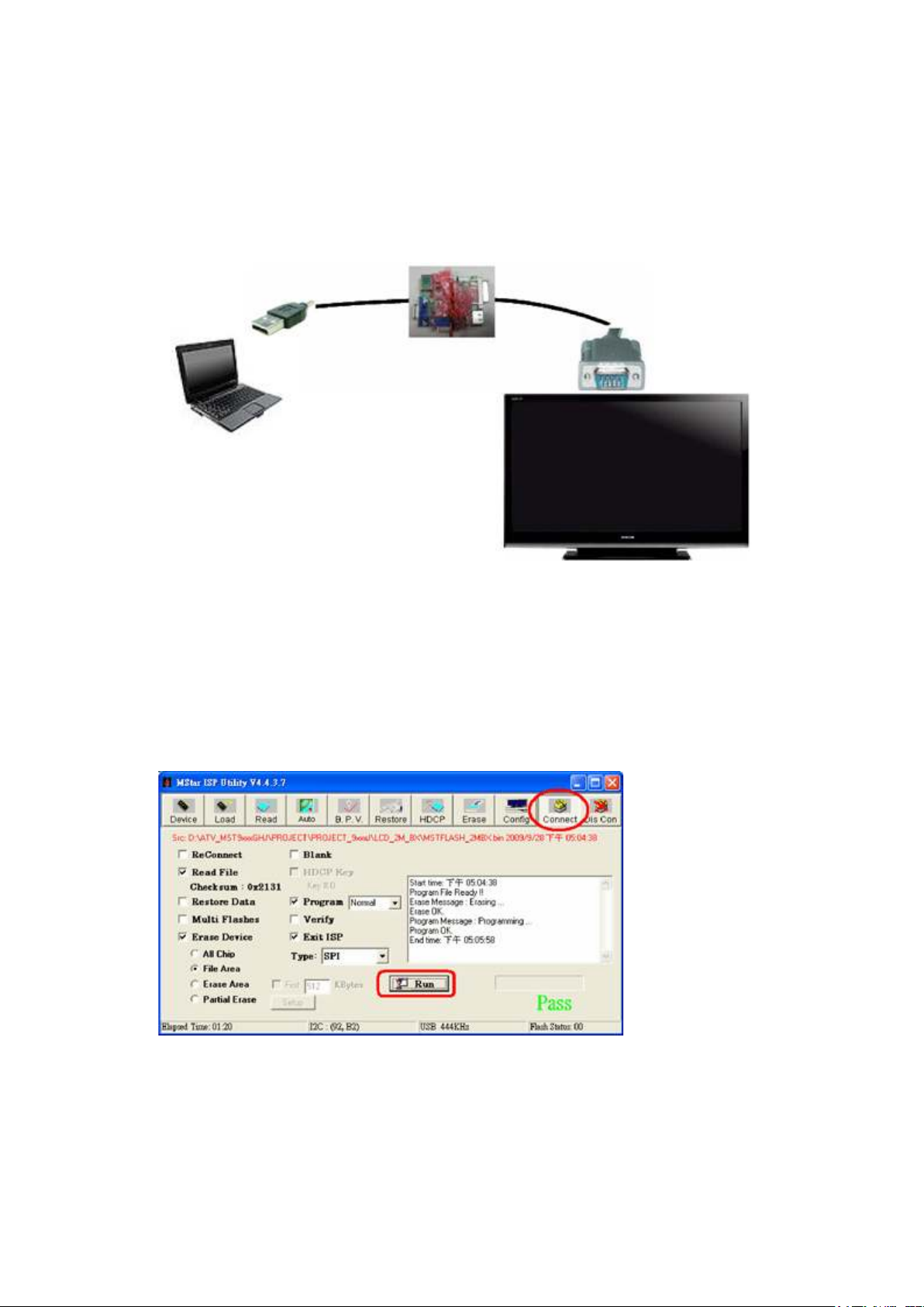
SOP of Firmware Upgrade
ATV Firmware Upgrade - Com port
Using USB to D-Sub 15 cable
1. COM Port and baud rate (9600 bps).
2. Select Read to load the file to be programmed into TV.
3. Push the button of Connect to connect TV and indentify the type of flash memory in
TV.
4. Push the Button of Run to start program firmware.
• Working method
◦ Unlike the USB upgrade (to be mentioned later) the whole code in flash memory
will be upgraded completely.
◦ This upgrade method can be done even the flash memory is blank.
ATV Firmware Upgrade - USB
Page 3
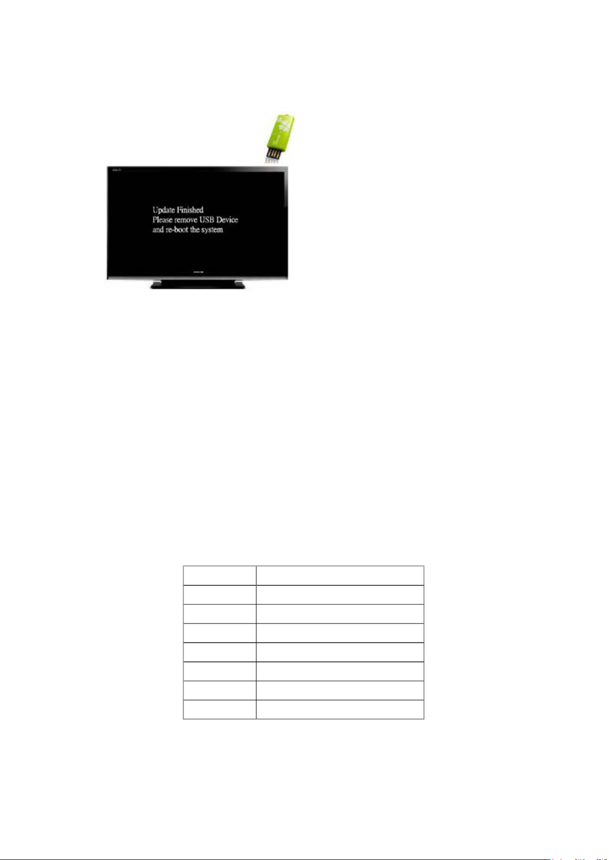
1.
Copy an available file (to be mentioned later) into USB memory disk.
2. Insert USB flash disk with an available file into TV USB port.
Стр. 2
из 3How to update using a USB Mass
-
storage device
16.
04.
2015
file:///C:/Users/
Александр
/
Desktop/32AV703R
-
01/html/!firmware.html
3. Reboot (AC Off/On) TV to update firmware automatically, during upgrading f/w a
progress slider bar will be shown on display.
4. Once f/w upgrade is finished, a message of "Update Finished" will be shown on
display.
5. Remove USB flash disk then turn AC Off/On to reboot TV, new f/w will be active.
Available file name
• In order to not upgrade firmware with incorrect code which is for other model, only the
bin filename consistent with the current upgraded model is considered available, i.e.
the model name located in first 8 characters of filename will be checked.
• The first found file with available file name will be applied for upgrade, so it is
recommended to keep only one available file for one model is flash disk.
• For example 19AV703X_XXX_REV01.BIN. the model name 19AV703X (in blue)
should match to current upgraded model and total length of file name should be 23
characters, characters in red is not cared.
Available file name, Continued
• Table 1. the file name of firmware for 703X series.
Model Name File Name of BIN Code
19AV703X 19AV703X_XXX_REVXX.BIN
22AV703X 22AV703X_XXX_REVXX.BIN
26AV703X 26AV703X_XXX_REVXX.BIN
32AV703X 32AV703X_XXX_REVXX.BIN
32LV703X 32LV703X_XXX_REVXX.BIN
37LV703X 37LV703X_XXX_REVXX.BIN
40LV703X 40LV703X_XXX_REVXX.BIN
Table 1. Firmware naming
• Internal Working Method
Page 4

◦
There are two part of codes in flash memory one is boot code the other one is
application code.
Стр. 3
из 3How to update using a USB Mass
-
storage device
16.
04.
2015
file:///C:/Users/
Александр
/
Desktop/32AV703R
-
01/html/!firmware.html
◦ At power up stage Boot code is first running up, it will check if there is USB
flash memory found.
◦ If USB flash memory is not found then the program will run to application code
which is the one designed for whole system control such as OSD, remote
control, display control etc.
• Internal Working Method, Continued
◦ If USB flash memory is found, boot code will check if any available file name
memory disk, if it is then the whole file with 2048K bytes (if it's a firmware) will
be copied to DDR memory first.
◦ After copy is finished, program jump to DDR and copy the part of new
application into flash memory on board.
◦ Once upgrade is done, program will keep waiting for reboot.
• Internal Working Method, Continued
◦ As boot code will not check any of checksum, care should be taken to avoid any
of invalid file with file name as Table 1. in USB flash memory while running
firmware upgrade process.
◦ As boot code and application code are running independently, after program runs
to application code the boot code is not able to be found by application code, so
it is not possible to implement USB upgrade directly from application code.
◦ This upgrade method can be done only when boot code is exist in flash memory.
Page 5
FUNCTION AND OPERATION
Стр. 1
из
6
16.
04.
2015
file:///C:/Users/
Александр
/Desktop/32AV703R
-
01/html/!func
-
ope.html
Front Key Controls
OSD operation for PC and TV OSD can be controlled by top control keypads or remote
control.
Function TV/video mode PC mode
POWER Turn off/on the set Turn off/on the set
"+" (CHANNEL) Menu Navigate Up/Channel up Menu Navigate Up
"–" (CHANNEL)
"+" (VOLUME)
"–" (VOLUME)
MENU Enter /Exit OSD menu Enter /Exit OSD menu
INPUT Source switch Source switch
• POWER key press will wake-up the TV set from 'Standby' mode.
• Navigate to and select function via CHANNEL "+ / –" keys, and VOLUME "+ / –"
keys. Then adjust using up/down functionality.
• Access main menu by pressing "MENU" key.
• Switch source by pressing "INPUT" key.
Menu Navigate Down/Channel
Down
Menu Navigate
Right/Increase/Volume up
Menu Navigate
Left/Decrease/Volume down
Menu Navigate Down
Menu Navigate
Right/Increase/Volume up
Menu Navigate
Left/Decrease/Volume down
LED Indicator
• LED1: (On/Off Control)
Normal ON: Green
Standby mode: Red
Switch OFF: No light
• LED2: (Timer Control)
Timer ON: Green
Timer OFF: No light
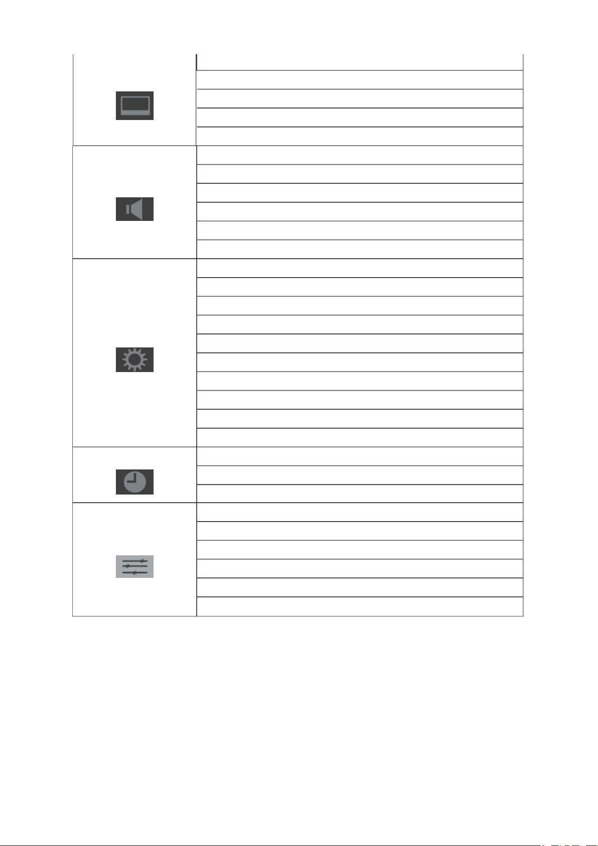
OSD Menu
To open the main menus (illustrated below), press MENU on the remote control or TV
control panel.
Picture Settings
Page 6
Picture
Active Backlight Control
Стр. 2
из
6
16.
04.
2015
file:///C:/Users/
Александр
/
Desktop/32AV703R
-
01/html/!func
-
ope.html
Sound
SET UP
3D Color management
Base Color adjustment
DNR
MPEG NR
Dual
Bass
Treble
Balance
Surround
Bass boost
Language
Country
Auto tuning
Manual tuning
AV connection
Quick Setup
Timer
Function
Remote Control
Picture Position
Automatic Power Down
Location
Reset TV
Sleep Timer
On timer
On timer position
Teletext
Panel lock
Auto format
4:3 stretch
Blue screen
Side panel
Page 7
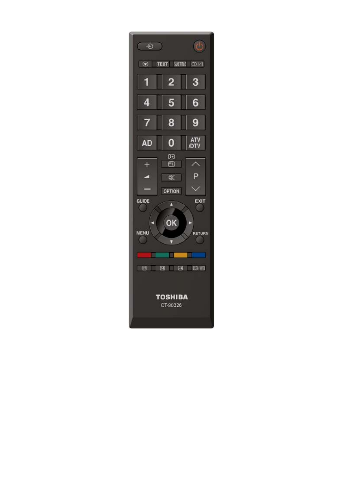
POWER: Press to turn on/off the TV from or to standby mode.
Стр. 3
из
6
16.
04.
2015
file:///C:/Users/
Александр
/
Desktop/32AV703R
-
01/html/!func
-
ope.html
VIDEO: 1. Press repeatedly to select the signal source.
STILL: Press to do freeze function
TEXT: Press to turn teletext mode ON/OFF (with MIX)
SUBTITLE: TTX subtitle
STEREO/DUAL: Press to select Mono / Stereo / DUAL from TV RF input.
Number Key: 1. Press number button to direct access to TV channel
2. The Source List should be activated and show on OSD
3. 1st press displays current, subsequent presses advance
2. Press the pass code to activate the factory mode
3. Press to activate the Channel Lock (enter PIN code for Channel
lock)
Page 8
4. If channel list OSD active - jump to that channel in the channel
list
Стр. 4
из
6
16.
04.
2015
file:///C:/Users/
Александр
/
Desktop/32AV703R
-
01/html/!func
-
ope.html
AD: N/A
ATV/DTV: N/A
VOL +/ –: Press to adjust the volume
I+/ INDEX: info display / TTX index
MUTE: Press to Interrupt the sound or restore it.
OPTION: Go to shortcut menu
P / : 1. Press to browse channels
2. The channel number should appear on the set
GUIDE: N/A
EXIT: Press to Exit OSD
Cursor Key: 1. Press cursor up/button to navigate OSD menu item
2. Cursor right key perform confirmation as well as proceed next
level of OSD
3. Can use cursor left to return previous level
MENU: Press to activate OSD menu and back to previous level of OSD
RETURN: Press to return previous level
OK Key: OK
Red Key: TTX Red button
Green Key: TTX Green button
Yellow Key: TTX Yellow button
Cyan: TTX Cyan button
REVEAL: TTX Reveal button
HOLD: TTX Hold button
FULL-TOP-BOTTOM: TTX zoom
TIME / TXCL: Time display / TTX cancel
• Remote Control active area:
Angle Distance
0 º (for H & V) ≥ 5 m
30 º (for H & V) ≥ 5 m
I/O connectors
Rear connectors:
Page 9
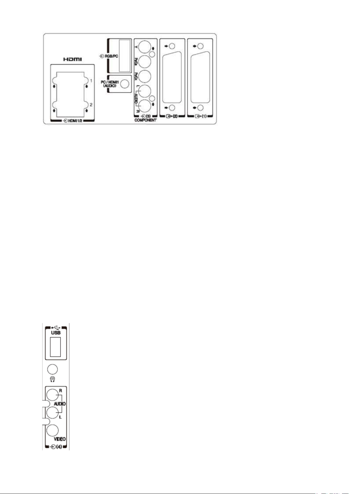
Tuner input:
Стр. 5
из
6
16.
04.
2015
file:///C:/Users/
Александр
/
Desktop/32AV703R
-
01/html/!func
-
ope.html
RF connector for PAL/SECAM/NTSC 4.43 free air and cable reception.
HDMI 1/2 input:
Including digital video and audio. HDMI and PC mode share PC audio when system checks
no audio header.
SCART 1 input:
Including RGB in, CVBS in TV out.
SCART 2 input:
Half SCART includes S-Video in, CVBS in and audio L/R in, TV out.
Component input:
YPbPr is with R/L audio in.
HDMI/PC Audio input:
3.5 φ mini-jack
PC VGA input:
D-SUB 15 pin with RS232 function.
Side connectors
Page 10

Headphone output:
3.5 φ mini-jack
Стр. 6
из
6
16.
04.
2015
file:///C:/Users/
Александр
/
Desktop/32AV703R
-
01/html/!func
-
ope.html
Side AV input:
CVBS with R/L audio in
USB:
Software upgrade
Page 11
SAFETY INSTRUCTION
Стр. 1
из 3Handling the LCD Module
16.
04.
2015
file:///C:/Users/
Александр
/Desktop/32AV703R
-
01/html/!handling_lcd.html
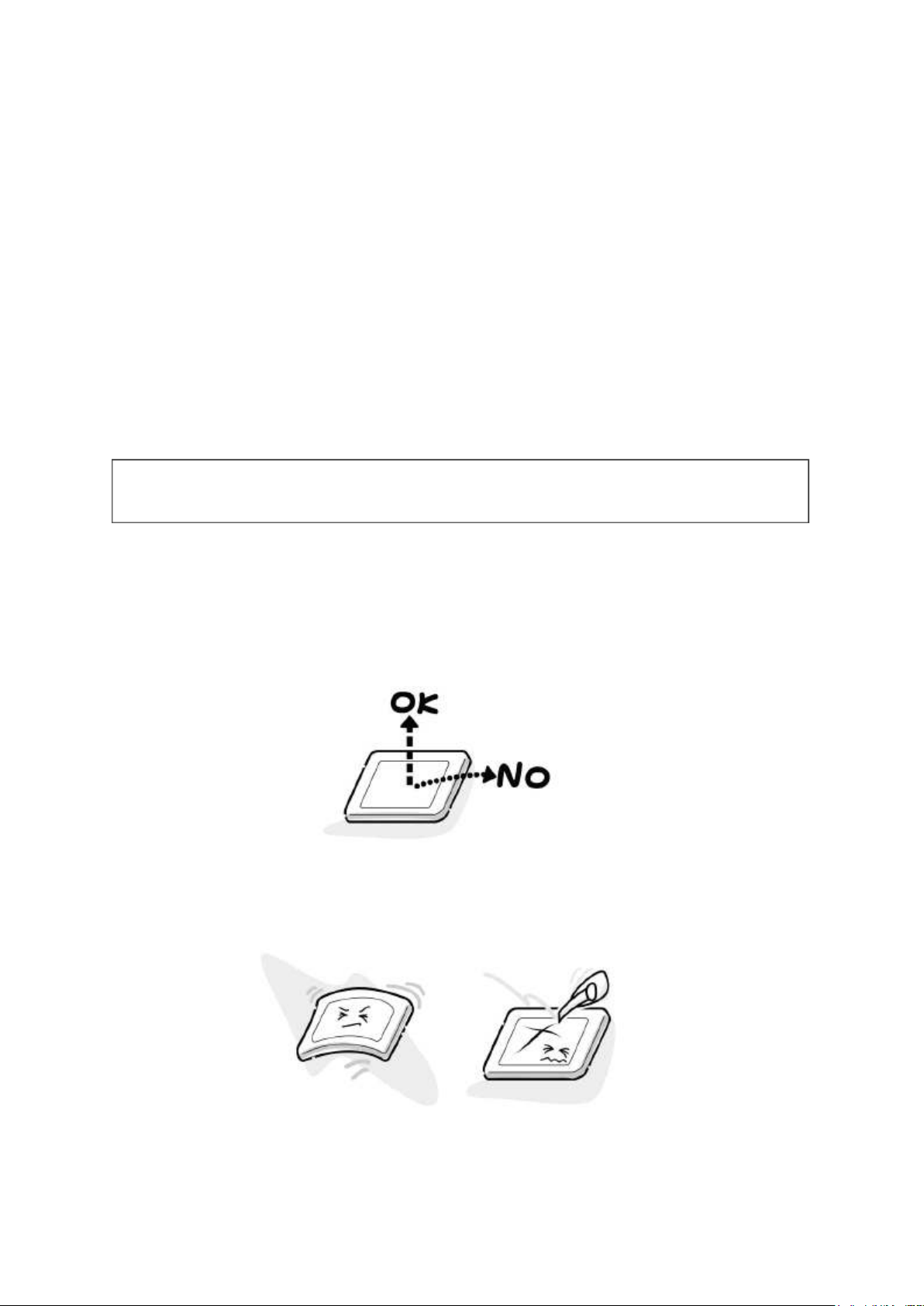
Handling the LCD Module
Safety Precaution
In the event that the screen is damaged or the liquid crystal (fluid) leaks, do not breathe in or
drink this fluid.
Also, never touch this fluid. Such actions could cause toxicity or skin irritation. If this fluid
should enter the mouth, rinse the mouth thoroughly with water. If the fluid should contact the
skin or clothing, wipe off with alcohol, etc., and rinse thoroughly with water. If the fluid
should enter the eyes, immediately rinse the eyes thoroughly with running water.
Precautions for Handling the LCD Module
CAUTION: The metal edges of the LCD module are sharp, handle it with
care.
The LCD module can easily be damaged during disassembly or reassembly; therefore,
always observe the following precautions when handling the module.
1. When attaching the LCD module to the LCD cover, position it appropriately and fasten
at the position where the display can be viewed most conveniently.
2. Carefully align the holes at all four corners of the LCD module with the corresponding
holes in the LCD cover and fasten with screws. Do not strongly push on the module
because any impact can adversely affect the performance. Also use caution when
handling the polarized screen because it can easily be damaged.
3. If the panel surface becomes soiled, wipe with cotton or a soft cloth. If this does not
remove the soiling, breathe on the surface and then wipe again.
If the panel surface is extremely solied, use a CRT cleaner as a cleaner. Wipe off the
panel surface by drop the cleaner on the cloth. Do not drop the cleaner on the panel.
Page 12
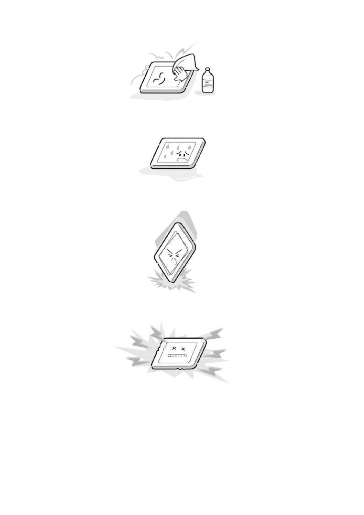
Pay attention not to scratch the panel surface.
4. Leaving water or other fluids on the panel screen for an extended period of time can
Стр. 2
из 3Handling the LCD Module
16.
04.
2015
file:///C:/Users/
Александр
/
Desktop/32AV703R
-
01/html/!handling_lcd.html
result in discoloration or stripes. Immediately remove any type of fluid from the
screen.
5. Glass is used in the panel, so do not drop or strike with hard objects. Such actions can
damage the panel.
6. CMOS-LSI circuitry is used in the LCD module, so avoid damage due to static
electricity. When handling the module, use a wrist ground or anchor ground.
7. Do not expose the LCD module to direct sunlight or strong ultraviolet rays for an
extended period of time.
Page 13
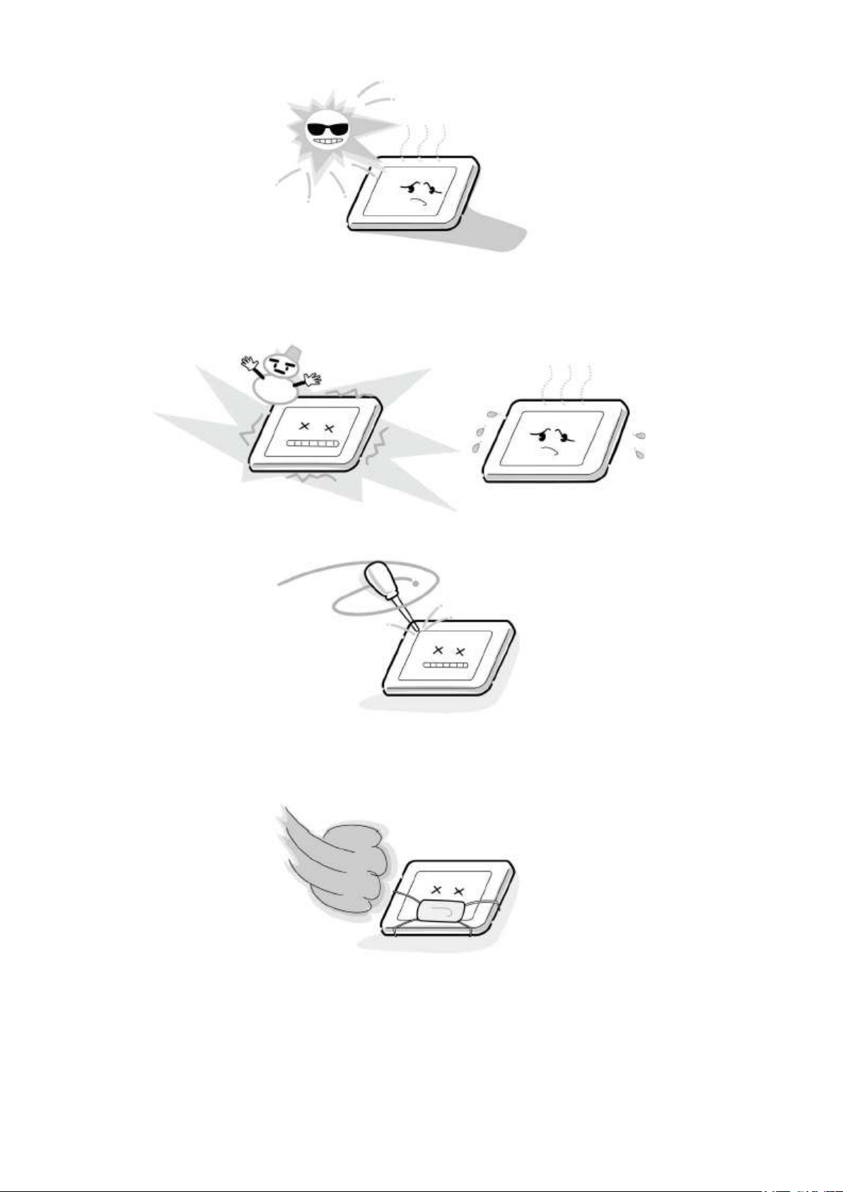
8. Do not store the LCD module below the temperature conditions described in the
Стр. 3
из 3Handling the LCD Module
16.
04.
2015
file:///C:/Users/
Александр
/
Desktop/32AV703R
-
01/html/!handling_lcd.html
specifications. Failure to do so could result in freezing of the liquid crystal due to cold
air or loss of resilience or other damage.
9. Do not disassemble the LCD module. Such actions could result in improper operation.
10. When transporting the LCD module, do not use packing containing epoxy resin
(amine) or silicon resin (alcohol or oxim). The gas generated by these materials can
cause loss of polarity.
Page 14

INSTALLATION
Стр. 1
из
3
16.
04.
2015
file:///C:/Users/
Александр
/Desktop/32AV703R
-
01/html/!installation.html
Channel Settings
Initial setup
The first time user switches on TV set, "initial setup" wizard will be shown in OSD menu to
guide user to start channel scanning. The "channel scanning" takes several minutes. To stop
the scanning, press the "EXIT" key.
1. Select your language
2. Select your country
3. Start scanning
"Channel scanning", "Analog channels: found channel no." and status will be shown in
OSD menu during scanning.
Channel scan (on TV mode)
1. Select "country": Press "MENU" on the remote control. Then select "Set up" →
"Country" → your country in OSD.
2. Start scanning: Press "MENU" on the remote control. Then select "Set up" → "Auto
tuning" to start scanning.
When channel scanning finished, press "EXIT" key to leave OSD menu.
The found analog programs will be numbered in ascending order starting from 0.
Analog manual store
Press "MENU" on the remote control. Then select "Set up" → "Manual tuning" to start
manual scanning from user specified frequency. Once new program is found, user can store
this new program to a new program number.
Channel skip
1. Press "MENU" on the remote control. Then select "Set up" → "Manual tuning", then
follow OSD indication to select Channel skip.
2. Use up / down key to select the program you want to skip. Then press "OK" key. A
"tick" symbol will be show in right side box.
3. Press "EXIT" to leave OSD menu.
The skipped program number will not be found by pressing CH +/– key.
Channel sort
It will be automatically sorted after auto tuning.
Channel name edit
Press "MENU" on the remote control. Then select "Set up" → "Manual tuning", then follow
OSD indication to edit channel name.
Page 15

Hotel Mode
Стр. 2
из
3
16.
04.
2015
file:///C:/Users/
Александр
/
Desktop/32AV703R
-
01/html/!installation.html
Enter Hotel Mode
1. Press "MUTE" button on the remote, and display [mute].
2. Within 2 sec, press "MUTE" button on the remote again, and hold the button down for
3 sec.
3. Then, press "INPUT" button on the TV side. Then hotel mode menu will appear.
Exit Hotel mode
Turn the TV power off
Hotel Mode Function
# Function
0 Hotel Mode On/Off Hotel Mode Off Hotel Mode On
1 Panel Lock
Disable TV Front/Side
buttons
2 Panel Lock W/O input
selector keys.
Disable TV Front/Side
buttons except for input
selector keys
3 Disable remote control
(In Service Mode, not
disabled)
4 Disable Setup Menu Setup menu is
Settings *off
(normal setting)
All keys work
normally.
All keys work
normally.
Remote control works
normally.
normally displayed.
Settings on
Disabled
Disabled except for input selector
keys.
Disabled remote control.
Setup menu is disabled.
5 Setup Menu W/O Lang.
Disable set up menu except
for language setting.
*Only language setting is
available in Setup menu.
6 Max volume setting
(Setting Method: Set 100
volume, then turning and
choice this value)
7
Setup menu is
normally displayed.
00~100 [dec] (normal:
100)
only language setting is displayed
at setup menu.
Page 16

Fixed Pos/Video
Turn the TV on by power
on: fixed pos/video set
Стр. 3
из
3
16.
04.
2015
file:///C:/Users/
Александр
/
Desktop/32AV703R
-
01/html/!installation.html
button on the remote, then
display goes to fixed
POS/Video
TV, Component, AV, ... , PC,
HDMI, .... Off
TV: 1~255 [dec] (normal: 0)
8 Fixed Volume
Turn the TV on by power
button on the remote, then
volume is set to the forced
value.
9 Fixed Picture Mode
Turn the TV on by power
button on the remote, then
the fixed picture mode is
selected.
10 Welcome message
Turn the TV on by power
button on the remote, then a
message ("Welcome to our
hotel") is displayed.
on:: fixed vol. set
0~100 [dec] (normal: 0)
*101~: not available
on: Fixed Picture Mode.
0: Dynamic selected
1: Standard
2: Mild
3: Movie
4: User (Default)
On (Enable)
1: 8sec
2: 15sec
3: until first operation
(Until next operation (ex. Ch up)
the message remains.)
11 TV to USB
Save the data of TV
settings to USB memory
(includes user setting, the
setting of hotel mode and
channel table).
12 USB to TV
Load the data of TV
settings in USB memory to
TV (includes user setting,
the setting of hotel mode
and channel table).
Page 17

ˠ˴˼ʳ˕˴˷ˣ˸ʳ˕˴˷
˜˸˸
˕˴˷
˞˸˴˷
˕˴˷
˜˥˂˟˘˗ʳ˕˴˷
˧˖ˢˡʳ˕˴˷
Page 18

SAFETY INSTRUCTION
Стр. 1
из
3
16.
04.
2015
file:///C:/Users/
Александр
/
Desktop/32AV703R
-
01/html/!safe[lcd]asia_eu.html
WARNING: BEFORE SERVICING THIS CHASSIS, READ THE "SAFETY PRECAUTION" AND
"PRODUCT SAFETY NOTICE" INSTRUCTIONS BELOW.
Safety Precaution
WARNING: SERVICING SHOULD NOT BE ATTEMPTED BY ANYONE UNFAMILIAR WITH THE
NECESSARY PRECAUTIONS ON THIS RECEIVER. THE FOLLOWING ARE THE NECESSARY
PRECAUTIONS TO BE OBSERVED BEFORE SERVICING THIS CHASSIS.
1. An isolation transformer should be connected in the power line between the receiver and the AC line before any
service is performed on the receiver.
2. Always disconnect the power plug before any disassembling of the product. It may result in electrical shock.
3. When replacing a chassis in the cabinet, always be certain that all the protective devices are put back in place, such
as nonmetallic control knobs, insulating covers, shields, isolation resistor-capacitor network, etc.
4. Always keep tools, components of the product, etc away from the children, These items may cause injury to
children.
5. Depending on the model, use an isolation transformer or wear suitable gloves when servicing with the power on,
and disconnect the power plug to avoid electrical shock when replacing parts. In some cases, alternating current is
also impressed in the chassis, so electrical shock is possible if the chassis is contacted with the power on.
6. Always use the replacement parts specified for the particular model when making repairs. The parts used in
products require special safety characteristics such as inflammability, voltage resistance, etc. therefore, use only
replacement parts that have these same characteristics. Use only the specified parts when the mark is indicated
in the circuit diagram or parts list.
7. Parts mounting and routing dressing of wirings should be the same as that used originally. For safety purposes,
insulating materials such as isolation tube or tape are sometimes used and printed circuit boards are sometimes
mounted floating. Also make sure that wirings is routed and clamped to avoid parts that generate heat and which
use high voltage. Always follow the manufactured wiring routes / dressings.
8. Always ensure that all internal wirings are in accordance before re-assembling the external casing after a repairing
completed. Do not allow internal wiring to be pinched by cabinets, panels, etc. Any error in reassembly or wiring
can result in electrical leakage, flame, etc., and may be hazardous.
9. NEVER remodel the product in any way. Remodeling can result in improper operation, malfunction, or electrical
leakage and flame, which may be hazardous.
10. Touch current check. (After completing the work, measure touch current to prevent an electric shock.)
• Plug the AC cord directly into the AC outlet. Do NOT use an isolation transformer for
this check.
• Connect a measuring network for touch currents between each exposed metallic part on
the set and a good earth ground such as a water pipe.
Annex D
(normative)
Measuring network for TOUCH CURRENTS
Page 19

Resistance values in orms (Ω).
Стр. 2
из
3
16.
04.
2015
file:///C:/Users/
Александр
/
Desktop/32AV703R
-
01/html/!safe[lcd]asia_eu.html
V: Voltmeter or oscilloscope
(r.m.s. or peak reading)
Input
resistance :
1 MΩ
Input
capacitance :
200 pF
Frequency
range : 15
Hz to 1
MHz and
d.c.
respectively
Note: Appropriate measures should be taken to obtain the correct value in case of non
sinusoidal waveforms.
The measuring instrument is calibrated by comparing the frequency factor of with the solid
line in figure F.2 of IEC 60990 at various frequencies. A calibration curve is constructed
showing the deviation of from the ideal curve as a function of frequency.
TOUCH CURRENT = /500 (peak value).
• The potential at any point (TOUCH CURRENT) expressed as voltage and does not
exceed the following value:
The part or contact of a TERMINAL is not HAZARDOUS LIVE if:
a) The open-circuit voltage should not exceed 35 V (peak) a.c. or 60 V d.c. or, if a) is
not met.
b) The measurement of the TOUCH CURRENT shall be carried out in accordance
with IEC 60990, with the measuring network described in Annex D of this
standard.
The TOUCH CURRENT expressed as voltages and , does not exceed the
following values:
- for a.c. : = 35 V (peak) and = 0.35 V (peak);
- for d.c. : = 1.0 V
Note: The limit values of = 0.35 V (peak) for a.c. and = 1.0 V for d.c. correspond to the
values 0.7 mA (peak) a.c. and 2.0 mA d.c.
Product Safety Notice
Many electrical and mechanical parts in this chassis have special safety-related characteristics. These characteristics are
often passed unnoticed by a visual inspection and the protection afforded by them cannot necessarily be obtained by
using replacement components rated for higher voltage, wattage, etc. Replacement parts which have these special safety
characteristics are identified in this manual and its supplements; electrical components having such features are
Page 20

identified by the international hazard symbols on the schematic diagram and the parts list.
Before replacing any of these components, read the parts list in this manual carefully. The use of substitute replacement
Стр. 3
из
3
16.
04.
2015
file:///C:/Users/
Александр
/
Desktop/32AV703R
-
01/html/!safe[lcd]asia_eu.html
parts which do not have the same safety characteristics as specified in the parts list may create electrical shock, fire, or
other hazards.
Page 21

SPECIFICATION
Стр. 1
из
3
16.
04.
2015
file:///C:/Users/
Александр
/Desktop/32AV703R
-
01/html/!spec.html
Electrical
LCD
Samsung 32 inch panel:
Panel Model: LTA320AP08
Active Area: 697.685 mm (H) × 392.256 mm (V)
Outline Dimension: 760.0 mm (H) × 450.0 mm (V) × 50.2 mm (D)
Pixel Pitch: 0.51075 mm (H) × 0.51075 mm (V)
Pixel Format: 1366 × 768 (WXGA), RGB strip arrangement
Color Depth: 8-bit, 16.7M colors
Luminance:
Backlight: 4 U-type CCFL
Response Time: 8.0 msec. (G to G average)
Viewing Angle: 178/ 178 (L/R, U/D) (CR ≥ 10)
Contrast Ratio: 4000:1 (Typ.)
Life Time: 50,000 hrs
> 400 cd/m2 (Min), 450 cd/m2 (Typ.)
Power supply
Features
AC line voltage range: 200 Vac ~ 264 Vac
AC line frequency range: 47 ~ 63 Hz
Power consumption
Normal on: < 100 W (LTA320AP08)
Max Current: < 0.5 A (LTA320AP08)
Standby: < 1 W at 230 Vac/50 Hz mains, standby mode
Video / Audio signals
TV / AV signal
TV RF input system: PAL/SECAM/NTSC 4.43
CVBS input: 1.0 Vpp (including 300 mV sync level), 75 Ω
Component video input: Y: 1.0 Vpp (include sync), PbPr: 700 mVpp, 75 Ω .
Support 480i/p, 576i/p, 720p, 1080i at 50/60 Hz refresh
rate.
Audio input: 2.0 V max, > 10 k Ω.
SCART input / output: SCART 1 includes RGB in, CVBS in, TV out.
SCART 2 includes S-Video in, CVBS in and audio L/R
in, TV out.
HDMI (High Definition Multimedia Interface)
Support 480i /480p, 576i/576p, 720p, 1080i, 1080p
(24/25/50/60 Hz) format with HDCP.
Page 22
Digital interface with 4 channels TMDS signal.
Audio Lips synchronization.
Стр. 2
из
3
16.
04.
2015
file:///C:/Users/
Александр
/
Desktop/32AV703R
-
01/html/!spec.html
HDMI/PC Audio input: 500 mVrms. > 10 k Ω
Headphone output: 15 mW (Typ.) at 32 ohm, 8~600 ohm.
Amplifier output: 10W × 2 @ T.H.D.< 10 %
Mechanical
Unit dimension (without Base): 798.22 mm (W) × 88 mm (D) × 516 mm (H)
Unit dimension (with Base): 798.22 mm (W) × 233 mm (D) × 563.54 mm (H)
Net Weight: 12 Kg
Gross Weight: 16 Kg
Picture
Picture in TV / Video modes
There are 5 pre-settings: Dynamic / Standard / Mild / Movie / User
Pre-settings -
Picture mode Dynamic Standard Mild Movie User
Backlight 100 70 50 30 50
Contrast 100 95 90 90 95
Brightness 50 50 50 50 50
Color 50 50 50 50 50
Tint 0 0 0 0 0
Sharpness 50 50 50 50 50
Black/White level High Middle Low Middle Low
Picture Size
• There are 7 picture formats: Wide, 4:3, Super Live, Cinema, Subtitle, 14:9 and Native
(HDMI only) mode.
Note: 1. Panorama format is only available for 480i or 576i video mode.
2. Automatic format is only activated for ATV signal with WSS information.
Dimming Backlight
Dimming range: Min: 0 V, Max: 5V
Control by the detection of TV controller's histogram via external PWM
Burst dimming voltage DC 0.0V ~ 3.3V
Page 23
Audio
Стр. 3
из
3
16.
04.
2015
file:///C:/Users/
Александр
/
Desktop/32AV703R
-
01/html/!spec.html
For the sake of stereo, proper segment of R/L speakers is needed to make sure correct R/L
channel separation.
No Item Min Typ Max Unit Remark
1 Audio Output RF Audio Output
(RF input 1 kHz 54 % modulation
(around 0.9 Vrms) / EQ Off / Distortion
10 %)
AV Audio Output
(1 KHz 0.5 Vrms Input / EQ Off /
Distortion 10 %)
2 Speaker
Impedance
Earphone 32 ohm
Speaker 6 ohm
9 10 11 W 6 ohm
9 10 11 W 6 ohm
Others
• AV reset items include ... Picture and Audio back to factory setting
• Sleep timer: OFF, 10min, 20min, 30min, 40min, 50min, 60min, 90min, 120min
• TELETEXT (100 pages)
◦ TELETEXT ON/OFF
◦ SUBPAGE
◦ INDEX
◦ SUBTITLE
◦ HOLD (Stop acquisition)
◦ REVEAL (Show hidden information)
◦ TELETEXT MIX
◦ TELETEXT ZOOM
Page 24
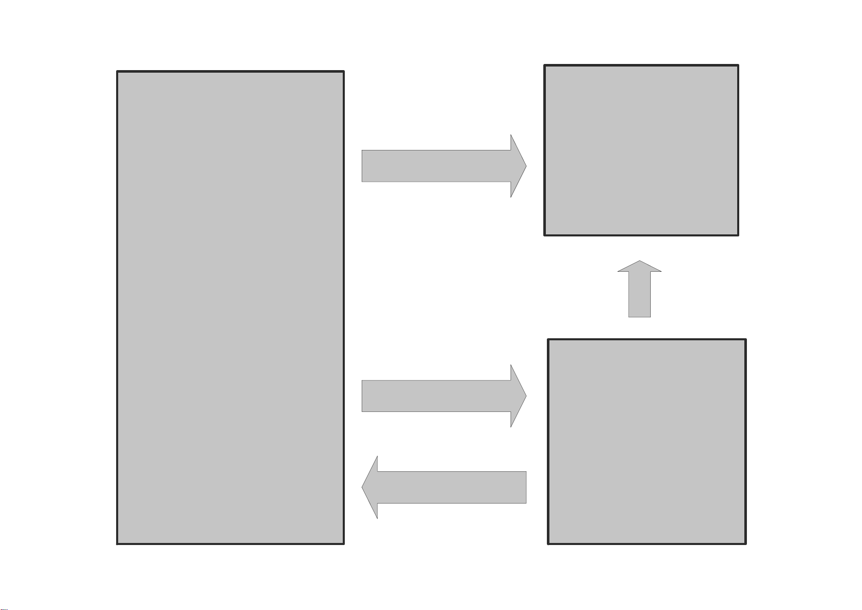
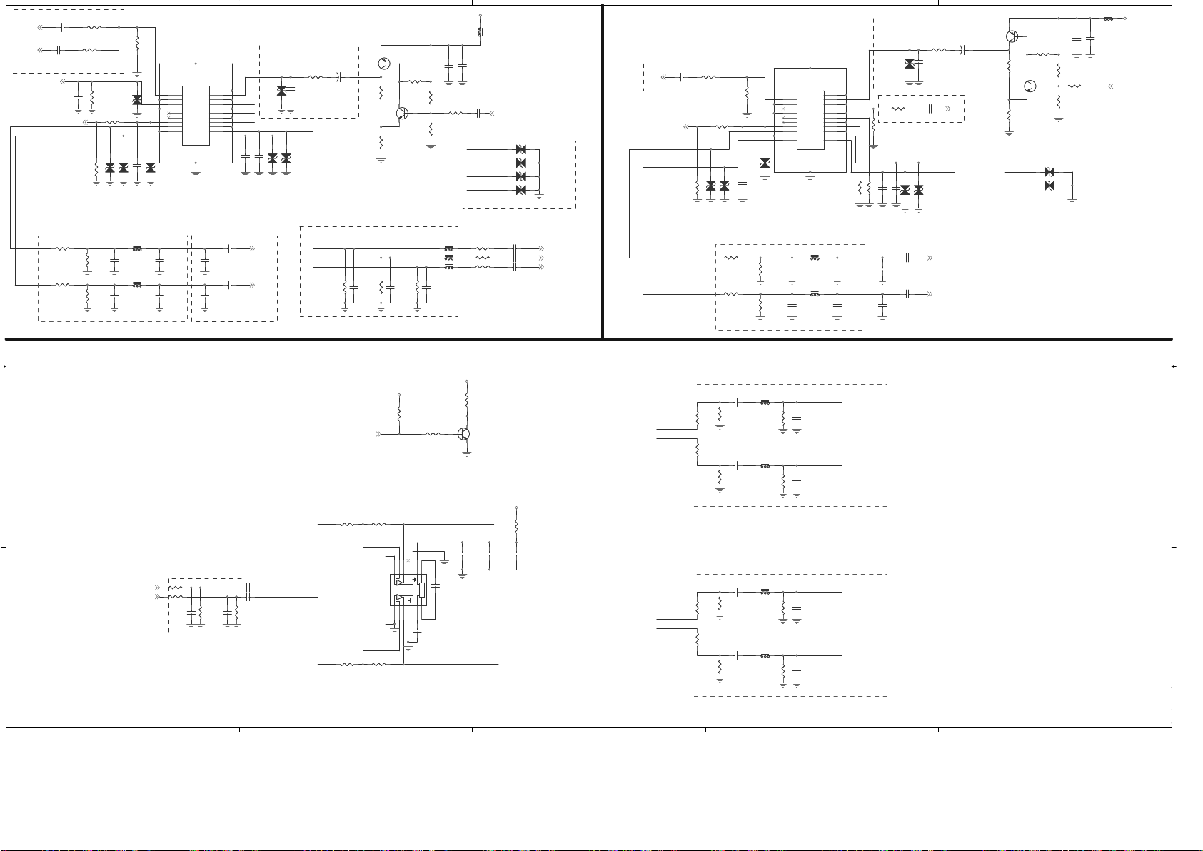
Main BD
Power BD
Panel
+5V +12V
ACD
PS_ON
Diming
BL_ON
LVDS out
+24V
Diming
BL_ON
Page 25
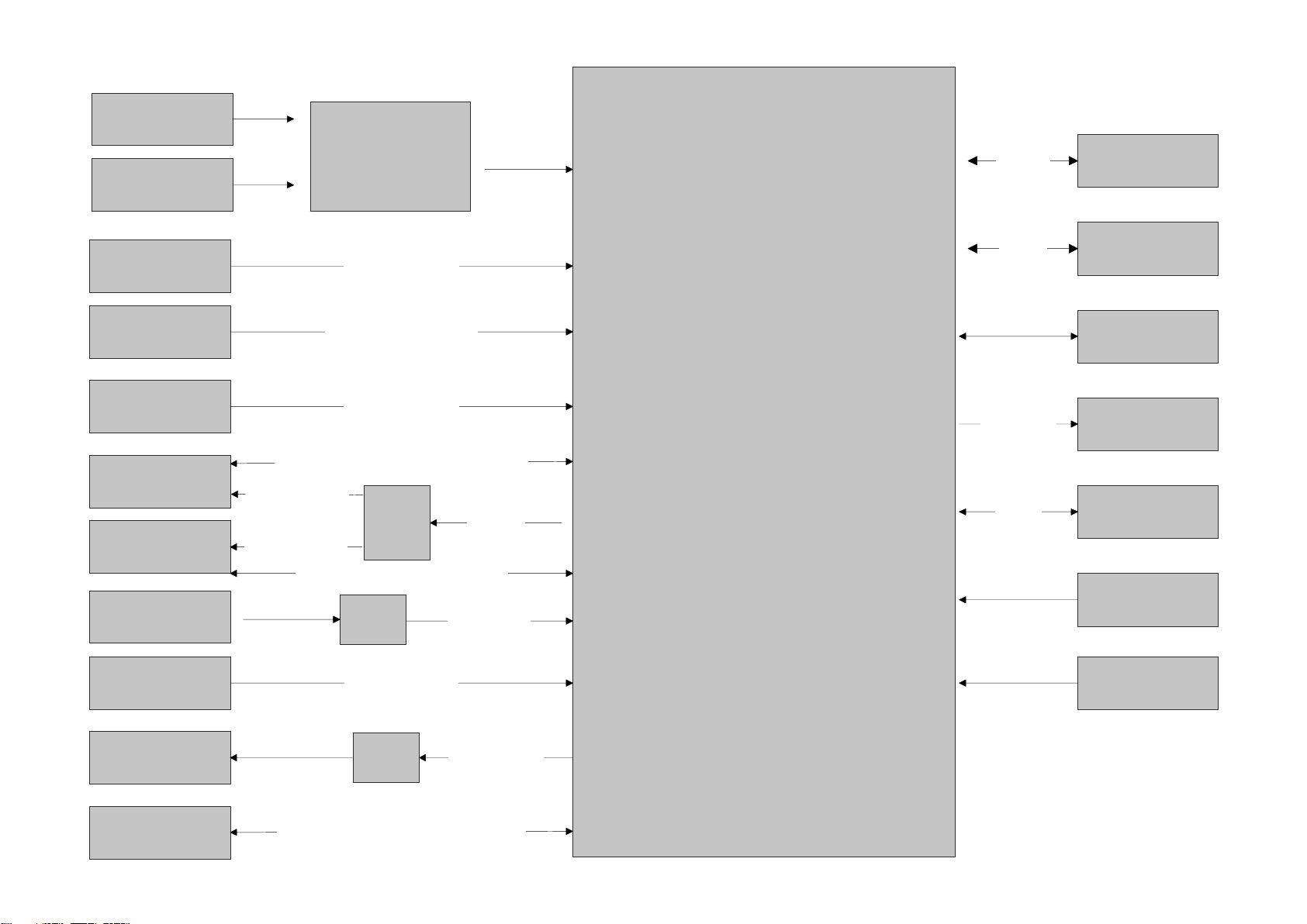
MST9B884J
HDMI 1
HDMI 2
HDMI Switch
R/G/B/H/V/DDC Bus
VGA
Phone Jack
Component
+L/Mono-R
SCART 1
Tuner
AV+L/Mono-
R (Side)
Phone Jack
(Side)
USB (Side)
VGA & HDMI 1 Audio Input
YPbPr + Audio Input
VIF / SIF Input
CVBS + Audio Input
F/W
U
p
gra
de,
J
PEGView
e
r
andMP3Playe
r
Audio Out
SAW
Filter
SCA
R
T
A
u
dio
O
u
t
DDR 16MB
SPI Flash
2MB
NVRAM
PANEL
Audio AMP
Keypad
IR
DDR Bus
SPI Bus
I2S Bus
LVDS Output
SCART 2
SCART AV, SV, Audio Input & TV Out
SCART Audio Out
Head Phone Out
AMP
TPA6132
SCART
R/G/B,A
V
,
SV,Au
dio
I
npu
t
&TV
Out
AMP
DRV602
Page 26

IR [Top]
Page 27

KEY [Top]
Page 28

MAIN [Bottom]
Page 29

MAIN [Top]
Page 30

POWER [Bottom]
Page 31

POWER [Top]
Page 32

5
5
4
4
3
3
2
2
1
1
D D
C C
B B
A A
RC_IR
LED_ON_OFF
LED_TIMER
LED_TIMER
LED_ON_OFF
RC_IR
+5V_STBY
+5V_STBY
+5V_STBY
+5V_STBY
+5V_STBY
LED
LED 1
LED 2
Function
Control
method
Standby Power on Timer
HW Power_on LED_Timer
Green GreenRed
IR
B
C
E
1
2
3
Q202
PMBS3904
B
C
E
1
2
3
Q202
PMBS3904
12
R208
10KOhm
R208
10KOhm
R204
1.5KOhm
R204
1.5KOhm
12
+
LED1
GREEN
+
LED1
GREEN
1
1
2
2
3
3
4
4
5
5
6
6
SIDE1
7
SIDE2
8
CN202
WtoB_CON_6P
CN202
WtoB_CON_6P
1
H5
C138D138N
H5
C138D138N
12
C204
1UF/10V
C204
1UF/10V
1 2
R209
0OHM
R209
0OHM
1 2
R201
10KOhm
R201
10KOhm
B
C
E
1
2
3
Q204
PMBS3904
B
C
E
1
2
3
Q204
PMBS3904
12
C203
0.01UF/50V
C203
0.01UF/50V
12
R206
10KOhm
R206
10KOhm
1
2
3
RED
GREEN
LED2
RED&GREEN
RED
GREEN
LED2
RED&GREEN
VCC
3
GND
2
OUT
1
NP_NC
4
U201
IRM-3638N3S13F4-P
U201
IRM-3638N3S13F4-P
12
D1 TVM1G180M120R/NCD1 TVM1G180M120R/NC
12
C201 0.1UF/16VC201 0.1UF/16V
R203
6.8KOhm
R203
6.8KOhm
12
C206 0.1UF/16V/NCC206 0.1UF/16V/NC
1 2
R210
1KOhm
R210
1KOhm
B
C
E
1
2
3
Q201
PMBS3904
B
C
E
1
2
3
Q201
PMBS3904
12
C205 0.1UF/16V/NCC205 0.1UF/16V/NC
1 2
R202
100Ohm
R202
100Ohm
B
C
E
1
2
3
Q203
PMBS3904
B
C
E
1
2
3
Q203
PMBS3904
R205
1.2KOhm
R205
1.2KOhm
12
C202 0.1UF/16V/NCC202 0.1UF/16V/NC
1
H4
C138D138N
H4
C138D138N
12
R207
10KOhm
R207
10KOhm
IR [1] IR & LED
Page 33

5
5
4
4
3
3
2
2
1
1
D D
C C
B B
A A
KEY2
KEY1
SOURCE
1.04V
MENU VOL-
0.35V1.73V
VOL+
POWERCH-
2.44V 1.73V 1.04V
CH+
2.44V
1 2
R105 4.3KOhmR105 4.3KOhm
1
H3
C138D138N
H3
C138D138N
1 2
R106
1.3KOhm
R106
1.3KOhm
1
T2T2
1
1
334
4
2
2
SW106
TACT_SW_4P
SW106
TACT_SW_4P
12
C102 0.1UF/16VC102 0.1UF/16V
1 2
R101 11KOhmR101 11KOhm
1
1
334
4
2
2
SW103
TACT_SW_4P
SW103
TACT_SW_4P
12
C104 0.1UF/16VC104 0.1UF/16V
12
C103 0.1UF/16VC103 0.1UF/16V
1 2
R102 4.3KOhmR102 4.3KOhm
1
H1
C138D138N
H1
C138D138N
12
C106 0.1UF/16VC106 0.1UF/16V
1
1
334
4
2
2
SW107
TACT_SW_4P
SW107
TACT_SW_4P
12
C101 0.1UF/16VC101 0.1UF/16V
1
1
2
2
3
3
4
4
SIDE1
5
SIDE2
6
CON1
WTOB_CON_4P
CON1
WTOB_CON_4P
12
C107 0.1UF/16VC107 0.1UF/16V
1
T3T3
1
1
334
4
2
2
SW102
TACT_SW_4P
SW102
TACT_SW_4P
1
H2
C138D138N
H2
C138D138N
12
C108 0.1UF/16VC108 0.1UF/16V
1
1
334
4
2
2
SW105
TACT_SW_4P
SW105
TACT_SW_4P
12
C109 0.1UF/16VC109 0.1UF/16V
1 2
R103
1.3KOhm
R103
1.3KOhm
12
C105 0.1UF/16VC105 0.1UF/16V
1
T1T1
1
1
334
4
2
2
SW104
TACT_SW_4P
SW104
TACT_SW_4P
1 2
R104 11KOhmR104 11KOhm
1 2
R107
470Ohm
R107
470Ohm
1
1
334
4
2
2
SW101
TACT_SW_4P
SW101
TACT_SW_4P
KEY [1] KEYPAD
Page 34
5
5
4
4
3
3
2
2
1
1
D D
C C
B B
A A
B
G
DDCSCL
DDCSDA
R
HS
VGA_5V
VS
DSUB_11
DSUB_4
DSUB_11
DSUB_4
PC_AU_INR
PC_AU_INL
R
G
B
VGA5V
VGA5V
+5V_SW
HS_RGB 7
VS_RGB 7
RIN+ 7
GIN+ 7
BIN+ 7
SOG 7
ISP2_SCL 7
ISP2_SDA 7
DDC_DSUB_WP 5
AUL5 2
AUR5 2
VGA Phone Jack
Close to Connector
Close to IC
12
C101810PF/50VNC C101810PF/50VNC
12
ZD1004ADUC10S03005NCZD1004ADUC10S03005
NC
12
ZD1007
PESD0603-240
NC
ZD1007
PESD0603-240
NC
12
C101910PF/50VNC C101910PF/50VNC
R1013 47OhmR1013 47Ohm
R1017
75OHM
R1017
75OHM
R1007
4.7KOhm
R1007
4.7KOhm
21
FB1001 120Ohm/100MhzFB1001 120Ohm/100Mhz
12
C1013 1000PF/50VC1013 1000PF/50V
1 2
R1018 470OhmR1018 470Ohm
1 2
C1014
0.1UF/16V
C1014
0.1UF/16V
12
ZD1003ADUC10S03005NCZD1003ADUC10S03005
NC
12
D1002ADUC10S03005NCD1002ADUC10S03005
NC
12
ZD1005ADUC10S03005NCZD1005ADUC10S03005
NC
12
C1006
22PF/50V
C1006
22PF/50V
R112812KOhm R112812KOhm
R10282.2KOHM R10282.2KOHM
12
C1001
0.1UF/16V
C1001
0.1UF/16V
R1008
4.7KOhm
R1008
4.7KOhm
R10272.2KOHM R10272.2KOHM12C102210PF/50VNC C102210PF/50VNC
12
C102010PF/50VNC C102010PF/50VNC
R1026 100OhmR1026 100Ohm
12
C1012 47NF/25VC1012 47NF/25V
12
ZD1002ADUC10S03005NCZD1002ADUC10S03005
NC
R1019
75OHM
R1019
75OHM
1
1
3
3
NP_NC2
5
2
2
NP_NC1
4
CN1001
PHONE_JACK_3P
CN1001
PHONE_JACK_3P
R1127 10KOhmR1127 10KOhm
21
FB1002 120Ohm/100MhzFB1002 120Ohm/100Mhz
2 1
FB1005 30Ohm/100MhzFB1005 30Ohm/100Mhz
12
C1015
470PF/50V
C1015
470PF/50V
R1024 100OhmR1024 100Ohm
12
ZD1006
PESD0603-240
NC
ZD1006
PESD0603-240
NC
R1006 10KOhmR1006 10KOhm
2 1
FB1004 30Ohm/100MhzFB1004 30Ohm/100Mhz
12
C100833PF/50VNCC100833PF/50V
NC
R1011 10OHMR1011 10OHM
10
9
8
7
6
3
15
14
13
12
11
2
4
5
1
1617
CN1002
D_SUB_15P3R
CN1002
D_SUB_15P3R
12
C100933PF/50VNCC100933PF/50V
NC
12
C101710PF/50VNC C101710PF/50VNC
R1015 47OhmR1015 47Ohm
R112612KOhm R112612KOhm
12
D1003ADUC10S03005NCD1003ADUC10S03005
NC
12
ZD1001ADUC10S03005NCZD1001ADUC10S03005
NC
12
C1010 47NF/25VC1010 47NF/25V
E0
1
E1
2
E2
3
Vss
4
Vcc
8
WC#
7
SCL
6
SDA
5
U1001
M24C02_WMN6TP
U1001
M24C02_WMN6TP
1
2
3
D1001
BAT54C
D1001
BAT54C
12
C1003
22PF/50V
C1003
22PF/50V
R1014 47OhmR1014 47Ohm
R1125 10KOhmR1125 10KOhm
2 1
FB1003 30Ohm/100MhzFB1003 30Ohm/100Mhz
12
C1016
470PF/50V
C1016
470PF/50V
12
C102310PF/50VNC C102310PF/50VNC
12
ZD1008
PESD0603-240
NC
ZD1008
PESD0603-240
NC
12
C102110PF/50VNC C102110PF/50VNC
12
C1011 47NF/25VC1011 47NF/25V
R1016
75OHM
R1016
75OHM
2 1
FB1006
120Ohm/100Mhz
FB1006
120Ohm/100Mhz
R1010 10OHMR1010 10OHM
MAIN [1] VGA
Page 35
5
5
4
4
3
3
2
2
1
1
D D
C C
B B
A A
AUR4
AUR5
AUL4
AUL5
SIDE_AV_CVBS
SIDE_AU_INR
SIDE_AU_INL
PR2
Y2
PB2
SIDE_AV_CVBS
Y2
AUR4
AUL4
SOY2
YPbPr2_AU_INR
PB2
YPbPr2_AU_INL
PR2
+5V_SW
+5V_SW
AUDIO_MUX7
AUR3 7
AUL3 7
AV_CVBS 7
AV_VCOM 7
AUR2 7
AUL2 7
AUR51
AUL51
SOY2 7
PB2+ 7
Y2+ 7
PR2+ 7
Side AV+R/L
R/L Mux (Component & S+AV)
Close to IC
Colse to Connector Close to IC
Close to IC
Colse to Connector
Colse to Connector
Colse to Connector
Close to IC
Colse to Connector
R1102 47OhmR1102 47Ohm
12
D1122ADUC10S03005NCD1122ADUC10S03005
NC
12
C1141
10UF/10V
C1141
10UF/10V
R1133470KOhm R1133470KOhm
21
FB1117
30Ohm/100Mhz
FB1117
30Ohm/100Mhz
1 2
C1103 47NF/25VC1103 47NF/25V
1
2
3
4
5
6
7
8
9
RD
WH
YL
CON2
RCA_JACK_7P
RD
WH
YL
CON2
RCA_JACK_7P
R1142 10KOhmR1142 10KOhm
1 2
C1142
2.2UF/16V
C1142
2.2UF/16V
1 2
C1170
2.2UF/16V
C1170
2.2UF/16V
R1137 2.2kOHMR1137 2.2kOHM
1 2
C1161 47NF/25VC1161 47NF/25V
21
FB1104 120Ohm/100MhzFB1104 120Ohm/100Mhz
21
FB1119 120Ohm/100MhzFB1119 120Ohm/100Mhz
R1139
2.2kOHM
R1139
2.2kOHM
1 2
C1102 47NF/25VC1102 47NF/25V
1 2
C1178
2.2UF/16V
C1178
2.2UF/16V
12
C1140
0.1UF/16V
C1140
0.1UF/16V
12
D1109ADUC10S03005NCD1109ADUC10S03005
NC
R1136
75OHM
R1136
75OHM
12
C1112
22PF/50V
C1112
22PF/50V
1
2
3 4
5
6
NO
GND
NC COM
V+
IN
U1102
TS5A3157DCKR
NO
GND
NC COM
V+
IN
U1102
TS5A3157DCKR
21
FB1118 120Ohm/100MhzFB1118 120Ohm/100Mhz
R1105
75OHM
R1105
75OHM
R1132470KOhm R1132470KOhm
R1107
75OHM
R1107
75OHM
R1143
12KOhm
R1143
12KOhm
1 2
C1107 47NF/25VC1107 47NF/25V
1 2
D1127 ADUC10S03005 NCD1127 ADUC10S03005 NC
12
C110810PF/50VNC C110810PF/50VNC
21
FB1112
120Ohm/100Mhz
FB1112
120Ohm/100Mhz
12
C1173
560PF/50V
C1173
560PF/50V
1 2
C1101 1000PF/50VC1101 1000PF/50V
1 2
C1164 47NF/25VC1164 47NF/25V
12
D1123ADUC10S03005NCD1123ADUC10S03005
NC
12
C1165
10UF/10V
C1165
10UF/10V
R1106
75OHM
R1106
75OHM
12
C1167
470PF/50V
C1167
470PF/50V
12
C1160560PF/50V C1160560PF/50V12C1152560PF/50V C1152560PF/50V
21
FB1103
30Ohm/100Mhz
FB1103
30Ohm/100Mhz
R114512KOhm R114512KOhm
12
D1101ADUC10S03005NCD1101ADUC10S03005
NC
12
C1116
470PF/50V
C1116
470PF/50V
R1129470KOhm R1129470KOhm
1
2
3 4
5
6
NO
GND
NC COM
V+
IN
U1101
TS5A3157DCKR
NO
GND
NC COM
V+
IN
U1101
TS5A3157DCKR
12
C1111
470PF/50V
C1111
470PF/50V
1 2
C1148 2.2UF/16VC1148 2.2UF/16V
21
FB1102
30Ohm/100Mhz
FB1102
30Ohm/100Mhz
12
ZD1106 PESD0603-240 NCZD1106 PESD0603-240 NCR1104 47OhmR1104 47Ohm
R1135 47OhmR1135 47Ohm
R1103 47OhmR1103 47Ohm
21
FB1101
30Ohm/100Mhz
FB1101
30Ohm/100Mhz
R1141
12KOhm
R1141
12KOhm
1 2
C1139
2.2UF/16V
C1139
2.2UF/16V
1 2
C1166
2.2UF/16V
C1166
2.2UF/16V
1 2
C1159 2.2UF/16VC1159 2.2UF/16V
12
C1162
330pF/50V
C1162
330pF/50V
12
C1117
22PF/50V
C1117
22PF/50V
12
ZD1105 PESD0603-240 NCZD1105 PESD0603-240 NC
1S
2T
3S
4T
5S
6T
8T
7S
10T
9S
1
2
3
11T
A
B
C
NP_NC1
NP_NC2
NP_NC3
D
E
CN1101
RCA_JACK_11P
A
B
C
NP_NC1
NP_NC2
NP_NC3
D
E
CN1101
RCA_JACK_11P
21
FB1105 120Ohm/100MhzFB1105 120Ohm/100Mhz
1 2
C1153
2.2UF/16V
C1153
2.2UF/16V
R1101 470OhmR1101 470Ohm
12
C1168
22PF/50V
C1168
22PF/50V
12
C110910PF/50VNC C110910PF/50VNC
12
C1171
470PF/50V
C1171
470PF/50V
R1146 10KOhmR1146 10KOhm
R1140 10KOhmR1140 10KOhm
R1134470KOhm R1134470KOhm
R1130470KOhm R1130470KOhm
12
C111010PF/50VNC C111010PF/50VNC
12
ZD1104 PESD0603-240 NCZD1104 PESD0603-240 NC
12
C1163
330pF/50V
C1163
330pF/50V
12
C1172
22PF/50V
C1172
22PF/50V
R114412KOhm R114412KOhm
R1147 10KOhmR1147 10KOhm
12
C1169
560PF/50V
C1169
560PF/50V
R1138 47OhmR1138 47Ohm
R1131470KOhm R1131470KOhm
MAIN [2] Video Input
Page 36
5
5
4
4
3
3
2
2
1
1
D D
C C
B B
A A
SC1_B
SC1_AV_IN
SC1_R
SC1_R
SC1_G
SC1_G SC2_L_Out
SC1_B
SC1_B
Scart2_L
Scart2_R
Scart1_L
Scart1_R
SC2_AV_IN
SC2_SV_C1
SC2_R_Out
SC1_R_Out
SC1_R
SC2_SV_C1
SC1_G
SCART_R_OUT
SC1_R_Out
SC1_L_Out
/SD
/SD
SCART_L_OUT
SCART_L_OUT
SCART_L_OUT
SCART_R_OUT
SC2_R_Out
SC2_L_Out
Scart1_L
Scart1_R
Scart2_L
Scart2_R
SC2_AV_IN
SCART_R_OUT
SC1_L_Out
SC1_R_Out
SC1_AV_IN
+5V_SW
+3V3_STBY
+3V3_SW
+5V_SW
+3V3_STBY
SC1_AV_Out 7
SCART_R 7
SC1_FS7
SC1_FSW7
SC2_FS7
SCART_G 7
SCART_B 7
SCY7
SCC 7
SC1_AV7
LineoutR7
LineoutL7
LINEOUT_MUTE7
CVBSOUT 7
AUR0 7
AUL0 7
AUR1 7
AUL1 7
SC1_SOG
FULL SCART
HALF SCART
SCART1 Audio Out
SCART1 Audio In
SCART2 Audio In
SCART2 Audio Out
Close to Connector
Close to Connector
SCART 1 SCART 2
SCART Audio Out
Close to IC
Close to Connector
Close to Connector
Close to Connector
Close to Connector
Close to Connector
Close to Connector
Close to IC
Solve S2A Issue
12
D2440ADUC10S03005NCD2440ADUC10S03005
NC
1 2
D2434 ADUC10S03005 NCD2434 ADUC10S03005 NC
12
C2481
10UF/10V
C2481
10UF/10V
1 2
C2590
1000PF/50V
C2590
1000PF/50V
R2600
12KOhm
R2600
12KOhm
B
C
E
1
2
3
Q2505
BC847C-7-F
B
C
E
1
2
3
Q2505
BC847C-7-F
12
C2576
22PF/50V
C2576
22PF/50V
12
D2433ADUC10S03005NCD2433ADUC10S03005
NC
R2572
0Ohm
R2572
0Ohm
1 2
C2574
2.2UF/16V
C2574
2.2UF/16V
R2543 47OhmR2543 47Ohm
21
FB2406 30Ohm/100MhzFB2406 30Ohm/100Mhz
B
C
E
1
2
3
Q2501
PMBS3906
B
C
E
1
2
3
Q2501
PMBS3906
R2605 10KOhmR2605 10KOhm
R2546
75OHM
R2546
75OHM
1 2
C2526
47NF/25V
C2526
47NF/25V
12
C2580
22PF/50V
C2580
22PF/50V
1 2
R2575
18KOHM
R2575
18KOHM
R2581
33KOhm
R2581
33KOhm
12
C2575
470PF/50V
C2575
470PF/50V
R2582
10OHM
R2582
10OHM
1 2
C2541 47NF/25VC2541 47NF/25V
R2551
75OHM
R2551
75OHM
21
FB2414 120Ohm/100MhzFB2414 120Ohm/100Mhz
12
C2584
22PF/50V
C2584
22PF/50V
B
C
E
1
2
3
Q2503
BC847C-7-F
B
C
E
1
2
3
Q2503
BC847C-7-F
12
+
C2567
100UF/16V
+
C2567
100UF/16V
12
C25404700PF/25V C25404700PF/25V
1 2
C2549
2.2UF/16V
C2549
2.2UF/16V
1 2
D2432 ADUC10S03005 NCD2432 ADUC10S03005 NC
1 2
C2552
10UF/10V
C2552
10UF/10V
R2586
22KOHM
R2586
22KOHM
R2485
33Ohm
R2485
33Ohm
R2555 12KOhmR2555 12KOhm
R2565 47OhmR2565 47Ohm
R2588
33KOhm
R2588
33KOhm
R2571
75OHM
R2571
75OHM
12
C2559
2200PF/50V
C2559
2200PF/50V
12
C253347PF/50V C253347PF/50V
2 1
FB2405
120Ohm/100Mhz
FB2405
120Ohm/100Mhz
R2564 47OhmR2564 47Ohm
1234567
141312111098
Change Pump
U2411
DRV602PW
Change Pump
U2411
DRV602PW
R2593
470Ohm
R2593
470Ohm
1 2
C2556
10UF/10V
C2556
10UF/10V
12
R2590
10KOHM
R2590
10KOHM
B
C
E
1
2
3
Q2504
PMBS3906
B
C
E
1
2
3
Q2504
PMBS3906
1 2
C2532
47NF/25V
C2532
47NF/25V
P_GND1
22
P_GND2
23
1
1
3
3
5
5
7
7
9
9
11
11
13
13
15
15
17
17
19
19
21
21
2
2
4
4
6
6
8
8
10
10
12
12
14
14
16
16
18
18
20
20
CN2304
RGB_SCART_21P
CN2304
RGB_SCART_21P
12
D2444
ADUC10S03005
NC
D2444
ADUC10S03005
NC
21
FB2407 30Ohm/100MhzFB2407 30Ohm/100Mhz
12
C2589
560PF/50V
C2589
560PF/50V
12
C2547
47PF/50V
C2547
47PF/50V
R2603 10KOhmR2603 10KOhm
1 2
C2578
2.2UF/16V
C2578
2.2UF/16V
1 2
D2436 ADUC10S03005 NCD2436 ADUC10S03005 NC
12
D2429ADUC10S03005NCD2429ADUC10S03005
NC
12
C2480
0.1UF/16V
C2480
0.1UF/16V
1 2
C2554 2.2UF/16VC2554 2.2UF/16V
R2585
10OHM
R2585
10OHM
R25600OhmNCR25600Ohm
NC
21
FB2417 120Ohm/100MhzFB2417 120Ohm/100Mhz
R1709
33KOhm
R1709
33KOhm
12
C2581
560PF/50V
C2581
560PF/50V
R2602
12KOhm
R2602
12KOhm
R2584 100OhmR2584 100Ohm
12
C2565
100PF/50V
C2565
100PF/50V
12
C2527
0.1UF/16V
C2527
0.1UF/16V
R2554
0Ohm
R2554
0Ohm
R2580
33KOhm
R2580
33KOhm
R2598
10OHM
R2598
10OHM
12
+
C2529
100UF/16V
+
C2529
100UF/16V
12
D2441ADUC10S03005NCD2441ADUC10S03005
NC
12
C2482
1UF/10V
C2482
1UF/10V
12
C2546
10PF/50V
NC
C2546
10PF/50V
NC
1 2
D2438 ADUC10S03005 NCD2438 ADUC10S03005 NC
12
R2544
51OHM
R2544
51OHM
12
C2538
47PF/50V
C2538
47PF/50V
1 2
C2525
47NF/25V
C2525
47NF/25V
R2563
47KOHM
R2563
47KOHM
1 2
C2548
2.2UF/16V
C2548
2.2UF/16V
R2553 12KOhmR2553 12KOhm
12
C253747PF/50V C253747PF/50V
12
D2424ADUC10S03005NCD2424ADUC10S03005
NC
1 2
C2566
2.2UF/16V
C2566
2.2UF/16V
R2604
12KOhm
R2604
12KOhm
R2601 10KOhmR2601 10KOhm
12
R2570
51OHM
R2570
51OHM
12
C25614700PF/25V C25614700PF/25V
21
FB2410 30Ohm/100MhzFB2410 30Ohm/100Mhz
R2562 47OhmR2562 47Ohm
R2573
470Ohm
R2573
470Ohm
R2567
75OHM
R2567
75OHM
R2550 47OhmR2550 47Ohm
12
D2428ADUC10S03005NCD2428ADUC10S03005
NC
12
C2551
100PF/50V
C2551
100PF/50V
R2574
33KOhm
R2574
33KOhm
12
C2585
560PF/50V
C2585
560PF/50V
R2558 4.7KOhmR2558 4.7KOhm
12
D2431ADUC10S03005NCD2431ADUC10S03005
NC
12
C2545
10PF/50V
NC
C2545
10PF/50V
NC
1 2
C2582
2.2UF/16V
C2582
2.2UF/16V
R2596
100KOHM
R2596
100KOHM
12
C2487
1UF/10V
C2487
1UF/10V
R2552
75OHM
R2552
75OHM
R2592
33KOhm
R2592
33KOhm
21
FB2413 120Ohm/100MhzFB2413 120Ohm/100Mhz
R2583 100OhmR2583 100Ohm
12
C2577
560PF/50V
C2577
560PF/50V
12
C2558
2200PF/50V
C2558
2200PF/50V
R2576
180Ohm
R2576
180Ohm
12
C2583
470PF/50V
C2583
470PF/50V
R2594
33KOhm
R2594
33KOhm
1 2
R2556
18KOHM
R2556
18KOHM
12
R2591
10KOHM
R2591
10KOHM
21
FB2411 30Ohm/100MhzFB2411 30Ohm/100Mhz
R2599 10KOhmR2599 10KOhm
12
D2427ADUC10S03005NCD2427ADUC10S03005
NC
21
FB2408 30Ohm/100MhzFB2408 30Ohm/100Mhz
1 2
C2557
2.2UF/16V
C2557
2.2UF/16V
12
D2439ADUC10S03005NCD2439ADUC10S03005
NC
1 2
C2542 47NF/25VC2542 47NF/25V
12
C2553
0.1UF/16V
C2553
0.1UF/16V
R2579
10OHM
R2579
10OHM
1 2
C2586
2.2UF/16V
C2586
2.2UF/16V
12
C2531
47PF/50V
C2531
47PF/50V
1 2
C2543 47NF/25VC2543 47NF/25V
12
C2587
470PF/50V
C2587
470PF/50V
12
C25394700PF/25V C25394700PF/25V
P_GND1
22
P_GND2
23
1
1
3
3
5
5
7
7
9
9
11
11
13
13
15
15
17
17
19
19
21
21
2
2
4
4
6
6
8
8
10
10
12
12
14
14
16
16
18
18
20
20
CN2303
RGB_SCART_21P
CN2303
RGB_SCART_21P
1 2
C2555 2.2UF/16VC2555 2.2UF/16V
21
FB2409 30Ohm/100MhzFB2409 30Ohm/100Mhz
1 2
C2535
10UF/10V
C2535
10UF/10V
21
FB2416 120Ohm/100MhzFB2416 120Ohm/100Mhz
12
C2588
22PF/50V
C2588
22PF/50V
R2606
12KOhm
R2606
12KOhm
R2549
33KOhm
R2549
33KOhm
R2548
180Ohm
R2548
180Ohm
21
FB2412 30Ohm/100MhzFB2412 30Ohm/100Mhz
R2577
100KOHM
R2577
100KOHM
12
D2425ADUC10S03005NCD2425ADUC10S03005
NC
R2542 47OhmR2542 47Ohm
12
D2430ADUC10S03005NCD2430ADUC10S03005
NC
R25610OhmNCR25610Ohm
NC
12
D2426ADUC10S03005NCD2426ADUC10S03005
NC
R2587
22KOHM
R2587
22KOHM
R2557
75OHM
R2557
75OHM
12
C2550
100PF/50V
C2550
100PF/50V
R2578
100KOHM
R2578
100KOHM
R2569
75OHM
R2569
75OHM
R2559 4.7KOhmR2559 4.7KOhm
1 2
D2437 ADUC10S03005 NCD2437 ADUC10S03005 NC
12
C2579
470PF/50V
C2579
470PF/50V
R2597
33KOhm
R2597
33KOhm
1 2
D2435 ADUC10S03005 NCD2435 ADUC10S03005 NC
R2545
470Ohm
R2545
470Ohm
R2566 10KOhmR2566 10KOhm
12
C2560
100PF/50V
C2560
100PF/50V
R2547
75OHM
R2547
75OHM
12
C2494
1UF/16V
C2494
1UF/16V
12
C25624700PF/25V C25624700PF/25V
B
C
E
1
2
3
Q2502
BC847C-7-F
B
C
E
1
2
3
Q2502
BC847C-7-F
R2589
100KOHM
R2589
100KOHM
21
FB2419
120Ohm/100Mhz
FB2419
120Ohm/100Mhz
1 2
C2528
10UF/10V
C2528
10UF/10V
12
C2544
10PF/50V
NC
C2544
10PF/50V
NC
R2568
75OHM
R2568
75OHM
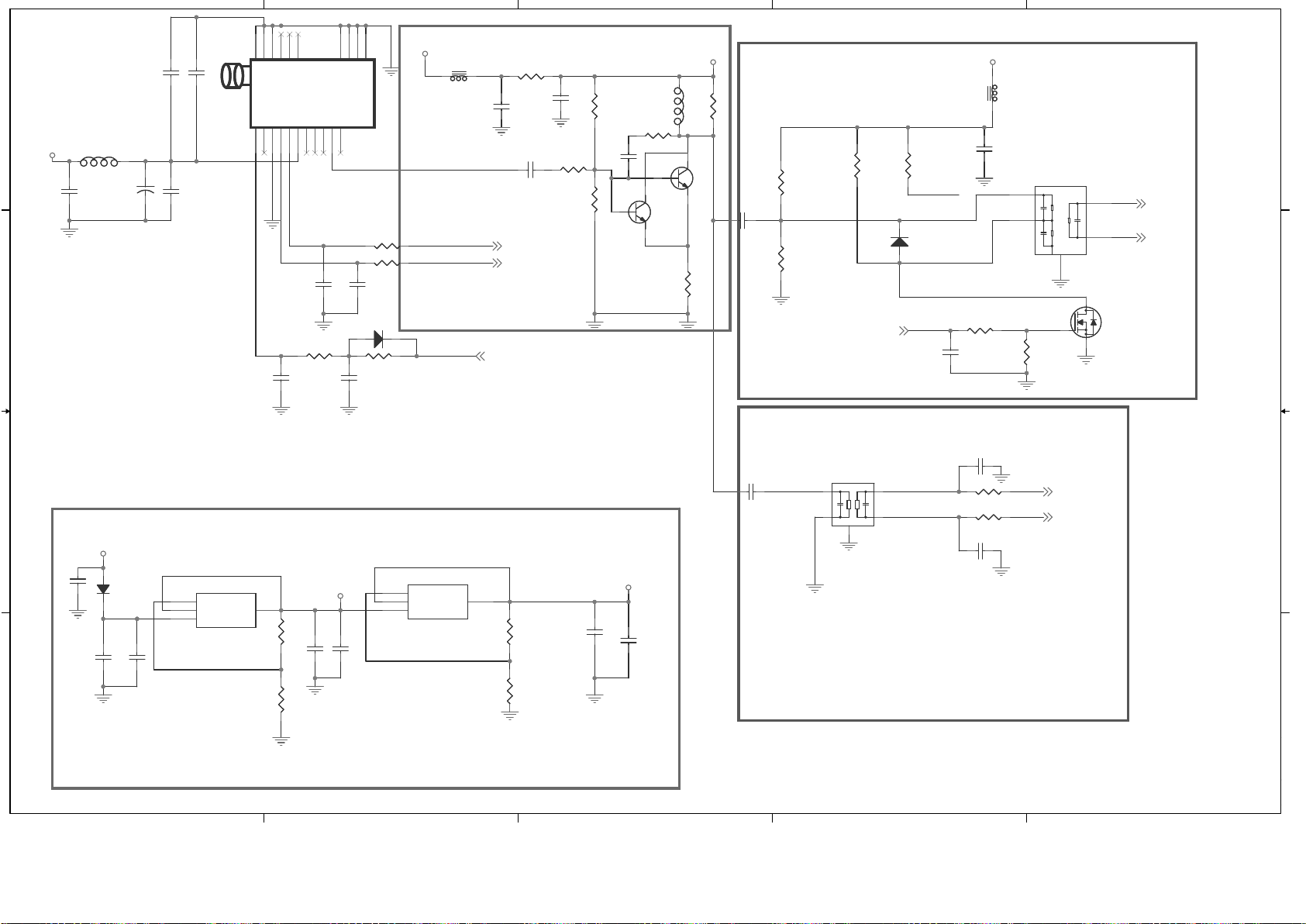
MAIN [3] SCART
Page 37
5
5
4
4
3
3
2
2
1
1
D D
C C
B B
A A
I2C_SDA
SDA
I2C_SCL
SDA
IF_5V
SCL
SCL
TAGCIF-AGC
IF-AGC
SIF_CTL
SIF_CTL
IF_TVP
IF_5V
SIFM
SIFP
VIFP
VIFM
+5V_IF
+8V
+5V_IF
+12V
+5V_IF_1
IF_5V
IF_5V
RF_AGC 7
I2C_SDA
7,12
I2C_SCL 7,12
SIF_VIF_CTRL7
SIFM 7
SIFP 7
VIFP 7
VIFM 7
SIF
Close to IC
Close to IC
Close to Tuner
Tuner VCC
VIF
1 2
R1319
20OHM
R1319
20OHM
12
C1322
0.1UF/16V
C1322
0.1UF/16V
12
C1316
10NF/50V
C1316
10NF/50V
R1331 0OhmR1331 0Ohm
R1306
22KOHM
R1306
22KOHM
D2423
S1D_13_F
D2423
S1D_13_F
12
C131810UF/16V C131810UF/16V
1 2
R1321
220KOHM
R1321
220KOHM
R1323 100OhmR1323 100Ohm
12
C131110UF/10V C131110UF/10V
21
L1301
10UH
L1301
10UH
12
C1310
47PF/50V
C1310
47PF/50V
12
C1323
0.1UF/16V
C1323
0.1UF/16V
R1324 12KOhmR1324 12KOhm
1 2
D1301
1N4148W
D1301
1N4148W
B
C
E
1
2
3
Q1302
BFR520T
B
C
E
1
2
3
Q1302
BFR520T
1 2
R1348
365Ohm
R1348
365Ohm
12
C1312
10NF/50V
C1312
10NF/50V
1 2
C1315 10PF/50V NCC1315 10PF/50V NC
R1317
6.8KOhm
R1317
6.8KOhm
R1332
33Ohm
R1332
33Ohm
12
C251310UF/10VNCC251310UF/10V
NC
1
32
G
S
D
3
2
1
Q1303
2N7002
G
S
D
3
2
1
Q1303
2N7002
12
C1314
0.1UF/16V
C1314
0.1UF/16V
1 2
C1303
10NF/50V
C1303
10NF/50V
12
C1306
0.1UF/16V
C1306
0.1UF/16V
B
C
E
1
2
3
Q2407
BFR92A
NC
B
C
E
1
2
3
Q2407
BFR92A
NC
R1309
6.8KOhm
R1309
6.8KOhm
12
C132610UF/16V C132610UF/16V
1 2
R1347
121Ohm
R1347
121Ohm
12
C1302
10NF/50V
C1302
10NF/50V
1 2
R1305
680OHM
R1305
680OHM
AGC
5
NC1
2
AS
11
SCL12SDA13Vp7Vt8NC21NC34NC410IFout
16
P_GND421P_GND3
20
GND13GND26GND3
9
NC514NC615NC7
17
P_GND118P_GND2
19
TU1301
TT212X
TU1301
TT212X
12
C132010UF/10V C132010UF/10V
12
C1319
0.1UF/16V
C1319
0.1UF/16V
ADJ/GND
1
OUT
2
IN
3
Vout
4
U1303
AP1117EG-13
U1303
AP1117EG-13
1 2
R1304
270Ohm
R1304
270Ohm
R1329 0OhmR1329 0Ohm
R1308
0Ohm
R1308
0Ohm
1 2
R1339
820Ohm
R1339
820Ohm
21
L1302
0.82UH
L1302
0.82UH
R1316 10OHMR1316 10OHM
12
C1321
0.1UF/16V
C1321
0.1UF/16V
12
+
C1324
220UF/16V
+
C1324
220UF/16V
1 2
R1312
2KOHM
R1312
2KOHM
12
C130510UF/10VNCC130510UF/10V
NC
1 2
R1307
680OHM
R1307
680OHM
12
C130710UF/10V C130710UF/10V
2 1
FB1303
120Ohm/100MHz
FB1303
120Ohm/100MHz
1 2
R1322
220KOHM
NC
R1322
220KOHM
NC
1 2
C1317 10PF/50V NCC1317 10PF/50V NC
R1315 10OHMR1315 10OHM
1
2
3
4
5
L1306
36.4MHZ
L1306
36.4MHZ
R1303
6.8KOhm
R1303
6.8KOhm
ADJ/GND
1
OUT
2
IN
3
Vout
4
U1302
AP1117EG-13
U1302
AP1117EG-13
1
2
4
5
3
GND
L1303
36.4MHZ
GND
L1303
36.4MHZ
21
FB1302
120Ohm/100MHz
FB1302
120Ohm/100MHz
12
C1328
0.1UF/16V
C1328
0.1UF/16V
12
C1308
10NF/50V
C1308
10NF/50V
12
C1313
0.1UF/16V
C1313
0.1UF/16V
12
C1309
47PF/50V
C1309
47PF/50V
12
C1304
10NF/50V
C1304
10NF/50V
1 2
R1335
150Ohm
R1335
150Ohm
2 1
D1302
BA591
D1302
BA591
MAIN [4] Tuner I/F
Page 38
5
5
4
4
3
3
2
2
1
1
D D
C C
B B
A A
CEC_E
CEC_E
HPD_B1
HPD_C1
CEC_E
HPD_A1
SCL_A
D2+1
D2-1
D1+1
D1-1
D0-1
CLK-1
CLK+1
D0+1
D2+2
D2-2
D1+2
D1-2
D0+2
D0-2
CLK+2
CLK-2
SDA_B
SCL_A
SDA_A
HDMI_WP
SCL_B
SDA_B
HDMI_WP
SDA_C
HDMI_WP
SDA_A
HPD_A1
SCL_B
SDA_C
SDA_A
SCL_A SCL_B
HPD_B1
SDA_B
SCL_C
HPD_C1
SDA_C
+5V_C
+5V_B
+5V_A
SCL_C
CEC_E
HDMI_WP
HPD_C1
HPD_C
HPD_B1
HPD_B
HPD_A1
HPD_A
CLK-3
D1-3
D0+3
D2+3
D0-3
D2-3
CLK+3
D1+3
SDA_A
SCL_A
SCL_B
SDA_B
SCL_C
SDA_C
HPD_B
HPD_A
HPD_C
SCL_E
SDA_E
OC_S1
OC_S0
OC_S2
OC_S3
EQ_S0
EQ_S1
OC_S0 OC_S1 OC_S2 OC_S3 EQ_S0 EQ_S1
SCL_C
CLK-2
CLK+2
D0-2
D0+2
D1-2
D1+2
D2-2
D2+2
CLK-3
CLK+3
D0-3
D0+3
D1-3
D1+3
D2-3
D2+3
SDA_A
HDMI_WP
+5V_SW +5V_A
+5V_SW +5V_B +5V_SW +5V_C
+5V_C
+5V_B
+5V_A
+3V3_HDMI
+3V3
+5V_SW
+3V3_HD_SW
+3V3_HD_SW
+3V3_STBY
+3V3_STBY
+3V3
+5V_SW
+3V3_HDMI
DDC_WP 7
DDC_DSUB_WP1
R_1TX2+ 7
R_1TX2- 7
TXCLK1- 7
TXCLK1+ 7
B_1TX0- 7
B_1TX0+ 7
G_1TX1- 7
G_1TX1+ 7
SDA_HD1 7
SCL_HD1 7
HPD 7
CEC_HDMI 7
HDMI_S3
HDMI_S1
HDMI_S2
Side HDMI
OC_S2
OC_S1 OC_S0
OC_S3
Vswing (mV)
Pre/De
emphasis (dB)
0
0
0
0
0
0
0
0
0
0
0
0
0
0
0
0
0
0
0
0
0
0
0
0
0
0
0
0
0
0
0
0
333
500
666
1000
160
270
340
500
500
500
500
500
600
1000
750
500
-9.5
-6
-3.5
0
-9
-6
-3.5
0
6
3.5
1.5
0
0
0
0
0
1
1
1
1
1
1
1
1
1
1
1
1
1
1
1
1
1
1
1
1
1
1
1
1
1
1
1
1
1
1
1
1
EQ_S1
15dB on all high speed data inputs
3dB on all high speed data inputs
8dB on all high speed data inputs
EQ_S0
000
01
1
1
1 Optimized Equalization on all high
speed data input (Default setting
from 1m to 20m)
S1 S2 S3
L
L
Port 1
Port 2
Port 3LLL L
H
H
H
X X
X
/OE
Close to Connector
Close to Connector
Close to Connector
Close to connector
12
ZD1403
ADUC10S03005
NC
ZD1403
ADUC10S03005
NC
1
4
2
3
L1401
90Ohm/100MHz
NC
L1401
90Ohm/100MHz
NC
1 2
C1416
0.1UF/16V
C1416
0.1UF/16V
B
C
E
1
2
3
Q1406
PMBS3904
B
C
E
1
2
3
Q1406
PMBS3904
1
4
2
3
L1412
90Ohm/100MHz
NC
L1412
90Ohm/100MHz
NC
1 2
C1418
0.1UF/16V
C1418
0.1UF/16V
12
R2351
0Ohm
NC
R2351
0Ohm
NC
12
C1444 22PF/50VC1444 22PF/50V12C1443 22PF/50VC1443 22PF/50V
R1412 0OhmR1412 0Ohm
R1426 1KOhmR1426 1KOhm
12
C14100.1UF/16VNCC14100.1UF/16V
NC
1 2
R1446 22KOHMR1446 22KOHM
12
R2355
0Ohm
NC
R2355
0Ohm
NC
1 2
ZD1416 ADUC10S03005 NCZD1416 ADUC10S03005 NC
1 2
R1445 22KOHMR1445 22KOHM
1
4
2
3
L1403
90Ohm/100MHz
NC
L1403
90Ohm/100MHz
NC
R1440 4.7KOhmR1440 4.7KOhm
1
2
3
D1402
BAT54C
D1402
BAT54C
1
4
2
3
L1407
90Ohm/100MHz
NC
L1407
90Ohm/100MHz
NC
1 2
C1406
0.1UF/16V
C1406
0.1UF/16V
R1454 4.7KOhmR1454 4.7KOhm
12
C1445 22PF/50VC1445 22PF/50V
R1437 4.7KOhmNCR1437 4.7KOhm
NC
1 2
C1415
0.1UF/16V
C1415
0.1UF/16V
1 2
C1423
0.1UF/16V
C1423
0.1UF/16V
1 2
C1421
0.1UF/16V
C1421
0.1UF/16V
1 2
ZD1414 ADUC10S03005 NCZD1414 ADUC10S03005 NC
1 2
C1409
0.1UF/16V
NC
C1409
0.1UF/16V
NC
1 2
C1419
0.1UF/16V
C1419
0.1UF/16V
1
4
2
3
L1404
90Ohm/100MHz
NC
L1404
90Ohm/100MHz
NC
12
R2349
0Ohm
NC
R2349
0Ohm
NC
B
C
E
1
2
3
Q1407
PMBS3904
B
C
E
1
2
3
Q1407
PMBS3904
SDA11SCL12CLK-13CLK+14VDD15D0-16D0+17D1-18D1+19VDD210D2-111D2+112VDD313OC_S114OC_S015OC_S2
16
S1
17
S2
18
S3
19
D2+
20
D2-
21
VDD4
22
D1+
23
D1-
24
D0+
25
D0-
26
VDD5
27
CLK+
28
CLK-
29
SCL_SINK
30
SDA_SINK
31
HPD_SINK
32
EQ_S0
33
OE#
34
VDD635HPD3
36
SDA3
37
SCL3
38
CLK-3
39
CLK+3
40
VDD7
41
D0-3
42
D0+3
43
D1-3
44
D1+3
45
VDD8
46
D2-3
47
D2+3
48
EQ_S1
49
HPD2
50
SDA2
51
SCL2
52
CLK-2
53
CLK+2
54
VDD9
55
D0-2
56
D0+2
57
D1-2
58
D1+2
59
VDD10
60
D2-2
61
D2+2
62
HPD1
63
OC_S3
64
GND
65
U1401
PI3HDMI301ZLE
U1401
PI3HDMI301ZLE
R1429
0OHM
NC
R1429
0OHM
NC
1 2
R1447 22KOHM
NC
R1447 22KOHM
NC
1 2
C1422
0.1UF/16V
C1422
0.1UF/16V
R1458 4.7KOhm
NC
R1458 4.7KOhm
NC
R1441 4.7KOhmR1441 4.7KOhm
1
4
2
3
L1408
90Ohm/100MHz
NC
L1408
90Ohm/100MHz
NC
12
ZD1407
ADUC10S03005
NC
ZD1407
ADUC10S03005
NC
R1409 4.7KOhm NCR1409 4.7KOhm NC
12
R2346
0Ohm
NC
R2346
0Ohm
NC
R1444 4.7KOhmR1444 4.7KOhm
12
ZD1404
PESD0603-240
NC
ZD1404
PESD0603-240
NC
R1455
4.7KOhm
R1455
4.7KOhm
12
C14271PF/50VNCC14271PF/50V
NC
R1430
200Ohm
R1430
200Ohm
12
ZD1411
PESD0603-240
NCZD1411
PESD0603-240
NC
R1424
47KOHM
R1424
47KOHM
R1427
100Ohm
R1427
100Ohm
12
ZD1406
PESD0603-240
NCZD1406
PESD0603-240
NC
1
1
2
2
3
3
4
4
5
5
6
6
7
7
8
8
9
9
10
10
11
11
12
12
13
13
14
14
15
15
16
16
17
17
18
18
19
19
P_GND1
20
P_GND2
21
P_GND3
22
P_GND4
23
CN1404
HDMI_CON_19P
NC
CN1404
HDMI_CON_19P
NC
B
C
E
1
2
3
Q1408
PMBS3904
NC
B
C
E
1
2
3
Q1408
PMBS3904
NC
R143910KOhm R143910KOhm
1 2
C1417
0.1UF/16V
C1417
0.1UF/16V
R143610KOhmNCR143610KOhm
NC
12
C14251PF/50VNCC14251PF/50V
NC
1
2
3
D1403
BAT54C
D1403
BAT54C
B
C
E12
3
Q1402
BC847C-7-F
B
C
E12
3
Q1402
BC847C-7-F
1
2
3
D1401
BAT54C
NC
D1401
BAT54C
NC
12
C1408
22PF/50V
NC
C1408
22PF/50V
NC
1
4
2
3
L1409
90Ohm/100MHz
NC
L1409
90Ohm/100MHz
NC
R1413 0OhmR1413 0Ohm
1 2
ZD1415 ADUC10S03005 NCZD1415 ADUC10S03005 NC
R1656 10KO hm NCR1656 10KOhm NC
1 2
C1424
0.1UF/16V
C1424
0.1UF/16V
12
C14261PF/50VNCC14261PF/50V
NC
12
ZD1408
PESD0603-240
NCZD1408
PESD0603-240
NC
R1433 1KOhm
NC
R1433 1KOhm
NC
1
2
3
D1405
BAT54C
D1405
BAT54C
12
C1414
10UF/10V
C1414
10UF/10V
21
FB1405 120Ohm/100MhzFB1405 120Ohm/100Mhz
12
R2357
0Ohm
NC
R2357
0Ohm
NC
R1404 4.7KOhmR1404 4.7KOhm
R1456 4.7KOhmR1456 4.7KOhm
E0
1
E1
2
E2
3
Vss
4
Vcc
8
WC#
7
SCL
6
SDA
5
U1404
M24C02_WMN6TP
U1404
M24C02_WMN6TP
21
FB1404
120Ohm/100Mhz
NC
FB1404
120Ohm/100Mhz
NC
E0
1
E1
2
E2
3
Vss
4
Vcc
8
WC#
7
SCL
6
SDA
5
U1402
M24C02_WMN6TP
NC
U1402
M24C02_WMN6TP
NC
12
C1413
0.1UF/16V
C1413
0.1UF/16V
1
4
2
3
L1410
90Ohm/100MHz
NC
L1410
90Ohm/100MHz
NC
21
FB1402
120Ohm/100Mhz
FB1402
120Ohm/100Mhz
1 2
C1405
0.1UF/16V
C1405
0.1UF/16V
12
C14110.1UF/16V C14110.1UF/16V
1
4
2
3
L1405
90Ohm/100MHz
NC
L1405
90Ohm/100MHz
NC
E0
1
E1
2
E2
3
Vss
4
Vcc
8
WC#
7
SCL
6
SDA
5
U1403
M24C02_WMN6TP
U1403
M24C02_WMN6TP
1 2
R1453 1.5KOHM
NC
R1453 1.5KOHM
NC
12
ZD1410
PESD0603-240
NCZD1410
PESD0603-240
NC
1 2
R1448 1.5KOHMR1448 1.5KOHM
1
32
G
S
D
3
2
1
Q1401
SI2302ADS
G
S
D
3
2
1
Q1401
SI2302ADS
12
C14280.1UF/16V C14280.1UF/16V
12
ZD1412
PESD0603-240
NC
ZD1412
PESD0603-240
NC
21
FB1403
120Ohm/100Mhz
FB1403
120Ohm/100Mhz
1 2
C1420
0.1UF/16V
C1420
0.1UF/16V
R1438 4.7KOhmNCR1438 4.7KOhm
NC
1
4
2
3
L1411
90Ohm/100MHz
NC
L1411
90Ohm/100MHz
NC
R142810KOhm R142810KOhm
12
ZD1402
ADUC10S03005
NC
ZD1402
ADUC10S03005
NC
R1716
10KOhm
R1716
10KOhm
1 2
R1452 1.5KOHMR1452 1.5KOHM
12
ZD1405
PESD0603-240
NCZD1405
PESD0603-240
NC
12
R2353
0Ohm
NC
R2353
0Ohm
NC
12
C14120.1UF/16V C14120.1UF/16V
R1421 1KOhmR1421 1KOhm
1
4
2
3
L1402
90Ohm/100MHz
NC
L1402
90Ohm/100MHz
NC
R1459
4.7KOhm
NC
R1459
4.7KOhm
NC
1
1
2
2
3
3
4
4
5
5
6
6
7
7
8
8
9
9
10
10
11
11
12
12
13
13
14
14
15
15
16
16
17
17
18
18
19
19
P_GND2
21
P_GND3
22
P_GND4
23
P_GND5
24
P_GND1
20
CN1402
HDMI_CON_19P
CN1402
HDMI_CON_19P
1
4
2
3
L1406
90Ohm/100MHz
NC
L1406
90Ohm/100MHz
NC
R1405 4.7KOhmR1405 4.7KOhm
R1457
4.7KOhm
R1457
4.7KOhm
R144210KOhm R144210KOhm
R1443 4.7KOhmR1443 4.7KOhm
R1425
47KOHM
NC
R1425
47KOHM
NC
1
1
2
2
3
3
4
4
5
5
6
6
7
7
8
8
9
9
10
10
11
11
12
12
13
13
14
14
15
15
16
16
17
17
18
18
19
19
P_GND2
21
P_GND3
22
P_GND4
23
P_GND5
24
P_GND1
20
CN1403
HDMI_CON_19P
CN1403
HDMI_CON_19P
MAIN [5] HDMI
Page 39
5
5
4
4
3
3
2
2
1
1
D D
C C
B B
A A
MVREF-D
MDATA[0..15]
DATA0
DATA1
DATA2
DATA3 MDATA3
MDATA1
MDATA2
MDATA0
DATA7
DATA4
DATA5
DATA6
MDATA7
MDATA4
MDATA5
MDATA6
DATA8
DATA9
DATA10
DATA11
MDATA9
MDATA10
MDATA8
MDATA11
DATA12
DATA13
DATA14
DATA15
MDATA14
MDATA13
MDATA12
MDATA15
DATA4
DATA5
DATA7
DATA6
DATA0
DATA1
DATA2
DATA3
DATA8
DATA9
DATA10
DATA11
DATA12
DATA13
DATA14
DATA15
256M
MADR11
MADR7
MADR1
MADR10
MADR5
MADR6
MADR3
MADR0
MADR4
MADR8
MADR2
MADR9
MADR[0..11]MADR[0..11]
ADR11
ADR7
ADR1
ADR10
ADR5
ADR6
ADR3
ADR0
ADR4
ADR8
ADR2
ADR9
MCLK+
MCLK-
CKE
RASZMRASZ
CASZ CASZM
WEZMWEZ
UDQS
LDQS
DQS1
DQS0
LDQM
UDQM DQMS1
DQMS0
BA1
BA0
MVREF-D
SPI_FDO
MCLK+
MCLK-
DMC
DMC
+2V6
DMC
DMC
+3V3_STBY
DMC
MDATA[0..15] 7
MADR[0..11]7
CKE7
RASZ7
CASZ7
WEZ7
DQS07
DQS17
UDQM7
LDQM7
BA07
BA17
SPI_CK 7
SPI_DI 7
SPI_WP7
SPI_CZ7
SPI_DO7
MCLK7
MCLKZ7
12
C1807
0.1UF/16V
C1807
0.1UF/16V
12
C1813
0.1UF/16V
C1813
0.1UF/16V
21
FB1801 120Ohm/100MhzFB1801 120Ohm/100Mhz
R1803 100OhmR1803 100Ohm
R1804 100OhmR1804 100Ohm
R1810 47OhmR1810 47Ohm
R1812 56OhmR1812 56Ohm
R1806 100OhmR1806 100Ohm
1 2
RN1805A
56Ohm
RN1805A
56Ohm
5 6
RN1802C
56Ohm
RN1802C
56Ohm
12
C1814
0.1UF/16V
C1814
0.1UF/16V
5 6
RN1805C
56Ohm
RN1805C
56Ohm
3 4
RN1802B
56Ohm
RN1802B
56Ohm
R1807 100OhmR1807 100Ohm
1 2
RN1806A
56Ohm
RN1806A
56Ohm
R1814 56OhmR1814 56Ohm
R1809 47OhmR1809 47Ohm
12
C1819
4.7PF/50V
NC
C1819
4.7PF/50V
NC
R1817 22OhmR1817 22Ohm
12
C1805
10NF/50V
C1805
10NF/50V
12
C1820
4.7PF/50V
NC
C1820
4.7PF/50V
NC
5 6
RN1801C
56Ohm
RN1801C
56Ohm
3 4
RN1806B
56Ohm
RN1806B
56Ohm
1 2
R1808
10KOHM
R1808
10KOHM
1 2
RN1807A
56Ohm
RN1807A
56Ohm
1 2
RN1801A
56Ohm
RN1801A
56Ohm
1 2
R1801
10KOHM
R1801
10KOHM
7 8
RN1803D
56Ohm
RN1803D
56Ohm
12
C1801
10UF/10V
C1801
10UF/10V
12
C1816
0.1UF/16V
C1816
0.1UF/16V
12
C1806
10NF/50V
C1806
10NF/50V
12
C1803
4.7UF/10V
C1803
4.7UF/10V
12
C1809
0.1UF/16V
C1809
0.1UF/16V
3 4
RN1804B
56Ohm
RN1804B
56Ohm
R1805 0Ohm
NC
R1805 0Ohm
NC
3 4
RN1803B
56Ohm
RN1803B
56Ohm
5 6
RN1807C
56Ohm
RN1807C
56Ohm
12
C1817
1000PF/50V
C1817
1000PF/50V
12
C1802
0.1UF/16V
C1802
0.1UF/16V
7 8
RN1805D
56Ohm
RN1805D
56Ohm
12
C1811
0.1UF/16V
C1811
0.1UF/16V
12
C1808
0.1UF/16V
C1808
0.1UF/16V
R1802
10KOhm
R1802
10KOhm
R1815150Ohm R1815150Ohm
1 2
RN1803A
56Ohm
RN1803A
56Ohm
12
C1810
0.1UF/16V
C1810
0.1UF/16V
3 4
RN1805B
56Ohm
RN1805B
56Ohm
R1813 56OhmR1813 56Ohm
7 8
RN1802D
56Ohm
RN1802D
56Ohm
7 8
RN1806D
56Ohm
RN1806D
56Ohm
12
C1804
4.7UF/10V
C1804
4.7UF/10V
5 6
RN1806C
56Ohm
RN1806C
56Ohm
1 2
RN1802A
56Ohm
RN1802A
56Ohm
R1816 56OhmR1816 56Ohm
7 8
RN1807D
56Ohm
RN1807D
56Ohm
A0
29
A1
30
A10/AP
28
A11
41
A2
31
A3
32
A4
35
A5
36
A6
37
A7
38
A8
39
A9
40
BA0
26
BA1
27
CAS#
22
CKE
44
CLK
45
CLK#
46
CS#
24
DQ0
2
DQ1
4
DQ10
57
DQ11
59
DQ12
60
DQ13
62
DQ14
63
DQ15
65
DQ2
5
DQ3
7
DQ4
8
DQ5
10
DQ6
11
DQ7
13
DQ8
54
DQ9
56
LDM
20
LDQS
16
NC1
14
NC2
17
NC3
19
NC4
25
NC5
42
NC6
43
NC7
50
NC8
53
RAS#
23
UDM
47
UDQS
51
VDD1
1
VDD2
18
VDD3
33
VDDQ1
3
VDDQ2
9
VDDQ3
15
VDDQ4
55
VDDQ5
61
VREF
49
VSS1
34
VSS2
48
VSS3
66
VSSQ1
6
VSSQ2
12
VSSQ3
52
VSSQ4
58
VSSQ5
64
WE#
21
U1802
W9412G6IH-4
U1802
W9412G6IH-4
7 8
RN1801D
56Ohm
RN1801D
56Ohm
CS#
1
SO/SIO1
2
WP#/ACC
3
SI/SIO0
5
SCLK
6
HOLD#
7
VCC
8
GND
4
U1801
MX25L1605DM2I-12G
U1801
MX25L1605DM2I-12G
3 4
RN1801B
56Ohm
RN1801B
56Ohm
3 4
RN1807B
56Ohm
RN1807B
56Ohm
5 6
RN1803C
56Ohm
RN1803C
56Ohm
1 2
RN1804A
56Ohm
RN1804A
56Ohm
12
C1815
0.1UF/16V
C1815
0.1UF/16V
7 8
RN1804D
56Ohm
RN1804D
56Ohm
12
C1812
0.1UF/16V
C1812
0.1UF/16V
5 6
RN1804C
56Ohm
RN1804C
56Ohm
12
C1821
4.7PF/50V
NC
C1821
4.7PF/50V
NC
R1811 47OhmR1811 47Ohm
21
FB1802 120Ohm/100MhzFB1802 120Ohm/100Mhz
MAIN [8] Flash/DDR
Page 40

5
5
4
4
3
3
2
2
1
1
D D
C C
B B
A A
MVREF
I2C_SDA
I2C_SCL
I2C_SCL
I2C_SDA
TXD
RXD
MDATA9
MADR6
MDATA0
MDATA12
XOUT
MADR9
MADR7
MDATA1
LDQM
DQS0
XIN
MDATA10
NVRAM_WP
CKE
MDATA14
RASZ
BA0
BA1
MDATA4
MDATA13
MADR10
MDATA5
MADR1
DQS1
UDQM
MADR0
WEZ
MDATA6
MADR8
MDATA2
MDATA8
MADR5
MDATA3
MVREF
MDATA11
MDATA15
MADR11
MADR3
CASZ
MDATA7
MADR4
MADR2
NVRAM_WP
PWM2
MCLKZ
MCLK
PWM0
AVDD_MPLL
VDDP
AVDDA
+1V2 VDDC
+2V6
AVDD_MemPLL+3V3
AVDD_USB2+3V3
AVDD_AU+3V3
VDDM
VDDM
AVDD_VIF1+3V3
AVDD_VIF2+3V3
AVDD_VIF5+3V3
+3V3_STBY
VDDM
AVDDA
AVDD_VIF2
AVDD_AU
AVDD_VIF5
AVDD_MemPLL
AVDD_MPLL
AVDD_VIF1
AVDD_USB2
VDDC VDD_PM VDDP
AVDDA
+3V3_STBY
+3V3_STBY
+3V3_STBY
VDD_PM
+3V3_STBY
+3V3_STBY
+3V3_STBY
+3V3_STBY
+3V3_STBY
IF_5V
+3V3_STBY
+3V3_STBY
SIF_VIF_CTRL 4
HP_DET 12
USB_PWR_SW 11
AUDIO_MUX 2
USB_OC_DET 11
HP_MUTE 12
BA1 8
CASZ 8
WEZ 8
RASZ 8
BA0 8
MDATA[0..15] 8
MADR[0..11] 8
LDQM 8
DQS0 8
UDQM 8
DQS1 8
MCLKZ 8
MCLK 8
CKE 8
RXO0- 10
RXO1- 10
RXE0+ 10
RXE1- 10
RXO3+ 10
RXE0- 10
RXO2+ 10
RXE3+ 10
RXE2+ 10
RXOC+ 10
RXO3- 10
RXEC+ 10
RXO2- 10
RXE3- 10
RXE2- 10
RXOC- 10
RXO0+ 10
RXEC- 10
RXO1+ 10
RXE1+ 10
HDMI_S3 10
USB2_DM 11
USB2_DP 11
ACDetect 6,12
G_1TX1-5
TXCLK1+5
B_1TX0+5
R_1TX2+5
TXCLK1-5
R_1TX2-5
B_1TX0-5
G_1TX1+5
SCL_HD15
SDA_HD15
HS_RGB1
GIN+1
SOG1
BIN+1
VS_RGB1
RIN+1
SCART_G3
SCART_B3
SCART_R3
Y2+2
SOY22
PB2+2
PR2+2
AV_CVBS2
AV_VCOM2
CVBSOUT3
AUL13
AUR03
AUL03
AUR13
AUR32
AUL32
AUR22
AUL22
LineoutR3
LineoutL3
SIFM4
SIFP4
VIFP4
VIFM4
ISP2_SCL1
I2C_SDA4,12
I2C_SCL4,12
ISP2_SDA1
SPI_CZ8
SPI_CK8
SPI_DI8
SPI_DO8
KEY29
RC_IR9
BL_ADJ6
SPI_WP8
CEC_HDMI 5
RF_AGC4
LINEOUT_MUTE3
BL_EN6
5V_PWR_SW13
STANDBY6
PANEL_PWR13
LED_ON_OFF9
LED_TIMER9
DDC_WP5
KEY19
AUOutL12
AUOutR12
RXO4+ 10
RXO4- 10
RXE4+ 10
RXE4- 10
SC1_AV_Out3
SC2_FS3
SCC3
SCY3
SC1_FS3
SC1_FSW3
AMP_RESET 12
AMP_MUTE 12
AU2MCKO12
AU2WS12
AU2SCK12
AU2SDO12
SC1_AV3
HDMI_S1 5
HDMI_S2 5
HPD5
Panel_S1
Panel_S2
OD_SEL 5
3V3_AMP_SW
SC1_SOG
+2.6V for VDDM
Pin111, Pin127, Pin132, Pin138, Pin143,Pin149,Pin154
Pin61
+3.3V for AVDD_VIF5
Pin52
+3.3V for AVDD_VIF2
Pin59
+3.3V for AVDD_VIF1
+3.3V for AVDD_MemPLL
Pin124
+3.3V for AVDD_AU
Pin64, Pin69
Pin162
+3.3V for AVDD_USB2
+1.2V for VDDC
Pin98, Pin109, Pin173, Pin209, Pin242
Pin96, Pin166, Pin186, Pin195, Pin202, Pin222, Pin236
+3.3V_STBY for VDDP
Pin48
+3.3V_STBY for AVDD_MPLL
Pin18, Pin37, Pin245
+3.3V_STBY for AVDDA
I2C address at A0
NVRAM
Close to IC
Change from 47K to 4.7K by Jason
CVBSOUT / SCART2
SCART 1/2
SCART_SV
SCART1
12
C1668
0.1UF/16V
C1668
0.1UF/16V
12
C1610
0.1UF/16V
C1610
0.1UF/16V
R1704 33KOhmR1704 33KOhm
2
1
HEATSINK1
HEATSINK
NC
HEATSINK1
HEATSINK
NC
1 2
C1629 0.1UF/16VC1629 0.1UF/16V
12
C1630 0.047UF/10VC1630 0.047UF/10V
R1603
10KOhm
R1603
10KOhm
1 2
C1628 0.1UF/16VC1628 0.1UF/16V
21
FB1604 120Ohm/100MHzFB1604 120Ohm/100MHz
R1707 100OhmR1707 100Ohm
1 2
C1652
0.1UF/16V
C1652
0.1UF/16V
12
C1633
0.1UF/16V
C1633
0.1UF/16V
12
C1664
10UF/10V
C1664
10UF/10V
R1623 10OHMR1623 10OHM
R1617 10OHMR1617 10OHM
12
C1653
10UF/10V
C1653
10UF/10V
R1668 10KOhm NCR1668 10KOhm NC
21
FB1601 120Ohm/100MhzFB1601 120Ohm/100Mhz
12
C1639
10UF/10V
C1639
10UF/10V
R1607 100OhmR1607 100Ohm
12
C1623
0.1UF/16V
C1623
0.1UF/16V
12
C1613
0.1UF/16V
C1613
0.1UF/16V
21
FB1611 120Ohm/100MhzFB1611 120Ohm/100Mhz
R1679 47OhmR1679 47Ohm
12
C1621
22UF/6.3V
C1621
22UF/6.3V
R1616 10OHMR1616 10OHM
R1678 47OhmR1678 47Ohm
R1667 10KOhm NCR1667 10KOhm NC
12
C1677
100PF/50V
C1677
100PF/50V
R1611 10OHMR1611 10OHM
R1647 47OhmR1647 47Ohm
R1684 1KOhmR1684 1KOhm
12
C1663
0.1UF/16V
C1663
0.1UF/16V
R1703
100Ohm
R1703
100Ohm
R1708 100OhmR1708 100Ohm
12
C1669
0.1UF/16V
C1669
0.1UF/16V
R1680 47OhmR1680 47Ohm
12
C1604
0.1UF/16V
C1604
0.1UF/16V
R1686 100OhmR1686 100Ohm
1 2
R1719
10KOHM
R1719
10KOHM
12
C1649
0.1UF/16V
C1649
0.1UF/16V
1 2
C1645
2.2UF/16V
C1645
2.2UF/16V
12
C170210PF/50VNC C170210PF/50VNC
1 2
R1605
1MOhm
R1605
1MOhm
R1626 47OhmR1626 47Ohm
R1730
47KOHM
R1730
47KOHM
12
C1644 0.1UF/16VC1644 0.1UF/16V
12
C1660
100PF/50V
C1660
100PF/50V
12
C1607
15PF/50V
C1607
15PF/50V
12
C1624
0.1UF/16V
C1624
0.1UF/16V
21
FB1610 120Ohm/100MhzFB1610 120Ohm/100Mhz
R1633 56OhmR1633 56Ohm
R1702 33KOhmR1702 33KOhm
R1700 33KOhmR1700 33KOhm
1 2
C1619 0.1UF/16VC1619 0.1UF/16V
R1645 47OhmR1645 47Ohm
12
C1675 47NF/25VC1675 47NF/25V
12
C1611
10UF/10V
C1611
10UF/10V
R1622
390Ohm
R1622
390Ohm
12
C1666
0.1UF/16V
C1666
0.1UF/16V
1 2
GND
3
X1601
14.318Mhz
1 2
GND
3
X1601
14.318Mhz
R1655 47OhmR1655 47Ohm
12
C1646
10UF/10V
C1646
10UF/10V
R1606 100OhmR1606 100Ohm
R1670 47OhmR1670 47Ohm
R1674 47OhmR1674 47Ohm
R1614 10OHMR1614 10OHM
12
C1635
0.1UF/16V
C1635
0.1UF/16V
R1672 47OhmR1672 47Ohm
R1650 22OhmR1650 22Ohm
1 2
C1638
1UF/16V
C1638
1UF/16V
GND
1
RESET
2
VCC
3
U1601
G690H293T73UF
U1601
G690H293T73UF
R1673 47OhmR1673 47Ohm
12
C1626
0.1UF/16V
C1626
0.1UF/16V
R1706 100OhmR1706 100Ohm
R1638
0Ohm
R1638
0Ohm
21
FB1613 120Ohm/100MhzFB1613 120Ohm/100Mhz
R1644 47OhmR1644 47Ohm
12
C1605
0.1UF/16V
C1605
0.1UF/16V
R1683 47OhmR1683 47Ohm
R1613 10OHMR1613 10OHM
12
C1606
0.1UF/16V
C1606
0.1UF/16V
R1621 10OHMR1621 10OHM
R1695 3.3KOHMR1695 3.3KOHM
R1722 100OhmR1722 100Ohm
R1624 47OhmR1624 47Ohm
R1602
470Ohm
R1602
470Ohm
1 2
C1640
0.1UF/16V
C1640
0.1UF/16V
R1612 10OHMR1612 10OHM
R1705 33KOhmR1705 33KOhm
R1609 100OhmR1609 100Ohm
1 2
R1639
5.6KOHM
R1639
5.6KOHM
12
C1674
1000PF/50V
C1674
1000PF/50V
R1627
100Ohm
NCR1627
100Ohm
NC
R1625 47OhmR1625 47Ohm
12
C1676
10UF/10V
NC
C1676
10UF/10V
NC
R1620
430OHM
R1620
430OHM
12
C1614
0.1UF/16V
C1614
0.1UF/16V
21
FB1607 120Ohm/100MhzFB1607 120Ohm/100Mhz
12
C1617
0.1UF/16V
C1617
0.1UF/16V
R1636
4.7KOhm
R1636
4.7KOhm
R1654 22OhmR1654 22Ohm
12
C1641
10UF/10V
C1641
10UF/10V
R1696 3.3KOHMR1696 3.3KOHM
R1682 47OhmR1682 47Ohm
R1681 47OhmR1681 47Ohm
R1652 22OhmR1652 22Ohm
1 2
D1601
1N4148W
NC
D1601
1N4148W
NC
R1648 22OhmR1648 22Ohm
12
C1643
0.1UF/16V
C1643
0.1UF/16V
12
C1627 0.047UF/10VC1627 0.047UF/10V
R1697 33KOhmR1697 33KOhm
R1671 100OhmR1671 100Ohm
12
C1659
0.1UF/16V
C1659
0.1UF/16V
12
C170110PF/50VNC C170110PF/50VNC
12
C1634
10UF/10V
C1634
10UF/10V
12
C1661
100PF/50V
C1661
100PF/50V
R1642 4 7OhmR1642 47 Ohm
12
C1608
15PF/50V
C1608
15PF/50V
12
C1625
0.1UF/16V
C1625
0.1UF/16V
R1619
470Ohm
R1619
470Ohm
R1635
4.7KOhm
R1635
4.7KOhm
R1685 47OhmR1685 47Ohm
12
C1658
10UF/10V
C1658
10UF/10V
R1712
4.7KOhm
R1712
4.7KOhm
R1649 47OhmR1649 47Ohm
1 2
C1650
0.1UF/16V
C1650
0.1UF/16V
R1634 56OhmR1634 56Ohm
R1688 100OhmR1688 100Ohm
12
C1618
0.1UF/16V
C1618
0.1UF/16V
21
FB1608 120Ohm/100MhzFB1608 120Ohm/100Mhz
R1687 1KOhmR1687 1KOhm
12
C1615
0.1UF/16V
C1615
0.1UF/16V
12
C1665
0.1UF/16V
C1665
0.1UF/16V
21
FB1603 120Ohm/100MhzFB1603 120Ohm/100Mhz
1 2
R1717
10KOHM
R1717
10KOHM
R1608 47OhmR1608 47Ohm
21
FB1606 120Ohm/100MhzFB1606 120Ohm/100Mhz
R1604 100OhmR1604 100Ohm
12
C1662
10UF/10V
C1662
10UF/10V
12
C1671
0.1UF/16V
C1671
0.1UF/16V
12
C1632
0.1UF/16V
C1632
0.1UF/16V
R1637
4.7KOhm
R1637
4.7KOhm
12
C1637
4.7UF/10V
C1637
4.7UF/10V
12
C1647
0.1UF/16V
C1647
0.1UF/16V
12
C1601
10UF/10V
C1601
10UF/10V
12
C1648
100PF/50V
C1648
100PF/50V
12
C1609
10UF/10V
C1609
10UF/10V
GND1
1
RXCKP
244
GND3
40
RXCKN
243
TAGC
63
RX0N
246
RX0P
247
AVDD_33_4
245
RX1N
249
RX1P
250
GND_VIFPLL
49
HPLUG
254
REXT
2
DDCD_SDA
255
DDCD_SCL
256
HSYNC1
3
VSYNC1
4
VCLAMP
5
REFP
6
REFM
7
BIN1P
8
SOGIN1
9
GIN1P
10
RIN1P
11
VCOM2
12
BIN0P
13
VCOM3
14
RIN0P
17
AVDD_33_2
37
GND_RXS
53
HSYNC0
20
VSYNC0
21
VSYNC2
22
BIN2P
23
SOGIN2
24
GIN2P
25
RIN2P
26
C1
27
Y1
28
C0
29
Y0
30
CVBS3
31
CVBS2
32
CVBS1
33
VCOM1
34
CVBS0
35
VCOM0
36
AVDD_33_1
18
CVBSOUT1
38
GPIOD[0]
88
GPIOD[1]
89
GPIOD[2]
90
GPIOD[3]
91
GPIOD[4]
92
GPIOD[5]
93
GPIOD[6]
94
GPIOD[7]
95
VR27
50
GND4
65
DQS1
155
MDATA[15]
153
MDATA[14]
152
GND5
97
MDATA[12]
150
AVDD_MI5
143
MDATA[11]
148
MDATA[10]
147
BADR[1]
106
GND7
126
AVDD_MI4
138
MDATA[7]
142
MDATA[6]
141
MDATA[4]
139
AVDD_MI3
132
MDATA[3]
137
MDATA[2]
136
MDATA[1]
134
MDATA[0]
133
DQS0
131
DQM0
130
MVREF
160
MCLKE
159
MCLKZ
157
MCLK
158
TAFC
60
GND9
146
AVDD_MI2
127
AVDD_MIPLL
128
CASZ
112
WEZ
113
MADR[0]
125
MADR[1]
124
MADR[2]
123
MADR[3]
122
MADR[4]
121
AVDD_MI1
111
VDDC4
209
MADR[8]
117
VDDP6
222
SPI_SCK
168
ALE
105
GND13
208
SPI_SDI
169
SPI_SCZ
170
SPI_SDO
171
SAR1
175
SAR2
176
SAR3
177
PWM0
178
PWM1
179
DDCR_SDA
180
DDCA_SDA
182
MADR[6]
119
VDDP7
236
VDDP5
202
GND14
223
VDDC3
173
NC5
188
NC6
189
PWM3
194
VDDC2
109
VDDP4
195
LVA3P
212
LVA3M
213
LVACKP
214
LVACKM
215
LVA2P
216
LVA2M
217
LVA1P
218
LVA1M
219
LVA0P
220
LVA0M
221
VDDP3
186
INT
184
LVB3P
226
LVB3M
227
LVBCKP
228
LVBCKM
229
LVB2P
230
LVB2M
231
LVB1P
232
LVB1M
233
LVB0P
234
LVB0M
235
VDDP2
166
RDZ
104
VDDP1
96
DI[4]
203
DI[6]
205
DI[7]
206
VDDC1
98
HWRESET
207
XOUT
46
XIN
47
AVDD_MPLL
48
VR12
51
VIFP
57
RX2P
253
RX2N
252
PWM2
193
GPIOE[1]
240
GPIOE[0]
241
GIN0P
15
SOGIN0
16
CVBSOUT0
39
SIFP
54
GND_RXV
58
AVDD_AU1
64
VIFM
56
SIFM
55
GND_TAGC
62
AUVRM
66
AUVRP
67
AUVAG
68
AVDD_AU2
69
LINE_IN_0L
70
LINE_IN_0R
71
LINE_IN_1L
72
LINE_IN_1R
73
AUCOM
74
LINE_IN_2L
75
LINE_IN_2R
76
LINE_IN_3L
77
LINE_IN_3R
78
LINE_OUT_3L
80
LINE_OUT_3R
81
LINE_OUT_2L
82
LINE_OUT_2R
83
LINE_OUT_1L
84
LINE_OUT_1R
85
LINE_OUT_0L
86
LINE_OUT_0R
87
DDCR_SCL
181
DDCA_SCL
183
SAR0
174
IRIN
185
LINE_IN_MONO
79
GND11
167
GND15
237
GND16
248
GND17
251
WRZ
103
AD[1]
100
AD[2]
101
AD[3]
102
GPIOB[1]
192
MADR[5]
120
MADR[7]
118
MADR[9]
116
MADR[10]
115
MADR[11]
114
BADR[0]
107
RASZ
108
MDATA[13]
151
MDATA[9]
145
MDATA[8]
144
MDATA[5]
140
LVA4P
210
LVA4M
211
LVB4P
224
LVB4M
225
GPIOE[3]
238
GPIOE[2]
239
DI[5]
204
ICLK
197
DI[0]
198
NC4
187
NC7
190
DQM1
156
GPIOB[0]
191
GPIOL[1]42GPIOL[0]41GPIOL[2]
43
GPIOL[4]
45
GPIOL[3]
44
GPIOT[0]
196
DI[1]
199
DI[2]
200
DI[3]
201
GPIOR[0]
129
AVDD_RXS
52
AVDD_TAGC
61
AVDD_RXV
59
AVDD_MI6
149
AVDD_MI7
154
VDDC5
242
GND6
110
GND8
135
GND2
19
AD[0]
99
GND12
172
NC1
161
AVDD_33_3
162
NC2
163
NC3
164
GND10
165
E_PAD
257
U2405
MST9A884JL-LF-3
U2405
MST9A884JL-LF-3
12
C1636
0.1UF/16V
C1636
0.1UF/16V
12
C1673
0.1UF/16V
C1673
0.1UF/16V
21
FB1602 120Ohm/100MhzFB1602 120Ohm/100Mhz
12
C1603
0.1UF/16V
C1603
0.1UF/16V
12
C1612
0.1UF/16V
C1612
0.1UF/16V
21
FB1612 120Ohm/100MhzFB1612 120Ohm/100Mhz
12
C1631
10UF/10V
C1631
10UF/10V
R1640 47OhmR1640 47Ohm
12
C1622
0.1UF/16V
C1622
0.1UF/16V
R1610
10KOhm
NC
R1610
10KOhm
NC
12
C1667
0.1UF/16V
C1667
0.1UF/16V
R1725
0Ohm
R1725
0Ohm
R1698
33KOhm
R1698
33KOhm
1 2
C1620
0.1UF/16V
NC
C1620
0.1UF/16V
NC
R1675 1KOhmR1675 1KOhm
1 2
C1656
0.1UF/16V
C1656
0.1UF/16V
12
C1651
10UF/10V
C1651
10UF/10V
R1669 47OhmR1669 47Ohm
E0
1
E1
2
E2
3
VSS4SDA
5
SCL
6
WC#
7
VCC
8
U1603
M24C32-WDW6TP
U1603
M24C32-WDW6TP
1 2
C1657
0.1UF/16V
C1657
0.1UF/16V
1 2
C1654 10UF/10VC1654 10UF/10V
12
C1616
0.1UF/16V
C1616
0.1UF/16V
R1618 10OHMR1618 10OHM
R1646 47OhmR1646 47Ohm
1
32
G
S
D
3
2
1
Q1601
2N7002
G
S
D
3
2
1
Q1601
2N7002
R1641 47OhmR1641 47Ohm
21
FB1605 120Ohm/100MhzFB1605 120Ohm/100Mhz
12
C1670
0.1UF/16V
C1670
0.1UF/16V
MAIN [7] Scaler
Page 41

5
5
4
4
3
3
2
2
1
1
D D
C C
B B
A A
INVERTER_ON_OFF
BRIGHT_ADJ_PWM
BRIGHT_ADJ_PWM
INVERTER_ON_OFF
BRIGHT_ADJ_DC
BRIGHT_ADJ_DC
+5V_SW
+5V_SW
+12V
+5V_STBY
+3V3_STBY
+5V_STBY
+3V3_STBY
BL_ADJ7
BL_EN7
STANDBY 7
ACDetect 7,12
Co-Lay
21
L1508 120OhmL1508 120Ohm
12
+
C1503220UF/25V+C1503220UF/25V
21
L1507 120OhmL1507 120Ohm
R1503
4.7KOhm
NC
R1503
4.7KOhm
NC
R1512
47KOHM
R1512
47KOHM
21
FB1503 120Ohm/100MhzFB1503 120Ohm/100Mhz
R1514
4.7KOhm
R1514
4.7KOhm
B
C
E
1
2
3
Q1501
BC847C-7-F
B
C
E
1
2
3
Q1501
BC847C-7-F
1 2
C15081000PF/50V C15081000PF/50V
R1506
4.7KOhm
R1506
4.7KOhm
12
+
C1504220UF/25V+C1504220UF/25V
B
C
E
1
2
3
Q1503
BC847C-7-F
B
C
E
1
2
3
Q1503
BC847C-7-F
12
C15070.1UF/16V C15070.1UF/16V
R1501
1KOhm
R1501
1KOhm
12
C15090.1UF/16V C15090.1UF/16V
R1511
4.7KOhm
R1511
4.7KOhm
12
C24450.1UF/16V C24450.1UF/16V
B
C
E
1
2
3
Q1502
BC847C-7-F
B
C
E
1
2
3
Q1502
BC847C-7-F
R1515 0OhmR1515 0Ohm
12
+
C1513220UF/25V+C1513220UF/25V
21
L1506 120OhmL1506 120Ohm
12
C15100.1UF/16V C15100.1UF/16V
R1510 47OhmR1510 47Ohm
21
L1502 120OhmL1502 120Ohm
R1513
10KOhm
NCR1513
10KOhm
NC
21
FB1501 120Ohm/100MhzFB1501 120Ohm/100Mhz
12
C151122PF/50V C151122PF/50V
12
C15050.1UF/16V C15050.1UF/16V
12
C1514
100PF/50V
C1514
100PF/50V
21
FB1502 120Ohm/100MhzFB1502 120Ohm/100Mhz
12
C15120.1UF/16V C15120.1UF/16V
21
L1505 120OhmL1505 120Ohm
R1502 10OHMR1502 10OHM
R1508 10KOhmR1508 10KOhm
R1504 5.6KOhmR1504 5.6KOhm
1
1
2
2
3
3
4
4
5
5
6
6
7
7
8
8
9
9
10
10
11
11
12
12
13
13
14
14
CN1501
WAFER_HD_1x14P
CN1501
WAFER_HD_1x14P
21
L1504 120OhmL1504 120Ohm
12
C1501
22UF/16V
C1501
22UF/16V
1 2
R1509
4.7KOhm
R1509
4.7KOhm
21
FB1504 120Ohm/100MhzFB1504 120Ohm/100Mhz
R1711
10KOhm
R1711
10KOhm
21
L1503 120OhmL1503 120Ohm
1 2
C15061000PF/50V C15061000PF/50V
12
C1516
4.7UF/10V
NC
C1516
4.7UF/10V
NC
21
L1501 120OhmL1501 120Ohm
R1505 10KOhmR1505 10KOhm
21
FB1505 120Ohm/100MhzFB1505 120Ohm/100Mhz
R1507
100Ohm
R1507
100Ohm
MAIN [6] Power Input
Page 42

5
5
4
4
3
3
2
2
1
1
D D
C C
B B
A A
+5V_STBY
+5V_STBY
+5V_STBY
+5V_STBY
KEY17
KEY27
LED_ON_OFF7
LED_TIMER7
RC_IR7
12
C1904470PF/50V C1904470PF/50V
1 2
R1901
4.7KOhm
R1901
4.7KOhm
1
2
3
4
5
6
7
8
9
10
11
CN1901
WAFER_HD_1X11P
CN1901
WAFER_HD_1X11P
B
C
E
1
2
3
Q1902
BC847C-7-F
B
C
E
1
2
3
Q1902
BC847C-7-F
3
2
1
ZD1902BZX84NCZD1902BZX84
NC
12
C19090.1UF/16V C19090.1UF/16V
R1907 100OhmR1907 100Ohm
1 2
C190133PF/50V C190133PF/50V
12
C19030.1UF/16V C19030.1UF/16V
12
C1906470PF/50V C1906470PF/50V
R1903
4.7KOhm
R1903
4.7KOhm
R1919
1KOhm
R1919
1KOhm
1 2
R1902
4.7KOhm
R1902
4.7KOhm
R1904
4.7KOhm
R1904
4.7KOhm
12
C19020.1UF/16V C19020.1UF/16V
R1906 47OhmR1906 47Ohm
3
2
1
ZD1901BZX84NCZD1901BZX84
NC
R1905 100OhmR1905 100Ohm
B
C
E
1
2
3
Q1901
BC847C-7-F
B
C
E
1
2
3
Q1901
BC847C-7-F
MAIN [9] Key/IR/LED
Page 43

5
5
4
4
3
3
2
2
1
1
D D
C C
B B
A A
RXE4-
RXO1RXO0-
RXO2-
RXO3RXOC-
RXO4-
RXE1RXE0-
RXE2-
RXEC-
RXE3-
RXO1+
RXO0+
RXO2+
RXO3+
RXO4+
RXOC+
RXE1+
RXE0+
RXE2+
RXEC+
RXE4+
RXE3+
PANEL_VCC
+3V3_STBY+3V3_STBY
+3V3_STBY
RXE4- 7
RXO2- 7
RXO1- 7
RXO0- 7
RXO3- 7
RXOC- 7
RXO4- 7
RXE1- 7
RXE0- 7
RXE2- 7
RXEC- 7
RXE3- 7
RXO1+7
RXO0+7
RXO2+7
RXO3+7
RXO4+7
RXOC+7
RXE1+7
RXE0+7
RXE2+7
RXEC+7
RXE4+7
RXE3+7
Panel_S1Panel_S2
OD_SEL
12
C2003
0.1UF/16V
C2003
0.1UF/16V
12
C2001
1000PF/16V
C2001
1000PF/16V
12
C2002
1000PF/16V
C2002
1000PF/16V
R2001
10KOhm
NC
R2001
10KOhm
NC
R2004
2.2kOHM
R2004
2.2kOHM
R2003
2.2kOHM
R2003
2.2kOHM
40
40
38
38
36
36
34
34
32
32
30
30
28
28
26
26
24
24
22
22
20
20
18
18
16
16
14
14
12
12
10
10
8
8
6
6
4
4
2
2
GND1
41
GND2
42
NP_NC1
43
NP_NC2
44
1
1
3
3
5
5
7
7
9
9
11
11
13
13
15
15
17
17
19
19
21
21
23
23
25
25
27
27
29
29
31
31
33
33
35
35
37
37
39
39
CN2001
WTOB_CON_40P
CN2001
WTOB_CON_40P
MAIN [10] Panel I/F
Page 44

5
5
4
4
3
3
2
2
1
1
D D
C C
B B
A A
USB2_OC_DET
+5V_SW
USB5V
USB_Power
USB5V
USB_Power
+3V3
+3V3
USB2_DM7
USB2_DP7
USB_PWR_SW7
USB_OC_DET7
Close to connecter
L2201 & R2203, R2204 Colay
12
C2209
4.7PF/50V
NC
C2209
4.7PF/50V
NC
R2201 0OhmR2201 0Ohm
R1662
10KOhm
R1662
10KOhm
R2202
36KOhm
R2202
36KOhm
R2204 4.7OhmR2204 4.7Ohm
1
4
2
3
L2201
90Ohm/100MHz
NCL2201
90Ohm/100MHz
NC
12
C220710UF/10V C220710UF/10V
12
ZD2201
PESD0603-240
ZD2201
PESD0603-240
12
ZD2202
PESD0603-240
ZD2202
PESD0603-240
1
1
2
2
3
3
4
4
P_GND1
5
P_GND2
6
CN2201
USB_CON_1X4P
CN2201
USB_CON_1X4P
12
C220110UF/10V C220110UF/10V12C22020.1UF/16V C22020.1UF/16V
R2203 4.7OhmR2203 4.7Ohm
12
C22030.1UF/16VNCC22030.1UF/16V
NC
12
C2208
4.7PF/50V
NC
C2208
4.7PF/50V
NC
12
+
C2210
100UF/16V
+
C2210
100UF/16V
12
C22050.1UF/16V C22050.1UF/16V
R1663
10KOhm
R1663
10KOhm
12
C2206
0.1UF/16V
C2206
0.1UF/16V
21
FB2201
120Ohm/100MHz
FB2201
120Ohm/100MHz
21
FB2202 120Ohm/100MHzFB2202 120Ohm/100MHz
12
C220410UF/10VNCC220410UF/10V
NC
OUT
1
GND
2
FAULT
3
EN
4
IN
5
U2201
STMPS2171STR
U2201
STMPS2171STR
12
D2201ADUC10S03005NCD2201ADUC10S03005
NC
MAIN [11] USB
Page 45

5
5
4
4
3
3
2
2
1
1
D D
C C
B B
A A
SYS_MCLK
SPK_R-
SPK_L+
/PDN
SPK_R+
SPK_L-
SPK_R-
SPK_L+
SPK_R+
SPK_L-
HPL
HPR
RINAUOutR
AUOutL LIN
HP_OUT_L_1
HP_OUT_R_1
I2SB_WCLK
I2SB_BCLK
I2SB_DAT0
/3V3_AMP_SW
+3V3_STBY
+3V3_STBY
AMP_Power
PLL_VDD_3.3V
AMP_Power
AMP_Power
AMP_Power
VCC VCC
+3V3_SW
VCC
+12V
AMP_Power
+3V3_SW_AMP
+3V3_STBY
+3V3_STBY
+3V3_STBY
+3V3_STBY
PLL_VDD_3.3V
+3V3_STBY
+5V_STBY
+3V3_STBY
+3V3_SW
+3V3_SW_AMP
+3V3_SW_AMP
+5V_SW
ACDetect6,7
AMP_MUTE7
AU2SCK7
AU2WS7
AU2SDO7
AU2MCKO7
I2C_SDA4,7
I2C_SCL4,7
AMP_RESET7
HP_DET7
AUOutR7
AUOutL7
HP_MUTE 7
3V3_AMP_SW
AVSS
SPEAKER OUT
Close to IC.
AVSS
AMP Power
AMP
Headphone
Close to Connector
3
2
1
ZD2301
BZX84
NC
ZD2301
BZX84
NC
R1658
10KOhm
R1658
10KOhm
1
2
3
4
CN2301
WAFER_HD_1X4P
CN2301
WAFER_HD_1X4P
R230310KOhm R230310KOhm
100Ohm 100Ohm
12
R2332
3.3OHM
R2332
3.3OHM
21
FB2301
120Ohm/100Mhz
FB2301
120Ohm/100Mhz
1 2
C2366
1UF/10V
C2366
1UF/10V
INL-
1
INR+
3
INL+
2
OUTL
16
HPVDD
12
HPVSS8G0
6
INR-
4
OUTR
5
CPP
11
CPN
9
EN
13
SGND
15
AVDD
14
PGND
10
G1
7
T_P
17
U2301
TPA6132A2RTER
U2301
TPA6132A2RTER
12
C23580.033UF/50V C23580.033UF/50V
B
C
E
1
2
3
Q2301
BC847C-7-F
B
C
E
1
2
3
Q2301
BC847C-7-F
1 2
C2355
0.1UF/16V
C2355
0.1UF/16V
R2343
47KOHM
R2343
47KOHM
12
C2360
10UF/10V
C2360
10UF/10V
R2318 100OhmR2318 100Ohm
1 2
C2365 1UF/10VC2365 1UF/10V
12
C2331
0.047UF/10V
C2331
0.047UF/10V
12
D2301
ADUC10S03005
NC
D2301
ADUC10S03005
NC
1 2
C2322 1UF/10VC2322 1UF/10V
21
L2302 22UHL2302 22UH
R2366 100Ohm
NC
R2366 100Ohm
NC
12
C2354
0.47UF/63V
NC
C2354
0.47UF/63V
NC
12
+
C2364220UF/25V+C2364220UF/25V
1 2
C2346
2.2UF/16V
C2346
2.2UF/16V
R2304 100OhmR2304 100Ohm
R2359 22OhmR2359 22Ohm
12
C2375 10UF/10VC2375 10UF/10V
12
C2382
47PF/50V
C2382
47PF/50V
12
C2329
0.22UF/25V
C2329
0.22UF/25V
12
C2350
0.01UF/50V
C2350
0.01UF/50V
1
32
G
S
D
3
2
1
Q2304
SI2302ADS
NC
G
S
D
3
2
1
Q2304
SI2302ADS
NC
12
R2322
18.2KOhm
R2322
18.2KOhm
12
C23621UF/16V C23621UF/16V
12
R2336
3.3OHM
R2336
3.3OHM
1 2
R2370
4.7KOhm
NC
R2370
4.7KOhm
NC
12
C2356 0.033UF/50VC2356 0.033UF/50V
12
C2335
0.01UF/50V
C2335
0.01UF/50V
R2365 100Ohm
NC
R2365 100Ohm
NC
R2360 22OhmR2360 22Ohm
AVDD
13
FAULT#
14
DVSSO
17
VR_DIG
18
PDN#
19
LRCLK
20
SCLK
21
SDIN
22
SDA
23
SCL
24
RESET#25STEST
26
GND
29
AGND
30
VREG31GVDD_OUT232BST_D33PVDD_D134PVDD_D2
35
PGND_CD1
37
PGND_CD2
38
OUT_C
39
PVDD_C1
40
PVDD_C2
41
BST_C
42
BST_B
43
PVDD_B2
45
OUT_B
46
PGND_AB1
47
PGND_AB2
48
PVDD_A12PVDD_A2
3
BST_A
4
GVDD_OUT1
5
SSTIMER
6
OC_ADJ
7NC8
AVSS
9
PLL_FLTM
10
PLL_FLTP
11
VR_ANA
12
OUT_A
1
OSC_RES
16
MCLK
15
OUT_D
36
DVDD27DVSS
28
PVDD_B1
44
GND1
49
U2302
TAS5707L
U2302
TAS5707L
12
C2347 0.033UF/50VC2347 0.033UF/50V
1 2
C2320
0.1UF/16V
C2320
0.1UF/16V
R2369
100KOHM
NC
R2369
100KOHM
NC
B
C
E
1
2
3
Q2303
BC847C-7-F
B
C
E
1
2
3
Q2303
BC847C-7-F
12
+
C2367220UF/25V
NC
+
C2367220UF/25V
NC
1 2
C2359
0.1UF/16V
C2359
0.1UF/16V
R2323
22KOHM
R2323
22KOHM
R2327
10KOhm
R2327
10KOhm
1 2
R2364
4.7KOhm
NC
R2364
4.7KOhm
NC
12
R2345
0Ohm
NC
R2345
0Ohm
NC
R2363
10KOhm
NC
R2363
10KOhm
NC
1 2
C2376 0.1UF/16VC2376 0.1UF/16V
R1423
1KOhm
NC
R1423
1KOhm
NC
R2340 470OhmR2340 470Ohm
12
C2348
0.047UF/10V
C2348
0.047UF/10V
12
C2337
0.01UF/50V
C2337
0.01UF/50V
1 2
C2315
0.022UF/16V
C2315
0.022UF/16V
R2367
100KOHM
NC
R2367
100KOHM
NC
21
L2303 22UHL2303 22UH
R2368
0OHM
R2368
0OHM
R1666 10KOhmR1666 10KOhm
12
C2345
4700PF/25V
C2345
4700PF/25V
1 2
R2331
4.7KOhm
R2331
4.7KOhm
R2319
22KOHM
R2319
22KOHM
12
R2348
0Ohm
NC
R2348
0Ohm
NC
R1665
10KOhm
R1665
10KOhm
12
R2333 0OhmR2333 0Ohm
R2338
10KOhm
R2338
10KOhm
12
C2332
0.22UF/25V
C2332
0.22UF/25V
R2320 22OhmR2320 22Ohm
1
32
G
S
D
3
2
1
Q2302
2N7002
G
S
D
3
2
1
Q2302
2N7002
1 2
C2317
1UF/10V
C2317
1UF/10V
R2328 100OhmR2328 100Ohm
1
2
3
D2304
BAT54C
D2304
BAT54C
12
R2347
0Ohm
NC
R2347
0Ohm
NC
R2316
10OHM
R2316
10OHM
12
C2342
1PF/50V
C2342
1PF/50V
R2361 22OhmR2361 22Ohm
1 2
C2338
0.1UF/16V
C2338
0.1UF/16V
12
C2343
0.22UF/25V
C2343
0.22UF/25V
1 2
C2363 1UF/10VC2363 1UF/10V
1 2
C2351
0.1UF/16V
C2351
0.1UF/16V
12
C2344
0.01UF/50V
C2344
0.01UF/50V
B
C
E
1
2
3
Q2307
BC847C-7-F
NC
B
C
E
1
2
3
Q2307
BC847C-7-F
NC
1 2
C2318 1UF/10VC2318 1UF/10V
R2321 22OhmR2321 22Ohm
1 2
C2314
0.022UF/16V
C2314
0.022UF/16V
12
C23722200PF/50V C23722200PF/50V
R2330
4.7KOhm
R2330
4.7KOhm
1 2
C2321
10NF/50V
C2321
10NF/50V
1 2
R2362
4.7KOhm
NC
R2362
4.7KOhm
NC
R1657 10KOhmR1657 10KOhm
12
C2316
0.1UF/16V
C2316
0.1UF/16V
12
R2342
3.3OHM
R2342
3.3OHM
R2329
100Ohm
R2329
100Ohm
1 2
R2325 22.1KOhmR2325 22.1KOhm
1 2
C2324
2.2UF/16V
C2324
2.2UF/16V
12
C2352
1UF/50V
C2352
1UF/50V
R2341 470OhmR2341 470Ohm
12
C2333
0.1UF/16V
NC
C2333
0.1UF/16V
NC
1
2
HEATSINK2
HEATSINK
NC
HEATSINK2
HEATSINK
NC
R2326
47KOHM
R2326
47KOHM
R2334
0OHM
R2334
0OHM
1 2
C2328
0.1UF/16V
C2328
0.1UF/16V
12
C2370
1UF/50V
C2370
1UF/50V
1 2
C2336
0.1UF/16V
C2336
0.1UF/16V
12
C2371
1UF/50V
C2371
1UF/50V
R2335
0OHM
R2335
0OHM
1 2
C2353
0.1UF/16V
C2353
0.1UF/16V
R2309
10OHM
R2309
10OHM
12
+
C2378220UF/25V+C2378220UF/25V
12
D2302
ADUC10S03005
NC
D2302
ADUC10S03005
NC
21
L2304 22UHL2304 22UH
1 2
C2349
0.1UF/16V
C2349
0.1UF/16V
1
32
G
S
D
3
2
1
Q2305
SI2302ADS
NC
G
S
D
3
2
1
Q2305
SI2302ADS
NC
12
+
C2373220UF/25V
NC
+
C2373220UF/25V
NC
12
C2330
1UF/50V
C2330
1UF/50V
1
2
3
D2305
BAT54C
NC
D2305
BAT54C
NC
12
C2319
4.7UF/50V
C2319
4.7UF/50V
12
C2334
0.47UF/63V
NC
C2334
0.47UF/63V
NC
12
C2326
0.1UF/16V
C2326
0.1UF/16V
12
C2374
1UF/16V
C2374
1UF/16V
R2324 100OhmR2324 100Ohm
12
C2339
4700PF/25V
C2339
4700PF/25V
12
C2341
0.22UF/25V
C2341
0.22UF/25V
1 2
C2377 4.7UF/10VC2377 4.7UF/10V
12
C2340
0.1UF/16V
NC
C2340
0.1UF/16V
NC
12
R2339
3.3OHM
R2339
3.3OHM
12
C2357 0.033UF/50VC2357 0.033UF/50V
12
C2361
10UF/10V
C2361
10UF/10V
1 2
C2325
10NF/50V
C2325
10NF/50V
12
R2358
0Ohm
NC
R2358
0Ohm
NC
1 2
C2327
0.1UF/16V
C2327
0.1UF/16V
12
C2383
47PF/50V
C2383
47PF/50V
R2302
47KOHM
R2302
47KOHM
1 2
R2344
4.7KOhm
R2344
4.7KOhm
R1422
1KOhm
NC
R1422
1KOhm
NC
1
2
3
4
5
7
8
9
10
NP_NC1
NP_NC2
CON1
PHONE_JACK_7P
NP_NC1
NP_NC2
CON1
PHONE_JACK_7P
21
L2301 22UHL2301 22UH
1 2
C2304
100PF/50V
NC
C2304
100PF/50V
NC
B
C
E
1
2
3
Q2306
BC847C-7-F
NC
B
C
E
1
2
3
Q2306
BC847C-7-F
NC
MAIN [12] Audio AMP
Page 46

5
5
4
4
3
3
2
2
1
1
D D
C C
B B
A A
+5V_STBY
+5V_STBY
+12V +5V_STBY
+2V6
+5V_STBY
+5V_SW
PANEL_VCC
+5V_SW
+3V3
+3V3_SW
+3V3_STBY+5V_STBY
+5V_SW
+5V_STBY
+1V2
+3V3_STBY
5V_PWR_SW7
PANEL_PWR7
R2422
2.2Ohm
R2422
2.2Ohm
1
2
3
5
6
7
8
4
S D
G
Q2401
FDS4435
S D
G
Q2401
FDS4435
21
FB2403
120Ohm/100MHz
NC
FB2403
120Ohm/100MHz
NC
12
+
C240747UF/25V+C240747UF/25V
12
C24360.1UF/16V C24360.1UF/16V
12
C24420.1UF/16V C24420.1UF/16V
B
C
E
1
2
3
Q2406
BC847C-7-F
B
C
E
1
2
3
Q2406
BC847C-7-F
12
C2421
1000PF/16V
C2421
1000PF/16V
12
+
C2411
100UF/16V
+
C2411
100UF/16V
12
+
C2405
10UF/50V
+
C2405
10UF/50V
ADJ/GND
1
OUT2IN
3
Vout
4
U2404
AME1117ACGTZ
U2404
AME1117ACGTZ
12
R2430
10KOHM
R2430
10KOHM
12
C2408
0.1UF/16V
C2408
0.1UF/16V
NP_NC
1
GND1
2
GND2
3
GND3
4
GND7
8
GND6
7
GND5
6
GND4
5
GND8
9
G2
C315D138N
G2
C315D138N
12
C24350.1UF/16V C24350.1UF/16V
12
C24460.1UF/16V C24460.1UF/16V
21
FB2402
120Ohm/100MHz
FB2402
120Ohm/100MHz
21
FB2404 120Ohm/100MHzFB2404 120Ohm/100MHz
12
C2423 0.1UF/16VC2423 0.1UF/16V
12
C2417
0.1UF/16V
C2417
0.1UF/16V
IN
5
EN
4
FB
3
SW
6
BST
1
GND
2
U2403
MP2359DJ
U2403
MP2359DJ
NP_NC
1
GND1
2
GND2
3
GND3
4
GND7
8
GND6
7
GND5
6
GND4
5
GND8
9
G1
C315D138N
G1
C315D138N
12
C2448
0.1UF/25V
C2448
0.1UF/25V
12
C2414
0.22UF/25V
C2414
0.22UF/25V
12
C2426 22UF/6.3VC2426 22UF/6.3V
R2425
110Ohm
R2425
110Ohm
R2408
4.7KOhm
R2408
4.7KOhm
R2523 0OhmR2523 0Ohm
R2426
100KOHM
NC
R2426
100KOHM
NC
R2418 30KOhmR2418 30KOhm
B
C
E
1
2
3
Q2408
BC847C-7-F
B
C
E
1
2
3
Q2408
BC847C-7-F
1 2
D2404
1N4148W
D2404
1N4148W
12
C2420
1000PF/16V
C2420
1000PF/16V
R2412
0Ohm
NC
R2412
0Ohm
NC
12
C24430.1UF/16V C24430.1UF/16V
12
+
C2416
220UF/25V
+
C2416
220UF/25V
B
C
E
1
2
3
Q2409
BC847C-7-F
B
C
E
1
2
3
Q2409
BC847C-7-F
R2417
4.7KOhm
R2417
4.7KOhm
12
C2429
0.1UF/16V
C2429
0.1UF/16V
R2404
10KOhm
R2404
10KOhm
12
C2449
0.1UF/16V
NC
C2449
0.1UF/16V
NC
R2409 120OhmR2409 120Ohm
12
C24270.1UF/16V C24270.1UF/16V
R2416
1KOhm
R2416
1KOhm
D2403
S1D_13_F
D2403
S1D_13_F
12
C2402
0.1UF/16V
C2402
0.1UF/16V
12
C2425
0.1UF/16V
C2425
0.1UF/16V
R2405 120OhmR2405 120Ohm
12
C2431
0.1UF/16V
C2431
0.1UF/16V
12
+
C2409
10UF/50V
+
C2409
10UF/50V
R2428
10KOhm
R2428
10KOhm
1
2
3
5
6
7
8
4
S D
G
Q2404
FDS4435
S D
G
Q2404
FDS4435
12
C2419
0.022UF/16V
C2419
0.022UF/16V
12
C24400.1UF/16V C24400.1UF/16V
R2406 200OhmR2406 200OhmR2407
1KOhm
R2407
1KOhm
B
C
E
1
2
3
Q2402
BC847C-7-F
B
C
E
1
2
3
Q2402
BC847C-7-F
B
C
E
1
2
3
Q2405
BC847C-7-F
B
C
E
1
2
3
Q2405
BC847C-7-F
12
+
C2422220UF/16V+C2422220UF/16V
R2429
33KOhm
R2429
33KOhm
12
R2414
56KOHM
R2414
56KOHM
12
C24440.1UF/16V C24440.1UF/16V
12
R2411
56KOHM
R2411
56KOHM
R2431
100KOHM
R2431
100KOHM
12
C24340.1UF/16V C24340.1UF/16V
12
C24390.1UF/16V C24390.1UF/16V
12
C2432
10UF/10V
C2432
10UF/10V
ADJ/GND
1
OUTPUT2INPUT
3
U2401
APE1084H
U2401
APE1084H
12
C2415
0.1UF/16V
C2415
0.1UF/16V
12
+
C2401
100UF/25V
+
C2401
100UF/25V
12
+
C2404
220UF/16V
+
C2404
220UF/16V
12
+
C2428
10UF/50V
+
C2428
10UF/50V
1 2
R2401
56KOHM
R2401
56KOHM
12
C2413
0.1UF/16V
C2413
0.1UF/16V
12
C24410.1UF/16V C24410.1UF/16V
NP_NC
1
GND1
2
GND2
3
GND3
4
GND7
8
GND6
7
GND5
6
GND4
5
GND8
9
G4
C315D138N
G4
C315D138N
NP_NC
1
GND1
2
GND2
3
GND3
4
GND7
8
GND6
7
GND5
6
GND4
5
GND8
9
G3
C315D138N
G3
C315D138N
12
C2412
0.1UF/16V
C2412
0.1UF/16V
12
C24380.1UF/16V C24380.1UF/16V
R2424
100Ohm
R2424
100Ohm
R2415
10KOhm
R2415
10KOhm
L2401 4.7UHL2401 4.7UH
2 1
FB2401
120Ohm/100MHz
NC
FB2401
120Ohm/100MHz
NC
12
C244710UF/10V C244710UF/10V
12
C2410
0.1UF/16V
C2410
0.1UF/16V
R2413
47KOHM
R2413
47KOHM
12
C2418
0.1UF/16V
C2418
0.1UF/16V
R2427
10KOhm
R2427
10KOhm
21
D2402 B340A-13-FD2402 B340A-13-F
B
C
E
1
2
3
Q2403
BC847C-7-F
B
C
E
1
2
3
Q2403
BC847C-7-F
ADJ/GND
1
OUTPUT2INPUT
3
U2402
APE1084H
U2402
APE1084H
R2410 200OhmR2410 200Ohm
R2420 51KOhmR2420 51KOhm
12
R2402
56KOHM
R2402
56KOHM
12
C24370.1UF/16V C24370.1UF/16V
R2403
47KOHM
R2403
47KOHM
12
+
C2430
100UF/16V
+
C2430
100UF/16V
12
C2424
10UF/10V
C2424
10UF/10V
12
C2514
1000PF/16V
C2514
1000PF/16V
12
C2406
0.1UF/16V
C2406
0.1UF/16V
12
C2433
0.1UF/16V
C2433
0.1UF/16V
MAIN [13] DC/DC
Page 47
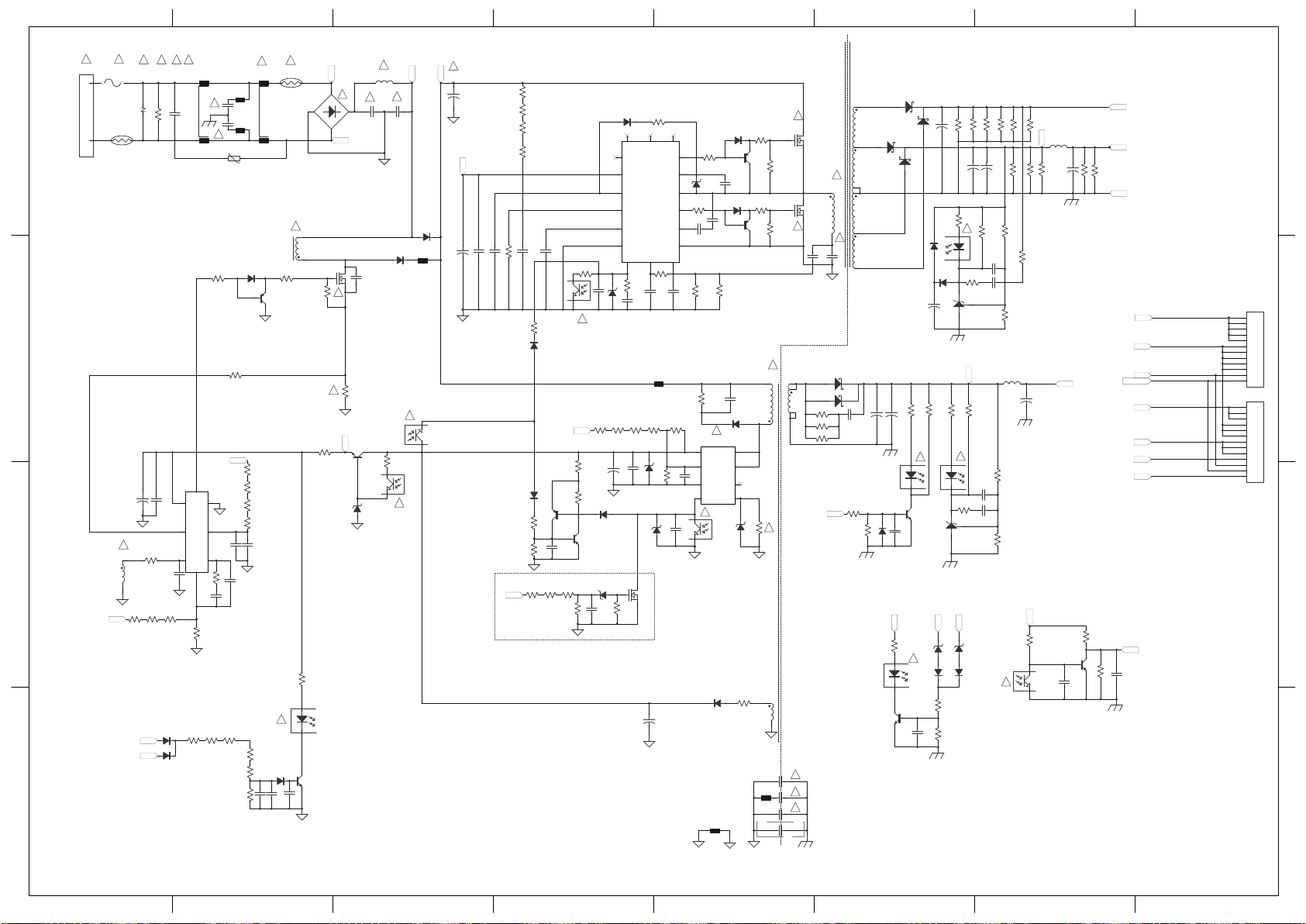
1
1
2
2
3
3
4
4
5
5
6
6
7
7
8
8
D
D
C
C
B
B
A
A
12
PC101:2
24V/2.8A
3 4
PC502:1
34
PC102:1
L201
T101:8
T101:9
T101:10
T101:11
12V4.3A
12
PC102:2
24V
12V
GND
S2
S2
T101:7
SECONDARY
+
C101
T101:2
T101:4
Reg
8
FB
3
N.C.
12
VCC
2
Vsen
1
CSS
5
RC
7
SGND
4
OC
6
VS
15
VGH
16
VB
14
VGL
11
RV
9
PGND
10
N.C.
13
N.C.18N.C.
17
U101
3 4
PC101:1
SSC9502
Vcc
3 4
PC501:1
C505
FB4S/OCP
1
BR
2
Vcc5D
8
D
7
N.C.6GND
3
U501
1 2
FB502
A6069H
PRIMARY
P2
Vcc
P3
BD101
1 2
LF101:1
34
LF101:2
1
2345
678
U601
L601:5
+
C606
P801
12
FB601
L
N
P3
P2
P2
P1
P1
Q602
1 2
LF102:1
34
LF102:2
T101:12
L202
5V/2.5A
S3
12
PC502:2
12
PC501:2
S3
S3
F101
VA101
TH102
CX101
SA101
Q601
R101
R627
R629C611
C610
C612
R630
R604 R605 R606
R621
R623
R624
R625
R626
C607
C608 C609
R601
R602
R603
D602
D101
D601
R102
R103
R104
C105
C106
C112
C113
R133
R121
R122
R123
R124
R125
R126
R127
Q101
Q102
D102
+
C104
C108
C109
C110
D103
D104
C111
C103
C102
C114
C115
C116
R128
R129
ZD101
ZD102
R130
R131
R132
D105
Q103
Q104
R134
R501 R502
R503 R523
C501
R521
R522
ZD501
C506
C507
ZD502
R524
R525
R526
R527
R528
D501
D502
C508
R504
Q501
Q502
R505 R506
R529
C509
ZD503
R530
Q503
R531D503
Q504
ZD504
R532
CY103
+
C201
+
C202
+
C203
R213
R214
D504
+
C204
+
C205
R215
R216
R217
C209
C210
R218
A C
R
U201
R219
R220
R221
C206
R222
R223
R224
R225
R226
C215
C216R230
1 2
3
U202
R231
Q202
C220
D208
R239
R237
R238
R240R241
C221
D209
D210
ZD201
ZD202
Q205
CY101
CY102
+
C504
L601:1
L601:6
L601:8
T501:4
T501:6
T501:7
T501:8
T501:9
T501:10
T501:1
T501:2
CY105
R507
R105
N.C.
R607
CY104
C601
C602
L602
CY106
D205
" "
" " " "
"
"
"
"
"
"
"
"
"
"
"
"
"
"
"
"
"
"
"
"
"
"
"
"
"
"
"
"
"
"
"
N.C.
R242
R243
R244
R245
R246
R247
3 4
PC103:1
R228
C211
ACD
5V
1
2
3
4
5
6
7
8
9
10
11
12
P201
24V
GND
DIM
5V
12V
ACD
BL_ON/OFF
1
2
3
4
5
6
7
8
9
10
11
12
13
P202
PS ON
12
PC103:2
R137
!
R135
D108
D107
C118
R109 R110
R111
C117
R112
R113
Q106
D106
C119
P3
P4
P4
5V
P801:1
P801:4
PS ON
D203
ZD505
D201
R227
!
Q201
R229
C207
+
C212
+
C213
+
C502
R232
R233
R234
R235
R236
D206
D207
+
C214
R631
TH101
12
FB101
1 2
FB102
1 2
FB103
C603
12
FB104
POWER [1]
Page 48

SCHEMATIC DIAGRAM
Стр. 1
из
2
17.
04.
2015
file:///C:/Users/
Александр
/Desktop/32AV703R
-
01/html/c_precaution.html
Precaution
WARNING: BEFORE SERVICING THIS CHASSIS, READ THE "X-RAY
RADIATION PRECAUTION" FOR DIRECT VIEW CTV ONLY, "SAFETY
PRECAUTION" AND "PRODUCT SAFETY NOTICE" OF THIS MANUAL.
CAUTION: The international hazard symbols " " in the schematic diagram
and the parts list designate components which have special characteristics
important for safety and should be replaced only with types identical to those
in the original circuit or specified in the parts list.
The mounting position of replacements is to be identical with originals.
Before replacing any of these components, read carefully the SAFETY
PRECAUTION and PRODUCT SAFETY NOTICE.
Do not degrade the safety of the receiver through improper servicing.
Note:
1. RESISTOR
Resistance is shown in ohm [K=1,000, M=1,000,000]. All resistors are 1/6 W and 5 %
tolerance carbon resistor, unless otherwise noted as the following marks.
Metal or
1/2R :
1/2S :
1RF :
10
W
K : ±10 %
G : ±2 %
F : ±1 %
2. CAPACITOR
Unless otherwise noted in schematic, all capacitor values less than 1 are expressed in µF,
and the values more than 1 in pF.
All capacitors are ceramic 50 V, unless otherwise noted as the following marks.
Metal oxide
of 1/2 watt
Carbon
composition
of 1/2 watt
Fuse resistor
of 1 watt
Cement of
:
10 watt
Electrolytic
=
capacitor
Mylar
=
capacitor
Page 49

3. The parts indicated with " " have special characteristics, and should be replaced with
Стр. 2
из
2
17.
04.
2015
file:///C:/Users/
Александр
/
Desktop/32AV703R
-
01/html/c_precaution.html
identical parts only.
4. Voltages read with DIGITAL MULTI-METER from point indicated to chassis ground,
using a color bar signal with all controls at normal, line voltage at nominal AC volts.
5. Waveforms are taken receiving color bar signal with enough sensitivity.
6. Voltage reading shown are nominal values and may vary ±20 % except H.V.
Page 50

.(< 0$,1 32:(5 3$1(/
&21 &1 3 &1/7$$3 &1/7$$3
*1' 3$1(/B9&& 9 1& 9
*1' 3$1(/B9&& 9 1& 9
.(< 3$1(/B9&& 9 1& 9
.(< 3$1(/B9&& 9 *1' 9
2'B6(/ 9 5;,1 9
3$1(/B9&& *1' 5;,1 *1'
5;( *1' *1' *1'
*1' *1' 5;,1 *1'
5;( *1' 5;,1 *1'
5;( *1' *1' *1'
5;(& ',0 5;,1 (5525287
,5B/(' 5;( %B2) 5;,1 EDFNOLJKWRQRII
*1' *1' GLPPLQJFRQWURO
&1 &1 5;(& &1 3 5;&/. 1&
9B67%< 9B67%< 5;( 9 9 5;&/.
*1' *1' *1' 9 9 *1'
5&B,5 *1' 5;( 9 9 5;,1
*1' *1' 5;( *1' *1' 5;,1
/('B21B2)) *1' 5;( *1' *1' *1'
/('B7,0(5 .(< 5;( *1' *1' 1&
.(< *1' 9B67%< 9 /9'6237,21
*1' 5;( 9B67%< 9 1&
5&B,5 5;2 9B67%< 9 *1'
/('B21B2)) *1' $&'HWHFW $&' *1'
/('B7,0(5 5;2 %5,*+7B$'-B3:0 ',0 1&
5;2 %5,*+7B$'-B'& %B2) 9,1
5;2& ,19(57(5B21B2)) 36B21 9,1
5;2 67$1'%< 3 9,1
*1' /,1( 9,1
5;2& 1(875$/ 9,1
5;2
*1'
5;2
5;2
5;2 &1
5;2 63.B5
*1' 63.B5
5;2 63.B/
3$1(/B6 63.B/
3$1(/B6
/
5
Page 51

PARTS LIST
Стр. 1
из
1
17.
04.
2015
file:///C:/Users/
Александр
/Desktop/32AV703R
-
01/html/lst_precaution.html
Precaution
WARNING: BEFORE SERVICING THIS CHASSIS, READ THE "SAFETY
PRECAUTION" AND "PRODUCT SAFETY NOTICE".
CAUTION: The international hazard symbols " " in the schematic diagram
and the parts list designate components which have special characteristics
important for safety and should be replaced only with types identical to
those in the original circuit or specified in the parts list.
The mounting position of replacements is to be identical with originals.
Before replacing any of these components, read carefully the "SAFETY
PRECAUTION" and "PRODUCT SAFETY NOTICE".
Do not degrade the safety of the receiver through improper servicing.
Note:
• The part number must be used when ordering parts, in order to assist in processing, be
sure to include the Model number and Description.
• The PC board assembly with mark is no longer available after the end of the
production.
Abbreviations
Capacitors CD : Ceramic Disk
Resistors CF : Carbon film
OMF : Oxide Metal Film
PF : Plastic Film
CC : Carbon Composition
VR : Variable Resistor
EL : Electrolytic
MF : Metal Film
FR : Fusible Resistor
All CD and PF capacitors are ±5 %, 50 V and all resistor, ±5 %, 1/6 W unless otherwise
noted.
 Loading...