

Page 1
R6000 CAT. 1 CHASSIS
VIDEO RECORDERS
19, AVENUE DUBONNET - B.P.25
92403 COURBEVOIE CEDEX
TEL.(1) 46 91 36 00 -
TELEX : 610 081 F - TELECOPIE : (1) 46 91 01 80
Code : 350 543 90 - 1295/00 M - 000 000 - Imp.
Tous droits de reproduction, de traduction, d'adaptation Les descriptions et caractéristiques figurant sur ce document sont données à titre d'information
et d'exécution réservés pour tous les pays. et non d'engagement. En effet, soucieux de la qualité de nos produits, nous nous réservons
le droit d'effectuer, sans préavis, toute modification ou amélioration.
S.A. AU CAPITAL DE 200 000 000 F
SIEGE SOCIAL : 9, Place des Vosges - La Défense 5
92400 COURBEVOIE
RCS NANTERRE B 322 019 464
TECHNICAL GUIDE
Page 2

R6000 MONO
CHASSIS VIDEO
RECORDERS
TECHNICAL GUIDE
Centre de formation
46 Quai Alphonse Le Gallo
92648 BOULOGNE CEDEX
Tél :0141865000
N° de déclaration d'existence :
1 1 92 052 87 92
Tous droits de reproduction, de traduction, d'adaptation Les descriptions et caractéristiques figurant sur ce document sont données à titre d'information
et d'exécution réservés pour tous les pays. et non d'engagement. En effet, soucieux de la qualité de nos produits, nous nous réservons
le droit d'effectuer, sans préavis, toute modification ou amélioration.
Siège Social
46 Quai Alphonse Le Gallo
92648 BOULOGNE CEDEX
S.A. au capital de 200.000.000 francs
R.C.S Nanterre B 322 019 464
Code :000000000 - 01/97 M - 000 000 - Imp.
Page 3

R6000
CAT. 1
CHASSIS VIDEO
RECORDERS
Page 4

Page 5

1
CONTENTS
INTRODUCTION 3
SETUP MORE 11
POWER SUPPLY 17
MECANISM 31
SERVO CONTROL 37
PROGRAMMIG OSD 51
SERVO CONTROL 61
SWITCHING 79
VIDEO PROCESSING 85
Page 6

2
Page 7

3
INTRODUCTION
Page 8

4
Page 9

5
The chassis and commercial model numbers of 6000 Series video recorders are as follows:
CHASSIS MODEL NO.
R6015CE
R6045CE
R6048CE
R6414CE
R6444CE
R6704PS
R6744PS
COMMERCIAL MODEL
VP2750
VP4750
VP4780
VR8027
VR8047
VK231PS
VK431PS
THOMSON
SABA
BRANDT
EXPLANA TION OF CHASSIS MODEL NUMBERS
R: Video recorder
First digit: Series to which device belongs (in this
case, 6 = 6000 Series)
Second digit: Brand of device
0: Thomson
4: Saba
7: Brandt
Third digit: Product type
0: Two video heads, basic
1: Two video heads
4: Four video heads
Fourth digit:
4/5: ShowView
8: ShowView, Jog Shuttle
CE: Central Europe (BG, DK, L)
PS: PAL/SECAM
BRAND
Page 10
6
NO
NO
YES
CHARACTERISTICS
NUMBER OF VIDEO HEADS
H. Q.
CASSETTE TIME AND "TAPE
REMAINING" COUNTER
REAL-TIME TAPE
COUNTER
DIRECT ACCESS
INDEX: MARKING/SEARCH
FWD/REW VISUAL SEARCH
5 speeds
IMAGE PAUSE, FRAME-BY-FRAME,
SLOW MOTION
OPEN-ENDED
RECORD/PLAY
AUTOMATIC AV
RECORDING
COLLISION MESSAGE
PICTURE PEAK ADJUSTMENT
SATELLITE RECEIVER CONTROL
PLAY NTSC ON PAL TV
Automatic channel name memory
VP2750
VR8027
VK231
VP4750
VR8047
VK431
2
YES
WH. C/DE/YNR
YES
NO
YES
NO
NO
NO
YES
NO
4
WH. C/DE/YNR
YES
YES
NO
NO
YES
YESYES
NO
YES
NO
NO
NO
YES
NO
LONG PLAY NO YES
VP4780
4
WH. C/DE/YNR
YES
YES
YES
YES
YES
YES
YES
YES
YES
YES
YES
YES
YES
YES
Page 11
7
CHARACTERISTICS
UHF MODULATOR
VK231
VK431
VR8027
VR8047
VP2750
VP4750
VP4780
L
51 through 67
L ,G, K
51 through 67
L ,G , K
51 through 67
WIDE BAND TUNER YES YES
YES
CHANNEL SEARCH
SYNTH. FREQ.
99 PRG.
SYNTH. FREQ.
99 PRG.
SYNTH. FREQ.
99 PRG.
STANDARDS LL’BG LL’BGDKK’ LL’BGDKK’
COLOUR STANDARD
PAL SECAM
MESECAM
PAL SECAM
MESECAM
PAL SECAM
MESECAM
AUTO CHANNEL MEMORY
YES YES YES
CHANNEL CLASSIFICATION NO YES YES
OSD ON TV YES YES YES
AUTO TIME SET NO YES YES
PROGRAMMING 8 progs. over 1 year 8 progs. over 1 year 8 progs. over 1 year
VPS / PDC NO YES YES
SHOWVIEW YES YES YES
VIDEO CAMERA SYNCHRO MOUNTING NO NO YES
MAINS POWER CUT BACKUP 30 mn 30 mn 30 mn
FRONT PANEL AV CONNECTORS NO NO YES
TV Universal REMOTE CONTROL UNIT NO NO YES
A/B CODE NO NO YES
Page 12

8
Page 13

9
LANGUAGE SELECTION
Press and hold the EXIT/STATUS key on the remote control unit for a few seconds. "French"
and "English" are displayed in turn. Release the key to make your selection.
UHF MODULATOR CHANNEL ADJUSTMENT
Connect the antenna cable to the antenna system.
Press and hold the A menu key until SYS appears on the video recorder display.
Use the AV key to select the system.
SYS 1 France (L standard)
SYS 2 Western Europe (BG standard)
SYS 3 Eastern Europe (DK standard)
Press <A> to continue.
After a few seconds, the video recorder shows the channel number. You can change it using
the + and - keys on the remote control.
OPERATING TIME
Press and hold the 0000 or ERASE key on the remote control for ten seconds. A menu
appears on the screen, and shows the number of hours of operating time in Play Mode and
Record Mode.
Page 14

10
Page 15

11
SETUP MODE
AND
SELF DIAGNOSIS
Page 16
12
Com. Ref.
VP2750
VP4750
VP4780
VR8027
VR8047
VK231PS
VK431PS
1
0
0
0
0
0
0
0
3
1
1
2
1
1
0
0
4
0
0
0
0
0
0
0
5
8
8
8
8
8
8
8
6
4
E
E
4
E
4
E
7
4
4
4
0
0
0
0
8
4
4
5
4
4
4
4
9
B
B
B
B
B
4
4
10
0
0
0
0
0
0
0
11
9
9
B
9
9
1
1
12
1
1
3
1
1
1
1
13
0
8
A
0
8
0
8
14
3
3
3
3
3
B
B
Model
R6015CE
R6045CE
R6048CE
R6414CE
R6444CE
R6704PS
R6744PS
2
2
2
2
2
2
1
1
TABLE OF R6000 SETUP MODE CODES
Page 17

13
SETUP MODE
GENERAL RESET
- Disconnect the video recorder from the power supply.
- Press <P+> and <P-> on the keypad. For a machine without these keys, press
<Stop>, <Play>, and <Standby> on the keypad.
- Reconnect the video recorder to the power supply, and release the keys.
The Setup consists of 14 digits corresponding to the Setup mode values.
In Setup mode, certain values can be entered according to the characteristics of the device
(see summary table).
DATA ENTRY
The digit to be confirmed flashes on screen. Use the number keys on the remote control to
make entries or changes.
Press <2> to go to the next digit. Press another number key to change the value from 0 to F.
Note: Before storing the parameters in memory, it is essential to go back to the first digit.
MEMORY
Press <Stop> on the remote control or keypad.
You can quit the menu without entering anything in the memory by pressing <Exit> or <Off>.
SETUP
0 2 1 0 8 4 4 4 B 0 9 1 0 3
STOP
store
Page 18

14
Digit Number Meaning Value
1 and 2 Function requested and position 1 - Fast FWD or REW
of mechanism at the time of the 2 - Stop
incident 3 - Stanby
3 - Play
4 - Reverse play
5 - Load/Unload
6 - Arrêt (unload at limit stop)
7 - Eject.
F - Initialisation
3 and 4 Function performed by the 00 - Stop
microprocessor (Servo control/ 01 - Fast rewind
Automatic control) 02 - Fast forward
04 - Play
11 - Reverse play
12 - Search/Play
44 - Record
84 - Image pause
C4 - Record pause
40 - Record/Record pause
10 - Search
5,6,7 and 8 Function in progress before error bit 0
Normal 0 0 0 0
Record 0 0 0 1
FRAME-BY-FRAME 0 0 0 4
Stop (unload at limit stop) 0 0 0 8
Eject. 0 0 1 0
Stop 0 0 2 0
Capstan lock 0 0 4 0
Initialisation 0 0 8 0
Record loop 0 2 0 0
Play loop 0 4 0 0
Record or play loop 0 8 0 0
Fast FWD or REW 1 0 0 0
Search 2 0 0 0
Image pause 4 0 0 0
Play 8 0 0 0
9 and 10 Error message 81 - Drum
82 - Left reel stand
84 - Right reel stand
88 - Function incomplete
Page 19

15
SELF DIAGNOSIS
STOP
EXIT
clear number
exit
00 00 00 00 00
SELF DIAGNOSIS
When a mechanical incident occurs, or following an operator error, a 10-digit number
representing the error is stored in the EEPROM. This number can be displayed on screen so
that the problem can be investigated and solved.
ERROR MESSAGE DISPLAY
There are two ways to do this:
Via Setup mode, when the Service Setup page is displayed on screen, press the Fast
Forward key on the remote control.
In Stop or Standby Mode, when nothing is displayed on the television screen, press
<ERASE/0000> for at least ten seconds.
Use the table opposite to interpret the message.
ERASE THE TEN DIGITS OF THE ERROR MESSAGE
Press <Stop> on the remote control.
EXIT SETUP MODE WITHOUT STORING IN MEMORY
Press <Exit> on the remote control.
SERVICE COUNTER
Page 20

16
Page 21

17
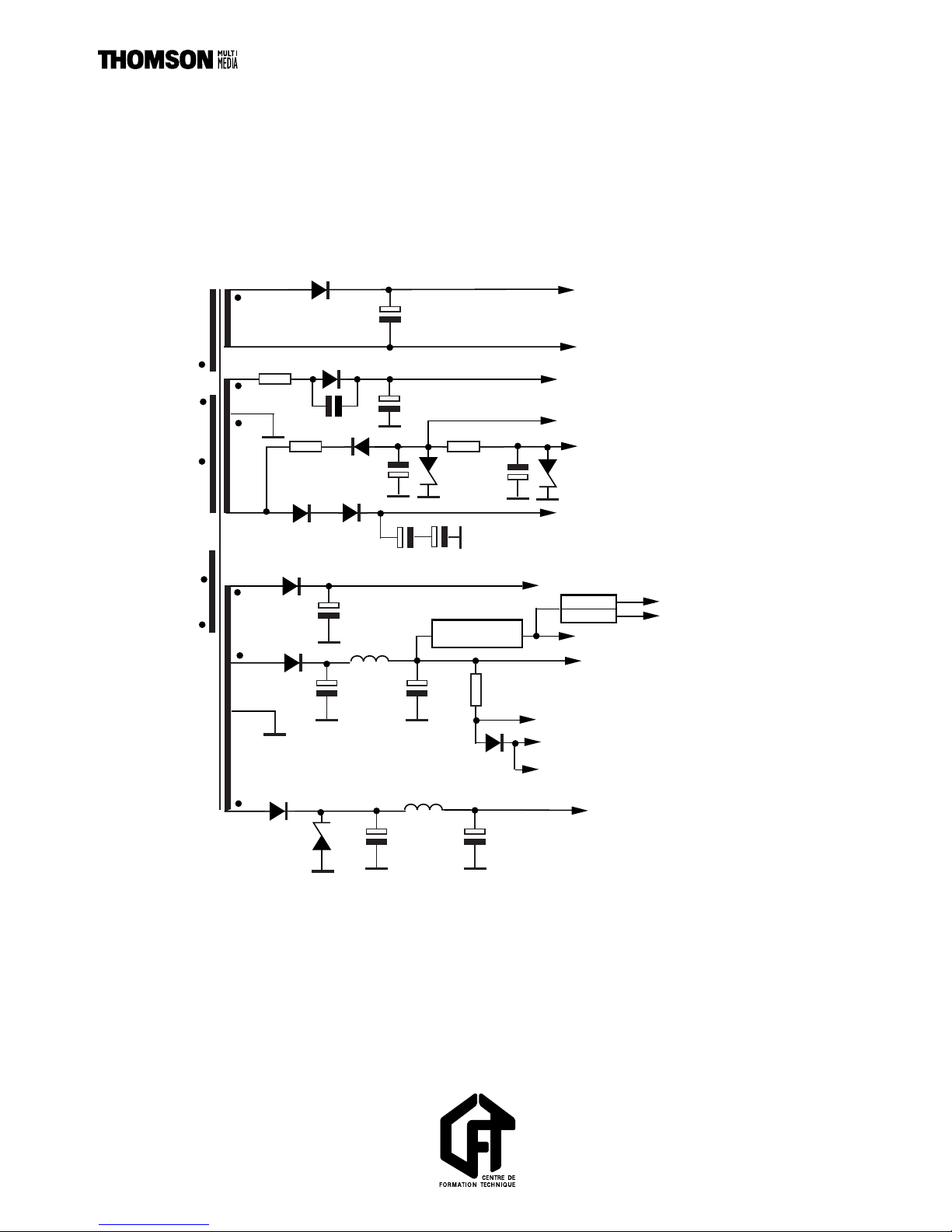
POWER SUPPLY
Page 22
18
CP023
RP024
CP024
RP019 DP019
RP021
RP022
RP029
TP023
TP020
CP021
RP026
TP022
CP022
RP020
RP027
RP025
CP025
DP025
RP037
DP037/ 038
RP038
CP038
DP023
RP023
RP004/005/006
007/008/009
FP44
CP010
DP002
DP003
DP001
DP004
300V
4
6
5
8
3
9
1
RP028
7
RP012
DP012
DP041
DP040RP041 RP040
CP040
SECONDARY
REGULATION
IP 050
5 VE
14 VE
DP033
CPO31/ 032
DP034
DP031
RP033
RP034
RP011
DP005
DP044
DP020
LP050
3,9 V
33 V
22 V
6,8 V
Page 23

19
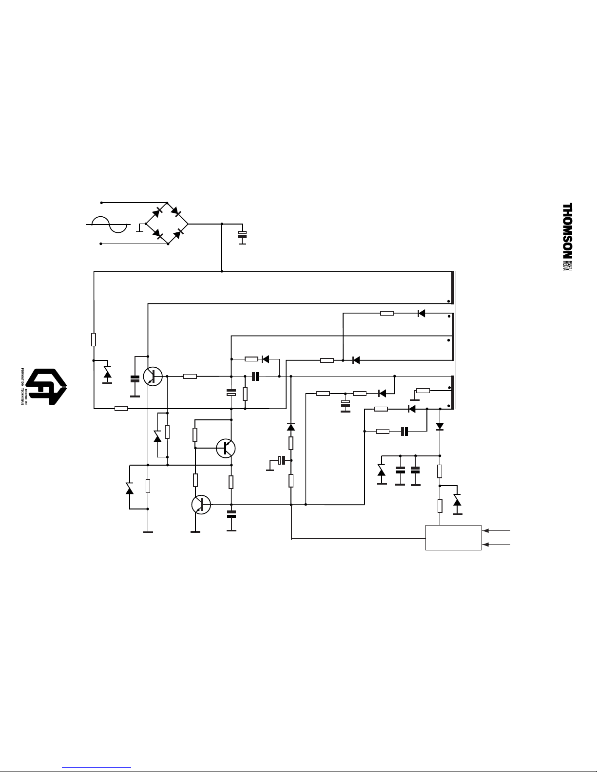
GENERAL INFORMATION
Self-oscillating switching power supply called FROSIN (FRee Oscillating Safe INtelligent).
In operation, the switching frequency varies from 42 kHz to 45 kHz for a power of 17 W . In
Standby Mode, the switching frequency is close to 56 kHz for a power of 9 W . In Standby there
is a Power-Saving Mode, where the frequency is 23 kHz and consumption is 4.8 W .
CONDUCTION OF SWITCHING DEVICE TP20
The 300 V dc voltage, rectified and filtered by DP01 through DP04 and CP10, is used as a
source for start-up. It supplies the base current for TP20 via RP04/05/06/07/08/09/1 1,
CP23/RP24 and RP21.
The current induced in winding 4-6 of LP050 via DP19/RP19 maintains conduction in TP20.
CP24 accelerates the conduction of TP20.
While TP20 is conducting, CP23 is charged by winding 8-3 of LP050 via DP23 and RP23.
LOCKING OF SWITCHING DEVICE TP20
When the voltage at the terminals of RP20 is suf ficiently high, TP22 conducts, followed by
TP23. CP23 is then connected between the base and emitter of TP20, and leads to its
discharging and locking. A polarity reversal at the terminals of LP050 achieves the following:
- Improved discharging by CP24
- Recovery of the energy in the secondaries
- Putting into service of the regulation
- Charging of CP25 via DP25 (soft start circuit)
- Maintaining conduction of TP22/23 via DP37/38 and RP37 (FROSIN circuit)
- Maintaining the charging of CP023 by 7 of LP050, DP12, RP12, and 3 of LP050.
SOFT START
The negative voltage, rectified by DP25 and filtered by CP25, delays the instant of conduction
of TP22/23, and then the instant at which TP20 locks. At first, this negative voltage is 0. TP22
commands come from RP20. This negative voltage then appears and increases, and then
delays control of TP22/23. The conduction time of TP20 is therefore increasingly long.
Page 24
20
CP023
RP024
CP024
RP019 DP019
RP021
RP022
RP029
TP023
TP020
CP021
RP026
TP022
CP022
RP020
RP027
RP025
CP025
DP025
RP037
DP037/ 038
RP038
CP038
DP023
RP023
RP004/005/006
007/008/009
FP44
CP010
DP002
DP003
DP001
DP004
300V
4
6
5
8
3
9
1
RP028
7
RP012
DP012
DP041
DP040RP041 RP040
CP040
SECONDARY
REGULATION
IP 050
5 VE
14 VE
DP033
CPO31/ 032
DP034
DP031
RP033
RP034
RP011
DP005
DP044
DP020
LP050
3,9 V
33 V
22 V
6,8 V
Page 25

21
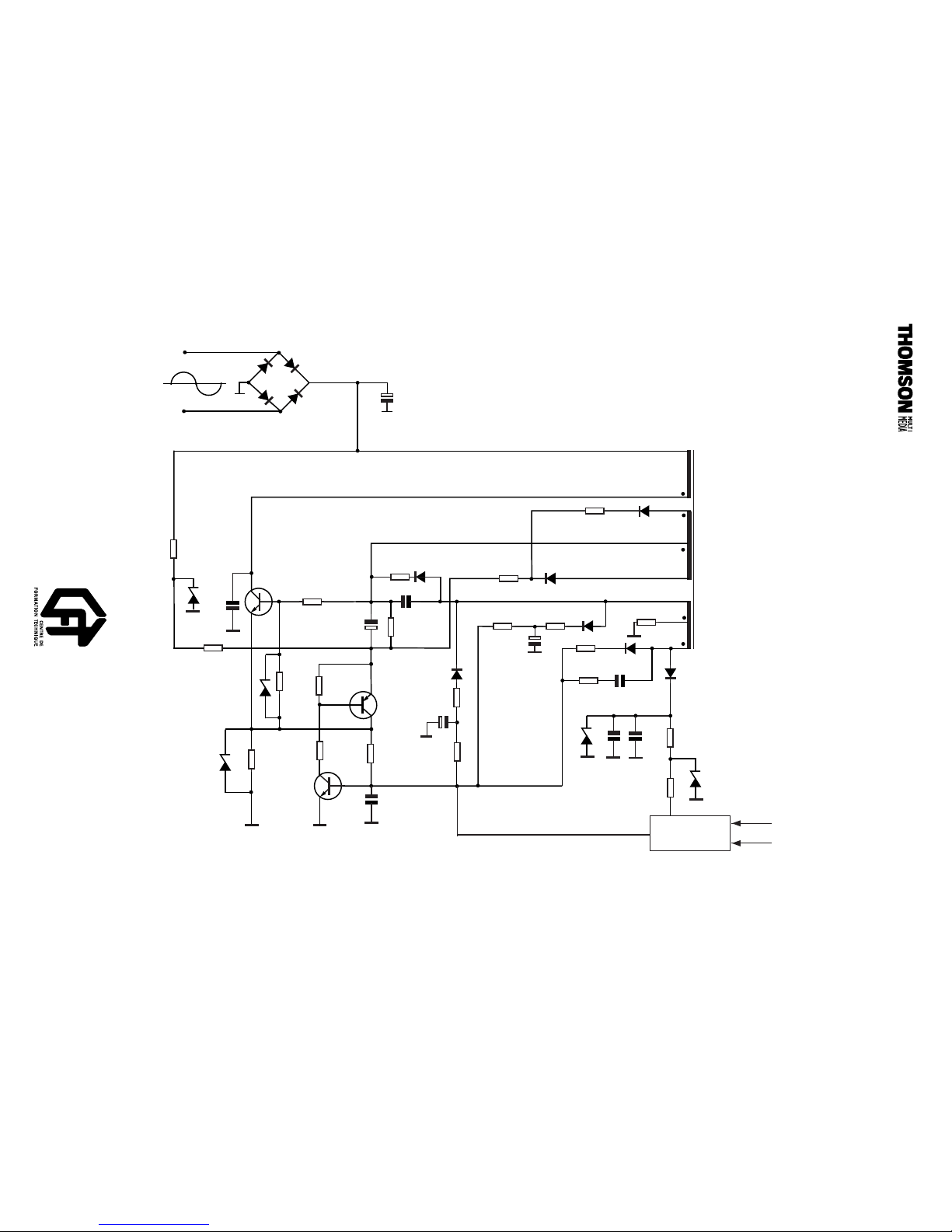
FROSIN CIRCUIT
During the energy restoration phase, Transistors TP22/23, maintained in their conduction
phase by Network 5 of LP050, DP37/38, and RP37, block TP20. At the end of
demagnetisation, the voltage induced on the collector of TP20 is reduced, and the charging of
CP21 triggers an oscillation cycle with the primary of LP050. Because of this, the collector
voltage of TP20 continues to fall when it reaches 300 V.
The new saturation control of TP20 becomes involved when the collector voltage of TP20 is
close to 0. This effect is obtained by placing a time delay on the action of the positive voltage
induced at 4 of LP050. This limits power losses due to the switching of TP20. The efficiency of
this power supply is therefore above 81% in operation (38% in Standby Mode).
This time delay is caused by the time taken to discharge TP22/23 (related to the FROSIN
circuit: DP37/38, RP37 by controlling the saturation current).
POWER SUPPLY BEHAVIOUR IN STAND-BY MODE
Because the secondaries require little energy in Stand-by Mode, the saturation time of TP20
tends to fall to 0.2 µs (frequency on the order of 200 kHz). This value is too low, and would
affect power supply efficiency in this mode. A minimum conduction time circuit (Ton min =
0.5 µs) for TP20 has therefore been added, using components CP38/RP38.
In steady state, regulation phototransistor IP050 cannot handle the saturation of TP22 and
TP23 (and then the blocking of TP20) alone. The following must assist:
• Positive voltage produced at RP20 terminals during the Storage Phase,
• Positive voltage supplied by the FROSIN circuit (DP37/38) in Restoration Phase.
In Standby Mode, the stored energy becomes greater than the small requirements of the
secondaries. Because of this, the secondary voltages, and in particular the 14 V, increase
during the energy restoration phases. The conduction time of TP20 is shortened to 3 µs by the
secondary regulation effect. This limits the energy stored in LP050.
Ton min is a result of the negative pulse obtained from the voltage induced in 5 of LP050
(negative when TP20 is conducting) and the charging of CP38 via RP38. This negative pulse
keeps TP22 blocked for a minimum of 0.5 µs.
Page 26
22
CP023
RP024
CP024
RP019 DP019
RP021
RP022
RP029
TP023
TP020
CP021
RP026
TP022
CP022
RP020
RP027
RP025
CP025
DP025
RP037
DP037/ 038
RP038
CP038
CP071
CP041
DP023
RP023
RP004/005/006
007/008/009
FP44
CP051
DP051
DP056
CP057
CP056
DP061 CP061
CP010
DP002
DP003
DP001
DP004
300V
4
6
5
11
8
14
7
10
9
1
RP028
3
RP012
DP012
DP041
DP040RP041 RP040
CP040
DP033
CPO31/ 032
DP034
DP031
RP033
RP034
RP073
RP035
RP073
RP067
RP065
RP011
DP005
DP044
DP020
16
17
+ UH
- UH
RP056
+ 33 VE
18
CP054
DP053
RP053
- 30 VE
DP081/ 082
CP081/ 082
+ 36 VE
VM + 20VE
15
1
6
2
5
4
14VE
13
5VE
DP067
CP064
CP068
CP066
CP067
CP065
CP064
DP064
DP066
DP071
TP071
DP073
4V3
IP050
DP067
LP066
12
13,6 VEDM
13 VECM
13 VELM
RW085
DW086
DP054
DW010
CW004
RW005
- 5 VE
LP050
22V
6,8V
3,9V
33V
Page 27

23
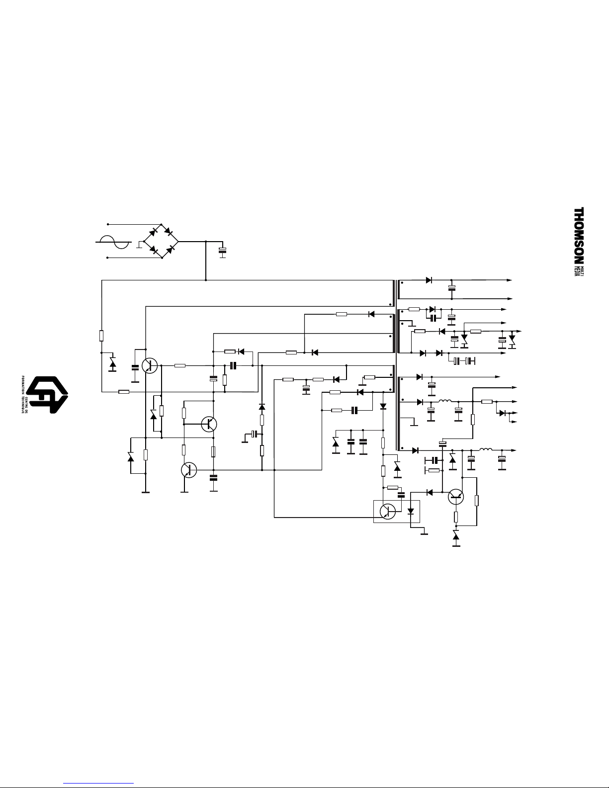
SECONDARY REGULATION
Transistor TP071 and optocoupler IP050 are used in conjunction for secondary regulation. The
current in the optocoupler diode is controlled by the regulation error voltage from the collector
of TP071. (This error voltage is obtained by comparing a reference voltage on the base of the
transistor and the 5VE image).
This current sets the value of the internal resistor in the optocoupler transistor. The switching
transistor is blocked according to the addition of the voltage obtained at the terminals of
Resistor RP020 and the voltage brought back by the internal resistor of the optocoupler
transistor. These two voltages polarise the base of TP022.
CP068 allows IP050 to handle abrupt variations of 14VE (motor start-up).
SECURITY
To avoid security problems, a new component called Protector Module (e.g. FP044) has
replaced classic fuses in several positions.
The advantage of the Protector Module is the ratio between its maximum current and the
current that destroys it. This ratio is 3, whereas the ratio is greater than 15 for a classic fuse.
In the event of an excessive increase in the conduction time of Transistor TP20 (overload of a
secondary), the voltage induced on winding 4-6 of LP050 during this phase increases and
charges Capacitor CP040. From a certain threshold, this will saturate TP022, block TP020,
and therefore shut off the power supply until CP040 discharges and allows TP022 to be
become blocked to re-start the power supply.
Page 28
24
CP051
DP051
DP056
CP057
CP056
DP061 CP061
4
6
5
11
8
14
3
10
9
1
7
16
17
+ UH
- UH
RP056
+ 33 VE
18
CP054
DP053
RP053
- 32 VE
DP081/ 082
CP081/ 082
+ 36 VE
VM + 20VE
15
14 VE
13
5VE
DP067
CP064
CP066
CP067
CP065
CP064
DP064
DP066
LP066
12
DP054
DW010
CW004
RW005
- 5 VE
ON / OFF
FROM PIN
24 IR001
ECO
CP095
DP096
DP097
RP096
RP094
RP095
RP098
TP095
TP096
_____
Page 29

25
ECO CIRCUIT
This circuit reduces consumption in Standby Mode from 9 W to 4.8 W by shutting off the display
and replacing it with a red LED on the front panel. Two transistors (TP095 and TP096) are
used to perform this function. In classic Standby Mode, these two transistors are blocked.
This function is enabled by Line 7 of the main menu, which supplies a Level 1 to Pin 24 of the
control microprocessor during the changeover to Standby Mode. This saturates the two
transistors.
The saturation of these transistors damps Transformer LP050, leading to a reduction in
frequency, to 23 kHz, and a reduction of the energy storage time. Because of this, all the
voltages fall, which limits consumption by eliminating the display.
Only the 5VE voltage remains at its nominal value because of the regulation.
Page 30
26
CP051
DP051
DP056
CP057
CP056
DP061 CP061
11
14
10
16
17
+ UH
- UH
RP056
+ 33 VE
18
CP054
DP053
RP053
- 30 VE
DP081/ 082
CP081/ 082
+ 36 VE
VM + 20VE
15
14VE
13
5VE
DP067
CP064
CP066
CP067
CP065
LP064
DP064
DP066
LP066
12
13,6 VEDM
13 VECM
13 VELM
RW
085
DW086
DP054
DW010
CW004
RW005
- 5 VE
LP050
12 VS
5 VS
5 VS
TW 083
DT 067
TW001 -TW002
TW003 - DW006
( SERVO CONTROL)
Page 31

27
SECONDARY VOLTAGES
The energy exchange caused at the primary induces several secondary voltages.
Pin 16/17 via DP051, CP051: two voltages, +UH and -UH, to supply power to the display
filament.
Pin 10 via RP056, DP056, CP057: a 33VE voltage used to obtain the Varicap voltage for the
tuner.
Pin 18 via RP053, DP053, CP054, stabilised by DP054: -30 V for the display grid, and then
stabilised by DW010: a -5VE voltage used to power the switching stages.
Pin 18 via DP081, DP082, CP081, CP082: a +36VE voltage used for the POWER GOOD
function.
Pin 11 via DP061, CP061: a +20VE VM voltage used to over-supply the capstan motor for the
REWIND function.
Pin 15 via DP064, CP064, LP064, CP065: a 14 VE voltage. This voltage is used to obtain
three voltages to supply power to the motors:
-13.6 VEDM for the drum motor,
-13 VELM for the function control motor and slow switching of AV1
-13 VECM for the capstan motor.
This voltage also obtains the 12VS switched voltages via TW001, TW002, TW003, and DW006
for the tuner and the IF, and two 5VS voltages. The first polarises Pin 80 of IT001 via Zener
diode DT067. The second powers the HF and IF stages, video processing, audio processing,
and switching via TX083.
Pin 12 via DP066, CP066, LP066, CP067, stabilised by DP067: a 5VE voltage supplying
power to the control and programming stages, the tuner, and the switching.
Page 32

28
140 V
120 V
0
0,9V
-6 V
0,17 V
-0,25 V
1 V
-0,2 V
0
0
0
10 s
46 s
63 s
TP20
COLLECTOR
TP20
BASE
TP20
EMITTER
TP22
BASE
-6 V
1,3 V
Page 33

29
POWER SUPPLY TROUBLESHOOTING METHOD
POWER SUPPLY CHECK USING THE LOW-VOLTAGE METHOD
• Discharge Capacitor CP10
• Shunt Resistors RP004 through RP011 using a 10kΩ resistor.
• Power the video recorder with 12 V dc via the mains connector.
In this configuration, the following measurements are obtained on the secondaries:
DP056 cathode (33 V) : 11 V
DP053 anode (-32 V) : -10 V
DP061 cathode (20 V) : 7 V
DP064 cathode (14 V) : 5.4 V
DP066 cathode (5 V) : 2.1 V
Page 34

30
Page 35

31
MECHANISM
Page 36

32
The mechanism has three motors:
Drum motor (three-phase ac).
- The stator of this motor is secured to the chassis.
- Capstan motor
- Function control motor.
Functions of the Capstan Motor:
- Sets the tape winding speed,
- Drives the reel stands via a belt and a free wheel.
Functions of the Function Control Motor:
- Cassette loading and ejection,
- Loading and unloading of tape,
- Positioning of the mechanism parts.
Page 37

33
CASSETTE LOADING
Microcontactor ST001 on the Main Board handles cassette detection. This microcontactor is
actuated by the front left cam of the cassette holder, and closes when a cassette is inserted.
The function control motor is powered, and drives the cassette holder drive axle via the
cassette holder control slide and control cam.
When cassette loading is complete, and after an analysis of drum motor and capstan motor
rotation, the function control motor loads the tape using its control cam.
NOTE: If the drum position and speed signal is absent, the tape is not loaded. Loading does
take place, however, if the Stop function is requested. If signals FGA and FGB are absent, the
tape is not loaded, and the cassette is ejected.
The tape start and tape end phototransistors and the mechanism position switch indicated
whether or not a cassette is present in the device.
- Tape start phototransistor blocked: 5 V at 50 of IT001
- Tape end phototransistor blocked: 5 V at 52 of IT001
- Cams A, B, and C must not indicate the EJECTION code (0 on Pins 9, 10, and 11 of
IT001).
TAPE LOADING AND POSITIONING OF MECHANISM PARTS
The control cam and its associated mechanisms load the tape and position the parts of the
mechanism.
In addition, a switch analyses control cam movement, and then informs the servo control of the
mechanism's position via the Cam A, B, and C signals.
OPERATION OF MECHANISM WITHOUT CASSETTE HOLDER
- Remove the cassette holder
- Apply power to the video recorder
- Mask the tape start and tape end phototransistors
- Tip the cassette holder drive axle towards the rear (drum).
Page 38

REPLACEMENT OF CONTROL CAM
The part references shown come from the mechanism manual.
DISASSEMBLY
- Remove the function control motor assembly by releasing the four clips (mechanism manual,
Page 10).
- Remove the cassette holder drive axle (14).
- Remove the right gear of the drive axle (14) by pressing A.
- Remove the drive axle (14) by pulling upwards.
- Remove slide (40) as follows:
- Remove the spring (39),
- Release the levers on each side of the take-up reel stand from the slide (take-up reel
secondary brake lever, and end-of-unloading tape tension lever), and then push the slide
to the right,
- Remove the slide (40).
- Remove the lever (25),
- Remove the capstan idler (1),
- Remove the control cam.
34
A
Marking hole H2
Right gear
shaft 14
Arm 24
Align
Mark
Page 39

35
REASSEMBLY
- Place the loading arm and tape tensioning arm in unloaded tape position.
- Align Guide Hole H2 of Rod 24 with the hole in the chassis.
- Install the control cam by aligning its guide hole (H1) with the hole in the chassis.
- Reinstall the capstan idler by inserting its control tappet in the first cam groove from the axle.
- Reinstall the lever (25) by inserting its tappet in the second cam groove from the axle.
- Reinstall the slide (40). Pay attention to the tape tensioning arm return lever; place its control
tappet in the slot in the slide. Bring the slide over to the left.
- Reinstall the spring (39).
- Reinstall the drive axle (14), and tilt forward.
- Reinstall the drive axle (14) gear, and align as shown below.
A
Marking hole H2
Right gear
shaft 14
Arm 24
Align
Mark
Page 40

36
Page 41

37
SERVO CONTROL
Page 42

38
Page 43

39
GENERAL INFORMATION
The servo control system consists mainly of microcontroller IT001: TMP90PR74.
Keypad function data are generated by programming microcontroller IK01.
The servo control microcontroller is continually informed about mechanism operation by the
static and dynamic status data. These data allow the microcontroller to decide whether to
execute or reject an order.
The servo control microcontroller controls the following via interfaces:
- Capstan motor,
- Function control motor,
- Switching.
In addition, the servo control microcontroller/IT001 automatic control informs programming
microcontroller IK01 to inform the user of the following:
- Cassette presence,
- Cassette type,
- Tape remaining,
- Tape counter reading.
Page 44

40
IT001
IT005
5 V
14VE
33VE
RT072
CT049
TW003
TW002
TW001
RW003
DW006
12 V
DW007
DTO67
5 V
60
64
45
59
80
30
61
13
QT003
16MHz
12 VS
5 VS
ON: 5 V
RESET
AVCC2
1
2
3
1,5Vcc
LT001
RT073
AVCC1
5 VD
TW005
RW009
RW010
TW004
CW002
RW012
RW030
RW006
RT017
RT018
RW002
RW007
RT067
CT049
CW003
33 VE
CT053
DT013
RT081
0,1F
CT032
14
DVCC1
DVCC2
RT072
RT075
TW006
DW015
RW004
RW083
RW084
+ 5VE
5 VS
TW083
CW020
IF, RF
Vid o, Audio,
Switching
Tuner, IF
5 VE
Page 45

41
POWER SUPPLY, CLOCK, RESET, POWER SUPPLY BACK-UP
Power supplies to IT001 are obtained from the 33VE and 5 V from the power supply. A pseudothyristor assembly, TW005, TW004, and a transistor, TW006, allow IT001 to be powered at 5 V.
- 5 VD, Pin 13
- DVCC1, Pin 14
- DVCC2, Pin 64
- AVCC1, Pin 45
Pin 80 of IT001 also receives a switched 5 V voltage (AVCC2). This voltage is present in ON
Mode only.
If one of the power supply tensions of IT001 is missing, Diode DW005 blocks the pseudothyristor assembly, and all power supplies to IT001 disappear.
The signal shaping circuit, IT005, and the time constant of RT072/CT049 reset IT001. The
trigger threshold is 3.2 V.
A 16-MHz clock, 1.5 Vpp, is present at 60 of IT001.
Page 46

42
IK01
C
TIMER
IT001
C
SERVO CONTROL
KEYBOARD
FUNCTIONS
IR/RECEPT.
71
72
73
67
70
21
19
95
97
48
KEYBOARD CTL BUS
CK
K DATAS
REMOTE CONTROL CODE
IK01
C
TIMER
IT001
C
SERVO CONTROL
KEYBOARD
FUNCTIONS
IR/RECEPT.
18
19
9
12
25
26
95
97
48
KEYBOARD CTL BUS
CK
K DATAS
REMOTE CONTROL CODE
VERSION 1
VERSION 2
Page 47

43
FUNCTION DATA
KEYBOARD
The KEYBOARD FUNCTION keys are located between the sweep outputs of IK01 (Pins 71/72
or 18/19) and the function inputs of IK01 (Pins 67 through 70 or 9 through 12).
The keyboard function data are sent to servo control microcontroller IT001 via Output 21 or 25
of IK01. The serial transfer clock is present at 19 or 26 of IK01. This clock consists of 8-bit
bursts. The clock period is 16 µs.
REMOTE CONTROL
The remote control function code is a 12-bit serial word. It arrives at 48 of IT001.
It has the following composition:
A3 through A0 = 4 address bits
A3 A2 A1 A0
0 0 0 0
T0 = 1 bit. This bit changes state each time a key is pressed.
It makes it possible to distinguish between a continuous command and a
new command.
D6 through D0 = 7 function bits
READING FUNCTION CODE
5ms
2,5ms
640µs
A3
A2 A1 A0 T0 D6
D5 D4 D3
D2 D1 D0
Page 48

44
47
RT027
GT004
GT003
DRUM FG/PG
TU REEL FG
SUPPLY REEL FG
CAM C
82
52
50
81
10
GT006
GT005
TAPE END
TAPE START
30
TT 003
ON : 5V
7
12,6VE
CASSETTE DETECT.
LED
CASSETTE
5VE
RT012
ST001
5Vpp
5Vpp
11
1
2
16
15
314
2
RT001
5VE
IT003
GT001
GT002
H+ 0,5Vpp
H- 0,5Vpp
CAM B
CAM A
41
33
32
REG. SAVE
CTL HEAD
CAPSTAN
MOTOR
MR
MR
CTL PULSES
CAPSTAN FG
RT048
IT001
0
5V
5V with cassette tab in
0 with cassette tab off
cassette detection
end cassette loading
7 IT001
0,8s
0
47 IT001
25Hz / 200Hz
9
Page 49

STATUS DATA
- STATIC
- DYNAMIC
DATA
CASSETTE AND RECORDING
PROTECTIO MICROCONT ACT
TAPE START
TAPE END
CAM A
CAM B
CAM C
IT001
PINS
7
52
50
11
10
9
COMMENTS
5 V without cassette
0 V cassette loading
0 V with cassette tab off
0 V at tape start
0 V at tape end
Indicate
cassette
presence
Indicate position of mechanism
DATA
DRUM POSITION SENSOR
TAKE-UP REEL STAND
POSITION SENSOR
TAKE-UP REEL STAND POSITION
SENSOR
SUPPLY REEL STAND POSITION SENSOR
CAPSTAN SPEED SENSOR
SUPPLY REEL STAND
POSITION SENSOR
CAPSTAN SPEED SENSOR
CAPSTAN SPEED
SENSOR
CONTROL PULSES
IT001
PINS
47
82
82
81
41
81
41
41
33
COMMENTS
Monitors drum rotation
Monitors position of reel stand
Calculates cassette type
(Number of capstan speed pulses for one revolution
of each reel stand, and then comparison to a constant)
Calculates tape remaining (Number of capstan speed
pulses for one revolution of the supply reel stand)
Automatic VN/LD switching in Play Mode.
Automatic NTSC switching in Play Mode (number of
capstan speed pulses between two control pulses).
45
Page 50

46
CAM C
52
50
10
GT006
GT005
TAPE END
TAPE START
30
TT 003
ON: 5V
7
CASSETTE DETECT.
LED
CASSETTE
5VE
RT012
ST001
11
GT002
CAM B
CAM A
REC. SAVE
12,6VE
IT002
MOTOR
INTERFACE
26
25
1
9
3
7
6/8
2
5
5VE
M
7
0
14V
0
3
0
0
14V
9
5V
0
5V
1
5V
5V
0
STOP
FORWARD
REVERSE
STATES TABLE IT002
IT001
9
LM
Page 51

47
FUNCTION CONTROL MOTOR
The function control motor performs the following functions:
- Cassette loading and ejection,
- Tape loading and unloading,
- Positioning of the mechanism parts.
CASSETTE LOADING
Cassette insertion leads to the following actions:
- Closure of ST001 (cassette microcontactor),
- Pin 7 of IT001 goes to 0,
- Function control motor rotates forwards.
Pins 52 and/or 50 of IT001 indicate when cassette loading is complete.
TAPE LOADING AND POSITIONING OF MECHANISM PARTS
Signals CAM A, B, and C tell IT001 the position of the mechanism, and make servo control of
the function control motor possible.
MECHANICAL FUNCTION TIMING DIAGRAM
5V
CAM C
CAM B
CAM A
EJECTION
AV. RAP.
RET. RAP.
BREF
CHARG.
DECHARG.
BANDE
LECTURE
ENREG.
A/ I - RAL. AV.
RECH. AV.
STOP 1
RECH.ARR.
RAL. ARR.
STOP 2
après 5 minutes
de stop 1
AV. RAP.
RET. RAP.
5V
5V
0
0
0
Page 52

21
19
17
15
13
11
9
7
5
3
20
18
16
14
12
10
8
6
4
2
1
TX352
12,6 VE-LM
TX351
RX353
1 Kohm
RX358
1 Kohm
TX350
51
23
SCART
ACT : 5 V
16/9 :5 V
CTL
PULSE
33
IT001
24 ms 16 ms
-2,5%
+2,5%
NORMAL CTL PULSE
16/9 CTL PULSE "N"
16/9 CTL PULSE "N+1"
48
Page 53

49
AUTOMATIC 16/9 SWITCHING
Certain products in this video recorder series can record and play cassettes in 16/9 format.
To do this, the duty ratio of the recording and control pulses must be altered. The falling edge of
the control pulses is shifted by ±2.5% in alternation.
In Play Mode, the servo control/control circuit (IT001) detects this change, and enables Output
23.
This leads to the saturation of Transistor TGX352, and then a voltage of 6 V at 8 of the TV
SCART.
Page 54

50
Page 55

51
PROGRAMMING
OSD
Page 56

52
3
19
20
21
12
13
14
IK 01
13-45-80
14-64
59
1-12-31-56-71
IT 001
48
54
95
96
97
55
86
87
6
5
8
10
83
84
64
63
11
TUNER
(MODULATOR
according
to the version)
IT 004
IV001
EEPROM
IR
Z
39
64
71
72
33
67
70
9/10/15
32
Display
Keyboard
CK
CK
Data S/K
Data K/S
Reset
Strobe
SDA
SDA
VIDEO- PROCESSOR
SCL
QK 01
8MHz
QT 002
32KHz
QT003
16MHz
Reset
5 Volts
5 Volts
+ 5 VE
+ 5 Volts
60
61 57 58
Page 57

53
PROGRAMMING AND DISPLAY
The programming circuit includes the following elements:
- Microcontroller IT001 used for programming,
- EEPROM IT004,
- Infrared receiver,
- Programming keyboard,
- Microcontroller IK001, which sends the signals from the keyboard and controls the display.
Microcontroller IT001
Remote control signals are sent via the infrared receiver to Pin 48 of IT001.
The SERVO data are output from Pin 96 and sent to display control microcontroller IK001.
At Pin 95, the clock supplies Pin 19 or 26 of IK001.
Bus I2C carries signals output from Pins 86 and 87 to the EEPROM, IT004, the tuner, and the
modulator.
IT001 RESETS IK001 from Pin 55.
An enable command at IT001 Pin 54 is sent to Pin 3 or 22 of IK01.
EEPROM IT004
This memory contains the switching points, Setup Mode, error signals from the self diagnosis,
the number of each program stored in memory, and any programming.
It is powered by the 5VE.
IK001
Microcontroller IK001 is used to control the display, and relays the keyboard commands to
IT001. It also handles control of the satellite demodulators via the infrared LEDs
(GK202/203/204) via signals output from Pin 80.
The KEY data, available on Pin 21 of IK01, are sent to Pin 97 of IT001.
Page 58

54
28 29 30 31 32 33 34 35 36 37 38 39 40 41
G1 G2 G3 G4 G5 G6 G7 G8 G9 G10 G11 G12 G13 G14
DISPLAY GK01
IK001 MCU DISPLAY CTL
56789101112131415
16
171819
a b c d e f g h i j k l m n o
50 51 52 53 54 55 56 57 58 59 60 61 62 63 64
49 48 47 46 45 44 43 42 41 40 39 38 37 36
UH +
UH -
1
2
46
47
38
41
42 7
43 44 1 2 3 4 5 6 8
41
42
27 28 29 30 31
32
33 34
35
36 37
* Different outline according to the display
Page 59

55
KEY DISPLAY BOARD (KDB)
DISPLAY CONTROL CIRCUIT
This front-panel control circuit consists of:
a- Control microcontroller IK001F. This issues display commands, and relays the front-
panel keyboard commands to the servo control microcontroller.
Note: The control microcontroller is also the satellite receiver on certain models.
b- Display GK01 BJ446GK.
c- Front panel control keyboard.
d- Camera video/audio input socket circuit AV3, on the front panel on certain models.
e- Satellite receiver control circuit (on certain models).
DISPLAY
The control MCU (IK001) issues the display grid control signals from its outputs 36 through 49
and 27 through 37.
At outputs 50 through 64 or 38, or 41 through 44, 1 through 8, it generates display segment
commands.
For a segment to be lit (anode), there must be a high level (5 V) simultaneously on a grid
control and a segment control.
Filament heating is obtained from LP050 winding 16/17 and DP051.
Page 60

56
QT002
32KHz
QT003
16MHz
Power ON
14 D.Vcc 1
64 D. Vcc 2
57
58
60
61
30
IT 001
CP081
/082
12
DP081
13
18
14
RP085
+ 5 VE.
LP081
CP082
1000uF
CP081
1000uF
CT053
0,1F
Halt
49
LP20
TW004
TW005
TW006
RT061
DT013
DP082 / 081
+ 36 VE
RP084
RP083
RP086
RP087
TPO82
TPO86
Page 61

57
MAINS POWER CUT
In the event of a mains power cut, the video recorder continues to power the clock for
30 minutes.
When a mains power cut occurs, Transistors TP082 and TP086 become saturated, and
impose a low level on the collector of TP086. This signal is transmitted to Pin 49 of servo
control microcontroller IT001 (POWER GOOD or microcontroller halt).
0.1-F Battery CT053 powers VCC1 Pin 14 and servo control microcontroller IT001 VCC2
Pin 64.
During this phase, the microcontroller powers the clock function stage only, using its 32kHz
oscillator.
The 16MHz oscillator is stopped.
Page 62

58
TV402
EF
TT013
TV401
EF
TV020
EF
CLAMP
AMPLI
AMPLI
L
E
92
2
4
5
1
3
10
9
10 1
2
15
12
14
11
4
5
3
9
LV401
CV404
4,4
28
34
38
CV083
IV500
SYNCHRO
SEPARATEUR
IX101
SW
IT001
C
IV001
IV401
HD
QT001
17,73Mhz
H+V from 3 IV500
AV1
AV2
FI
FCB
SEL 1
SEL 2
h
l
l
l
h
67
75
70
69
5V FULL SCREEN
5Vcc MIX SCREEN
OSD VIDEO
¥SYNCHRO
¥BLUE BACKDROP 1Vcc Full Screen
¥CHARACTERS
¥SYNCHRO
¥CHARACTERS
1Vcc Mix Screen
H+V to 70 IT001
4
AGC
AMPLI
35
AGC
DETECT
CV087
22
3
h
l
7
1
2
IX 004
VIDEO AV2
MONITOR
FROM 29 IT 001
TO MODULATOR
AND
PIN 19/AV1
OSD MIX L
74
LOW LEVEL
EE MIX SCREEN
SECAM
78
79
h
PH 1
PH
RT
110
Page 63

59
ON-SCREEN DISPLAY (OSD)
The servo control microcontroller provides the on-screen display. It is controlled via the
STATUS key on the remote control unit.
There are two possible display modes:
- FULL SCREEN Mode,
- MIX SCREEN Mode (OSD + video composite).
The servo control microcontroller receives the HD horizontal synchronisation signal from Pin 9
of IV500 on Pin 69, and the composite synchronisation signal on Pin 70. 17.73-MHz oscillator
QT001 (i.e. 4 x 4.43 MHz) supplies the clock to Pins 79 and 78 of IT001.
FULL SCREEN MODE
Servo control microcontroller IT001 supplies a signal of amplitude 1 Vpp from its Output 75.
This signal consists of a blue backdrop (on the 4.43-MHz PAL carrier), white characters, and
the L +T synchronisation signal.
This signal is sent to switching circuit IV401 via TV401. It enters at 3 of this circuit, and leaves
via Pin 4. It is then applied to switching circuit IX004 (Pin 3), and then to the modulator.
MIX SCREEN MODE
Servo control microcontroller IT001 supplies a signal of amplitude 1 Vpp from its Output 75.
This signal consists of white characters and the L +T synchronisation signal.
From its Output 67, it supplies a fast switching signal PH1. When applied to IV401 Pin 9, this
signal inlays characters on the video.
The video signal arrives at IV401 Pin 5.
Page 64

60
Page 65

61
SERVO CONTROL
Page 66

62
DRUM
MOTOR
CAPSTAN
MOTOR
CTL
HEAD
CAPSTAN
FG
DRIVER
OUTPUT
AMPLIFIER
DRUM
FG / PG
SIGNALS
GENERAT.
CTL
DRUM
START
OSC.
IT001
SERVO.
QT003
SYNCHRO
VM
VM
CAPSTAN ROT. / FWD / REV.
600Hz
7Hz
16MHz
60 61
47
100
70
53
99
41
NORMAL SPEED : 758Hz
SEARCH (9) :6,8KHz
FAST FORWARD/
REWIND :1,5 12KHz
3
DRUM
MOTOR
CTL
33
1
15,16
7,8,9
11
IT003
25Hz/
200Hz
H
GT001
Page 67

63
Speed and phase servo control must be applied to the capstan and video head drum motors.
FUNCTION OF DRUM SERVO CONTROL
RECORDING:
- 1500 rpm rotation,
- Position one of the video heads at the start of a track when a frame time signal appears.
Moreover, when Head 1 records the frame time signal, a reference mark is written to the servo
control track to indicate the position of Video Track 1.
PLAY:
- 1500 rpm rotation.
FUNCTION OF CAPSTAN SERVO CONTROL
RECORDING:
- The capstan must simply wind the tape at an exact, stable speed of 2.339 cm/s (SP), and
1.17 cm/s (LP).
PLAY:
- The capstan must also move the tape at the same speed but, in addition, it must place the
video track immediately opposite the corresponding head, according to the information
provided by the servo control time signals.
NOTE:
Drum speed is 1800 rpm in NTSC.
Capstan speed is:
- 3.335 cm/s (SP)
- 1.667 cm/s (LP)
- 1.111 cm/s (EP).
Page 68

64
Page 69

65
FUNCTION
DRUM CABESTAN
SPEED
PHASE
REFERENCE
MEASUREMENT
SPEED
PHASE
REFERENCE
MEASUREMENT
RECORD
PLAY
SPEED
SENSOR
GT001
// OSC. // // //
25 Hz
CONTROL
PULSES
OSCILLATOR
RESET BY
SYNCHRO V
POSITION
SENSOR
GT001
SPEED
SENSOR
OSCILLATOR
SPEED
SENSOR
PAUSE //*
// // CAPSTAN MOTOR STOP
SEARCH
F FWD
F REW
//* // //
SPEED
SENSOR
//
OSCILLATOR
CONTROL
PULSES
* The signal from the capstan speed sensor provides compensation for the relative speed.
Page 70

66
61
60
47
89
100
70
4
drum
FG / PG
IV500
IT001
FLIP FLOP 25Hz
RT014/015
CT014/015
VM
DRUM
QT003
16MHz
HEAD
1
1,5Vc/c
SYNC.
H+V
4V
0
2
16
15
12
4
3
1
RT001
5VD
GT001
IT003
H+
H-
25Hz/600Hz
25Hz/200Hz
0,4Vcc
0
5V
pin15: same signal
with opposite phase
Page 71

67
DRUM CONTROL
SIGNALS REQUIRED
- 16-MHz OSC., Pins 60 and 61 of IT001,
- Speed and position sensor, Pin 47 of IT001,
- Recording frame synch, Pin 70 of IT001.
GENERATION OF DRUM VM
A PWM (5 Vpp) signal is present on Output 100 of IT001. Its period is 24 µs. This signal is
integrated by network RT014/CT014 and RT015/CT015. It then informs drum motor control
integrated circuit IT003.
5V
2,7V
0,7s
11 of
IT003
start
Page 72

68
DRUM MOTOR CONTROL CIRCUIT
11
14 6,10
7
8 9
600Hz
7Hz
OUTPUT
AMPLIFIER
OUTPUT
AMPLIFIER
OUTPUT
AMPLIFIER
START
OSC.
COUNTER
DECODER
CK
VM
SIGNAL
GENERATOR
CTL MOTOR
DRUM
MOTOR
START
STOP
CT016
RT008
RT009
IT003
4 Vcc /10 Hz
0,1V
13V
7V
IT003 pins 7,8,9
T=10ms
Page 73

69
RECORDING CONTROL PULSES
When Head 1 records the frame time signal, a reference mark is written on the control track.
This picture-frequency (25 Hz) reference mark is obtained from the frame synch (50 Hz) at 70
of IT001.
It is available on Output 33 of IT001.
INDEX MARKING (IS)
The duty cycle of these control pulses is modified at the start of each recording (STOP to
RECORD), and when the INDEX key is pressed.
This marking lasts approximately 2.5 s (63 ±3 control pulses).
70
61
60
33
32
2,4V
CTL
HEAD
QT003
16MHz
SYNC.
IT001
24 ms
16 ms
10 ms
30 ms
START REC.
or press on INDEX
0
4V
0
0
4V
4V
REC.
REF.
VOLTAGE
Page 74

70
NOTES
Page 75

71
CAPSTAN CONTROL
The signals required for capstan control are as follows:
- 16-MHz oscillator, IT001 Pins 60 and 61,
- Speed sensor (magnetoresistive element),
- PLAY control pulses.
RECORDING PHASE AND SPEED CIRCUIT
The FGA signal from a magnetoresistive element is used. It is amplified and shaped by IT001.
Note: Two magnetoresistive elements are used. They react in a similar way to Hall elements.
These two elements are located in the same box, and are mechanically positioned to
supply two signals, FGA and FGB, that are 90° out of phase.
These two signals make it possible to obtain the tape COUNTER/COUNTDOWN
information. This information takes capstan motor inertia into account.
60
61
QT003
16MHz
M.R.
+V
FGA
FGB
RT049
IT001
1,5Vc/c
2,5V
80mVc/c
2,5V
( REC/BP )
+
+
-
41
43
40
RT048
758Hz
RT046
RT047
44
Page 76

72
33
IT001
CTL
HEAD
RT043
16ms
24ms
24ms
16ms
3Vc/c
PB
5V
0
QT003
16 MHz
+
-
TRIGGER
32
34
37 36 38 39
46
RT042
RT041
CT026
CT025
BW006
60
61
35
PEAK
DETECT.+
U. REF.
FF/
REWIND
E
L
PEAK
DETECT. -
4V(PB) 1V(PB)
2,4V
CT023
Page 77

73
PLAY PHASE CIRCUIT
The oscillator and control pulses are used.
The control pulses are read by the head, and then amplified and shaped by IT001.
During the FAST REWIND and FORWARD functions, amplifier gain is reduced to avoid signal
deformation through amplifier saturation or blockage, which would lead to errors in INDEX
searching.
The voltages at the terminals of Capacitors CT025 and CT026 indicate the minimum and
maximum respectively of the signal peaks. These voltages determine the trigger thresholds
(50% of the peaks).
2,5V
V1
V2
16ms 24ms
seuil du trigger à V1-2,5v
2
seuil du trigger à 2,5v-V2
2
V1
V2
Lect.VN Lect.LD Rech.VN
4V
1V
3,2V
1,8V
5V
0V
Page 78

74
GENERATION OF CAPSTAN MOTOR V
A 5 Vpp PWM signal is present on Output 99 of IT001. After integration by RT006, CT003, and
RT005, CT004, this signal is sent to the capstan motor control circuit. In this circuit, it is
compared to the reference voltage from Output 42 of IT001.
Capstan motor V at 9 of BT001, for all functions, is in the region of 2.6 V.
Output 98 of IT001 supplies a 2.5 Vpp PWM signal with a period of 48 µs. After integration by
RT004, CT002, this signal limits the current in the capstan motor. The voltage obtained after
integration is in the region of 2.4 V. During the FAST REW/FWD and SEARCH X7/X9
functions, this voltage becomes 2 V. Because of this, the current limitation is reduced.
42
98
99
IT001
RT005 /006
CT003 /004
RT004
CT002
REFERENCE:2,4V
T = 24 s
T = 48 s
0
5V
2,5V
0
VM
CAPSTAN
MOTOR
CIRCUIT
53
FWD:0V / REV:5V
LIMITOR
BT001
6
9
8
7
1
28
TT005
TT006
VMC
DW087
20VE
14 VE
H: FF / Rewind
Search : x7 / x9
L : (PB / REC)
Search : x3 / x5
12,6 VE CM
Page 79

75
AUTOMATIC TRACKING
This is based on the 25-Hz flip flop and the MF envelope. It consists of putting the maximum of
the MF signal in phase with the centre of Video Track 1 (middle of the low level of the 25-Hz flip
flop). The MF envelope is sampled and blocked every 40 ms.
During Track 1 and in LP Mode, the level of the MF envelope is increased by the disconnection
of RV187.
This tracking adjustment comes into operation when:
- A new cassette is loaded,
- The FM envelope falls by more than 30%,
- The user requests it.
CAP
MOTOR
IT001
CV051
RV032
3
99
VM
1V
3V
ENV. MF
3 de IT001
BISTABLE
25Hz
89 de IT001
ENV.
MF
CENTER
TRACK 1
40 ms
89
RV098
TV019
FLIP FLOP 25Hz
BV001
Heads preamplifier connector
6
RV031
5 VS
TV018
HA Sel
RV099
Page 80

76
PAUSE, FRAME-BY-FRAME, AND SLOW MOTION
During these functions, Video Heads 2 are in operation. They read only Tracks 2 (-6°).
PAUSE
When this function is requested, Microcontroller IT001 stops the capstan. A braking pulse
(5 Vpp) is sent to the capstan motor. 150 ms later, the capstan motor is placed in forward
rotation mode for 20 ms. At the end of this cycle, Microcontroller IT001 seeks a control signal
rising edge (reference Track 1). A few milliseconds after this rising edge (the exact time
depends on the phase control), capstan motor braking is performed.
LD1 ( +6° )
LD2 ( -6° )
N1 ( +6° )
N2 ( -6° )
2L
TRACK 1
T
2,6V
46 IT001
CTL PULSE
9 BT001
VM CAP.
53 IT001
FWD. / REV.
5V
5V
0
PAUSE
PULSE
5ms
20ms
5V
0
0
2,6V
5V
4V
5V
Page 81

77
FRAME-BY-FRAME AND SLOW MOTION
When one of these functions is requested, Microcontroller IT001 places the capstan motor in
Forward Rotation Mode for approximately 20 ms. In the next phase, Microcontroller IT001
seeks a control signal rising edge (reference Track 1). A few milliseconds after this rising edge
(the exact time depends on the phase control), capstan motor braking is performed.
LONG PLAY
In Long Play Mode, tape speed is halved. This function is incorporated in RECORD mode by a
Standard Play/Long Play switch.
This function is automatically incorporated in PLAY mode by counting the capstan speed pulses
between two control pulses.
These video recorders have no circuit for Long Play special effect corrections (chroma and
horizontal correlation).
Because of this, during LP SEARCH functions, the picture becomes desynchronised, and the
colour is removed. In Pause Mode and SECAM LP SLOW, the colour is removed.
TRACK 1
T
2,6V
5V
0
46 IT001
CTL PULSE
9 BT006
VM CAB.
53 IT001
AV. / ARR.
5V
4V
0
0
20ms
5ms
20ms
5V
Page 82

78
Page 83

79
SWITCHING
Page 84

80
AV1
AV2
21
17
19
15
13
20
18
16
14
12
11
9
10
8
7
5
3
1
6
4
2
21
17
19
15
13
20
18
16
14
12
11
9
10
8
7
5
3
1
6
4
2
51
6
IT 001
6
9
10
3
1
2
4
5
TX 350
TX351
COMMUT.
94
22
21
INSEL 1 INSEL 2 PB ON
PB ON INSEL 2 INSEL 1
IN frontal
AU
IV001
IX 004
IX 003
28
38
V EE REC
VIDEO OUT
V IF
3
1
3
1
V EE PB
AV1
AV2
TV020
IV401
TV402
2
7
7
2
MONITOR
from 29 IT001
DECODER
27 de IT001
H
H
L
L
to 19 AV2
V EE PB MD
IF
VISION
IX 001
MONITOR
DECODER
27
29
Page 85

81
VIDEO SWITCHING
The Audio and V ideo switching circuit consists of two SCAR T connectors, A V1 (black
connector), and A V2 (blue connector), and four integrated circuits.
VIDEO SWITCHES
An integrated circuit, IX001, MC14052, handles video switching. At Inputs 1, 2, 4', and 5, it
receives the composite video signal from Connectors A V2, AV1, from the IF V output of the
video recorder , and from front panel connector A V3. This circuit is controlled by servo control
Microcontroller IT001, INSEL 1 (21), and INSEL 2 (22).
An integrated circuit IX003, MM1226 handles decoder switching. It is controlled by servo
control Microcontroller IT001, Pin 27.
An integrated circuit IX004, MM1226 handles monitor switching. It is controlled by servo
control Microcontroller IT001, Pin 29.
IX001 IX003 IX004
9 10 6 2 2
RECTUNER 5V 5V 0 4V 4V
RECAV1 5V 0 0 4V 4V
REC AV2 0 0 0 4V 4V
REC AV3 0 5V 0 4V 4V
REC TUNER 5V 5V 0 4V 0
PLAY C+
REC C+ 0 0 0 04V
PLAY. X X 5V 4V 4V
STANDBY X X X 4V 0
Page 86

82
21
17
19
15
13
20
18
16
14
12
11
9
10
8
7
5
3
1
6
4
2
21
17
19
15
13
20
18
16
14
12
11
9
10
8
7
5
3
1
6
4
2
Audio EE/REC.
6
10
IX 001
IX 002
IX 002
4
3
H
H
L
L
5
9
12
14
13
11
Audio IF
Audio Front AV ( AV3 )
Audio EE/PB
ES
TX204
TX214
AV1
AV2
ES
DECODER
from 27 IT001
MONITOR
from 29 IT001
15
14
12
11
9
94
22
21
INSEL 2
PB ON
INSEL 1
13
IT001
Page 87

83
AUDIO SWITCHES
Audio Switches IX001 and IX002 are created using Integrated Circuits MC14052 and
MC14053, controlled via IT001.
The audio switching table is identical to the video switching table.
The microprocessor controls IX002 on Pin 9 and Pin 11.
Page 88

84
Page 89

85
VIDEO PROCESSING
Page 90

86
DETECT
AGC
SYNC.
SEP.
AMPLI
L
E
L
E
CCD
DELAY
1 LINE
YNR
REC
PB
TV005
EF
CV011/019
RV010/011
3,9
CLAMP
vers 4
de BV001
DETECT.
CHROMA
TV013
EF
1
2
4
5
3
28
34
38
CV037
37
42
40
5
7
10
39
59
25
26
62
CV023
IV001
IX001
COMMUT.
IV100
KIL DET
AV1
AV2
FI
FCB
1Vcc
1,5V
4Vcc
0,35Vcc
0,3Vcc
0,5Vcc
Vid o out
to
TV020
to details
enhancer circuit
Clamp
35
22
CV083
to pin 13
BV003
AMPLI
AGC
60
QV001
4,43MHz
Page 91

87
LUMINANCE PROCESSING DURING RECORDING
In R6000 Series video recorders, luminance processing is performed by circuit IV001,
LA71500M.
Pin 28 of this circuit receives the composite video signal from Pin 3 of input selector IX001. At
the output of a clamp stage, the video signal is applied to Pin 35, at a stage of the AGC that
reacts only to the amplitude of the synchronisation time signals. This allows the video signal to
return to its original amplitude.
The video signal is sent to:
• Pin 38 of IV001 and impedance adapter TV020. This output is used for the control
channel.
• A 3-MHz cutoff frequency low-pass filter.
The purpose of this filter is to eliminate the chroma component of the composite signal, and
keep only the luminance component. The signal Y thus selected is applied to the vertical preemphasis circuit, and is then available on Output 25 of IV001.
The signal is sent to the 3.9 MHz trap, which removes the remaining chroma component of the
luminance signal.
The signal returns on Pin 26 IV001 via Transistor TV005, and is sent to the detail enhancing
stages via a clamp stage.
A PAL/SECAM chroma detection circuit is used to issue the standard command from Output
62.
Page 92

88
CLAMP
DETAILS
ENHANCER
WHITE CLIP
DARK CLIP
NON LINEAR.
PREEMPHASIS
MAIN
PREEMPHASIS
SHIFT
1/2 FH
MF
MODULAT.
COL ROT
IT001
C
26
64
63
CV008
66
18
LV014/134
CV134/140
RV134
2
5
RV038
RV039
4
SYNC
from 37 from IV001
BV001
93
89
92
to
REC.
AMPLI
DFF HASEL
5Vcc
0,3cc
0
1,6V
3,2V
5V
LD
VN
100mVcc
CHROMA
from 3 from BV003
from TV005
0,5Vcc
IV001
TV014
EF
83
84
DATA
CLOCK
BUS
Decoder
CV013
24
TV008
EF
Page 93

89
DETAIL ENHANCEMENT, PRE-EMPHASIS
The luminance signal applied to Pin 26 is sent to the detail enhancement circuit. This circuit
amplifies high-frequency, low-level signals. This circuit is active in Record Mode only.
It then arrives at the non-linear pre-emphasis circuit. Pre-emphasis also increases highfrequency, low-level signals.
Signal Y then arrives at the main pre-emphasis stage. This pre-emphasis amplifies highfrequency signals whatever their level. Excessively large transients created by the preemphasis circuits are clipped by the white and dark clipping stages. This prevents any
excessively large variations at the FM modulator output.
Page 94

90
CLAMP
DETAILS
ENHANCER
WHITE CLIP
DARK CLIP
NON LINEAR.
PREEMPHASIS
MAIN
PREEMPHASIS
SHIFT
1/2 FH
MF
MODULAT.
COL ROT
IT001
C
26
64
63
CV008
66
18
LV014/134
CV134/140
RV134
2
5
RV038
RV039
4
SYNC
from 37 from IV001
BV001
93
89
92
to
REC.
AMPLI
DFF HASEL
5Vcc
0,3cc
0
1,6V
3,2V
5V
LD
VN
100mVcc
CHROMA
from 3 from BV003
from TV005
0,5Vcc
IV001
TV014
EF
83
84
DATA
CLOCK
BUS
Decoder
CV013
24
TV008
EF
Page 95

91
FM MODULATION
The luminance signal from the main pre-emphasis stage is sent to the FM modulator. The FM
modulator generates a 3.8-MHz frequency for a synchronisation time signal backdrop, and a
4.8-MHz frequency for a 100% white.
The colour rotation signal, applied at 66 of IV001, causes a continuous shift of the luminance
signal leading to a 1/2-Fh shift of alternate tracks at the FM modulator output. This shift
eliminates the coinciding of energy lines of the FM carriers of two adjacent tracks.
Signal Y, FM modulated in this way, is available on IV001 Pin 18.
It then goes through a high-pass filter with a cutoff frequency of 1.5-MHz. This filter eliminates
part of the lower side band of the luminance signal, to avoid any overlap with the chrominance
signal.
The luminance signal is adapted and added to the PAL, SECAM, or MESECAM chrominance
signal.
The signal passes through TV008, and is output at 2 of BV001. It is then sent to the recording
amplifier.
RECORDING AMPLIFIER
The recording amplifier is built into the fixed part of the drum motor.
It receives the following signals:
• BV001 Pin 2: Y FM and chroma to be recorded,
• BV001 Pin 4: synch enabling the AGC acting of the FM level during recording,
• BV001 Pin 5: DFF signal, and selection of Standard Play heads and LP, HA SEL heads.
Page 96

92
E
L
LIMIT.
: 4
5V PB
DETECT.
CHROMA
15
21
LC004
CC019
2
127
18
CC017
8
BC100
7
12
5VS
5 22
12
TC015
EF
BC100
62
IC100
COL OFF
KIL DET
1,1
4,4
MODULE SECAM
to
Y/C
mixer
SYNC
37 de IV001
CHROMA
PAL/MESEC
14 IV001
IV001
VIDEO
from 3 IX001
LC001
CC005
MUTE
ENR
11
TC009
EF
E
L
DET
CONTR
logi.
mode
CTL
DET
contr
logi.
mode
CTL
Adj Filtres
CAF
16
4,43 MHz
from TV044
TC014
EF
TC001
INV
COL OFF
11 BC100
KIL DET
13 BC100
IC101
14
13
12
9/10/11
15
1
2
C SYN
12 BC100
E / L
2
16
13
3
4
to
27 de IC100
PB ON
11
to
TC001
4,28
1,07
ERASE
ANTI
BELL
FILTER
BELL
FILTER
REG
4,2V
ERASE
GENE
fo
ADJ
fo
ADJ
VCO
6 8
5VS
CC008
4,43 MHz
V EE REC
LC006/007
CC015/016
H
L
S/P
Page 97

93
SECAM CHROMINANCE PROCESSING DURING RECORDING
The SECAM chrominance processing of R6000 Series video recorders is handled by IC100, a
specialised integrated circuit.
The composite video signal, output from Pin 3 of IX001, is applied to Pin 15 of IC100. The
chrominance component of this signal is taken by a 4.4-MHz band pass filter.
The SECAM chroma, thus selected, is sent to a bell filter with central frequency 4.28 MHz.
This filter shapes the chroma signal to obtain a constant level whatever the signal frequency
deviation. The bell filter consists of LC004 and CC019.
The chroma signal is sent to a limiter stage. This circuit clips the signal, thus transforming the
input sinusoidal signal into a square signal. This creates good conditions for entering the fourway divider.
At the divider output, the SECAM chroma signal is transposed to 1.07 MHz. The band pass
filter, with a central frequency of 1.1 MHz, isolates the fundamental of the square signal, and
thereby returns the chroma signal to sinusoidal form.
The signal is sent to an anti-bell filter with central frequency 1.07 MHz, consisting of LC001 and
CC005.
The SECAM chrominance signal is output at 11 of IC100 via a mute circuit.
The chroma signal is then mixed with the Y FM signal via TC015, IC101, and TC009.
CHROMA ERASURE
Line erasure is performed by the line synchronisation time signals at 27 of IC100.
Frame erasure is performed by a VCO locked by the frame sync present at 27 of IC100.
Page 98

94
DETECT
CAG
AMPLI
CAG
SEP.
SYNC.
PB
R
1
2
4
5
3
35
22
CV037
59 60
QV001
4,43MHz
IX001
COMMUT.
AV1
AV2
FI
FCB
4,3
R
PB
SUPP
1/2 FH
ACC
DET
ACC
BURST
GATE
PREACC
BURST
CONVERT
1
5,06
BALANCE
E
L
PAL CHROMA
DETECT
VCO
COMPAR
8
CONVERT
2
VXO
MESECAM
90ß
PULSE
GENE
BURST
GATE
2
FH
FH
SHIFT
90ß
MESECAM
RV015
CV032
CV
031
RV
016
CV
033
CV
061
36/765VS
2/27/5766
COL ROT
from 92 from IT001
51
54
vers 4 de BV003
IV001
14
10 from IV100,
base from TV044
5Vcc
NTSC: 320FH
PAL/MESEC: 321FH
28
34
Data
Clock
63
64
CLAMP
Page 99

95
PAL CHROMINANCE PROCESSING DURING RECORDING
The PAL chrominance processing of R6000 video recorders is handled by Integrated Circuit
IV001.
The block diagram opposite describes this processing.
The input signal from switching circuit IX001 is applied to a clamp circuit on Pin 28 of IV001.
The signal returns on Pin 35, and is sent to an AGC stage and a band pass filter with central
frequency 4.3 MHz.
This filter selects the PAL chrominance component. The signal is then sent to the ACC stage.
ACC STAGE
The ACC (Automatic Color Control) is an AGC chrominance stage with the special feature that
it reacts only to the amplitude of bursts.
The output from the ACC is sent to a burst detection circuit. The circuit is enabled by the burst
gate pulses.
At the ACC output, a PAL chroma signal with bursts of constant amplitude is obtained.
The PAL chroma signal is sent to Converter 1.
Page 100

96
DETECT
CAG
AMPLI
CAG
SEP.
SYNC.
P
R
1
2
4
5
3
35
22
CV037
59 60
QV001
4,43MHz
IX001
COMMUT.
AV1
AV2
FI
FCB
4,3
R
P
SUPP
1/2 FH
ACC
DET
ACC
BURST
GATE
PREACC
BURST
CONVERT
1
5,06
BALANCE
E
L
PAL CHROMA
DETECT
VCO
COMPAR
8
CONVERT
2
VXO
MESECAM
90ß
PULSE
GENE
BURST
GATE
2
FH
FH
SHIFT
90ß
MESECAM
RV015
CV032
CV
031
RV
016
CV
033
CV
061
36/765VS
2/27/5766
COL ROT
from 92 from IT001
51
54
vers 4 de BV003
IV001
14
10 from IV100,
base from TV044
5Vcc
NTSC: 320FH
PAL/MESEC: 321FH
28
34
Data
Clock
63
64
CLAMP
 Loading...