

Page 1

SERVICE MANUAL
DOCUMENTATION TECHNIQUE
TECHNISCHE DOKUMENTATION
DOCUMENTAZIONE TECNICA
DOCUMENTACION TECNICA
No copying, translation, modification on other use authorized. All rights reserved worldwide. • Tous droits de reproduction, de traduction, d'adaptation et d'exécution réservés pour tous les pays. • Sämtliche Urheberrechte an diesen Texten und Zeichnungen stehen uns zu. Nachdrucke,
Vervielfältigungen - auch auszugsweise - nur mit unserer vorherigen Zustimmung zulässig. Alle Rechte vorbehalten. • I diritti di riproduzione, di traduzione, e esecuzione sono riservati per tutti i paesi. • Derechos de reproduccion, de traduccion, de adaptacion y de ejecucion reservados para todos los paises.
WARNING : Before servicing this chassis please read the safety recommendations.
ATTENTION : Avant toute intervention sur ce châssis, lire les recommandations de sécurité.
ACHTUNG : Vor jedem Eingriff auf diesem Chassis, die Sicherheitsvorschriften lesen.
ATTENZIONE : Prima di intervenire sullo chassis, leggere le norme di sicurezza.
IMPORTANTE : Antes de cualquier intervención, leer las recomendaciones de seguridad.
Code : 35841010 - 0205 / 4,8M - DTH6300 Print.
VIDEO
DTH6300
DTH6300E
DTH6300F
DTH6300R
DTH6300U
Page 2
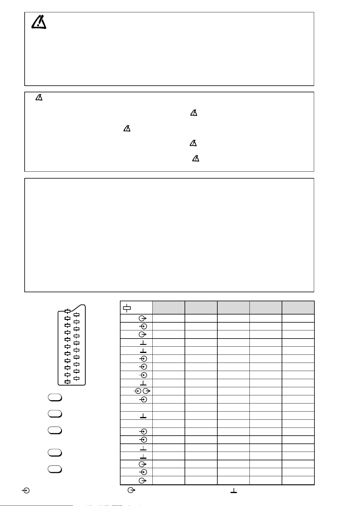
Indicates critical safety components, and identical components should be used for replacement. Only then can the
operational safety be garanteed.
Le remplacement des éléments de sécurité (repérés avec le symbole ) par des composants non homologués selon la
Norme CEI 65 entraine la non-conformité de l'appareil. Dans ce cas, la responsabilité du fabricant n'est plus engagée.
Wenn Sicherheitsteile (mit dem Symbol gekennzeichnet) nicht durch Original - Ersatzteile ersetzt werden, erlischt die
Haftung des Herstellers.
La sostituzione dei componenti di sicurezza (evidenziati con il segno ) con componenti non omologati secondo la
norma CEI 65 comporta la non conformitá dell'apparecchio. In tal caso è "esclusa la responsabilità " del costruttore.
La sustitución de elementos de seguridad (marcados con el simbolo ) por componentes no homologados segun la
norma CEI 65, provoca la no conformidad del aparato. En ese caso, el fabricante cesa de ser responsable.
MEASUREMENT CONDITIONS - CONDITIONS DE MESURES - MESSBEDINGUNGEN
CONDIZIONI DI MISURA - CONDICIONES DE MEDIDAS
RICEVITORE :
In UHF, livello d'entrata 1 mV, monoscopio barre :
- PAL, norma G. bianco 100%.
Via SCART, livello d'entrata 1 Vpp, monoscopio barre :
Colore, Contrasto, Luminositá media, Suono minimo.
Programma selezionato PR 01.
Tensioni continue rilevate rispetto alla massa con un voltmetro digitale.
RECEIVER :
On UHF,input level : 1 mV, bar test pattern :
- PAL, I standard, 100% white.
Via the scart socket, input level : 1 Vpp, bar test pattern :
Colour, contrast and brightness at mid-position, sound at minimum.
Programme selected : PR 01.
DC voltages measured between the point and earth using a digital
voltmeter.
EMPFÄNGER :
Bei UHF Eingangspegel 1 mV, Farbbalken :
- PAL, Norm G, Weiss 100%.
Über die Scartbuchse : Eingangspegel 1 Vss, Farbbalken :
Farbe, Kontrast, Helligkeit in der Mitte des Bereichs, Ton auf Minimum.
Zugeordnetes Programm PR 01.
Gleichspannungen mit einem digitalen Voltmeter zur Masse gemessen.
RECEPTEUR :
En UHF, niveau d'entrée 1 mV mire de barres
- SECAM, Norm L, Blanc 100%.
Par la prise Péritélévision, niveau d'entrée 1 Vcc, mire de barres .
Couleur, contraste, lumière à mi-course, son minimum.
Programme affecté PR 01.
Tensions continues relevées par rapport à la masse avec un
voltmètre numérique.
RECEPTOR :
En UHF, nivel de entrada 1 mV, mira de barras :
- PAL, norma G, blanco 100%.
Por la toma Peritelevision, nivel de entrada 1 Vpp mira de barra.
Color, Contraste, luz a mitad de carrera, Sonido minimo.
Programa afectado PR 01.
Tensiones continuas marcadas en relacion a la masa con un voltimetro digital.
MAIN
FRANÇAIS ESPAÑOLDEUTSCHENGLISH ITALIANO
1
2
3
4
5
6
7
8
9
10
11
12
13
14
15
16
17
18
19
20
21
NC
21
17
19
15
13
20
18
16
14
12
11
9
10
8
7
5
3
1
6
4
2
NC
AUDIO "R"
AUDIO "R"
AUDIO "L"
NOTE :
... etc. identifies each
pcb module.
AUDIO "D"
AUDIO "D"
AUDIO "G"
AUDIO
"BLEU"
AUDIO "G" MONO
"BLEU"
COMMUT. LENTE
"VERT"
"VERT"
"ROUGE"
COMMUT. RAPIDE
COMMUT. RAPIDE
VIDEO
VIDEO SYNCHRO
BLINDAGE PRISE
AUDIO "R"
AUDIO "R"
AUDIO "L"
AUDIO
"BLAU"
AUDIO "L" MONO
"BLAU"
AV
UMSCHALTUNG
"GRÜN"
"GRÜN"
"ROT"
AUSTASTUNG
AUSTASTUNG
VIDEO
VIDEO ODER
SYNCHRO
ABSCHIRMUNG
DES STECKERS
AUDIO "D"
AUDIO "D"
AUDIO "I"
AUDIO
"AZUL"
AUDIO "I" MONO
AZUL
"CONMUTACION
LENTA"
"VERDE"
"VERDE"
"ROJA"
"CONMUTACION
RAPIDA"
"CONMUTACION
RAPIDA"
VIDEO
VIDEO O SINCRO
BLINDAJE
DEL ENCHUFE
AUDIO "D"
AUDIO "D"
AUDIO "S"
AUDIO
"BLU"
AUDIO "S" MONO
BLU
"COMMUTAZIONE
LENTA"
"VERDE"
"VERDE"
"ROSSO"
"COMMUTAZIONE
RAPIDA"
"COMMUTAZIONE
RAPIDA"
VIDEO
VIDEO O SINCRO
INVOLUCRO METAL-
LICO DELLA PRESA
AUDIO "L" MONO
"BLUE"
"GREEN"
AV LINK AV LINK AV LINK AV LINK AV LINK
"GREEN"
"RED"
"ROUGE" "ROT" "ROJA""ROSSO""RED"
SLOW SWITCH
FAST SWITCH
VIDEO
VIDEO VIDEO VIDEOVIDEOVIDEO
PLUG SCREEN
BOX
VIDEO OR "SYNC"
FAST SWITCH
AUDIO
"BLUE"
: OUTPUT - SORTIE - AUSGANG - USCITA - SALIDA •
: EARTH - MASSE - MASSE - MASSA - MASA
MAIN
NOTE :
... etc. repères des
platines constituant l'appareil.
MAIN
NOTA :
... etc. marcas de las
placas que constituyen el
aparato.
MAIN
NOTA :
... ecc. sigla delle
piastre dell' apparecchio.
MAIN
HINWEIS :
... usw. Kennzeichnung
der Platinen, aus denen das
Gerät zusammengesetzt ist.
: INPUT - ENTRÉE - EINGANG - ENTRATA - ENTRADA •
Do not disconnect modules when they are energized!
Repairs on power supply section are to be carried out only with isolating transformer.
Ne pas retirer les modules lorsqu' ils sont sous tension. N'effectuer les travaux de maintenance sur la partie reliée
au secteur (Switch Mode) qu'au travers d'un transformateur d'isolement.
Module nicht bei eingeschaltetem Gerät entfernen!
Servicearbeiten am Netzteil nur unter Verwendung eines Regeltrenntrafos durchführen.
Non scollegare le piastre quando sono alimentate!
Per le riparazioni sulla sezione alimentatore, utilizzare un trasformatore isolatore.
No desconectar los módulos cuando están activados. Las reparaciones en la sección de alimentación de energía
deben ser ejecutadas solamente con un transformador de separación.
Page 3

DTH6300
First issue 03 / 05 3
SOMMAIRE
Page
CARACTERISTIQUES TECHNIQUES . . . . . . . . . . . . . . . . . . . . . . . .4
PREVENTION CONTRE LES DECHARGES ELECTRIQUE . . . . . .5 / 6
MANIPULATION DU BLOC OPTIQUE . . . . . . . . . . . . . . . . . . . . .7 / 8
SCHEMA D' INTERCONNEXION / REGLAGE . . . . . . . . . . . . . . . . .9
SCHEMA SYNOPTIQUE (VCR) . . . . . . . . . . . . . . . . . . . . . . . . . . .10
SCHEMA DES CIRCUITS D’ALIMENTATIONS . . . . . . . . . . . .11/14
SCHEMA DE LA PLATINE PRINCIPALE . . . . . . . . . . . . . . . .15 / 34
Page
SCHEMA DES CIRCUITS COMMANDES . . . . . . . . . . . . . . . .31/32*
SCHEMA SYNOPTIQUE (DVD) . . . . . . . . . . . . . . . . . . . . . . . .35 / 36
SCHEMA DE LA PLATINE PRINCIPALE . . . . . . . . . . . . . . . .37 / 44
CIRCUIT IMPRIME PLATINE ALIMANTATION . . . . . . . . . . . . . . .45
CIRCUIT IMPRIME PLATINE COMMANDES / AFFICHEUR . . . .46*
CIRCUIT IMPRIME PLATINE PRINCIPALE . . . . . . . . . . . . . . .47/52
REGLAGE MECANIQUE - DEMONTAGE / REMONTAGE . . . . .53/78
CONTENTS
Page
TECHNICAL DATA . . . . . . . . . . . . . . . . . . . . . . . . . . . . . . . . . . . . . .4
PREVENTION OF ELECTRO STATIC DISCHARGE . . . . . . . . . .5 / 6
HANLING THE OPTICAL PICKUP . . . . . . . . . . . . . . . . . . . . . . . .7 / 8
WIRING DIAGRAM / ADJUSMENTS . . . . . . . . . . . . . . . . . . . . . . . .9
SCHEMA SYNOPTIQUE (VCR) . . . . . . . . . . . . . . . . . . . . . . . . . . .10
POWER SUPPLY . . . . . . . . . . . . . . . . . . . . . . . . . . . . . . . . . . .11/14
MAIN SCHEMATIC DIAGRAM (VCR ) . . . . . . . . . . . . . . . . . .15 / 34
Page
CONTROL SCHEMATIC DIAGRAM . . . . . . . . . . . . . . . . . . . .31/32*
BLOCK DIAGRAM (DVD) . . . . . . . . . . . . . . . . . . . . . . . . . . . .35 / 34
MAIN SCHEMATIC DIAGRAM (DVD ) . . . . . . . . . . . . . . . . . .37 / 44
POWER SUPPLY P.C.B . . . . . . . . . . . . . . . . . . . . . . . . . . . . . . . . .45
KEYBOARD /DISPLAY /CLOCK . . . . . . . . . . . . . . . . . . . . . . . . . .46*
MAIN P.C.B . . . . . . . . . . . . . . . . . . . . . . . . . . . . . . . . . . . . . .47 / 52
MECHANICAL ADJUSTMENT-DISASSEMBLY/ASSEMBLY . .53/78
SUMARIO
Página
DATOS TECNICOS ............................................................................4
PREVENCIÓN CONTRA DESCARGAS ELECTRO-STATICA ........5 / 6
MANEJO DEL OPTICO .................................................................7 / 8
ESQUEMA DE INTERCONEXIONES / AJUSTES............................9
SCHEMA SYNOPTIQUE (VCR) .......................................................10
ESQUEMA DE LOS CIRCUITOS DE ALIMENTACIÓN..............11/14
ESQUEMA DE LA PLATINA PRINCIPAL ...............................15 / 34
Página
ESQUEMA DE LOS CIRCUITOS MANDOS ............................31/32*
ESQUEMA DE BLOQUES (DVD).............................................35 / 36
ESQUEMA DE LA PLATINA PRINCIPAL................................37 / 44
PLATINA ALIMANTACIÓN .............................................................45
PLATINA MANDOS / INDICADOR / RELOJ..................................46*
PLATINA PRINCIPAL.................................................................47/52
AJUSTES MECANICOS - DESMONTAR/VOLVER A MONTAR .....53/78
SOMMARIO
Pagina
DATI TECNICI . . . . . . . . . . . . . . . . . . . . . . . . . . . . . . . . . . . . . . . . . .4
AZIONI PREVENTIVE CONTRO LE SCARICHE ELETTROSTATICHE 5 /6
MANEGGIAMENTO OTTICA PICKUP . . . . . . . . . . . . . . . . . . . . . .7 / 8
DIAGRAMMA DELLE INTERCONNESSIONI /REGOLAZIONI . . . . .9
SCHEMA A BLOCCHI (VCR) . . . . . . . . . . . . . . . . . . . . . . . . . . . . . .10
ALIMENTAZIONE . . . . . . . . . . . . . . . . . . . . . . . . . . . . . . . . . . . .11/14
SCHEMA DELLA PIASTRA PRINCIPALE . . . . . . . . . . . . . . .15 / 34
Pagina
SCHEMA DEI CIRCUITI TASTIERA . . . . . . . . . . . . . . . . . . . .31/32*
SCHEMA A BLOCCHI (DVD) . . . . . . . . . . . . . . . . . . . . . . . . .35 / 36
SCHEMA DELLA PIASTRA PRINCIPALE . . . . . . . . . . . . . . .37 / 44
PIASTRA DEI CIRCUITI DI ALIMENTAZIONE . . . . . . . . . . . . . . . . .45
PIASTRA TASTIERA / INDICATORE / OROLOGIO . . . . . . . . . . . .46*
PIASTRA PRINCIPALE . . . . . . . . . . . . . . . . . . . . . . . . . . . . . . . .47/52
ISTRUZIONI PER LA MANUTENZIONE MECCANICA . . . . . . . .53/78
INHALT
Seite
TECHNISCHE DATEN . . . . . . . . . . . . . . . . . . . . . . . . . . . . . . . . . . . .4
VERMEIDUNG VON ELEKTROSTATISCHER ENTLADUNG (ESD)5 / 6
HANDHABUNG DER OPTISCHEN EINHEIT . . . . . . . . . . . . . . . .7 / 8
VERDRAHTUNGSPLAN / EINSTELLLUNGEN . . . . . . . . . . . . . . . .9
SCHEMA SYNOPTIQUE (VCR) . . . . . . . . . . . . . . . . . . . . . . . . . . .10
NETZTEIL . . . . . . . . . . . . . . . . . . . . . . . . . . . . . . . . . . . . . . . . .11/14
SCHALTBILD HAUPTPLATINE . . . . . . . . . . . . . . . . . . . . . . . .15 / 34
Seite
SCHALTBILD BEDIENTEIL/ ANZEIGE . . . . . . . . . . . . . . . . . .31/32*
BLOCKSCHALBILD (DVD) . . . . . . . . . . . . . . . . . . . . . . . . . . .35 / 36
SCHALTBILD HAUPTPLATINE . . . . . . . . . . . . . . . . . . . . . . . .37 / 44
LEITERPLATTE NETZTEIL . . . . . . . . . . . . . . . . . . . . . . . . . . . . . . .45
LEITERPLATTE BEDIENTEIL/ ANZEIGE . . . . . . . . . . . . . . . . . . .46*
GRUNDPLATTE . . . . . . . . . . . . . . . . . . . . . . . . . . . . . . . . . . . . .47/52
MECHANISCHE EINSTELLUNGEN-DEMONTAGE/MONTAGE . . .53/78
Some Models*
Page 4

DTH6300
4 First issue 03 / 05
TECHNICAL DATA - CARACTERISTIQUES TECHNIQUES TECHNISCHE DATEN - DATI TECNICI - DATOS TECNICOS
• THOMSON Multimedia reserves the right to change the specifications without notice
• Tous droits de modification des spécifications réservés.
• Änderungen der technischen Daten sind ohne Ankündigung möglich.
• Con riserva di modifica dei dati tecnici senza preavviso.
• Nos reservamos el derecho de modificar los datos técnicos sin previo aviso.
PLAYABLE DISK TYPE DVD
Video DVD+R/+RW/-R/-RW+VCD/S-VCD
audio CD audio + most of CD-R/CD-RW
MODULATOR
Video (2) jpeg
System PLL I (DTH6300F) / - (DTH6300E)
DiviX "Home cinema certified" yes
Channel range 21-69 (DTH6300F) / - (DTH6300E)
Regional code 2
Auto channel select Yes (DTH6300F) / - (DTH6300E)
Disk sizes 8 + 12 cm
AUTO MODES
VIDEO DVD
Auto power on Yes
Output signal PAL / PAL 60 Hz / NTSC
Auto playback Yes
Digital to analog converter 10 Bit / 27 MHz
Auto rewind Yes
Progressive video processor Yes (DTH6300F) / - (DTH6300E)
VIDEO VCR
TIMER
Colour System Pal / Secam (DTH6300F / Pal (DTH6300E)
Timer capacity 7 events / 1 month
MESECAM Yes
Daily / weekly repeat Mo-Fr/Yes
NTSC playback (PB) on PAL TV Yes
Power back-up EEPROM
Yes (DTH6300F) / - (DTH6300E)
Heads (Video+Audio+FEH) 4+2
PDC decoder
VPS decoder
Yes
Tape speed SP / LP / SLP (NTSC)
Easy programming ShowView (DTH6300F) / Video Plus + (DTH6300E)
Still Picture Noiseless (SP)
Slow Motion Noiseless (SP)
Frame advance Noiseless (SP)
Tracking Digital Auto
Instant recording Yes
Assemble Yes
CLOCK
16:9 identif. REC./PB Auto
System Quartz
AUDIO DVD
Clock setting Auto(TXT/UTC)
Digital to analog converter 96 kHz / 24 bits
Power back-up (min) 3 sec
Signal to Noise ratio 100 dB
DISPLAY
Dolby Digital 5.1 Passthrough
Graphical user interface Yes
DTS Passthrough
OSD langages GB,D,F,I,E,NL
MPEG 2 audio Passthrough
Front display technology LED
FRONT CONNECTORS
MP3 decoder built in Yes
RCA Audio IN 2
Virtual surround Yes
RCA video IN 1
Voice enhancing effect NA
AUDIO VCR
HIFI Stereo Yes
REAR CONNECTORS
Number of scart sockets 2
… of which Y/C 1
PLAYBACK FEATURES DVD
…of which RGB 1
Still picture Yes
Scart with RGB loop 1
Frame advance Yes
RCA video out 1
Repeat function DVD Tittle/Chapter/AB
Repeat function CD Disk / track / Program
Digital audio out Coaxial & Optical
YPrPb (component) RCA Yes
Program play Yes (CD/mp3)
REMOTE CONTROL
Random play Yes (CD/mp3)
Model Multiproduct (DTH6300F) / RCT311DA1(DTH6300E)
Dealers mode Yes
Type 3 in 1 : TH TV / TH VCR / TH DVD
Parental lock Yes
SUPPLIED ACCESSORIES
Zoom Yes
RCU battery 2 x AAA
Power cable / Plug FIXED / CEE (DTH6300F) / UK fuse (DTH6300E)
Variable search speed Yes x 4 speed/SCAN/Slow
Scart cable Yes
Resume memory 1 disc
RCA A/V cable Yes
Introscan Yes (CD)
Scene again Yes
IB languages (1) F/D/I/NL/GB (DTH6300F) / GB (DTH6300E)
jpeg photos playback Yes (Slideshow)
jpeg combination playback jpeg & mp3
GENERAL DATA
Kodak Picture CD Playback Yes
Product size (W x H x D in mm) 430 x 79 x 255
TAPE ACCESS
Packaging size (W x H x D in mm) TBD
Counter Real time
Weight : Net / Gross (Kg) 4/ 5,4
EAN code 3244480148518
Power supply 230 V - 50 Hz
Power consumption 21 W (DTH6300F) / 23W (DTH6300E)
Standby Power Consumption <3 W (DTH6300F) / 6,3W (DTH6300E)
NOTE*
Auto Power / Rewind / Eject Yes
Most CD-R / CD-RWs Total compatibility not guaranteed
Tuning system PLL
Standard LL', BG, DKK'(DTH6300F) / BG,DKK' (DTH6300E)
Programme Number 88
NICAM / FM Stereo Sound I / - (DTH6300F) // L,BG, DK/ BG, DK (DTH6300E)
Auto installation Yes
Auto sorting Yes
RECEPTION
FEATURES BENEFITS
Combines all features of a DVD player and HiFi VHS videorecorder Easy connection and upgrade to DVD in one compact unit
Built-in mp3 decoder, CD-R, CD-RW & S-VCD playback Allows playback of DVD discs, CD audio and most CD-R / CD-RW* as well as listening to
your own MP3 CDs* & S-VCD discs
DivX playback (DivX®5, DivX®4, DivX®3 and DivX®VOD) "Home Theatre Certified" Plays videos and movies downloaded from internet.
Ready for future DivX formats
VPS and PDC function Don't miss the recording if the program starts late (on VPS and PDC channels)
Showview For easy and quick recording thanks to the showview code
2 scarts with loop-through (among them 1 RGB) For an easier installation of your DVD / VCR with other Audio and Video equipment.
RGB to enhance picture quality transmitted to your TV
Front A-V connectors For easy recording from external equipment like camcorders
Page 5
6
DTH6300
First issue 03 / 05 5
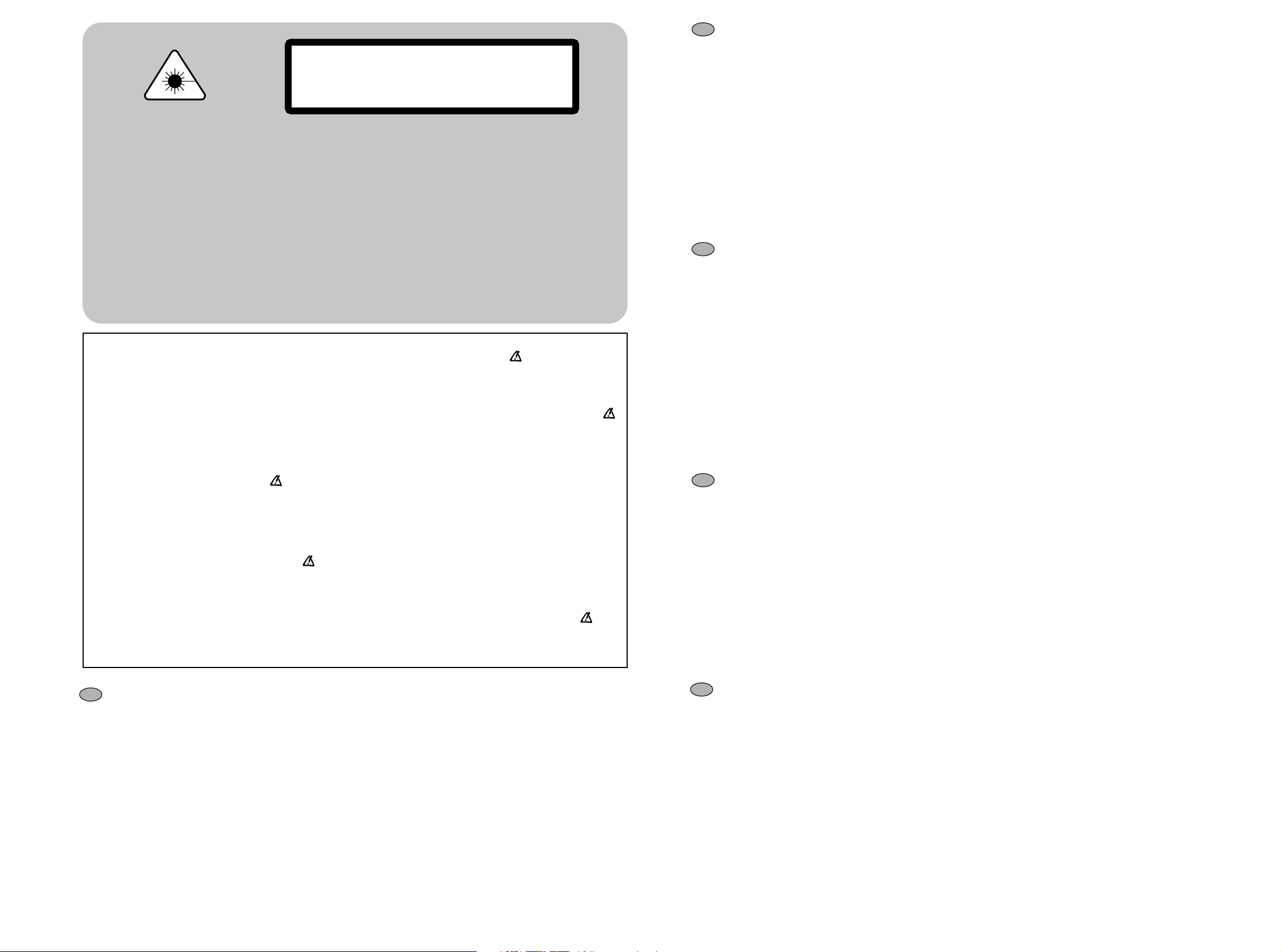
Invisible laser radiation when open and interlock
failed or defeated. Avoid direct exposure to beam.
Le rayon laser est invisible. Eviter l'exposition directe
lors de la maintenance.
Bei geöffneter Schublade und Defekt der Sicherheitsvorrichtungen besteht die Gefahr unsichtbaren
Laserlichts. Niemals direkt in den Laserstrahl sehen.
Il raggio laser è invisible. Evitare l'esposizione diretta
durante la manutenzione.
El rayo laser es invisible. Evitar la exposición directa
en el momento del mantenimiento.
DANGER :
ATTENTION :
VORSICHT BEI
REPARATUREN :
ATTENZIONE :
IMPORTANTE :
CLASS 2 LASER PRODUCT
APPAREIL A LASER DE CLASSE 2
LASER KLASSE 2
APPARECCHIO CON LASER DI CLASSE 2
APARATO CON LASER DE CLASE 2
IMPORTANT SAFETY NOTICE
There are special components used in this equipment which are imporant for safety. These part are marked by symbol on the schematic
circuit diagrams and replacement part list. It is essential that these safety critical components are replaced with the manufacture’s specified
parts to prevent electric shock, fire, or other hazards. do not attempt to modify the original design without permission of the manufacturer.
REMARQUES DE SECURITE IMPORTANTE
Il y a des composants spéciaux utilise dans cet appareil qui sont important pour la sécurité. Ces pièces sont repérées par un symbole
sur les schémas de principes et la liste de pièces détachées. Il est essentiel que ces composants de sécurité soient remplacés par les
pièces spécifiques du constructeur pour éviter les chocs électriques, feux ou autres risques. Ne tentez pas de modifier la conception
originale sans autorisation du constructeur.
WICHTIGER SICHERHEITSHINWEIS
In diesem Gerät wurden sicherheitsrelevante Komponenten verwendet. Diese Teile sind im Schaltbild und in der Ersatzteilliste mit
einem Symbol markiert. Es ist wichtig, dass diese kritischen Komponenten ausschließlich durch solche ersetzt werden, die den
Spezifikationen des Herstellers entsprechen. Die Produkthaftung des Herstellers erlischt bei Einsatz von nicht den Spezifikationen
entsprechenden Sicherheitsbauteilen und bei eigenmächtigen Schaltungsänderungen.
IMPORTANTE INFORMAZIONE DI SICUREZZA
Ci sono speciali componenti usati in questa apparecchiatura che sono importanti per la sicurezza. queste parti sono facilmente identificabili,
sullo schema e sulla lista parti, da un apposito simbolo . E’ indispensabile che questi componenti di sicurezza, nel caso di alterazioni o
guasti, vengano sostituiti con specifici ricambi originali per evitare shock elettrici, fuoco o altri rischi. Non modificare mai il circuito senza
autorizzazione della casa costruttrice.
AVISO IMPORTANTE SOBRE SEGURIDAD
En este equipo se utilizan componentes especiales que son muy importantes para la seguridad. están marcados con el símbolo en los
esquemas eléctricos y en las listas de repuestos. Es fundamental que estos componentes críticos de seguridad, sean reemplazados por las
piezas originales indicadas por el fabricante para evitar los peligros de electrocución, de fuego, etc. y no modificar el diseño original sin
autorización del fabricante.
EN Prevention of electro static discharge (esd) to Electrostatically Sensitive Devices (ESD)
Some semiconductor devices can be damaged easily by static electricity (integrated circuits, some field-effect transistors and
semiconductor chip components. The following techniques should be used to help reduce the incidence of component damage caused
by static electricity.
1. Immediately before handling any semiconductor component or semiconductor-equipped assembly, drain off any electrostatic charge
on your body by touching a known earth ground or wear a discharging wrist strap device, which should be removed for potential
shock reasons prior to applying power to the unit under test.
2. After removing an electrical assembly equipped with ESD devices, place the assembly on a conductive surface such as aluminum
foil.
3. Use only a grounded-tip soldering iron to solder or unsolder ESD devices.
4. Use only an anti-static solder removal devices.
5. Do not use freon-propelled chemicals.
6. Do not remove a replacement ESD device from its protective package until immediately before your are ready to install it.
7. Immediately before removing the protective materials from the leads of a replacement ESD device, touch the protective material to
the chassis or circuit assembly into which the device will be installed.
CAUTION : Be sure no power is applied to the chassis or circuit, and observe all other safety precautions.
8. Minimize bodily motions when handling unpackaged replacement ESD devices
FR Prévention des composants et sous-ensembles contre les ESD ( Décharge d'Electricité Statique )
Certains semi-conducteurs peuvent être facilement endommagés par l’électricité statique (les circuits intégrés et certains transistors à
effet de champs, les composants semi-conducteurs de type chip ainsi que les diodes à émission laser équipant les lecteurs optiques ).
Les précautions suivantes doivent être utilisées pour réduire l’incidence des dommages causés par l’électricité statique.
1. Immédiatement avant de manipuler tout composant semi-conducteur ou ensemble équipé de semi-conducteurs, éliminez toute charge
électrostatique de votre corps en touchant une terre connue. Ou bien, mettez un bracelet antistatique, qui doit être retiré, pour des
raisons de choc électrique, avant de mettre l’appareil sous tension.
2. Après démontage d’un ensemble électrique équipé d’éléments sensibles aux ESD, Placez l’ensemble sur une surface conductrice telle
qu’une feuille d’aluminium.
3. N’utilisez qu’un fer à souder relier à la masse pour souder ou dessouder ces composants.
4. Pour dessouder, n’utilisez que du matériel antistatique
5. N’utilisez pas de produits chimiques à propulsion de fréon.
6. Ne retirez pas ces composants de leur emballage de protection jusqu’à ce que vous soyez prêt à l’installer.
7. Juste avant de retirer la protection des broches de ces composants, touchez la protection sur le châssis ou le circuit dans lequel le
composant va être installé.
ATTENTION : Assurez-vous que le châssis ou le circuit n’est pas sous tension, et observez toutes les autres précautions de sécurité.
8. Minimisez les déplacements corporels lorsque vous manipulez un de ces composants de remplacement déballé.
DE Vermeidung von Elektrostatischer Entladung (ESD)
Manche elektronische Komponenten wie Transistoren, Integrierte Schaltkreise oder Chipelemente können leicht durch ESD beschädigt
oder zerstört werden. Die folgenden Richtlinien helfen Schäden durch ESD zu vermeiden.
1. Unmittelbar vor dem Hantieren Halbleitern oder Baugruppen mit Halbleitern leiten Sie die statische Aufladung Ihres Körpers durch
Berühren einen geerdeten Gegenstandes ab. Beschaffen Sie sich ein leitendes Hansgelenkband. Dieses müssen Sie allerdings vor dem
Einschalten des zu prüfenden Gerätes ablegen.
2. Nach dem Ausbau einer empfindlichen elektronischen Baugruppe legen Sie diese auf einen leitende Unterlage wie Aluminium-Folie um
eine elektrostatische Entladung zu vermeiden.
3. Benutzen Sie für Lotarbeiten an empfindlichen Komponenten einen geerdeten Lötkolben.
4. Benutzen Sie antistatisches Entlötwergzeug.
5. Verwenden Sie keine Sprays, die Freon als Treibmittel enthalten. Diese können ausreichend elektrostatische Ladung erzeugen, um
empfindliche Komponenten zu schädigen.
6.
Entfernen Sie die Antistatik-Schutzverpackung (Alu-Folie, Leitgummi, Leitfolie, ..) von Komponenten und Baugruppen erst wenn Sie diese benötigen.
7. Unmittelbar vor dem Entfernen der Schutzverpackung führen Sie ein Potentialausgleich durch Berühren des Gerätes mit der
Komponente/Baugruppe durch. ACHTUNG: Stellen Sie Sicher, Dass das Gerät nicht unter Spannung steht und beachten Sie alle
einschlägigen Sicherheitsvorschriften.
8. Bewegen Sie sich beim Hantieren mit empfindlichen Komponenten/Bausteinen möglichst wenig, da die Reibung Ihrer Kleidung oder
der Füße auf dem Bodenbelag elektrostatische Ladung erzeugen kann.
IT
Azioni preventive contro le scariche elettrostatiche (esd) sui Dispositivi Sensibili Elettrostaticamente (ESD)
Alcuni semiconduttoripossono essere facilmente danneggiati da elettricità statica (circuiti integrati, alcuni transistor ad effetto di campo e
componenti chip semiconduttori). Al fine di ridurre l’incidenza dei componenti danneggiati a causa di elettricità statica si dovrebbero
osservare le seguenti precauzioni.
1.
Immediatamente prima di maneggiare qualsiasi tipo di componente semiconduttore o di apparecchio che impiega semiconduttori, scaricare le
possibili cariche elettrostatiche del proprio corpo toccando un punto sicuramente collegato a terra. In alternativa, indossare un apposito braccialetto
antistatico che dovrebbe però essere tolto, per possibili potenziali shock, immediatamente prima di alimentare l’apparecchiatura sotto test.
2. Dopo il disimballo porre l’apparecchiatura equipaggiata con dispositivi ESD su una superficie conduttiva tipo foglio di alluminio.
3. Usare saldatori con punta a massa per saldare o dissaldare dispositivi ESD.
4. Usare solo saldatorI antistatici.
5. Non usare prodotti chimici tipo freon.
6. Rimuovere il dispositivo ESD dal suo imballo protettivo solo immediatamente prima del suo utilizzo.
7. Immediatamente prima della rimozione del materiale protettivo dai piedini del dispositivo ESD di ricambio, toccare con il materiale
protettivo il telaio o la massa del circuito stampato dove il dispositivo deve essere inserito.
ATTENZIONE : Assicurarsi che il circuito o il telaio non sia alimentato, e osservare tutte le altre precauzioni di sicurezza.
8. Limitare gli spostamenti quando si maneggia un dispositivo ESD disimballato.
ES Prevención contra descargas electro-státicas (esd) para los DISPOSITIVOS SENSIBLES electrostáticamente (ESD)
Algunos dispositivos semiconductores, pueden ser dañados fácilmente por la electricidad estática (los circuitos integrados, algunos
transistores de Efecto de Campo y los semiconductores "chip"). Las siguientes técnicas pueden ser utilizadas para ayudar a reducir la
destrucción de los componentes causada por la electricidad estática.
1. Inmediatamente antes de manejar cualquier componente semiconductor o conjunto equipado con semiconductores, elimine la carga
electrostática de su cuerpo tocando alguna toma de tierra conocida o utilizar una correa conductora conectada a una toma de tierra que
se pone en la muñeca la cual debe ser quitada (por razones de seguridad) antes de conectar la alimentación al equipo bajo prueba.
2. Después de quitar un conjunto equipado con componentes ESD, coloque el conjunto sobre una superficie conductora, como papel aluminio.
3. Utilizar únicamente soldadores con la punta conectada a la toma de tierra para soldar o desoldar componentes ESD.
4. Utilizar solamente soldadores antiestáticos para quitar componentes.
5. No utilizar productos químicos con gas freón como propelente.
6. No sacar de su embalaje protector el nuevo componente ESD hasta inmediatamente antes de estar todo preparado para montarlo.
7. Inmediatamente antes de quitar los materiales de protección de las patillas del componente, tocar el material protector al chasis del
conjunto donde se vaya a montar el componente.
CUIDADO : Asegúrese de que la alimentación no esté aplicada al chasis o circuito, y cumpla todas las precauciones de seguridad.
8. Maneje sin movimientos bruscos el componente ESD una vez desempaquetado.
Page 6
7
DTH6300
8 First issue 03 / 05
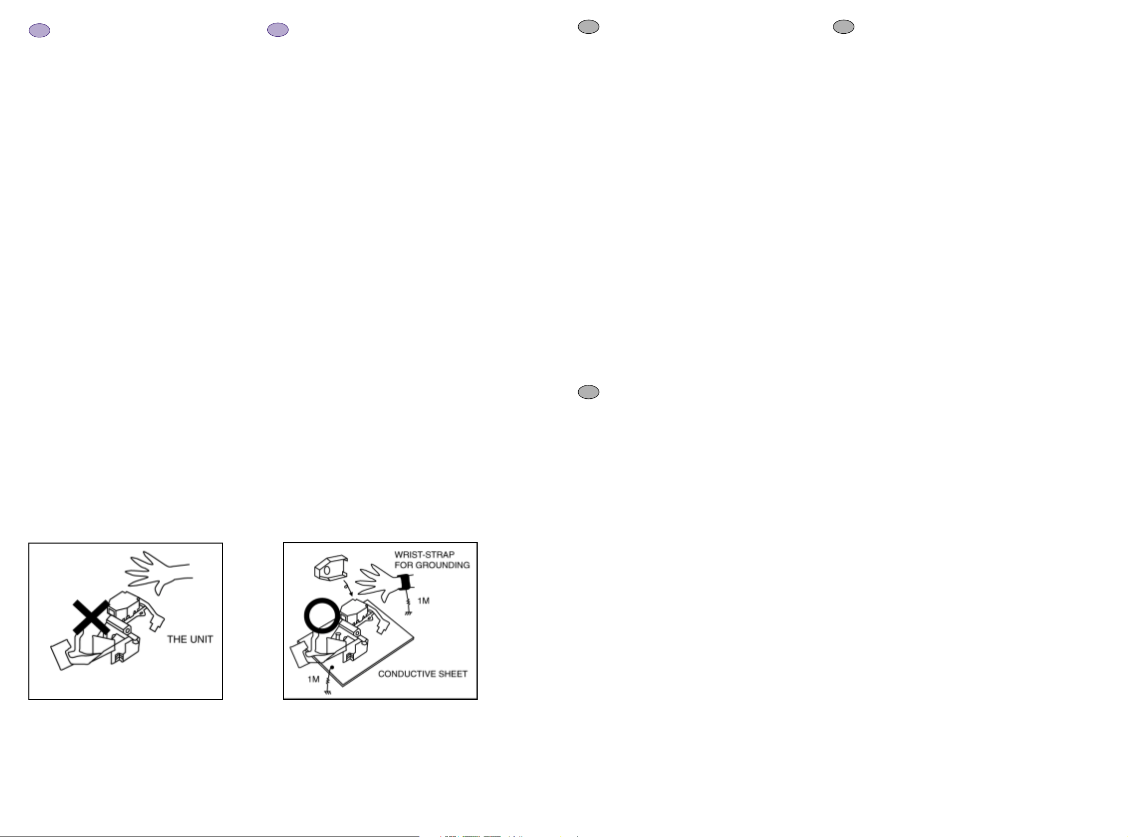
HANDLING THE OPTICAL PICKUP
The laser diode used in the optical pickup may break down
due to potential differences caused by electricity produced
by clothing or the human body, care should therefore be
taken to prevent electrostatic discharge whilst repairing the
optical pickup.
The following method is recommended.
1) Place a conductive sheet on the work bench (The black
sheet used for wrapping repair parts.)
2) Place the set on the conductive sheet so that the
chassis is grounded to the sheet.
3) Place your hands on the conductive sheet (doing this
gives them the same ground as the sheet.
4) Remove the optical pickup block
5) Perform work on top of the conductive sheet. Be careful
not to let your clothes or any other static sources to
touch the unit.
* Grounding the Human Body, use an antistatic wrist
strap to discharge static electricity from your body.
* Grounding the work place, use either an antistatic matt
or a sheet of steel on the area where the optical pickup
is to be placed and ground the matt/sheet.
6) Short the short terminal on the PCB, which is inside the
Pickup Assembly, before deconnecting the flexible
cable for replacing the Pickup. (The short terminal is
shorted when the Pickup Assembly is being lifted or
moved.)
7) After replacing the Pickup, open the short terminal on
the PCB.
MANIPULATION DU BLOC OPTIQUE
La diode laser utilisée dans le bloc optique peut se
détériorer à cause d’une différence de potentiel causé par
l’électricité produite par les vêtements ou le corps humain,
par conséquent des précautions doivent être prise pour
éviter les décharges électrostatiques pendant la réparation
du bloc optique.
Il est recommandé de suivre la méthode suivante.
1) Placez une feuille conductrice sur le banc de travail (la
feuille noire utilisée pour envelopper les pièces
détachées).
2) Placez l’ensemble sur la feuille conductrice pour que le
châssis soit mis à la masse par la feuille.
3) Mettez vos mains sur la feuille conductrice (en faisant
ceci, vous leur donnez la même masse que la feuille)
4) Retirez le bloc optique
5) Travaillez en haut de la feuille conductrice. Prenez soin
de ne pas laisser vos vêtements ou autre source
statique toucher le bloc optique.
* Mise à la terre du corps humain : utilisez un bracelet
antistatique pour décharger l’électricité statique de
votre corps.
* Mise à la terre du poste de travail : placez soit un tapis
antistatique, soit
une feuille d’acier sur le banc de travail où vous
poserez le bloc optique après avoir relier le tapis ou la
feuille à la masse.
6) Pour remplacer le bloc optique, soudez le court-circuit
sur le circuit imprimé qui se trouve sur l’ensemble
optique, avant de déconnecter le câble flexible (le
court-circuit est soudé lorsque l’ensemble optique est
levé ou déplacé).
7) Après le remplacement du bloc optique, dessoudez le
court-circuit sur le circuit imprimé.
EN
FR
Fig. 1
Fig. 2
DE IT
ES
HANDHABUNG DER OPTISCHEN EINHEIT
Die verwendete Laser-Diode kann unter Umständen zerstört
werden, wenn sie mit statischer Spannung aufgeladene Teile in
Berührung kommt . Deshalb ist unbedingt zu beachten, daß vor
der Reparatur alle Teile potentialfrei sind.
Empfehlenswert ist folgende Methode.
1) Eine leitende Unterlage auf den Werktisch legen (über
1MOhm Widerstand geerdete Leitgummi-Matte, Metallplatte
oder ggf. die schwarze Folie der Ersatzteilverpackung).
2) Das Gerät auf diese Fläche stellen, damit ein
Potenzialausgleich stattfinden kann.
3) Bringen Sie Ihren Körper auf das gleiche Potenzial wie die
Unterlage (z.B. mit Handgelenkband über 1 MOhm
geerdet).
4) Jetzt kann das DVD-Laufwerk bzw. die optische Einheit
ausgebaut werden .
5) Führen sie alle Arbeiten auf der Leitgummi-Matte aus.
6) Zum Schutz des Lasers verbinden vor dem Ausbau der
optischen Einheit (Lösen der Flachbandleitung) die beiden
Lötpunkte auf der Leiterplatte der optischen Einheit
miteinander. Die Leiterplatte befindet sich in der optischen
Einheit.
7) Nach dem Einbau der (neuen) optischen Einheit den
Kurzschluß wieder beseitigen !
MANEGGIAMENTO OTTICA PICKUP
Il diodo laser usato nelle ottiche pickup si può danneggiare a
causa di differenze di potenziale causate da elettricità prodotta
da vestiti o dal corpo umano, particolari attenzioni devono
essere prese, durante la riparazione di apparecchiature con
pickup ottici, per prevenire scariche elettrostatiche.
Si raccomanda di seguire le seguenti indicazioni.
1) Mettere un foglio conduttivo sul banco di lavoro (tipo foglio
nero utilizzato per avvolgere le parti di ricambio).
2) Posizionare l’apparecchiatura sul foglio conduttivo per
collegare la massa del telaio al foglio conduttivo.
3) Toccare con le mani il foglio conduttivo per avere lo stesso
potenziale di massa del foglio conduttivo.
4) Rimuovere l’assieme ottica pickup.
5) Lavorare sopra il foglio conduttivo. Evitare di far toccare i
propri vestiti o qualsiasi altra sorgente statica
all’apparecchiatura.
* Per scaricare a massa l’elettricità statica del proprio corpo
utilizzare l’apposito braccialetto antistatico.
* Per mettere a terra il proprio posto di lavoro utilizzare un
tappetino antistatico o un foglio di acciaio collegati a massa,
sull’area dove deve essere sostituita l’ottica.
6) In caso di sostituzione del pick up, cortocircuitare prima gli
appositi punti della piastrina dell’assieme pickup, poi
scollegare il cavo di collegamento flessibile.
7) Aprire il cortocircuito dei terminali solo dopo la sostituzione
del Pickup.
MANEJO DEL CONJUNTO OPTICO
El diodo láser utilizado en el lector óptico puede resultar
averiado a causa de las diferencias de potencial eléctrico
producidas por el roce con la ropa o con el cuerpo humano,
también hay que tener cuidado de que no se produzcan
descargas electrostáticas mientras se repara el lector óptico.
Se recomienda el siguiente método.
1) Colocar una hoja conductora en el banco de trabajo (Vale la
hoja negra que se utiliza para envolver los repuestos).
2) Colocar el aparato en la hoja conductora de forma que el
chasis haga contacto con la hoja.
3) Poner las manos sobre la hoja conductora (haciendo esto
se da la misma toma de tierra que a la hoja).
4) Retirar el conjunto óptico.
5) Realice el trabajo encima de la hoja conductora. Tenga
cuidado para no permitir que su ropa o cualquier otra fuente
de electricidad estática pueda tocar a la unidad.
* Conecte a tierra el cuerpo humano, utilizando una
muñequera antiestática para descargar la electricidad
estática del cuerpo.
* Conectar a tierra el lugar de trabajo, utilizando una
alfombrilla antiestática o una hoja de papel de aluminio en
el área donde
se coloque el lector óptico y conectándola a la toma de
tierra.
6) Poner en cortocircuito los terminales de los diodos
(soldaduras en la cinta del conjunto óptico) antes de
desconectar el cable flexible para remplazar el lector óptico.
7) Después de cambiar el lector óptico, quitar los
cortocircuitos anteriores.
Page 7
DTH6300
First issue 03 / 05 9
ELECTRICAL ADJUSTMENTS - REGLAGES ELECTRIQUES
ELEKTRISCHE EINSTELLUNGEN - REGOLAZIONI ELETTRICHE
AJUSTES ELECTRICOS
WIRING DIAGRAM - SCHEMA D’INTERCONNEXIONS - VERDRAHTUNGSPLAN
DIAGRAMMA DELLE INTERCONNESSIONI - ESQUEMA DE INTERCONEXIONES
OVERALL WIRING DIAGRAM
DECK MDSMPS
BOARD
123456789
CF G
I-limit
5.2VA
PMC0 1
12VA(CAP)
CAP REV’H’
123456789
GND
MOT OR GND
CAP CT L
12VA(DRUM)
101112
LD IN
DFG/FG
101112
12345
6
1
2
GND
A.PB
A/E(-)
A/E(+)
CTL(-)
A.REC
P3D0 2
CTL(+ )
DRUM CT L
12345
P3D0 3
FUL L ERASE
6
1
2
123456789
24VA(28V A)
12PIN PPM0 1
123456789
101112
4VA
GND
GND
GND
14VA
33VA
5.3VA
101112
123456789
PMD01
RF_OUT
HFM_VCC
FROM P/UP
123456789
LD_DVD
MD_DVD
10111213141516171819202122
F
E
A
VCC
VREF
VR_DVD
GND_PD
10111213141516171819202122
B
D
C
FOCUS+
TRACKING-
MAIN PCB
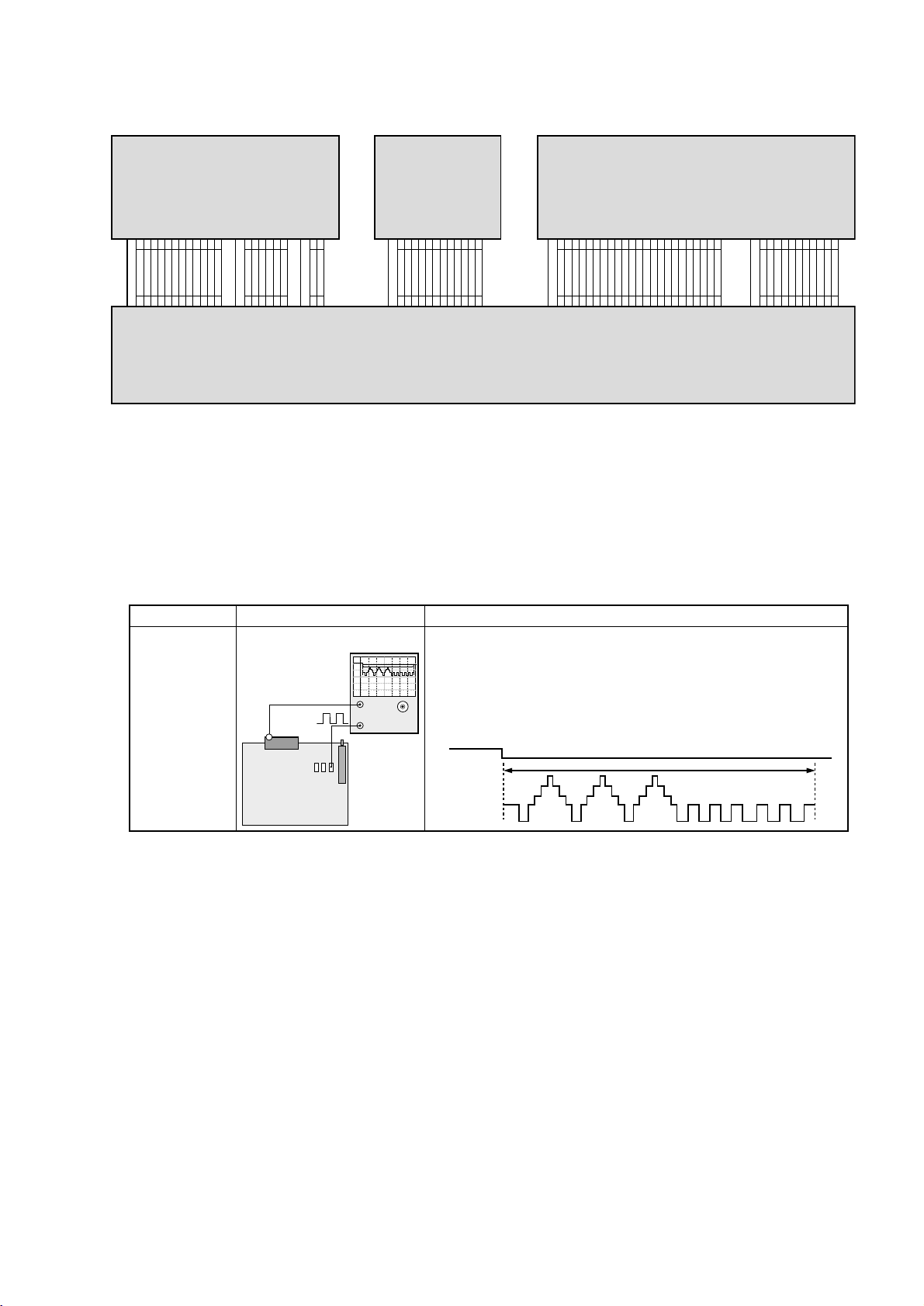
Head switching point
Mode & Signal Test Point Description
• Adjustment Procedure
a) Insert the SP Test Tape and play.
6.5H(416us)
Note - Adjust the distance of X, ( See deck mechanism adjustment page 69 )
b) Connect the CH1 of the oscilloscope to the H/SW(TP) and CH2 to the Video Out for the VCR.
c) Trigger the mixed Combo Video Signal of CH2 to the CH1 H/SW(TP), and then check
the distance (time difference), which is from the selected A(B) Head point of the H/SW(TP)
signal to the starting point of the vertical synchronized signal, to 6.5H ± 0.5H (412µs, 1H=63µs).
PB (SP)
Dual trace
Oscilloscope
SCART PIN19
Video
H/SW
Composite
VIDEO
CH1
CH2
FOCUS-
SW_PDI C
TRACKING+
LD_C D
GND_LD
MD_CD
23
VR_CD
23
123456789
SPM -
SPM +
PMD02
FROM MD
123456789
11
10
LM -
FM -
GNDSWGND
LM +
FM +
OPEN
CLOSE
11
10
VCR PCB
H/SW
H/SW
Composite
VIDEO
6.5H(416us)
• PG Adjustment Method
a-1) Payback the SP standard tape
b-2) Press the “1” key on the Remote controller and the “PLAY” key on the Front Panel the same time, then
it goes in to Tracking initial mode.
c-3) Repeat the above step(No.b-2), then it finishes the PG adjusting automatically. "off" then "on" is displayed
d-4) Stop the playback, then it goes out to PG adjusting mode after memory the PG data.
Page 8

DTH6300
10 First issue 03 / ,05
2fsc
R524, R514, R518,
R516, R589, C577,
C576, L501, Q504
LD(+)
LD(-)
L/M CONTROL
R525, R526
IC501
HD6432197A
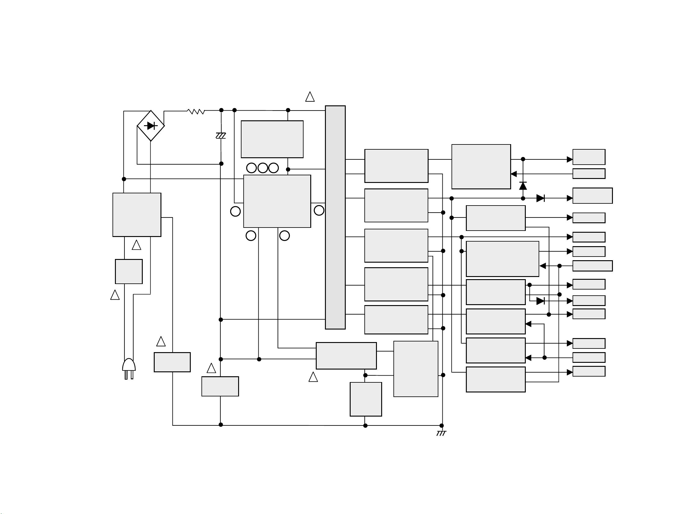
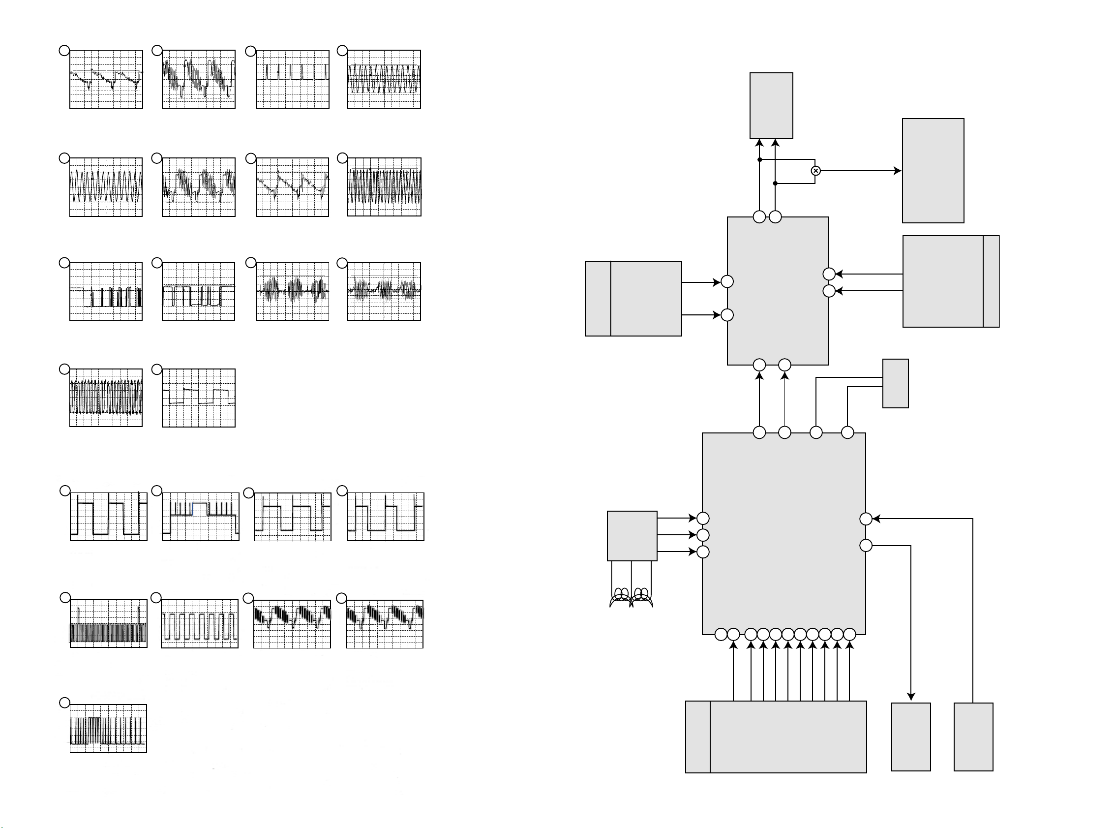
BLOCK DIAGRAM - SCHEMA SYNOPTIQUE - BLOCKSCHALTBILD - SCHEMA A BLOCCHI ESQUEMA DE BLOQUES
Page 9
12
DTH6300
First issue 03 / 05 11
BLOCK DIAGRAMS
POWER(SMPS) BLOCK DIAGRAMS
BD101
T101
TRANS
R101
+
BR BL
(BK)(WH)
C103
!
FUSE
(F101)
NOISE FILTER
BLOCK
(C101,L102,
C102)
PHOTO COUPLER
(IC102)
ERROR
AMP
(IC103)
SNUBBER
BLOCK
(D101,C105
C106,R104)
DRIVE & S/W BLOCK
(IC101, D102, R105,
C104, C109 , C135)
Y-CAP
C111
Y-CAP
C110
FEED-BACK
BLOCK
R112,R113,
C133,R114.
R115.R116
R117)
< HSR OPTION>
24V S/W BLOCK
(Q153,R151,R152,
D122,Q154,R110,
D116,R181,R182)
< HSR OPTION>
RECTIFIER&
SMOOTING BLOCK
(D106,C117,R130)
RECTIFIER&
SMOOTING BLOCK
(D110,C123,C163,
R133,L122,C126)
RECTIFIER&
SMOOTING BLOCK
(D118,D112,C129,
C131,L124,L125)
RECTIFIER&
SMOOTING BLOCK
(D111,C127,L123,
C128)
RECTIFIER&
SMOOTING BLOCK
(D113,C132,R119)
CAP VCC
13VA/24V
HSR’H ’
D117
D115
DRUM VCC
13VA
12VT
8V
5.3VA
5.0V
3.3V
D111
2.5V
33VT
TIMER’H ’
12V REG BLOCK
(Q156,ZD103,C151,
R150,R153,C152)
8V REG BLOCK
(D114,IC151,R170,
C154)
5V S/W BLOCK
(Q150,C155,D121,
R157,R158,R159,R160
Q162,R164,R172,C161)
3.3V REG BLOCK
(IC152,C153,R156)
33VT S/W BLOCK
(Q161,R154,R155
Q173,R174,R177)
5VT S/W BLOCK
(Q163,C162,R173,
R176,R175,Q164)
PWR CTL’H'
5.0VT
!
!
!
!
!
6578
2
31
BLOCK DIAGRAM - SCHEMA SYNOPTIQUE - BLOCKSCHALTBILD - SCHEMA A BLOCCHI - ESQUEMA DE BLOQUES
( SMPS )
Page 10
13
DTH6300
14 First issue 03 / 05
POWER SUPPLY - ALIMENTATION - NETZTEIL - ALIMENTAZIONE - ALIMENTACIÓN
SCHEMATIC DIAGRAM - SCHEMA DE PRINCIPE - SCHALTBILD - SCHEMA - ESQUEMA
POWE
315
(315)
T=20uS
600Vpp-H
0V
100V
(351,5)
352
5,3
(5,3)
28
(26)
14
(13)
5,3
(5,3)
14,2
(13)
Note :
Power Supply primary circuit measurements.
- Use only ( ) connection point.
Achtung :
Bei Messungen im Primärnetzteil
- Primärnetzteilmasse verwenden ( ).
Cuidado :
Medida en el bloque de alimentacion
- Utilizar la masa del bloque de alimentacion ( ).
* According to Models
315
(315)
0,8
(0,5)
Attention :
Mesure dans la partie primaire de l'alimentation
- Utiliser la masse du bloc alimentation ( ).
Attenzione :
misure nell'alimentatore primario
- usare massa alimentazione primario ( ).
Part of board connected to mains supply.
Partie du châssis reliée au secteur.
Primärseite des Netzteils.
Parte dello châssis collegata alla rete.
Parte del chassis conectar a la red.
*
3,9
(4,2)
33,9
(30)
5
(5)
4
(4)
(30) = Standby
Safety Part
When repairing, use original part only
Pièce de securité
N'utilisez que les pièces d'origine
Sicherheitsbauteil
Bei Ersatz nur Originalteil verwenden
Componenti di sicurezza
Per la riparazione utilizzare solo componenti originali
Utilice solo piezas originales
Pieza de seguridad
Use isolating mains transformer.
Utiliser un transformateur isolateur du secteur.
Einen Trenntrafo verwenden.
Utilizar un transformador aislador de red.
Utilizzare un transformatore per isolarvi dalla rete.
Page 11

16
DTH6300
First issue 03 / 05 15
POWER SUPPLY - ALIMENTATION - NETZTEIL - ALIMENTAZIONE - ALIMENTACIÓN
SCHEMATIC DIAGRAM - SCHEMA DE PRINCIPE - SCHALTBILD - SCHEMA - ESQUEMA
POWER(SMPS) CIRCUIT DIAGRAM 2
MAIN
13,4
28,3
28
33,9 33,7
33,1
13,9
5,3
4,4
13,4
11,9
12,3
5,2
5,3
4,4
5
Page 12
17
DTH6300
18 First issue 03 / 05
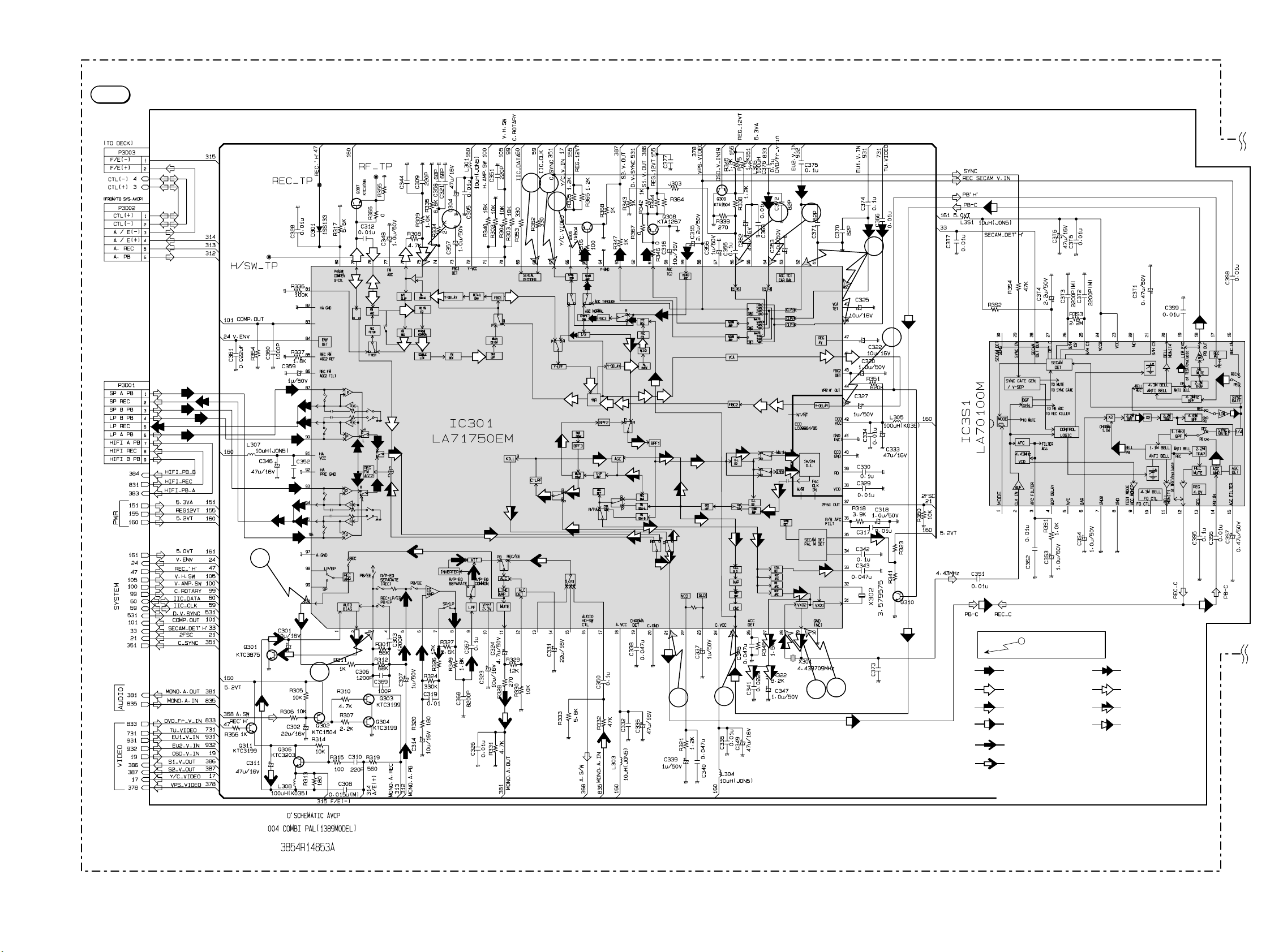
MAIN SCHEMATIC DIAGRAM - SCHEMA DE LA PLATINE PRINCIPALE - SCHALTBILD HAUPTPLATINE - SCHEMA DELLA PIASTRA PRINCIPALE- ESQUEMA DE LA PLATINA PRINCIPAL
SYSTEM CIRCUIT DIAGRAM
MAIN
5
5
1
2
9
3
6
4
8
7
WAVEFORM
Page 13
20
DTH6300
First issue 03 / 05 19
Y/C BLOCK DIAGRAM
MEASUREMENTS - MESURES - MESSUNGEN - MISURE ELABORAZIONE - MEDIDAS - TRATAMIENTO
(PB MODE)
84V.ENV
87
90
93
96
(REC MODE)
88
(To Drum )
(To Drum )
LP REC
SP REC
89
94
95
V.H.SW
C.ROT AR Y
D ATA
CLOCK
C.SYNC
79 78
PB FM
AGC
PB FM EQ FM OEM
IC301
LA71750M
REC’H’
80
79 78 76 75 70 69 68 67 65 59 58 54 52
W/D
CLIP
W/D
CLIP
REC
FM EQ
IC301
LA71750M
Killer C-LP F ACC
70
ACCC LP F
NL
EMPHA
DET AI L
ENH
V.H.SW
69 68 67
SUB LP F
MAI N
CONV
C.ROT AR Y
D ATA
CLOCK
C SYNC
Y-LP F FBC
YNR
Main
Conv
MAI N
DE EMP
Y-LP F
YNR
V.OUT
BPF
BPF
ACC
DET
MICOM
AGC
Main
Conv
65 63 61
60dB AMP
Y/C MI X
KILL DEC
REC APC
V.OUT
1H/2H
DEL AY
COMP
AMP
2721
(MICOM)
S2 V.OUT
C-Delay
(1H/2H )
CCD
LP F
CNC
2521
V.IN4
FRONT
V.IN3
DEC
SW
Y-DEL AY
VX0 2 VX0 2
2928
4.43MHz
S1 V.OUT
Y-Delay
50 V.IN2 S1
48
46
43
33
32
31
46
43
V.IN1 TUNER
CLK-IN
SYNC IN
29
IC201
LA70100M
18 14
29 16
IC201 LA70100M
212
EEPIN PB REC EEPIN PB REC
Q301
BASE 0.01 V 0.013 V 0.79 V
EMITER 0.003 V 0.004 V 0.005 V
COLECTOR
4.83 V 4.82 V 1.02 V
Q302
BASE 4.85 V 4.18 V 4.75 V
EMITER 0.002 V 4.85 V 4.75 V
COLECTOR
(-)2.79 V 4.8 V (-)25.5 V
Q303
BASE (-)2.76 V 0.7 V (-)25.6 V
EMITER (-)0.8 V 0.007 V (-)19.13 V
COLECTOR
0.002 V 0.012 V 0.004 V
Q304
BASE (-)2.62 V 0.72 V (-)25.4 V
EMITER 0.002 V 0.002 V (-)19.4 V
COLECTOR
0.002 V 0.004 V 0.004 V
Q305
BASE 1.71 V 1.41 V 1.7 V
EMITER 2.41 V 2.1 V 2.39 V
COLECTOR
0.003 V 0.004 V 0.005 V
Q309
BASE 2.18 V 2.01 V 2.33 V
EMITER 2.87 V 2.7V 3V
COLECTOR
0.012 V 0.005 V 0.012 V
Q501
BASE 0.69 V 0.69 V 0.69 V
EMITER 0.002 V 0.003 V 0.003 V
COLECTOR
0.02 V 0.012 V 0.023 V
Q502
BASE 0.31 V 0.38 V 0.33 V
EMITER 0.004 V 0.004 V 0.004 V
COLECTOR
2.65 V 1.93 V 2.4 V
Q504
BASE 0.59 V 0.51 V 0.50 V
EMITER 0.03 V 0.03 V 0.03 V
COLECTOR
3.78 V 3.75 V 3.71 V
Q5S1
BASE 0.006 V 0.005 V 0.003 V
EMITER 1.77 V 1.8 V 1.89 V
COLECTOR
2.41 V 2.1 V 2.4 V
Q515
BASE 4.94 V 0.5~4.3 V 0.4~4.9 V
EMITER 0.002 V 0.003 V 0.005 V
COLECTOR
0.02 V 0.2~3.5 V 0.4~4.9 V
Q514
BASE 4.96 V 0.8~4.2 V 0.2~4.3 V
EMITER 0.002 V 0.002 V 0.003 V
COLECTOR
0.02 V 0.01~4.8V 0.011 V
Q7S1
BASE 0.007 V 0.007 V 0.008 V
EMITER 0.001 V 0.001 V 0.001 V
COLECTOR
3.7
3.5 V0.057
V
Q801
BASE 0.7 V (-)0.1 V 0.01 V
EMITER 0.001 V 0.003 V 0.001 V
0.004V 0.006 V
Q802
BASE 0.7 V (-)0.12 V 0.7 V
EMITER 0.001 V 0.001 V 0.001 V
COLECTOR
0.004 V0.02 V0.005
Q804
BASE 1.81 V 2.5 V 1.79 V
EMITER 2.5 V 3.20V 2.48 V
COLECTOR
0.002V 0V0V
Q901
BASE 0.005 V 0.005 V 0.006 V
EMITER 0.003 V 2.04 V 1.9 V
COLECTOR
0.003 V 0.004 V 0.005 V
Q902
BASE (-)1.64 V (-)1.69 V (-)1.79 V
EMITER 0.003 V 0.004 V 0.004 V
COLECTOR
0.004 V 0.004 V 0.005 V
Q903
BASE (-)1.74 V (-)1.63 V (-)1.8 V
EMITER 0.003 V 0.003 V 0.005 V
COLECTOR
0.003 V 0.004 V 0.005 V
V
~
V
Page 14
21
DTH6300
22 First issue 03 / 05
V. HS W
( IC501 Pin 105)
1V/10ms
REC/PB MODE
1
DV.SYNC
( IC501 Pin 109)
1V/100µs
QUE/REV MODE
2
CTL(+)
( IC501 Pin 3)
1V/10ms
3
CTL(-)
( IC501 Pin 4)
1V/10ms
4
DPG/DFG
( IC501 Pin 103,104)
1V/10ms
REC/PB MODE
5
CFG
( IC501 Pin 9)
1V/10ms
6
V. IN
( IC501 Pin 17)
500mv/20µs
7
V. OU T
( IC501 Pin 19)
500mv/20µs
EE/PB MODE
8
C.SYNC
( IC501 Pin 111)
1V/100µs
EE/PB MODE
9
MEASUREMENTS - MESURES - MESSUNGEN - MISURE ELABORAZIONE - MEDIDAS - TRATAMIENTO
( VCR )
BLOCK DIAGRAM - SCHEMA SYNOPTIQUE - BLOCKSCHALTBILD - SCHEMA A BLOCCHI ESQUEMA DE BLOQUES
1
2
3
4
Hi-Fi BLOCK DIAGRAM
( IC301 Pin 75 )
PB mode PB / REC mode REC mode
500mv PP
5
( IC301 Pin 3)
REC mode PB mode PB mode
2,0 V pp
9
( IC301 Pin 68 )
PB / REC mode REC mode PB mode
5,0 V pp
13
( IC301 Pins 48, 50, 52
54, 56 )
Video in 1,0V pp
6
( IC301 Pin 65 )
PB mode
2,02 V ppp
10
( IC301 Pin 69 )
PB / REC mode
5,0 V pp
14
( IC301 Pin 67)
4,0 V pp
7
( IC301 Pin 43 )
400m V pp
11
( IC301 Pin 21 )
340m V pp
( IC301 Pin 100 )
1,1 V pp
8
( IC301 Pin 28 )
400m V pp
12
( IC301 Pin 25 )
300m V pp
BLOCK
VIDEO INPUT
DVD/R V.IN
OSD V.IN
128
A.OUT
10 22
To JACK
26
IC802
16
A.OUT
(To Tu)
MODULA TO R
20
24
DVD A.IN ’R ’
DVD A.IN ’L’
AUDIO INPUT BLOCK
SCA RT 2
( IC301 Pin 29 )
PB mode
400mv PP
( IC301 Pin 70 )
PB mode
3,6V pp
Hi-Fi/
A
REC
B
Hi-Fi PB ’A’
Hi-Fi REC
36 35
Hi-Fi PB ’B’
37
1
A.OUT ’L’
A.OUT ’R ’
16
EU2.A.OUT.L
17
EU2.A.OUT.R
19
20
21 22
IC801
2
3
4
5
6
7
8
9
11
10
Tu A.IN ’L ’
BLOCK
AUDIO INPUT
Tu A.IN ’R ’
EU1 A.IN ’L ’
DVD A.IN ’L ’
EU1 A.IN ’R ’
DVD A.IN ’R ’
AV2 A.IN ’L ’
EU2 A.IN ’L ’
AV2 A.IN ’R ’
EU2 A.IN ’R ’
OUT(T o AVCP)
NORMAL AUDIO
IN(From AVCP)
NORMAL AUDIO
Page 15
24
DTH6300
First issue 03 / 05 23
MAIN SCHEMATIC DIAGRAM - SCHEMA DE LA PLATINE PRINCIPALE - SCHALTBILD HAUPTPLATINE - SCHEMA DELLA PIASTRA PRINCIPALE- ESQUEMA DE LA PLATINA PRINCIPAL
A/V CIRCUIT DIAGRAM
MAIN
9
3
6
1
14
10
2
2
2
7
4
WAVEFORM
5
13
11
12
8
PB Y+ C
PB Y
PB C
PB SECAM COLOR
REC AUDI O
PB AUDIO(MONO)
REC Y+ C
REC Y
REC C
REC SECAM COLOR
Page 16
25
DTH6300
26 First issue 03 / 05
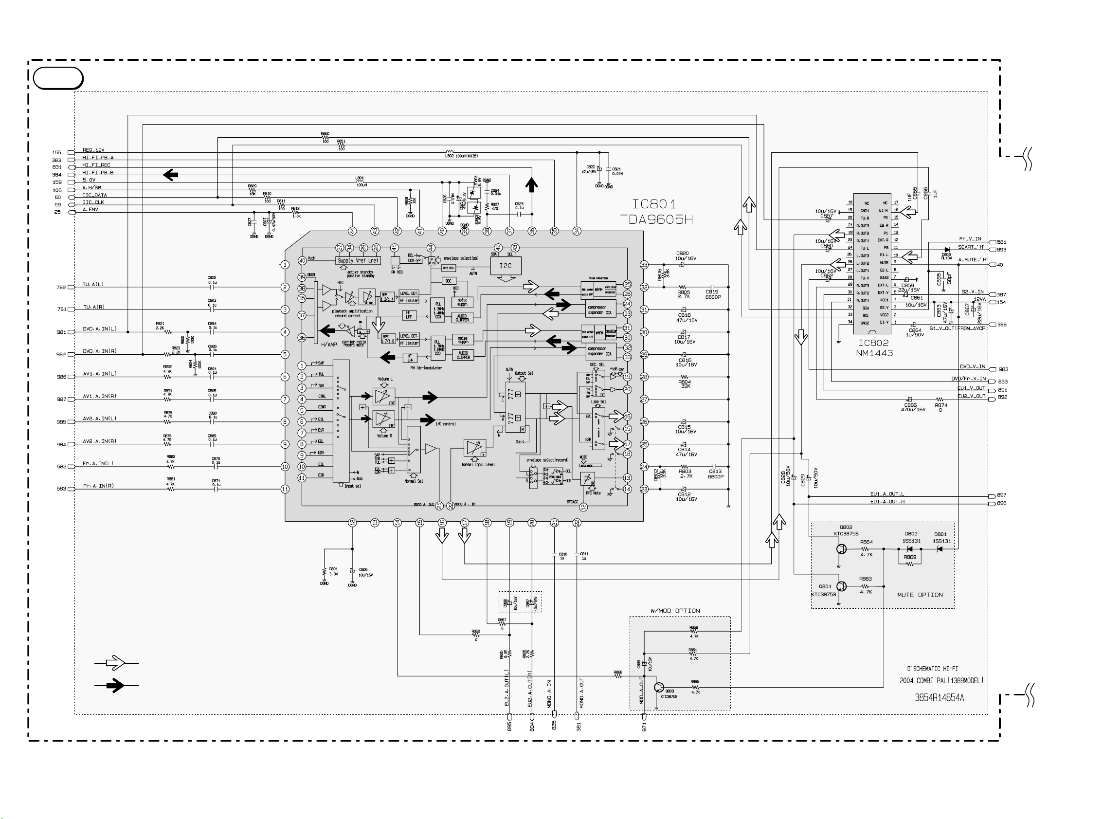
MAIN SCHEMATIC DIAGRAM - SCHEMA DE LA PLATINE PRINCIPALE - SCHALTBILD HAUPTPLATINE - SCHEMA DELLA PIASTRA PRINCIPALE- ESQUEMA DE LA PLATINA PRINCIPAL
MAIN Hi-Fi CIRCUIT DIAGRAM
PB
REC
Page 17
28
DTH6300
First issue 03 / 05 27
MAIN SCHEMATIC DIAGRAM - SCHEMA DE LA PLATINE PRINCIPALE - SCHALTBILD HAUPTPLATINE - SCHEMA DELLA PIASTRA PRINCIPALE- ESQUEMA DE LA PLATINA PRINCIPAL
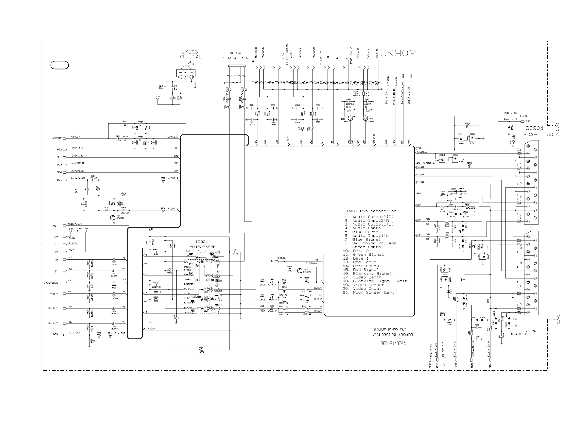
SCART (JACK) CIRCUIT DIAGRAM
MAIN
Page 18

29
DTH6300
30 First issue 03 / 05
MAIN SCHEMATIC DIAGRAM - SCHEMA DE LA PLATINE PRINCIPALE - SCHALTBILD HAUPTPLATINE - SCHEMA DELLA PIASTRA PRINCIPALE- ESQUEMA DE LA PLATINA PRINCIPAL
TU/IF, NICAM & A2 CIRCUIT DIAGRAM
MAIN
EE MODE(VIDEO)
TU MODE (AUDIO)
Page 19

32
DTH6300
First issue 03 / 05 31
MAIN SCHEMATIC DIAGRAM - SCHEMA DE LA PLATINE PRINCIPALE - SCHALTBILD HAUPTPLATINE - SCHEMA DELLA PIASTRA PRINCIPALE- ESQUEMA DE LA PLATINA PRINCIPAL
Some Models*
KEYBOARD
TIMER CIRCUIT DIAGRAM*
Page 20

33
DTH6300
34 First issue 03 / 05
MEASUREMENTS - MESURES - MESSUNGEN - MISURE ELABORAZIONE - MEDIDAS - TRATAMIENTO
( VCR )
CIRCUIT VOLTAGE CHART
MODE
PIN NO .
1
2
3
4
5
6
7
8
9
10
11
12
13
14
15
16
17
18
19
20
21
22
23
24
25
26
27
28
29
30
1
2
3
4
5
6
7
8
9
10
11
12
13
14
15
16
17
18
19
20
21
22
23
EE PB REC
IC201
2.36 V
2.4 V
3.5 V
2.43 V
0.002 V
0.4 V
0.003 V
0.003 V
2.87 V
2.36 V
3.16 V
2.3 V
2.98 V
3.2 V
0.15 V
0.124 V
2.23 V
1.84 V
4.71 V
4.72 V
4.72 V
2.37 V
2.37 V
0.182 V
0.46 V
1.95 V
3 V
4 V
3 V
3 V
2.35 V
2.35 V
3.49 V
2.41 V
0.005 V
3.7 V
0.003 V
0.003 V
2.85 V
2.35V
3.13 V
1.7 V
4 V
2.3 V
1.78 V
3.2 V
3.86 V
3.38 V
2.23 V
3.3 V
2.34 V
0.002 V
4.69 V
4.69 V
2.26 V
2.25 V
2.86 V
0.187 V
0.62 V
1.94 V
IC301
4.8 V
0.11 V
2.16 V
0.69 V
2.15 V
2.16 V
2.15 V
2.15 V
2.14 V
2.16 V
2.23 V
1.56 V
2.14 V
0.022 V
2.14 V
4.85 V
2.14 V
4.8 V
3.88 V
2.31 V
3.2 V
3.2 V
3 V
4.84 V
0.014 V
2.16 V
0.63 V
2.15 V
2.15 V
2.15 V
2.15 V
2.14 V
2.16 V
2.27 V
0.002 V
2.14 V
0.022 V
2.14 V
0.146 V
2.14 V
4.86 V
3.92 V
0.003 V
1.68 V
2.62 V
2.55 V
2.32 V
2.4 V
3.5 V
2.38 V
0.006 V
0.39 V
0.003 V
0.003 V
2.81 V
2.32 V
3 V
3.03 V
4 V
2.25 V
2.93 V
3.2 V
0.017 V
0.127 V
2.23 V
3.3 V
2.35 V
0.007 V
4.64 V
4.63 V
2.37 V
2.36 V
3 V
0.182 V
0.85 V
1.91 V
0.99 V
0.81 V
2.03 V
1.73 V
2.26 V
2.06 V
2.1 V
2.1 V
2.73 V
2.66 V
2.8 V
2.0 V
0.095 V
2.05 V
2.08 V
4.68 V
2.09 V
4.73 V
2.72 V
0.006 V
3.02 V
3.2 V
3.2 V
MODE
PIN NO .
24
25
26
27
28
29
30
31
32
33
34
35
36
37
38
39
40
41
42
43
44
45
46
47
48
49
50
51
52
53
54
55
56
57
58
59
60
61
62
63
64
65
66
67
68
69
70
71
72
73
74
75
76
77
78
EE PB REC
4.85 V
0.121 V
1.65 V
2.16 V
3.75 V
2.43 V
0.002 V
4.76 V
4.68 V
2.88 V
0.061 V
3.02 V
3.5 V
1.7 V
8.65 V
0.002 V
0.002 V
4.8 V
2.4 V
13.8 mV
2.5 V
2.6 V
4.14 V
3.3 V
2.97 V
1.93 V
0.002 V
1.93 V
2.33 V
1.93 V
5.14 V
2.24 V
1.95 V
2.9 V
1.47 V
1.8 V
0.087 V
1.8 V
0.002 V
1.71 V
0.002 V
0.005 V
4.8 V
4.7 V
7.75 V
5.55 V
4.84 V
2.21 V
2.45 V
2.38 V
2.4 V
1.58 V
2.44 V
2 V
3 V
4.85 V
3.4 V
1.25 V
2.1 V
3.7 V
2.46 V
0.002 V
4.58 V
4.58 V
2.86 V
0.06 V
2.34 V
2.84 V
1.76V
2.05 V
8.6 V
0.003 V
0.003 V
4.8 V
2.67 V
3.86 V
2.52 V
2.78 V
4.14 V
3.09 V
2.93 V
1.92 V
0.003 V
1.93 V
2.33 V
1.92 V
5.14 V
2.57 V
2.28 V
2.55 V
2.93 V
1.54 V
2.44 V
0.09 V
2.55 V
0.003 V
0.002 V
0.003 V
0.07 V
4.8 V
4.7 V
2.55 V
0.008 V
4.8 V
2.2 V
2.6 V
0.72 V
0.81 V
1.6 V
3.35 V
4.75 V
0.19 V
1.6 V
2.14 V
3.66 V
2.34 V
0.005 V
4.72 V
4.71 V
2.8 V
0.061 V
2.99 V
3.4 V
1.61 V
1.94 V
8.38 V
0.006 V
0.006 V
4.68 V
2.17 V
0.03 V
2.55 V
2.64 V
4.14 V
3.30 V
3.69 V
1.92 V
0.005 V
1.92 V
2.34 V
1.92 V
5.13 V
2.22 V
0.006 V
3.01 V
2.92 V
1.48 V
1.79 V
0.088 V
1.78 V
0.006 V
1.69 V
0.006 V
0.44 V
4.78 V
4.7 V
5.55 V
0.008 V
4.72 V
2.24 V
2.43 V
2.38 V
2.39 V
1.48 V
2.33 V
MODE
PIN NO.
79
80
81
82
83
84
85
86
87
88
89
90
91
92
93
94
95
96
97
98
99
100
1
2
3
4
5
6
7
8
9
10
11
12
13
14
15
16
17
18
19
20
21
22
23
24
1
2
3
4
5
6
7
EE PB REC
1.73 V
0.98 V
1.1 V
0.003 V
1.65 V
0.258 V
0.002 V
0.251 V
0.77 V
0.77 V
0.77 V
0.77 V
4.85 V
2.1 mV
1.7 V
1.7 V
1.7 V
1.7 V
0.002 V
2.16 V
2.16V
2.16 V
1.67 V
0.98 V
1.13 V
0.004 V
1.03 V
2.5 V
0.003 V
0.014 V
0.78 V
0.78 V
0.78 V
0.78 V
4.83 V
0.004 V
1.72 V
1.71 V
1.71 V
1.71 V
0.005 V
2.16 V
2.16 V
2.16 V
IC5F1
2.33 V
4.98 V
4.96 V
4.89 V
0.64 V
0.64 V
0.64 V
0.73 V
0.72 V
1.83 V
0.73 V
1.26 V
1.26 V
1.65 V
1.58 V
4.89 V
0.002 V
1.75 V
1.7 V
1.78 V
1.73 V
0.002 V
5 V
1 V
2.31 V
4.9 V
5 V
4.9 V
4.85 V
0.59 V
0.59 V
0.61 V
0.93 V
0.92 V
0.63 V
1.84 V
0.75 V
1.22 V
1.23 V
1.63 V
1.58 V
4.8 V
0.003 V
1.63 V
1.7 V
1.71 V
1.6 V
0.003 V
IC751
5.1 V
1.5 V
1.5 V
0.002 V
2.5 V
2.44 V
1.84 V
5.1 V
1.5 V
1.5 V
0.003 V
2.46 V
2. 44 V
1.89 V
2.51 V
4.46 V
1.15 V
0.006 V
1.41 V
0.014 V
1.38 V
1.98 V
0.78 V
0.77 V
0.77 V
0.77 V
4.74 V
0.006 V
3.94 V
3.93 V
3.92 V
3.94 V
0.006 V
2.21 V
2.25 V
2.31 V
2.3 V
4.9 V
5 V
4.9 V
4.8 V
0.6 V
0.6 V
0.6 V
0.96 V
0.91 V
0.92 V
1.8 V
0.72 V
1.2 V
1.1 V
1.54 V
1.42 V
4.8 V
0.003 V
1.5 V
1.5 V
1.5 V
1.41 V
0.003 V
5.08 V
1.51 V
1.5 V
0.003 V
2.46 V
2.43 V
2.06 V
MODE
PIN NO.
8
9
10
11
12
13
14
15
16
17
18
19
20
21
22
23
24
25
26
27
28
29
30
31
32
33
34
35
36
37
38
39
40
41
42
43
44
1
2
3
4
5
6
7
8
9
10
11
12
13
14
15
16
17
EE PB REC
1.86 V
1.86 V
0.002 V
5.12 V
1.75V
1.77 V
1.77 V
1.75 V
1.75 V
0.003 V
1.88 V
0.002 V
0.002 V
0.002 V
0.05 V
0.05 V
0.002 V
0.002 V
2.78 V
2.78 V
0.002 V
4.06 V
0.003 V
2.77 V
0.002 V
0.002 V
0.002 V
2.76 V
2.76 V
2.59 V
2.35 V
0.003 V
4.8 V
4.7 V
5 V
5.1 V
5.1 V
0.004 V
0.004 V
0.003 V
5.12 V
4.75 V
0.003 V
1.58 V
0.005 V
0.005 V
0.003 V
0.051 V
0.05 V
0.003 V
0.003 V
2.77 V
0.003 V
5.09 V
4.08 V
0.003 V
2.76 V
0.002 V
0.003 V
0.003 V
2.75 V
2.75 V
2.59 V
2.35 V
0.003 V
IC501
0.002 V
2.56 V
2.56 V
2.56 V
2.56 V
2.56 V
2.64 V
2.54 V
0.064 V
5.13 V
1.69 V
2.32 V
0.48 V
1.28 V
1.84 V
2.32 V
0.002 V
2.55 V
2.55 V
2.55 V
2.55 V
2.56 V
2.63 V
2.53 V
2.27 V
5.12 V
1.68 V
1.7 V
0.08 V
1.29 V
1.83 V
4.8 V
2.6 V
2.6 V
5 V
1.5 V
1.5 V
5 V
5.1 V
1.9 V
1.7 V
2 V
3 V
0.004 V
0.004 V
0.003 V
5.11 V
4.8 V
4.7 V
2.59 V
2.6 V
5 V
2.06 V
2 V
5 V
0.003 V
2 V
5.11 V
0.004 V
0.005 V
0.003 V
0.051 V
0.05 V
0.005 V
0.003 V
2.76 V
2.76 V
0.005 V
5.08 V
4.06 V
0.003 V
2.76 V
0.002 V
0.002 V
0.002 V
2.75 V
2.75 V
2.6 V
2.35 V
0.003 V
0.002 V
2.55 V
2.9 V
2 V
2.55 V
2.55 V
2.6 V
2.52 V
2.26 V
5.11 V
1.66 V
1.67 V
2.3 V
0.53 V
1.36 V
1,8 V
2.26 V
MODE
PIN NO .
18
19
20
21
22
23
24
25
26
27
28
29
30
31
32
33
34
35
36
37
38
39
40
41
42
43
44
45
46
47
48
49
50
51
52
53
54
55
56
57
58
59
60
61
62
63
64
65
66
67
68
69
70
71
72
EE PB REC
4.7 V
2.19 V
0.01 V
2.2 V
2.32 V
0.01 V
0.3 V
0.08 V
5.14 V
4.2 V
5.13 V
5.13 V
0.004 V
0.002 V
0.002 V
0.18 V
1.37 V
5.14 V
5.14 V
4.74 V
4.74 V
2.45 V
5 V
2.28 V
0.003 V
4.76 V
0.003 V
(-)0.001 V
0.003 V
0.003 V
0.003 V
5.14 V
5.1 V
4.38 V
0.031 V
0.003 V
5.1 V
5.1 V
5.1 V
0.002 V
0.003 V
4.8 V
4.7 V
4.7 V
5 V
1.8 V
5.1 V
1.78 V
5.1 V
0.004 V
0.001 V
0.001 V
5.14 V
5.14 V
0.028 V
4,7 V
3 V
0.009 V
2.2 V
2.3 V
0.009 V
2.84 V
3.4 V
5.13 V
4.16 v
5.13 V
5.13 V
0.002 V
0.002 V
0.002 V
0.18 V
1.3 V
5.13 V
5.13 V
4.73 V
4.75 V
4.9 V
0.003 V
1.55 V
0.003 V
4.75 V
0.003 V
(-)0.001 V
0.003 V
0.003 V
0.003 V
0~5 V
0.003 V
0.03 V
5.06 V
0.003 V
5 V
5.13 V
5,1 V
0.002 V
0.004 V
4.8 V
4.7 V
5 V
5 V
1.3 V
5 V
5.1 V
5.1 V
4.4 V
5.1 V
5.1 V
5.1 V
0.001 V
0.028 V
4.6 V
2.13 V
0.01 V
2.16 V
2.26 V
0.01 V
0.012 V
0.068 V
5.12 V
3.93 V
5.11 V
5.11 V
0.003 V
0.002 V
0.002 V
0.18 V
1.42 V
5.1 V
5.1 V
4.7 V
4.7 V
2.33V
4.96 V
1.42 V
0.004 V
4.73 V
0.004 V
(-)0.001 V
0.004 V
5 V
0.004 V
0.005~5 V
0.004 V
0.035 V
0.038 V
0.004 V
5 V
5.11 V
5.1 V
0.002 V
0.004 V
4.8 V
4.9 V
5 V
5 V
1.68 V
5 V
1.66 V
5.08 V
5.08 V
0.005 V
5.12 V
5.12 V
0.001 V
0.029 V
MODE
PIN NO .
73
74
75
76
77
78
79
80
81
82
83
84
85
86
87
88
89
90
91
92
93
94
95
96
97
98
99
100
101
102
103
104
105
106
107
108
109
110
111
112
1
2
3
4
5
6
7
8
9
10
11
12
13
14
EE PB REC
5 V
0.001 V
1.5 V
1.7 V
5.1 V
2.5 V
0.001 V
2.53 V
3.2 V
5.12 V
0.172 V
0.004 V
0.019 V
2.55 V
5.11 V
5.11 V
5.11 V
5.11 V
5.11 V
5.12 V
0.005 V
0.005 V
4.38 V
0.005 V
5.11 V
0.005 V
5.11 V
0.005 V
1.51 V
0.005 V
0.099 V
0.099 V
5.11 V
0.005 V
0.005 V
0.005 V
0.049 V
0.002 V
0.48 V
5.12 V
5.1 V
0.001 V
1.93 V
2.02 V
5.1 V
2.51 V
0.002 V
2.5 V
3.2 V
5.1 V
2.68 V
2.4 V
3.4 V
2.55 V
3.1 V
4.95 V
4.97 V
5 V
5.1 V
0.008~0.05 V
0.005 V
0.005 V
0.05 V
0.005 V
5.1 V
5.3 V
2.55 V
0.005 V
2.6 V
0.006 V
1.36 V
1.36 V
2.55 V
2.54 V
2.75 V
2.81 V
50.6 V
0.002 V
0.6 V
5.11 V
IC801
3.8 V
3.8 V
3.8 V
3.8 V
3.8 V
3.8 V
3.8 V
3.8 V
3.8 V
3.8 V
3.8 V
0.054 V
3.87 V
0.008 V
3.81 V
3.82 V
3.82 V
3.82 V
3.82 V
3.82 V
3.82 V
3.82 V
3.82 V
3.82 V
3.82 V
~
3.8 V
0.003 V
5.04 V
0.002 V
1.48 V
1.44 V
5.08 V
2.52 V
0.002 V
2.5 V
3.19 V
5.1 V
2.55 V
2.69 V
3.44 V
2.56 V
2.29 V
4.9 V
4.9 V
4.98 V
5.09 V
0.006 V
0.006 V
0.013 V
0.012 V
0.006 V
5.09 V
0.006 V
2.52 V
0.006 V
1.31 V
0.006 V
1.38 V
1.36 V
2.53 V
2.53 V
2.75 V
2.79 V
0.05 V
0.002 V
0.55 V
5.1 V
3.82 V
3.82 V
3.82 V
3.82 V
3.82 V
3.82 V
3.82 V
3.82 V
3.82 V
3.82 V
3.82 V
0.048 V
3.99 V
0.011 V
MODE
PIN NO .
15
16
17
18
19
20
21
22
23
24
25
26
27
28
29
30
31
32
33
34
35
36
37
38
39
40
41
42
43
44
1
2
3
4
5
6
7
8
9
10
11
12
13
14
15
16
17
18
19
20
21
22
23
24
EE PB REC
0.008 V
4.58 V
3.82 V
3.86 V
3.87 V
3.87 V
0.76 V
0.001 V
3.84 V
3.86 V
0.77 V
3.87 V
3.86 V
3.86 V
11.84 V
0.64 V
0.64 V
0.64 V
0.005 V
0.002 V
0.005 V
0.078 V
6 V
6 V
7 V
6 V
6 V
5 V
4.7 V
4.8 V
0.006 V
6.07 V
6.07 V
6.07 V
6.06 V
6.07 V
4.57 V
3.82 V
3.84 V
3.84 V
3.9 V
0.003 V
0.003 V
3.83 V
3.86 V
0.76V
3.87 V
3.87 V
3.86 V
11.76 V
0.44 V
0.62 V
0.63 V
0.008 V
0.005 V
5.07 V
0.92 V
4.7 V
4.8 V
3.3 V
IC802
3 V
2.93 V
11.8 V
2.74 V
11.8 V
2.74 V
11.23 V
0.008 V
5.54 V
0.008 V
0.002 V
0.002 V
(-)0.001 V
5.54 V
5.5V
5.6 V
5.5 V
5 V
5.5 V
5.5 V
5.5 V
5.5 V
5.6 V
5.6 V
5.6 V
11.76 V
2.74 V
11.75 V
2.75 V
5.5 V
5.56 V
5.5 V
0.006 V
5.5 V
11.15 V
5.5 V
0.01 V
5.5 V
0.009 V
5.5 V
0.003 V
0.005 V
0.001 V
5.5 V
5.59 V
5.59 V
5.51 V
5.5 V
0.01 V
6.07 V
6.08 V
0.11 V
0.028V
6.07 V
5.9 V
3.82 V
3.86 V
3.87 V
3.87 V
0.76 V
0.005 V
3.83 V
3.86 V
0.76 V
3.86 V
3.87 V
3.86 V
11.77 V
4.3 V
4.3 V
4.28 V
4.32 V
0.006 V
5.05 V
0.92 V
4.7 V
4.8 V
0.068 V
3.05 V
11.76 V
2.74 V
11.76 V
2.75 V
5.5 V
5.57 V
5.49 V
4.97 V
5.5 V
11.16 V
5.5 V
0.009 V
5.5 V
0.009 V
5.51 V
0.005 V
0.004 V
0.001 V
5.51 V
5.59 V
5.59 V
5.52 V
5.5 V
MODE
PIN NO.
25
26
27
28
29
30
31
32
33
34
EE PB REC
5.6 V
5.6 V
5.54 V
4.16 V
1.46 V
2.1 V
1.35 V
4.7 V
4.8 V
(-) 0.002 V
5.58 V
5.58 V
5.5 V
4.32 V
1.46 V
1.99 V
1.35 V
4.7 V
4.8 V
0.001 V
5.59 V
5.59 V
5.5 V
4.51 V
1.46 V
2.07 V
1.35 V
4.7 V
4.8 V
0.000 V
Page 21

36
DTH6300
First issue 03 / 05 35
BLOCK DIAGRAM - SCHEMA SYNOPTIQUE - BLOCKSCHALTBILD - SCHEMA A BLOCCHI - ESQUEMA DE BLOQUES
DVD PRINCIPAL
Overall Block Diagram
LOADING
5V/8V
SPINDLE
MOTOR
M
MOTOR
(FEEDING)
LOAD[+,-]
SLED
MOTOR
M
SL ED[+,-]
DISC
M
SP INDLE[+,-]
FOCUS[+,-]
PICK
UP
Pick-up
TRACK[+,-]
DV D : A,B,C,D,RF0
CD : A, B,C,D, E,F,RF0
CDMDI,DVDMDI
CDLD,DVDLD,SVREF21
XSFGN,XSFGP
HOMESW
INSW,OUTS W
CD_D VD, VR_CD,VR_DVD
OPU_SEL
CD_D VD_CT
VD33 D
VD18/VD33
IC602
MX29LV160T
2/4M
16/32BIT
FLASH ROM
19]
ROMAD[0:
ROMRD
ROMWR
ROMDAT A[0:7]
VD33 D
MA[00:11 ]
DMCL K
DQM
CA SJ
RA SJ
IC601
MTK MT1389
CS J
BA 0
BA 1
WE J
IC603
4M
16BIT
4BanK
SDRAM
RF+
MD[00:15]
CN603
RS232
Download
RS 232_R XD
IIC/VFD/ DA C_ SCK
IIC/VFD/ DA C_TX D
BCLK
LRCL K
DA CCLK
SER3,DAC_ML0
VD33D
IC606
S524A40X21
EEPROM
VD33D/5V
IC401
CS4392
2DAC
3V3M
DAC_RST
IC201
IP4504A
Motor Drive
AC 90V~240V
50HZ/60Hz
OPEN,C LO SE ,SLE GP ,SPINDLE,FOC US ,TRACK, SVREF
DR VS B
VF +
VF -
-27V A
5.2V A
5V
POWER
BOARD
12V
3.3V-M1
3.3V
3.3V- M
8V
U7
+12V
VD18
VD33,VD33D
3V3M
5.3VA
LED501
CLK DISPLAY
PWRCTL
5.2VA
M-RESET
VFD_RXD
IC501
KEY Input
5.2VA
74HCT244
S_ REQ
IC607
6MHz
M_REQ
27MHz
VIDE O_SW
IC505
RESET IC
RC601
R/C
TRIGGER
MPEG IC
D2_T [1:3]
SCART_16:9
RGB_SEL
JACK
5V
IC901
MM162 3XFBE
VIDEO BUFFER
CVBS
R/Pr G/ Y
B/Pb
YC_MIX
Y
C
TV_D AC[0:3]
IECDAOUT
COAXIAL
SPDIF
RS 232_TXD
L/R
+12V
IC602
MC4580
OP-AMP
L/R
Page 22

37
DTH6300
38 First issue 03 / 05
MAIN SCHEMATIC DIAGRAM - SCHEMA DE LA PLATINE PRINCIPALE - SCHALTBILD HAUPTPLATINE - SCHEMA DELLA PIASTRA PRINCIPALE- ESQUEMA DE LA PLATINA PRINCIPAL
DVD PART
MAIN SERVO
Page 23

40
DTH6300
First issue 03 / 05 39
MAIN SCHEMATIC DIAGRAM - SCHEMA DE LA PLATINE PRINCIPALE - SCHALTBILD HAUPTPLATINE - SCHEMA DELLA PIASTRA PRINCIPALE- ESQUEMA DE LA PLATINA PRINCIPAL
DVD PART
MAIN DVD AUDIO
Page 24

41
DTH6300
42 First issue 03 / 05
MAIN
1. SYSTEM CIRCUIT DIAGRAM
MAIN SCHEMATIC DIAGRAM - SCHEMA DE LA PLATINE PRINCIPALE - SCHALTBILD HAUPTPLATINE - SCHEMA DELLA PIASTRA PRINCIPALE- ESQUEMA DE LA PLATINA PRINCIPAL
DVD PART
Page 25

DTH6300
First issue 03 / 05 43
CIRCUIT VOLTAGE CHART
STOP PLAY STOP PLAY STOP PLAY STOP PLAY STOP PLAY
MODE
PIN NO .
2 2.54 2.3
3 2.55 2.3
4 2.53 2.3
5 2.56 2.35
6 2.54 2.43
7 2.56 2.42
8 0.001 0.001
9 1.39 1.38
10 3.5 3.37
11 0.004 0.004
12 0.002
13 3.97 3.96
14 3.97 3.96
15 3.99 2.71
16 3.96 5.21
17 3.98 4.04
18 3.96 3.88
19 8 8
20 1.38 1.38
21 1.38 1.73
22 1.38 1.38
23 3.24 3.22
24 5.07 4.87
25 2.59 2.46
26 2.55 2.48
27 2.59 2.47
28 2.52 2.43
1 3.25 3.24
2 3.25 3.23
3 0.002 1.21
4 1.62 1.61
5 1.62 1.61
6 1.57 1.56
7 0.001 0
8 3.27 3.26
9 3.27 3.26
10 0.001 0
11 5.02 4.81
12 2.38 2.3
13 4.9 0.001
14 2.4 2.36
15 2.4 2.36
16 0.001 0.001
17 5.1 4.93
18 2.4 2.35
19 2.4 2.36
20 4.9 0.001
1 5.8 5.72
2 5.8 5.73
3 5.8 5.73
40 0
5 5.8 5.72
IC201
IC401
IC402
MODE
PIN NO .
6 5.8 5.73
7 5.8 5.73
8 12.6 12.49
1 0.001 0.002
2 1.57 1.58
3 1.57 1.58
4 1.57 1.58
5 1.58 1.58
6 1.58 1.59
7 1.58 1.59
8 1.98 2.02
9 1.98 2.02
10 1.98 2.02
11 1.99 2.03
12 1.46 1.32
13 1.46 1.33
14 1.46 1.31
15 1.46 1.32
16 1.45 1.35
17 1.45 1.35
18 1.99 2.2
19 1.99 2.1
20 0 0.1
21 0 0
22 3.2 3.1
23 3.2 3.1
24 3.2 3.1
25 1.37 1.8
26 0.8 0.07
27 0 0.003
28 2.6 2.7
29 1.9 1
30 1.38 1.2
31 1.34 1.21
32 0.8 1.3
33 0.8 1.3
34 3 2.8
35 3.28 2.8
36 1.38 2.4
37 1.38 2.6
38 1.37 1.3
39 0.003 0
40 1.37 1.3
41 1.41 1.31
42 1.39 1.3
43 0.001 0
44 0.02 0.01
45 0.02 0.01
46 3.25 3.2
47 2.99 3
48 3.25 3.2
49 0 0.001
50 3.23 3.21
51 0.002 0.001
IC601
MODE MODE
PIN NO .
52 1.8 1.71
53 3.25 3.19
54 3.25 3.2
55 3.25 3.2
56 3.22 3.1
57 3.21 3.13
58 3.19 3.1
59 3.25 3.1
60 3.25 3.12
61 0.001 0.002
62 0 0.002
63 1.77 1.72
64 0 0.002
65 3.24 3.1
66 3.25 3.21
67 0.001 0.002
68 0.002 0.002
69 0.001 0.003
70 0.001 0.003
71 3.25 3.24
72 3.25 3.24
73 3.25 3.24
74 0.001 0.003
75 0 0.002
76 0.001 0.001
77 0.001 0.002
78 2.44 2.41
79 0.001 0.003
80 3.2 3.1
81 3.2 3.1
82 3.27 3.24
83 3.23 3.16
84 3.2 3.1
85 0.001 0.003
86 3 2 .91
87 3 2 .99
88 3 2.9
89 0.007 0.008
90 0.001 0.003
91 2.99 1.2
92 0.001 0.003
93 3.27 3.24
94 0.001 0.002
95 3.2 3.2
96 3.97 3.7
97 1.8 1.8
98 4.1 3.2
99 4.1 3.2
100 3.2 3.2
101 3.2 3.16
102 3.27 3.23
103 3.2 3.23
104 4 3.9
105 2.1 2.1
106 4.1 3.99
PIN NO .
107 3.2 3.21
108 3.25 3.21
109 0.02 0.03
110 5.1 5.15
111 4.2 3.6
112 4.2 3.68
113 2.6 2.5
114 3.2 3.1
115 1.6 1.5
116 0.001 0.003
117 0.4 0.02
118 1.8 1.7
119 0 0
120 0.9 0.8
121 1 0.8
122 1.8 1.8
123 1.38 1.31
124 1.23 1.2
125 1.3 1.25
126 0.34 0.35
127 3.25 3.2
128 1.8 1.81
129 2 1.9
130 1.04 0.8
131 1.8 1.75
132 0.002 0.003
133 0.001 0.9
134 0.002 0.001
135 1.06 0.99
136 3.24 3.2
137 3.06 3
138 3.17 3
139 3.1 3
140 3.26 3.1
141 3.26 3.1
142 3.04 3
143 1.27 1.12
144 0.002 0.003
145 1.57 1.6
146 0.04 0.04
147 1.47 1.39
148 0.002 0.003
149 1.67 1.55
150 1.59 1.6
151 1.8 1.7
152 0.02 0.01
153 0.02 0.01
154 3.25 3.14
155 1.7 3.24
156 0.4 0.04
157 0.002 0.003
158 0.003 0.003
159 0.003 0.003
160 0.02 0.04
161 0.001 0.003
PIN NO .
162 1.47 1.61
163 0.002 0.002
164 2.25 0.04
165 2.26 2.1
166 1.36 1.45
167 3.25 3.24
168 0.003 0.003
169 0.002 0
170 0.03 0.02
171 0.03 0.01
172 1.8 1.79
173 1.8 1.78
174 3.25 3.24
175 0.001 0.003
176 4 4.1
177 3.25 3.2
178 3.26 3.2
179 4.1 3.61
180 0.03 0.02
181 0.03 0.02
182 3.25 3.2
183 0.03 0.03
184 0.03 0.03
185 0.03 0.03
186 0.03 0.03
187 0.03 0.03
188 0.03 0.01
189 3.23 3.21
190 1.23 1.24
191 1.24 1.24
192 2.22 2.08
193 0 0.001
194 0.3 0.4
195 3.23 3.21
196 0.7 0.7
197 0 0.001
198 3.2 3.21
199 3.23 3.2
200 0.002 0.4
201 0.002 0.002
202 0.2 0.4
203 0.2 0.4
204 3.25 3.23
205 2.96 2.93
206 3.7 3.61
207 2.9 2.91
208 3.7 3.54
209 4 3.5
210 4 3.5
211 3.7 3.4
212 3.7 3.2
213 1.6 1.61
214 1.6 1.61
215 1.57 1.55
216 0.003 0.02
MODE
Page 26

DTH6300
44 First issue 03 / 05
CIRCUIT VOLTAGE CHART
STOP PLAY STOP PLAY STOP PLAY STOP PLAY STOP PLAY
MODE
PIN NO .
217 0 .003 0 .002
218 0 .003 1.2
219 0 .003 0.6
220 3 3.1
221 1.8 1.81
222 0 .005 1.2
223 0 0
224 0.3 0.01
225 1.6 1.61
226 0 0
227 1.8 1.8
228 0.6 0.7
229 0.6 0.7
230 1.37 1.1
231 1.34 1.12
232 0 0
233 1.8 1.8
234 3.1 3
235 1 1.7
236 1.3 1.67
237 0 0.001
238 0.9 0.4
239 3.1 3.07
240 0.1 0.1
241 0 0
242 0.01 0.1
243 0.01 0.1
244 3.1 3.01
245 1.09 1.65
246 1.35 1.36
247 0.01 0.1
248 1.5 3.07
249 0 0.001
250 0.01 0.24
251 0.01 0.24
252 1.48 1.52
253 1.47 1.51
254 1 1.04
255 0.9 0.98
256 3.2 3.18
1 0.002 0.2
2 3.2 0.4
3 3.2 3.07
4 3.2 3.2
5 3.2 3.01
6 3.2 0.5
7 3.2 0.5
8 3.2 2
9 0.002 0.002
10 0.01 0.009
11 3.2 3.2
12 5.1 5.1
13 3.27 3.26
14 3.27 3.26
IC602
MODE
PIN NO .
15 4.62 3.8
16 2.13 0.002
17 2.11 1.15
18 2.06 2.36
19 2.06 2.1
20 2.12 2.5
21 2.06 1.7
22 2.07 1.9
23 2.05 1.88
24 1.9 2
25 1.8 2
26 0 0.001
27 0.001 0
28 0 0
29 2.3 1.65
30 1.48 1.4
31 1.17 1.36
32 1.5 1.4
33 0.66 1.3
34 1.5 1.4
35 0.9 1
36 1.5 1.4
37 3.2 3.26
38 1.5 1.58
39 1.5 1.4
40 1.69 2
41 1.3 1.4
42 1.5 1.2
43 1.4 1.4
44 1.3 1.3
45 1.9 1.98
46 0.001 0.002
47 0.001 0.002
48 0 0.002
1 3.27 3.25
2 1.27 1.2
3 3.27 3.25
4 1.25 1.1
5 1.38 1.14
6 0.02 0.001
7 1.06 1.14
8 0.93 1.47
9 3.27 3.26
10 1 1.57
11 0.41 1.48
12 0.001 0.001
13 1.98 0.38
14 3.27 3.26
15 2.9 2.71
16 3.23 3.19
17 3.09 3
18 3.19 3.13
19 3.03 2.89
20 1.55 1.49
IC603
MODE
PIN NO .
21 0.71 1.2
22 0.03 0.007
23 0.16 0.22
24 1.38 1.39
25 1.36 1.37
26 1.37 1.37
27 3.27 3.26
28 0.002 0.001
29 1.36 1.95
30 2.28 1.46
31 2.25 2.25
32 1.49 1.68
33 0.01 0.01
34 0.02 0.007
35 0.004 0.05
36 0.02 0.01
37 1.03 0.72
38 1.71 1.71
39 2.59 2.7
40 0.01 0.05
41 0.002 0.01
42 1.33 1.1
43 3.27 3.26
44 1.35 1.11
45 1.33 1.02
46 0.002 0.001
47 1.36 0.92
48 1.3 0.92
49 3.27 3.26
50 1.48 1
51 1.91 0.5
52 0.002 0.001
53 0.33 1.47
54 0.002 0.001
1 0.002 0.001
2 0.002 0.001
3 0.002 0.001
4 0.002 0.001
5 3.27 3.26
6 3.27 3.26
7 0.002 0.001
8 3.27 3.26
1 0.002 0.002
2 3.27 3.24
3 0.002 0.002
4 0.008 3.24
5 0.002 0.001
6 2.26 0.78
7 0.002 0.001
8 2.26 3.24
9 0.002 0.001
10 0.001 0.001
11 3.12 2.56
IC606
IC607
PIN NO .
12 2.45 5.14
13 2.94 2.55
14 2.44 1.25
15 2.82 2.65
16 0.002 5.11
17 2.96 2.65
18 0.002 5.11
19 0.001 0.001
20 5.24 5.14
1 5.09 4.9
2 2.41 2.3
3 5.09 4.9
4 1.17 1.13
5 0.002 0.001
6 1.56 1.62
7 0.002 0.001
8 2.46 2.37
9 0.001 0.002
10 1.14 1.31
11 0.05 0.05
12 2.37 2.29
13 5.09 4.9
14 2.41 2.32
15 0.001 0.001
16 2.46 2.38
17 0.002 0.002
18 2.35 2.3
19 0.002 0.001
20 1.2 1.56
21 1.7 2.17
22 0.002 0.002
23 1.69 2.14
24 0.03 0.03
25 0.03 0.03
26 2.47 2.38
27 0.03 0.03
28 5.09 4.89
1 2.26 2.1
2 5 5.04
3 5.07 5.05
4 5.02 5
5 4.6 4.25
6 1.7 2.54
7 1.35 2.49
8 1.43 2.3
9 1.81 2.47
10 1.8 2.48
11 1.75 2.44
12 1.52 0.77
13 0.8 0.83
14 1.14 1.63
15 2.1 1.79
16 2.11 1.81
IC901
IC5F1
MODEMODE
PIN NO .
17 2.17 1.78
18 4.61 4.25
19 0.002 0.002
20 2.2 1.82
21 2.2 1.79
22 2.23 1.82
23 2.23 1.9
24 0.002 0.002
Page 27

46
DTH6300
First issue 03 / 05 45
POWER SUPPLY CIRCUIT BOARD - CIRCUIT IMPRIME DE L’ALIMENTATION
LEITERPLATTE NETZTEIL - PIASTRA DEI CIRCUITI DI ALIMENTAZIONE
PLATINA ALIMENTACIÓN
KEYBOARD / DISPLAY / CLOCK CIRCUIT BOARD
CIRCUIT IMPRIME PLATINE COMMANDES / AFFICHEUR / HORLOGE
LEITERPLATTE BEDIENTEIL / ANZEIGE / UHRENPLATTE
PIASTRA TASTIERA / INDICATORE / OROLOGIO
PLATINA MANDOS / INDICADOR / RELOJ
KDB P.C.B BOARD *
TIMER PC BOARD *
Some Models*
Page 28

47
DTH6300
48 First issue 03 / 05
Component side - Côté composants - Bestückungsseite Lato componenti - Lado componentes
MAIN BOARD - PLATINE PRINCIPALE - CHASSIS GRUNDPLATTE - PIASTRA PRINCIPALE - PLATINA PRINCIPAL
Page 29

50
DTH6300
First issue 03 / 05 49
COMPONENTS LOCATION - LOCALISATION DES ELEMENTS - LAGE DER BAUTEILE LOCALIZZAZIONE DEGLI ELEMENTI - LOCALIZACION DE LOS COMPONENTES
COMPONENT SIDE - COTÉ COMPOSANTS - BESTÜCKUNGSSEITE - LATO COMPONENTI - LADO COMPONENTES
* SOLDER SIDE
Page 30

51
DTH6300
52 First issue 03 / 05
Solder side - côté cuivre - Lötseite - Lato saldature -Lado del cobre
MAIN BOARD - PLATINE PRINCIPALE - CHASSIS GRUNDPLATTE - PIASTRA PRINCIPALE - PLATINA PRINCIPAL
Page 31

54
DTH6300
First issue 03 / 05 53
5
4
3
2
6
9
10
8
12
18
16
19
17
13
15
11
1
33
14
7
15
35
• Top View
• Bottom View
21
21
24
23
22
31
32
31
32
25
34
28
27
29
20
26
30
24
1 Drum Assembly 3 screws A-1 T
2 Plate Top 2 hooks A-2 T
2 3 Holder Assembly CST 6 chasses A-2 T
2,3 4 Gear Assembly Rack F/L 1 hook A-2 T
2,3,4 5 Opener Door Chassis Hole A-2 T
2,3,4,5 6 Arm Assembly F/L Chassis Hole A-2 T
7 Lever Assembly S/W Chassis Hole, A-2 T
1 hook
8 Motor Assembly L/D 1 screw A-3 T
9 Gear Wheel 2 hooks A-3 T
10 Arm Assembly Cleaner Chassis Embossing A-3 T
11 Head F/E Chassis Embossing A-3 T
12 Base Assembly A/C Head 1 screw A-3 T
2,3 13 Brake Assembly T 1 hook A-4 T
2,3 14 Arm Assembly Tension 1 hook A-4 T
2,3,13,14 15 Reel S / Reel T Shaft A-4 T
16 Base Assembly P4 Chassis Embossing A-5 T
17 Opener Lid Chassis Embossing A-5 T
17 18 Arm Assembly Pinch Shaft A-5 T
17 19 Arm T/up 1 hook A-5 T
20 Supporter, capstan Chassis Hole A-6 B
17,18 21 Belt Capstan/Motor Capstan 3 screws A-6 B
22 Lever F/R Locking Tab A-6 B
21, 22 23 Clutch Assembly D37 Washer A-6 B
24 Gear Drive/Gear Cam Washer/Hook A-7 B
25 Gear Sector Hook A-7 B
21 26 Brake Assembly Capstan Chassis Hole A-7 B
21,22,23, 27 Plate Slider Chassis Guide A-7 B
24,2526
21,22,23, 28 Lever Tension 1 Hook A7 B
24,2526,27
21,22,23, 29 Lever Spring 1 Hook A-7 B
24,2526,27
21,22,23, 30 Lever Brake 1 Hook A-7 B
24,2526,27
25 31 Gear Assembly P2/ Bass A-8 B
Gear Assembly P3
2, 3, 14, 32 Base Assembly P2 6 Chasses A-8 B
25, 31 /Base Assembly P3
25, 31 33 Base Loading 3 Hooks A-8 B
2,3,14 34 Base Tension Chassis Embossing A-9 T
35 Arm Assembly Idler Jog Locking Tab A-9 T
Parts fir stly
Disassemble d
Order Of Dis-
assembled
Part Fixing Type
Ref.
Draw-
ings
Posit
ion
NOTE : Assemb ly order is a rever se of
disassemb ly order.
(1) For assembly, check the assembly mode is accurate.
(2) Parts firstly disassembled indicate parts firstly disassem-
bled in disassembly of related parts.
T:Top, B:Bottom
POSITION DRAWING OF DECK MECHANISM
DISASSEMBLY AND ASSEMBLY OF DECK MECHANISM
Drum Assembly
Cable Flat
(Fig. A-1-1)
Fig. A-1
1. Disassembly of Drum Assembly
(Figure A-1)
1) Separate cable flat from the Drum FPC and the Capstan
Motor.
2) Release 3 screws (S1) on the bottom side of the chassis,
and separate the drum assembly.
3) Release the hooks (H1, H2) and separate both the holder
FPC and the Cap FPC (disassemble if necessary).
(S1)
(S1)
(S1)
H2
H1
Holder FPC
Cautions in assembly of FPC
Drum FPC
Holder FPC
Assembly shape seen in the reverse direction
Cap, FPC
Cap FPC
Page 32

55
DTH6300
56 First issue 03 / 05
DISASSEMBLY AND ASSEMBLY OF DECK MECHANISM
DISASSEMBLY AND ASSEMBLY OF DECK MECHANISM
(H4)
(B')
Plate Top
(Fig. A-2-1)
Arm Assembly F/L
(Fig. A-2-5)
Lever Assembly S/W
(Fig. A-2-6)
(B)
(C)
Holder Assembly CST
(Fig. A-2-2)
(E)
(E)
2. Disassembly of Plate Top (Fig. A-2-1)
1) Separate the right part while leaning back the (B) part of
the plate top toward the arrow direction.
2) Separate the left part while leaning back the (B’) part of
the plate top toward the arrow direction.
(Tool used: Tool such as (-) driver, auger, etc with pointed
or flat end)
CAUTIONS
Assemble while pressing the (C), (C’) part after corresponding them as in drawing.
(C')
(C)
(B')
(B)
3. Holder Assembly CST (Fig. A-2-2)
1) Firstly separate the left part from the groove on the (D)
part of chassis while moving the holder assembly CST
toward the arrow direction.
Holder Assembly CST
(D)
Chassis
4. Disassembly of Gear Assembly
Rack F/L (Fig. A-2-3)
1) Separate the hook (H3) while leaning ahead the hook (3)
after moving the gear assembly rack F/L toward the arrow
(A) direction.
2) Separate the gear assembly rack F/L toward the arrow (B)
direction.
CAUTIONS
For the assembly, correspond the gear part of gear assembly rack F/L to the gear drive.
Gear Rack F/L
Gear Drive
5. Opener Door (Fig. A-2-4)
1) Separate the opener door ahead from the guide hole of
chassis while turning it clockwise.
6. Arm Assembly F/L (Fig. A-2-5)
1) Firstly separate the left part of the arm assembly F/L from
the groove of chassis while pushing the arm assembly F/L
toward the arrow direction.
2) Separate the right part from the groove of chassis.).
7. Lever Assembly S/W (Fig. A-2-6)
1) Separate the lever assembly S/W while pushing it toward
the arrow direction after removing the hook (4) on the left
side of chassis.
Fig. A-2
Gear Assembly Rack F/L
(Fig. A-2-3)
Opener Door
(Fig. A-2-4)
(A)
(H3)
(B)
2) Separate the right part from each groove of chassis
CAUTIONS
Assemble by inserting the left part after firstly inserting the
(E) part of the holder assembly CST into the groove on the
(E’) part of chassis.
Chassis
(H4)
Page 33

DTH6300
First issue 03 / 05 57
DISASSEMBLY AND ASSEMBLY OF DECK MECHANISM
Arm Assembly Cleaner
Base Assembly A/C Head
(Fig. A-3-5)
(A)
(S5)
(Fig. A-3-3)
(A)
(H5)
Gear Wheel
(Fig. A-3-2)
Motor Assembly L/ D
(Fig. A-3-1)
Head F/E
(Fig. A-3-4)
Fig. A-3
8. Motor Assembly L/D (Fig. A-3-1)
1) Take the connector (C1) connected to the Capstan motor
PCB out.
2) Remove a screw (S4) of the chassis (S4) and step backward, and disassemble it while holding it up.
9. Gear Wheel (Fig. A-3-2)
1) Release the hook (H5) of the gear wheel and disassemble
it upward.
(C1)
(S4)
10. Arm Assembly Cleaner (Fig. A-3-3)
1) Separate the (A) part of Fig. A-3-1 from the embossing of
chassis, and hold it up while turning it anti-clockwise.
11. Head F/E (Fig. A-3-4)
1) Separate the (A) part of the head F/E from the embossing of chassis, and hold it up while turning it anti-clockwise.
12. Base Assembly A/C Head (Fig. A-3-5)
1) Release a screw (S5) and disassemble while holding it up.
Page 34

DTH6300
58 First issue 03 / 05
DISASSEMBLY AND ASSEMBLY OF DECK MECHANISM
Arm Assembly Tension
(Fig. A-4-2)
(H7)
Reel S
Spring Tension
(Fig. A-4-3)
Reel T
(Fig. A-4-3)
(H8)
Spring Tension
Fig. A-4
Brake Assembly T
(Fig. A-4-1)
(H6)
13. Brake Assembly T (Fig. A-4-1)
1) Release the spring tension from the lever spring hook
(H6).
2) Disassemble the brake assembly T while holding it
upward.
14. Arm Assembly Tension (Fig. A-4-2)
1) Release the spring tension the hook (H7) from the arm
assembly tension.
2) After releasing the hook (H8) of the base tension, separate it while holding it up.
CAUTIONS
Spring used for both brake assembly T and arm assembly
tension is used (2EA used).
15. Reel S/Reel T (Fig. A-4-3)
1) Disassemble the reel S/ reel T while holding it up (comparison between Reel S and Reel T)
Reel S Reel T
Page 35

DTH6300
First issue 03 / 05 59
DISASSEMBLY AND ASSEMBLY OF DECK MECHANISM
Opener Lid
(Fig. A-5-2)
(B)
Arm Assembly Pinch
(Fig. A-5-3)
(C)
Base Assembly P4
(Fig. A-5-1)
(A)
(C)
(H9)
Arm T/up
(Fig. A-5-4)
Chassis
Fig. A-5
16. Base Assembly P4 (Fig. A-5-1)
1) Release the (A) part of the base assembly P4 from the
embossing of chassis.
2) Hold the base assembly P4 up while turning it anti-clockwise.
17. Opener Lid (Fig. A-5-2)
1) Release the (B) part of the opener lid from the embossing
of chassis.
2) Disassemble the opener lid upward while turning it anticlockwise.
18. Arm Assembly Pinch (Fig. A-5-3))
1) Hold the arm assembly pinch up.
19. Arm T/up (Fig. A-5-4)
1) Turn the arm T/up to release the anchor jaw (H9) part of
chassis and then hold it upward.
CAUTIONS
For the assembly, check the (C) part of the arm assembly
pinch is assembled as in drawing.
- REVERSE THE MECHANISM.
Page 36

DTH6300
60 First issue 03 / 05
DISASSEMBLY AND ASSEMBLY OF DECK MECHANISM
Suppoter Capstan
(Fig. A-6-1)
Belt Capstan
(Fig. A-6-2)
Motor Capstan
(Fig. A-6-3)
(L1)
(Fig. A-6-4)
(L1)
Lever F/R
Washer(W1)
Clutch Assembly D3 7
(Fig. A-6-5)
(S6)
Fig. A-6
20. Supporter , Capstan (Fig. A-6-1)
1) Turn the supporter and Capstan by 90 deg. clockwise
with a driver for disassembly.
21. Belt Capstan (Fig. A-6-2) /
Motor Capstan (Fig. A-6-3)
1) Separate the belt Capstan.
2) Undo 3 screws (S6) on the bottom side of chassis and disassemble it upward.
Chassis
22. Lever F/R (Fig. A-6-4)
1) Release the locking tab (L1) and then disassemble it
upward.
23. Clutch Assembly D37 (Fig. A-6-5)
1) Remove the washer (W1) and then disassemble it
upward.
Page 37

DTH6300
First issue 03 / 05 61
DISASSEMBLY AND ASSEMBLY OF DECK MECHANISM
Gear Cam Hole(B )
Gear Cam Hole(C )
Gear Drive Hole(A )
(H10)
(Fig. A-7-2)
(W2)
Gear Cam
Washer (W2)
Gear Drive
(Fig. A-7-1)
Lever Brack
(Fig. A-7-8)
(L2)
(H11)
Gear Sector
(Fig. A-7-3)
Brake Assembly Capstan
(Fig. A-7-4)
(Fig. A-7-5)
(B)
(Fig. A-7-7)
(A)
Plate Slider
Lever Tension
(Fig. A-7-6)
Lever sprin g
Base Loadin g
Fig. A-7
24. Gear Drive (Fig. A-7-1)/
Gear Cam (Fig. A-7-2)
1) Remove the washer (W2) and then disassemble the gear
drive.
2) Release the hook (H10) of the gear cam and then disas-
semble it upward.
CAUTIONS
For the assembly, adjust both the gear driver hole (A) and the
gear cam hole (B) straightly and then correspond the gear
cam hole (C) to the chassis hole.
25. Gear Sector (Fig. A-7-3)
1) Release the hook (H11) of the gear sector and then hold
the gear sector upward.
26. Brake Assembly Capstan (Fig. A-7-4)
Chassis
1) Release the locking tab (L2) on the bottom side of the
plate slider and then disassemble it upward.
27. Plate Slider (Fig. A-7-5)
1) Disassemble the plate slider while holding it up.
28. Lever Tension (Fig. A-7-6)
1) Release the lever tension from the guide (A) of chassis
while turning it anti-clockwise.
2) Disassemble the lever tension while holding it up.
29. Lever Spring (Fig. A-7-7)
1) Release the (B) part of the lever spring from the guide
(A) of chassis while turning it anti-clockwise.
2) Disassemble the lever tension while holding it up.
30. Lever Brake (Fig. A-7-8)
1) Disassemble the lever brake while holding it up.
Page 38

DTH6300
62 First issue 03 / 05
DECK MECHANISM DISASSEMBLY
Gear assembly P2 Hole
Gear assembly P3 Hole
Lever Tension Boss
Plate slider Hole(B)
(H12)
(H14)
Gear Assembly P3
(Fig. A-8-2)
Gear Assembly P2
(Fig. A-8-1)
(H13)
Base Loading
(Fig. A-8-5)
Chassis
Base Assembly P3
(Fig. A-8-4)
Fig. A-8
31. Gear Assembly P2 (Fig. A-8-1)/
Gear Assembly P3 (Fig. A-8-2)
1) Hold the gear assembly P2 upward.
2) Hold the gear assembly P3 upward.
CAUTIONS
For the assembly, check the holes of both the gear assembly
P2 and the P3 are adjusted straightly, and then correspond
the gear section groove (A) to the plate slider hole (B).
(B)
Base Assembly P2
(A)
(Fig. A-8-3)
32. Base Assembly P2 (Fig. A-8-3)/
Base Assembly P3 (Fig. A-8-4)
1) Disassemble the base assembly P2 downward while mov-
ing it toward the arrow (A) direction along with the guide
hole of chassis.
2) Disassemble the base assembly P2 downward while mov-
ing it toward the arrow (B) direction along with the guide
hole of chassis.
33. Base Loading (Fig. A-8-5)
1) Release 3 hooks (H12, 13, 14) of the base loading, and
then disassemble them upward.
- Reverse the mechanism.
Page 39

DTH6300
First issue 03 / 05 63
DISASSEMBLY AND ASSEMBLY OF DECK MECHANISM
Base Tension
(Fig. A-9-1)
(A)
(B) (C)
Arm Assembly Idler Jog
(Fig. A-9-2)
(D)
Fig. A-9
34. Base Tension (Fig. A-9-1)
1) Release the (A) part of the base tension from the
embossing of chassis.
2) Hold the base tension upward while turning it anti-clockwise.
Chassis
35. Arm assembly Idler Jog (Fig. A-9-2)
1) Push both (B), (C) parts in Fig. A-9-2 toward the arrow
direction.
2) Disassemble the arm assembly idler upward.
CAUTIONS
Take care to ensure that the (D) part in the drawing is not
hung to chassis in disassembly.
Page 40

DTH6300
64 First issue 03 / 05
DECK MECHANISM ADJUSTMENT
• Fixtures and Tools for Service
1. Cassette Torque Meter
2. Alignment tape 3. Torque gaug e
600g.Cm ATG
30
0
S
-
T
250
H
V
-
200
K
R
150
S
S
RK
V
ID
E
O
C
A
H
S
V
T
-
-
S
K
T
E
R
T
0
T
T
S
E
O
50
R
0
M
E
T
V
H
T
-3
0
50
Q
U
E
E
R
3
100
150
200
250
3
00
4. Torque gauge adaptor 5. Post height adjusting driver 6. + Type driver (ø5)
Page 41

DTH6300
First issue 03 / 05 65
DECK MECHANISM ADJUSTMENT
1. Mechanism Assembly Mode Check
Purpose of adjustment : To make tools normall y operate by positioning tools accurately .
Fixtures and tools used VCR (VCP) status Checking Position
• Blank Tape (empty tape)
1) Turn the VCR on and take the tape out by pressing the
eject button.
2) Separate both top cover and plate top, and check both
the hole (A) of gear cam and the hole (A’) of chassis correspond (Fig. C-2).
3) If it is done as in the paragraph 2): Turn the gear cam as
in No.2) after mantling the motor assembly L/D.
• Eject Mode
(with cassette withdrawn)
CHECK DIAGRAM
BOTTOM VIEW
• Mechanism and Mode Switch
4) Undo the screw fixing the deck and the main frame, and
separate the deck assembly. Check both the hole (A) of
gear cam and the hole (A’) of chassis correspond (Fig.
C-1).
5) Check the mode S/W on the main P.C. board locates at
a proper position as in (B) of the Fig. (C-1).
6) Connect the deck to the main P.C. board and perform all
types of test.
Gear Cam
(B)
(C)
Gear Drive
Correspondence of the gear cam hole (O)
and the gear drive hole (O)
Mode S/W
TOP VIEW
Fig. C-1
Fig. C-2
Motor Assembly L/D
Gear Cam
(A')
Chassis Hole
(A)
Gear Cam Hole
Page 42

DTH6300
66 First issue 03 / 05
DECK MECHANISM ADJUSTMENT
2. Previous Preparation for Deck Adjustment
(Preparation to load the VCR (VCP) with cassette tape not inserted)
1) Take the power cord from the consent.
2) Separate the top cover and the plate assembly top.
3) Insert the power cord into again.
4) Turn the VCR (VCP) on and load the cassette while pushing the lever stopper of the holder assembly CST backward. In this case, clog both holes on the housing
If doing so, proceeding to the stop mode is done. In this
status, input signals of all modes can be received.
However, operation of the Rewind and the Review is
impossible since the take-up reel remains at stop status
and so cannot detect the reel pulse (however, possible for
several seconds).
rail part of chassis to prevent detection of the end sensor.
3. Torque Measuring
Purpose of Measuring : To measure and check the reel torque on the take-up part and the
supply part that performs basic operation of the VCR (VCP) for
smoothl y forwarding the tape.
Measure and check followings when the tape is not smoothly
wound or the tape velocity is abnormally pr oceeded:
VCR (VCP) status Measuring methodFixtures and tools used
• Torque Gauge
(600 g.cm ATG)
• Torque Gauge Adaptor
• Cassette Torque Meter
SRK-VHT-303
• Play (FF) or Review
(REW) Mode
• Try to operate the VCR (VCP) per mode with the
tape not inserted (See ‘2. Prior Preparation for
Deck Adjustment).
• Measure after adhering and fixing the torque
gauge adaptor to the torque gauge (Fig. C-3-1)
• Read scale of the supply or take-up part of the
cassette torque meter (Fig. C-3-2).
Item
Fast forward Torque
Rewind Torque
Play Take-Up Torque
Review Torque
Fast Forward
Rewind
Play
Review
Mode Instruments Reel Measured Measuring Value
Torque Gauge
Torque Gauge
VHT-303
VHT-303
Take-Up Reel
Supply Reel
Take-Up Reel
Supply Reel
NOTE
Adhere the torque gauge adaptor to the torque gauge for measuring the value.
• Cassette Torque Meter (SRK-VHT-303)• Torque Gauge (600g.cm ATG)
Torque Gauge
Torque Gauge
Adaptor
More than 400g°cm
More than 400g°cm
40~100g°cm
120~210g°cm
3
0
0
S
-
T
2
5
0
H
V
-
2
0
0
K
R
15
S
0
S
RK
V
ID
E
O
C
A
H
S
V
T
-
-
S
K
T
E
R
T
0
T
TO
S
E
5
0
R
0
M
E
T
E
V
H
T
-30
3
5
QU
R
0
E
1
0
0
1
50
2
0
0
2
5
0
3
00
Reel Table
Fig. C-3-2Fig. C-3-1
Page 43

DTH6300
First issue 03 / 05 67
DECK MECHANISM ADJUSTMENT
4. Guide Roller Height Adjustment
Purpose of adjustment :To ensure that the bottom surface of the tape can travel along with
the tape lead line of the lower drum by constantly and adjusting
and maintaining the height of the tape.
4-1. Prior Adjustment
Fixtures and tools used VCR (VCP) status Adjustment position
• Post Height Adjusting
Driver
• Play or Review Mode
Adjustment Procedure
1) Travel the tape and check the bottom surface of the tape
travels along with the guide line of the lower drum.
2) If the tape travels toward the lower part of guide line on
the lower drum, turn the guide roller height adjusting
screw to the left
3) If it travels to the upper part, turn it to the right.
4) Adjust the height of the guide roller to ensure that the
tape is guided on the guide line of the lower drum at the
inlet/outlet of the drum. (Fig. C-4-1)
4-2. Fine Adjustment
Fixtures and tools used
• Oscilloscope
• Standard test tape
• Post height adjusting
driver
Measuring tools and
connection position
• CH-1: PB RF Envelope
• CH-2: NTSC : SW 30Hz
PAL : SW 25Hz
• Head switching output
point
• RF Envelope output
point
1) Play the standard test tape after connecting the probe of
oscilloscope to the RF envelope output point and the
head switching output point.
2) Tracking control (playback) : Locate it at the center
(Set the RF output to the maximum value via the tracking control when such adjustment is completed after the
drum assembly is replaced.)
3) Height adjusting screw: Flatten the RF waveform.
(Fig. C-4-2)
4) Move the tracking control (playback) to the right/left.
(Fig. C-4-3)
5) Check the start and the end of the RF output reduction
width are constant.
• The guide roller height adjusting screw on the
supply guide roller and the take-up guide roller
ADJUSTMENT DIAGRAM
GUIDE ROLLER
HEIGHT
ADJUSTMENT SCREW
Fig. C-4-1
VCR (VCP) status Adjustment position
• Play the standard test
tape.
• Guide roller height
adjusting screw
Waveform
P2 POST ADJUSTMENT
Flatten the waveform by
P3 POST ADJUSTMENT
Fig. C-4-2
When the tracking control
locates at the center.
lightly turning the
guide roller height adjustment screw.
When turning the tracking
control to both sides.
Fig. C-4-2
CAUTIONS
There must exist no crumpling and folding of the tape due
to excess adjustment or insufficient adjustment.
Connection Diagram
OSCILLOSCOPE
RF ENVELOPE OUTPUT POINT
CH-1 CH-2
HEAD RF SWITCHING OUTPUT POINT
Page 44

DTH6300
68 First issue 03 / 05
DECK MECHANISM ADJUSTMENT
5. Audio/Control (A/C) Head Adjustment
Purpose of adjustment : To ensure that audio and control signals can be recorded and
played according to the contract tract by constantly maintaining
distance between tape and head, and tape tension between the P3
post and the P4 post.
5-1. Prior Adjustment (performed only when no audio output appears in play of the standard test tape)
Fixtures and tools used VCR (VCP) status Adjustment position
• Blank Tape
(Empty Tape)
• Driver (+) Type ø 5
• Play the blank tape
(empty tape).
Adjustment Procedure/Adjustment Diagrams
1) Basically use the A/C head assembly adjusted as in
SPEC.
2) Check there is crumpling and folding of the tape around
the A/C head. If it is, Turn and adjust the tilt adjusting
screw to ensure that the tape corresponds to the bottom
guide of the P4, and recheck the tape path after proceeding play for 4-5 seconds.
8.3
A/C Head Base
Fig. C-5-1
• Tilt adjusting screw (C)
• Height adjusting screw (B)
• Azimuth adjusting screw (A)
3) Where the tape bottom is not equal to Fig. C-5-3, Adjust
the height by using the height adjusting screw (B) and
then readjust it by using the tilt adjusting screw (C).
CAUTIONS
Always check the height of the A/C head since most ideal
height of A/C head can be obtained when the bottom part
of the tape is away 0.2 ~ 0.25mm from the bottom part of
the A/C head.
A/C Head
P4
Tape
0.2~0.25mm
Tape
Fig. C-5-3
Azimuth
Adjustment
Screw(A)
X-Value Adjustment
Hole
Fixed Screw
Tilt Adjustment
Screw(C)
Height Adjustment
Screw(B)
A/C Head Assembly
Fig. C-5-2
Page 45

DTH6300
First issue 03 / 05 69
DECK MECHANISM ADJUSTMENT
5-2. Tape Path Check between Pinch Roller and
Take up Guide (Check in the Rev Mode)
1) Check the tape pass status between the pinch roller and
the take-up guide.(Check there is crumpling of the tape
pass and folding of the take-up guide.)
1) (1) When holding of the take-up guide bottom occurs
Turn the tilt adjusting screw (C) clockwise and travel it
stably to ensure there is no crumbling or folding of the
tape.
1) (2) When holding of the take-up guide top occurs
Turn the tilt adjusting screw (C) anti-clockwise and
travel it stably to ensure there is no crumbling or folding of the tape.
1) 2) Check there is folding of the tape at the bottom or top
of the take-up guide in cutting-off the REV mode
CAUTIONS
If the RF waveform is changed after adjusting the A/C head,
perform fine adjustment to ensure the RF waveform is flattened.
5-3. Fine Adjustment (Azimuth Adjustment )
Fixtures and tools used Connection position VCR (VCP) status Adjustment position
• Oscilloscope
• Standard test tape
(only for SP)
• Driver (+) Type Ø 4
Adjustment Procedure
1) Connect the probe of Oscilloscope to the audio output
jack.
2) Ensure that Audio 1KHz, 7KHz output is flattened at the
maximization point by adjusting the Azimuth adjusting
screw (A).
• Audio Output Jack • Play the standard test
• Tape, 1KHz, 7KHz.
1KHz
A: Maxim um
Fig. C-5-4
• Azimuth Adjusting
Screw (A)
• Height Adjusting Screw
(B)
B: Minimum
7KHz
6. X-distance Adjustment
Purpose of adjustment : To maintain compatibility with other VCR (VCP).
Fixtures and tools used Connection position VCR (VCP) status Adjustment position
• Oscilloscope
• Standard test tape
(only for SP)
• Driver (+) Type Ø 4
• CH-1: PB RF Envelope
• CH-2: NTSC ; SW 30Hz
PAL:SW 25Hz
• Head switching output
point
• RF Envelope output
point
Adjustment Procedure
1) After releasing the auto tracking, lightly turn the fixing
screw. Turn the (+) type driver (Ø 3 ~ Ø 4) on the X-distance adjusting hole to the right or left. Adjust the RF
envelope level to the maximum point and then fix the fixing screws.
2) For the 31mm head, adjust it with the SP tape recorded
in the width of 31mm since the head travels on the tape
track only for SP with the width of 58mm.
• Play the standard test
tape.
Connection Diagram
X-distance Adjusting Hole
Fixing Screw
Azimuth
Adjustment
Screw(A)
Fig. C-6
RF ENVELOPE OUTPUT POINT
HEAD RF SWITCHING OUTPUT POINT
Left
Grove of Base A/C
Right
Tilt Adjusting Scre w (C)
Height Adjusting
Screw (B)
OSCILLOSCOPE
CH-2CH-1
Page 46

DTH6300
70 First issue 03 / 05
DECK MECHANISM ADJUSTMENT
7. Adjustment after Drum Assembly (Video Heads)
Purpose of adjustment :To adjust and stabilize the height change, X-distance change, etc
depending on the guide roller after assembling the drum.
Fixtures and tools used Connection position VCR (VCP) status Adjustment positio n
• Oscilloscope
• Standard test tape
(only for SP)
• Post Height Adjusting
Driver
• Driver (+) Type Ø 5
• CH-1: PB RF Envelope
• CH-2: NTSC : SW 30Hz
PAL:SW 25Hz
• Head switching output
point
• RF Envelope output
point
Checking/Adjustment Procedure
1) Play the blank tape (empty tape) and check whether the
guide roller crumbles or wrinkles the tape and adjust it if
necessary.
2) Check that the RF envelope output waveform is flat, and
adjust the height of the guide roller while playing the
standard test tape.
3) Adjust the switching point.
4) Check the RF envelope output is the maximum when
the tracking control locates at the center. If not maximum, set up to ensure that RF envelope output
becomes the maximum by turning the (+) type driver (Ø
3 ~ Ø 4) on the base A/C groove.
• Play the blank tape.
• Play the standard test
tape.
Connection Diagram
RF ENVELOPE OUTPUT POINT
HEAD RF SWITCHING OUTPUT POINT
Waveform
V1/V MAX = 0.7
V1/V MAX = 0.8
RF ENVELOPE OUTPUT
• Fine adjustment of
guide roller
• Switching Point
• Tracking Preset
• X-distance
OSCILLOSCOPE
CH-2CH-1
V2V1V1
8. Check of Traveling Device after Deck Assembly
8-1. Audio, RF Normalization Time (Loc king Time) Check in Play after CUE or REV
Fixtures and tools used Measuring standard Connection position VCR (VCP) status
• Oscilloscope
• 6H 3KHz Color Bar
Standard Test tape
• Stop Watch
• RF Locking Time: Within
5 seconds
• Audio Locking Time :
Within 10 seconds
• CH-1: PB RF Envelope
• CH-2: Audio output
• RF Envelope output
point
• Play the 6H 3KHz
Color Bar Standard
Test tape.
• Audio output jack
Checking Procedure
1) Check that locking time of the RF and Audio waveform is
fallen within the measuring standard in conversion of the
play mode from the CUE or the REV mode.
2) Readjust the paragraph 5 and 6 if it deviates from the
standard.
8-2. Check of Tape Curl and Jam Status
Fixtures and tools used Fixtures and tools used Fixtures and tools used
• T-160 Tape
• T-120 Tape
Checking
1) Check there is no abnormality of every traveling post status.
2) There must be no abnormal operation of the counter in
Procedure
• There must be no jam or curl at the
first, middle and end position of tape.
occurrence of folding of the bottom tape. There must be
not abnormality of audio signal in damage of the top tape.
3) If there is abnormality, readjust the adjustment paragraph 4 and 5.
• Travel the tape at the position
of its first and end.
Page 47

DTH6300
First issue 03 / 05 71
PROTECTION, MAINTENANCE AND CHECK OF VIDEO FUNCTION
1. Checking Points prior to Repair
Following abnormal phenomena may be repaired by
removal of foreign materials and oil supply. Check oiling is
required at the checking set or cleaning status is complete.
Determine that necessity of checking and repair the set
exists after checking the using period of the set together
with the user. In this case, followings must be checked:
Phenomena
Color beat Pollution of Full-Erase Head o
S/N, Color Faded Pollution of Video Head o
Horizontal, Vertical Jitte o
Poor Sound, Low Sound o
No tape wound or tape
wound loosely.
FF or REW impossible,
or slow turning
Tape loosely wound in
REV or Unloading
Checking Points and
Cause
Pollution of Video Head or
Tape Transport System
Pollution of Audio/Control
Head
Pollution of Pinch Roller or
Belt Capstan Belt
Deterioration of Clutch
Assembly D37 Torque
Pollution of Drum and
Traveling Device
Replace-
ment
o
o
Fig. C-9-3
CAUTIONS
If operation of the position with (O) mark is abnormal even
after removing cause, replace it with substitute product since
it shows damage or wearing.
F/E Head
Video Head
A/C Head
Pinch Roller
Belt Capston
Clutch
Assembly A37
Fig. C-9-1 TOP VIEW
Fig. C-9-2 BOTTOM VIEW
* No. (1) ~ (12) shows sequence that the tape moves from the supply reel to the take-up reel.)
(3) F/E Head
(5) Drum Assembly
(Video Head)
(4) Base Assembly
(2) Tension Post
(1) Supply Reel
(6) Base Assembly
P3
(7) A/C Head
(8) P4 Post
(10) Pinch Roller
(11) Take-up Guide
Post
(9) Capstan Shaft
(12) Take-up Reel
Fig. C-9-3 Tape Transport System
Page 48

DTH6300
72 First issue 03 / 05
PROTECTION, MAINTENANCE AND CHECK OF VIDEO FUNCTION
2. Essential Check and Repair
Recording density of the video is far higher than the audio.
Therefore video parts are very precise so as to allow only
error of 1/1000mm or so in order to maintain compatibility
with other videos.
If one of these parts is polluted or old, same phenomena will
appear as they are damaged.
To maintain clear screen, regular check, replacement of old
and damaged parts and oil supply, etc are essential.
3. Regular Check and Repair
Check and repair schedule is not constant since they vary
depending on method that the consumer uses video and
environment where the video is installed at.
However, for the video used by common household, good
screen will be maintained if regular check and repair per
1,000 hour is performed. The following chart shows relationship between using time and checking time:
Table 1
Time
Requiring
Checking
Average
hour s used
per day
One hour
Two hour s
Three hour s
About
1 year
About
18 months
About
3 years
4. Tools for Check and Repair
(1) Grease: Floil G-3114 (KANTO) or equivalent grease
(Green)
(2) Grease: Kanto G-754, PL-433 (Yellow)
(3) Alcohol (Isopropyl Alcohol)
(4) Cleaning Patch (cloth)
5. Maintenance Process
5-1) Removal of Foreign Material
(1) Removal of foreign material from video head (Fig. C-9-4)
Firstly try to use a cleaning tape.
(1) Use a cleaning patch if foreign materials are not removed
with the cleaning tape due to severe dirty of the head.
Soak the cleaning patch in alcohol and put it to the head
tip. Smoothly turn the drum (turning cylinder) to the right
or left (In this case, the cleaning patch must not be moved
vertically).
(1) After completely drying the head, test the traveling status
of the tape.
(1) If alcohol (Isopropyl Alcohol) remains at the video head,
the tape may be damaged when this solution touches
with the head surface.
Never use a cloth bar (commercial sale)
(2) Wipe the tape transport system and the drive system
with the cleaning patch soaked in alcohol (Isopropyl
Alcohol) when removing foreign materials from them.
1) The part touched with the traveling tape is called as
tape transport system. The drive system consists of
parts to travel the tape.
(2) 2) Care must be exercised so that unreasonable force to
change the pattern will be applied to the tape transport
system during removal of foreign materials.
Cleaning Patch
(Cloth)
Soak alcohol
(Isopr opyl Alcohol).
Drum
(Turning Cylinder)
Head Tip
Smoothl y turn the drum (turning
cylinder) touching the soft surface
to the head tip surface .
Fig. C-9-4
Page 49

DTH6300
First issue 03 / 05 73
PROTECTION, MAINTENANCE AND CHECK OF VIDEO FUNCTION
5-2) Grease Applications
(1) Grease Application Method
Apply grease by using a cloth swab or brush. Care must
be exercised so that excess quantity should not be
used. If the excessive quantity is applied, wipe it with
the gauze soaked in alcohol (Isopropyl Alcohol).
NOTE: POSITION OF GREASE APPLICATION
(1) Inner Side Surface and Top
Surface of Loading Path
(2) Stable Adhesion Part of Base
P2, P3
(3) Arm Pinch Shaft
1
(4) Gear Wheel Shaft
(5) Reel S. T. Shaft
(1) (2) (3) (4): KG-684G
(Green)
(5): PL-433 (Yellow)
2
4
3
5
(2) Regular Grease Application
Apply grease to the designated application position
every 500 hour.
(1) Inner Side Surface and Top
Surface of Loading Path
(2) Stable Adhesion Part of Base
P2, P3 Coil
(3) Gear Cam Shaft
(4) Gear Drive Shaft
(5) Clutch Shaft Groove
3
4
6
(6) Guide Part on the Plate Slider
Side Wall (Left)
(7) Guide Part on the Plate Slider
Side Wall (Right)
(1) (2) (3) (4) (5) (6) (7): KG684G (Green)
2
5
7
Chassis (Bottom)
1
Gear Part
Chassis (TOP)
Cam Part
(PL-433.Yellow)
Gear Part
(PL-433.Yellow)
Gear Sector Gear Cam
Base Loading Gear Drive
Cam Part Side Application
(KG-684G.Green)
Boss Part Side Wall
(PL-433.Yellow)
Gear Part Side Application
(PL-433.Yellow)
Inner Surface of
Guide Rail
(KG-684G.Green)
Cam Part
(KG-684G , GREEN)
Lever, Brake Driving Cam Part
Side Wall Guide Part
Gear Rack F/L
Gear Sector Driving Part
Lever F/R Driving Part
Lever, Spring Driving Part
Cam Part
(KG-684G , GREEN)
Lever Tension Driving Cam Part
Side Wall Guide Part
Chassis (L) Chassis (R )
Plate Slider
Page 50

DTH6300
74 First issue 03 / ,05
PROTECTION, MAINTENANCE AND CHECK OF VIDEO FUNCTION
Lever, F/R, Base , Tension GEAR AY, P2 & P3
LEVER, F/R
Clutch Contact Part
(PL-433, Yellow)
Tension Arm Party
Hinge Part (PL-433, Yellow )
BASE, TENSION
PL-433
Page 51

DTH6300
First issue 03 / 05 75
DECK MECHANISM PARTS LOCATION
• Top View (With Tray)
• Top View (Without Tray)
Procedure
Starting No.
1
Holder
Clamp
1
1, 2
1, 2, 3
1, 2, 3, 4
1
1, 6
1, 2, 6
1, 2, 6, 8
1, 2, 6, 8,
9
1, 2, 7
1, 2, 7
1, 2
1, 2 ,13
1, 2, 13, 14
1, 2, 7, 12, 13, 14
1, 2, 13
1, 2, 7, 12, 13,
14, 15, 16, 17
2
Clamp Assembly
Disc
3
Plate Clamp
4
Magnet Clamp
5
Clamp Upper
6
Tray Disc
7
Base Assembly Sled
8
Gear Assembly
Feed
9
Gear
Middle
10
Gear Assembly
Rack
11
Rubber Rear
12
Frame Assembly
Up/Down
13
Belt Loading
14
Gear Pulley
15
Gear Loading
16
Guide Up/Down
17
PWB Assembly
Loading
18
Base Main
Parts Fixing Type
2 Screws,
2 Locking Tabs
4 Screws,
1 Screw
1 Screw
1 Locking Tab
1 Locking Tab
1 Locking Tab
1 Hook
2Screw
Disass
embly
Bottom
Bottom
Fig-
ure
5-1
5-1
5-1
5-1
5-1
5-2
5-3
5-3
5-3
5-3
5-3
5-4
5-4
5-4
5-4
5-4
5-4
5-4
• Bottom View
Note
When reassembling, perform the procedure in
reverse order.
The “Bottom” on Disassembly column of above
Table indicates the part should be disassembled
at the Bottom side.
Page 52

DTH6300
76 First issue 03 / 05
DECK MECHANISM DISASSEMBLY
Fig. 5-1 Fig. 5-2
1.Holder Clamp (Fig. 5-1)
1) Release 2 Screws(S1).
2) Unhook 2 Locking Tabs(L1).
3) Lift up the Holder Clamp and then separate it from the
Base Main.
1-1. Clamp Assemb ly Disc
1) Place the Clamp Assembly Disc as Fig. (A)
2) Lift up the Clamp Assembly Disc in direction of
arrow(A).
3) Separate the Clamp Assembly Disc from the Holder
Clamp.
1-1-1. Plate Clamp
1) Turn the Plate Clamp to counterclockwise direction and
then lift up the Plate Clamp.
1-1-2. Magnet Clamp
1-1-3.Clamp Upper
2. Tray Disc (Fig. 5-2)
1) Insert and push a Driver in the emergency eject
hole(A) at the right side, or put the Driver on the
Lever(B) of the Gear Emergency and pull the Lever(B)
in direction of arrow so that the Tray Disc is ejected
about 15~20mm.
2) Pull the Tray Disc until it is separated from the Base
Main completely.
Page 53

DTH6300
First issue 03 / 05 77
DECK MECHANISM DISASSEMBLY
3.Base Assembl y Sled (Fig. 5-3)
1) Release 4 Screw(S2).
2) Disconnect the FFC Connector(C1)
3-1. Gear Assemb ly Feed
3-2. Gear Middle
3-3. Gear Assemb ly Rack
Fig. 5-3
1) Release the Screw(S3)
4. Rubber Rear (Fig. 5-3)
Page 54

DTH6300
78 First issue 03 / 05
DECK MECHANISM DISASSEMBLY
Fig. 5-4
5. Frame Assembl y Up/Down (Fig. 5-4)
Note
Put the Base Main face down(Bottom Side)
1) Release the Screw(S4)
2) Unlock the Locking Tab(L3) in direction of arrow and
then lift up the Frame Assembly Up/Down to separate
it from the Base Main.
Note
• When reassembling move the Guide Up/Down in direction
of arrow(C) until it is positioned as Fig.(C).
• When reassembling insert (A) portion of the Frame
Assembly Up/Down in the (B) portion of the Guide
Up/Down as Fig.(B)
6. Belt Loading(Fig. 5-4)
Note
Put the Base Main on original position(Top Side)
7. Gear pulle y (Fig. 5-4)
1) Unlock the Locking Tab(L4) in direction of arrow(B) and
then separate the Gear Pulley from the Base Main.
8. Gear Loading (Fig. 5-4)
9. Guide Up/Down (Fig. 5-4)
1) Move the Guide Up/Down in direction of arrow(A) as
Fig.(A)
2) Push the Locking Tab(L5) down and then lift up the
Guide Up/Down to separate it from the Base Main.
Note
When reassembling place the Guide Up/Down as Fig.(C)
and move it in direction arrow(B) until it is locked by the
Locking Tab(L5). And confirm the Guide Up/Down as Fig.(A)
10. PWB Assembl y Loading (Fig. 5-4)
Note
Put the Base Main face down(Bottom Side)
1) Release 2 Screws(S5)
2) Unlock the Loading Motor (C2) from the Hook (H1) on
the Base Main.
3) Unlock 2 Locking Tabs(L6) and separate the PWB
Assembly Loading from the Base Main.
11. Base Main(Fig. 5-4)
Page 55

Page 56

The description and characteristics given here are of informative significance only, and non committal. To keep up the high quality of our products, we reserve the right to
make any changes or improvement without previous notice. • Les descriptions et caractéristiques figurant sur ce document sont données à titre d'information et non
d'engagement. En effet, soucieux de la qualité de nos produits, nous nous réservons le droit d'effectuer, sans préavis, toute modification ou amélioration. • Die
Beschreibungen und Daten in dieser Anleitung dienen nur zur Information und sind nicht bindend. Um die Qualität unserer Produkte ständig zu verbessern, behalten wir uns
das Recht auf Änderungen vor. • Le descrizioni e le caratteristiche date su questo documento sono fornite a semplice titolo informativo e senza impegno. Ci riserviamo il
diritto di eseguire, senza preavviso, qualsiasi modifica o miglioramento. • Las descripciones y características que figuran en este documento se dan a título de información y
no de compromiso. En efecto, en bien de la calidad de nuestros productos, nos reservamos el derecho de efectuar, sin previo aviso, cualquier modificación o mejora.
Thomson multimedia Sales Europe - S.A. au capital de 115 273 710 - Siège : 46, quai Alphonse Le Gallo 92100 Boulogne France - RCS Nanterre B 322 019 464
Thomson multimedia
Sales France
46, quai Alphonse Le Gallo
92648 Boulogne cedex
Tel.
: 01 41 86 60 00
Internet : www.thomson-network.com
Thomson Sales UK Limited
Bath Road
West Drayton
Middlesex UB7 0DB (England)
Thomson multimedia
Sales Italy S.p.A.
Via Leonardo da Vinci,43
20090 Trezzano sul naviglio (Milano)
Tel.
: (02) 48 414 111
Thomson multimedia
Scandinavia AB
Florettgatan 29 C
S-25467 Helsingborg (Sweden)
Tel.
: 042 25 75 00
Thomson multimedia
Switzerland
Seewenweg 5
CH-4153 Reinach
Tel.
: (61) 716 96 60
Thomson
Consumer Electronics Poland
ul.Gen.L. Okulickiego 7/9
05-500 Piaseczno (Varsovie)
Tel.
: (22) 757 10 80
Thomson multimedia
Hungary KFT
Lajos u. 78. II.em.
H-1036 Budapest
Tel.
: 00 36 14 5334/80
Thomson multimedia
Czech s.r.o.
ul. Dopravaku - dum Genius 1
Dolni Chabry
CZ - 18400 Prague 8
Tel.
: (2) 688 67 70
Thomson multimedia
Sales Germany GmbH & Co oHG
Karl-Wiechert-Allee 74
30625 Hannover
Thomson multimedia
Sales Spain
Avenida Isla Graciosa, 1
Edificio Áncora
Parque Empresarial La Marina
28700 San Sebastián de los Reyes (Madrid)
Tel. : (91) 384 14 19
Thomson multimedia
Sales Portugal
Avenida da Boavista, 3521
4106 Porto
Tel. : (2) 26 18 76 41
This technical documentation is for use by maintenance technicians only
Documentation technique exclusivement destinée aux professionnels de la maintenance
Diese Angaben und Hinweise sind ausschließlich für den Service des Fachhändlers bestimmt
Documentazione tecnica destinata esclusivamente ai tecnici dell'assistenza
Documentación técnica destinada exclusivamente a los profesionales de mantenimiento
 Loading...