

Page 1

CR14300
FEB/02
Television
Basic Service Data
Latin America After Sales
SERVICE DATA INDEX
Adjustment Procedures .................................................................................................. 6
Block Diagrams............................................................................................................... 13
Circuit Description ......................................................................................................... 22
Disassembly ................................................................................................................... 5
IC Pin Descriptions ........................................................................................................ 18
Remote Control .............................................................................................................. 11
Replacement Partlist....................................................................................................... 36
Schematic Diagrams
CR14300 / CR20300 / CR20310 ................................................................................ 63
CR29411 only ............................................................................................................ 64
Servicing Checks ............................................................................................................. 4
Specifications..................................................................................................................2
Troubleshooting.............................................................................................................. 24
Waveforms...................................................................................................................... 32
CR14300
Additional Models:
CR20300, CR20310 &
CR29411
Indianapolis, IN 46290 U.S.A.
Page
Number
CAUTION: Modification or repair of this unit by unauthorized persons is a direct violation of FCC Rules Part 68.216 and could
result in risk of electric shock. You are urged to contact a qualified factory authorized service facility for repairs.
USE ISOLATION TRANSFORMER WHEN SERVICING
Components having special safety characteristics are identified by a ( ) on schematics and on the parts list in this Service Data and its bulletins.
Before servicing this instrument, it is important that the service technician read and follow the "Safety Precautions" in the Basic Service Data.
First Edition - First Printing
Copyright 2002 - Thomson multimedia Inc.
Printed in U.S.A. - Trademark(s)
®
Registered - Marca(s) Registrada(s)
SAFETY NOTICE
CR14300
Page 2

1 - GENERAL SPECIFICATIONS - CP02-R0 CHASSI
1.1 Product Models:
• CR14300/20300...................................................................MONO conventional model;
• CR20310..................................................................................................STEREO SAP;
• CR29411..................................................................................................STEREO SAP.
1.2 Power Supply:
a) Power Source Range.........................................................................99VAC to 242VAC.
b) Power Supply: automatic commutation.
c) Power Consumption:
• Model CR14300......................................................................................................60W;
• Model CR20300......................................................................................................72W;
• Model CR20310......................................................................................................80W;
• Model CR29411....................................................................................................130W;
• STAND BY..................................................................2W (120VAC) and 3W (220VAC).
d) High Voltage (Fly back Anode Voltage) and beam current:
• High Voltage: CR14300/20300....................................................................22 ± 1.5 KV;
• Beam current - with brightness and contrast at the maximum...................0.7 + 0.1 mA;
• CR20310...............................................................................23 + 1.5 KV;
• Beam current - with brightness and contrast at the maximum...................0.9 + 0.1 mA;
• CR29411............................................................................27.5 + 1.5 KV;
• Beam current - with brightness and contrast at the maximum...................1.4 + 0.1 mA;
e) Heating:..............................................................................................6.15 + 0.15 Vrms.
f) FLY BACK Main Power Supply :
• “Fly back” Output Voltage CR14300...……..................105 ± 2 V DC; max ripple 2 Vpp;
• “Fly back” Output Voltage CR20300 e CR20310…....108.5 ± 2V DC; max ripple 2 Vpp;
• “Fly back” Output Voltage CR29411………..................130 ± 2V DC.; max ripple 2 Vpp.
1.3 Tuner and Receiving channel:
• Channel Coverage............................……………………. 181 channels VHF/UHF/cable.
• Color System: ………….........................................................PAL-N , PAL-M and NTSC;
1.4 Video Signal - Resolution:
• Horizontal .......................................................................................................260 lines.
• Vertical............................................................................................................330 lines.
1.5 Intermediate Frequency:
• Video carrier..................................................................................................45.75Mhz;
• Audio carrier..................................................................................................41.25Mhz;
• Chrome carrier...............................................................................................42.17Mhz.
2
Page 3

1.6 Carrier System:
• Audio...................................................................................................................4.5Mhz;
• PAL-M Chrome........................................................................................3,575.611Mhz;
• NTSC Chrome..........................................................................................3,579.545Mhz;
• PAL-N Chrome.........................................................................................3,582.056Mhz.
1.7 Speaker Output:
• CR14300/20300.....................................…………………...............................2.5W rms;
• CR20310.........................................................…………………..........2.5W + 2.5W rms;
• CR29411..............................................................…………………...........5W + 5W rms.
1.8 Antenna Input Impedance:
• VHF/UHF/CABLE................................................75Ω unbalanced (“F” type connector).
1.9 Terminals:
• Rear and front audio (mono) and video input …..................................CR14300/20300;
• Rear and front audio (stereo) and video input ...............................................CR20310;
• Two rear and one front audio (stereo) and video input...................................CR29411;
• Input minimum impedance…....................................................................10kOhms;
• Audio input signal level................................................................400 to 800mVrms;
• Video input signal level.....................................................................................1Vpp.
• Rear Audio output …………………….. ....................................CR29411 and CR20310;
• Output maximum impedance......................................................................1kOhms;
• Variable output level (maximum volume)....................................................1.5Vrms;
1.10 Dimensions (WxDxH):
• CR14300...........................................................................................358.5x383x349 mm;
• CR20300..............................................................................................486x488x446 mm;
• CR20310..............................................................................................486x488x446 mm;
• CR29411..............................................................................................754x529x578 mm.
1.11 Weight:
• CR14300................................................................................................................8.9kg;
• CR20300..............................................................................................................17.1kg;
• CR20310..............................................................................................................17.2kg;
• CR29411..............................................................................................................34.3Kg.
3
Page 4

3. ON-SCREEN DISPLAY ADJUSTMENT – SERVICE MODE
3.1 Memory Initialization
If a service repair is undertaken where it has been required to change the MEMORY IC (IC101 and
IC102) the following steps should be taken to ensure correct data settings: " memory initialization":
• Unplug the power cord from the AC Power Source;
• While holding down “MENU” button and “VOLUME –“ button (front panel), plug the power cord in
the AC Power Source (wait 2 seconds before release the buttons).
• Turn on the TV set through front panel “POWER” button or remote control.
• To certify that the initialization was success executed, it will appear the following message:
To Run Automatic
Tuning Now
Plug the Antenna
<No Yes>
ILLUSTRATION 1
3.2 OSD Adjustment – Service Mode
• Unplug the power cord from the AC source;
• While holding down “MENU” button (front panel), plug the power cord in the AC Source (wait 2
seconds before release the button);
• Press and hold the “MENU” and “VOLUME +” buttons (front panel) during 2 seconds;
• Turn on the TV set using “POWER” button (front panel or remote control unit).
• Press “MENU” button to display the first “SERVICE MENU”.
• Press “VOLUME +” and “VOLUME –“ buttons for navigation menus in service mode;
• Press “CHANNEL +” and “CHANNEL –“ buttons to select one service menu item;
• Press “MENU” button to activate the item adjustment. Press “VOLUME +” or “VOLUME-“ to set the
value adjustment”;
• Press “MENU” button to return to the previous “SERVICE MENU” (for another selection).
To exit the service mode, press “MENU” button and turn off the TV set.
6
Page 5

SERVICE
BLKCURR
SERVICE
SERVICE
SERVICE
HP
HB
HSH
VS
VA
SERVICE
SBL
FFI
MAT
BKS
EVG
SC
VSH
BLR
BLG
WR
SERVICE
FMWS
SL
ADJ
A1
A2
WG
WB
Yn
Yp
Yav
SERVICE
TC
FETRACK
AVTRACK
MODEL
FSL
CL
AGCT
AGCS
RGB
SERVICE
ORIGMAG
VO.3P
3.3 Service Menu Items:
HP = Horizontal Parallelogram RGB = OSD Bright
HB = Horizontal Bowl SBL= Services Blanking
HSH = Horizontal Shift Adjust FFI = IF Filter
VS = Vertical Slope MAT = Color Matrix
VA = Vertical Amplitud BKS = Black Stretch
SC = Vertical S-Correction EVG = Vertical Guard
VSH = Vertical Shift FMWS = Sound PLL
BLR = Red Black Level Offset SL = Audio level Adjust
BLG = Green Black Level Offset ADJ = Stereo Adjust
WR = White Point (red) A1 = Wideband
WG = White Point (green) A2 = Spectral
WB = White Point (blue) TC = ST current Adjust
Yn = Y Delay for NTSC FETRACK = RF Phase1 Time
Yp = Y Delay for PAL AVTRACK = AV Phase1 Time
Yav = Y Delay for Avin MODEL = Model Identification
FSL= Vertical Sync Slicing Level BLKCURR = G2 Adjust
CL= Cathode Drive Level ORIGMAG = Factory Picture Settings
AGCT = AGC Adjust VO.3P = Software Version
AGCS = AGC Delay
7
Page 6

3.4 AGC Adjustment
• Apply a color bar pattern (RF Input) with 500µV signal;
• Connect a DC Voltmeter, in the AGC pin of the tuner;
• Adjust AGCT to Zero and measure the voltage (V1);
• Adjust AGCT so that the indication on the voltmeter be (V1) - 1 ± 0.2V.
3.5 Stereo Adjustment
• For the adjustments, proceed according to illustration 2;
• Adjust output indicated by “A” to tension equal to half of VCC plus 1V ;
• Adjust TC to an indication in the microAmpère meter of 24µA in the pin 17 of IC450;
• Apply 300Hz/Mono/25KHz of deviation, 250mVrms, in the pin 29 of IC450;
• Adjust SL to 500±20mVrms in the pins 15 and 38 of IC450;
• Apply in the channel L=300Hz and in the channel R= 3k, 14% of generator Stereo modulation
DBX-NR (EIDEN BTSC );
• Change ADJ from 0 to 1. Check A1
and A2 after 1 second (if they varied);
• After 1 second returns ADJ to 0 . The stereo circuit will align automatically.
ILLUSTRATION 2
3.6 Vertical Adjustment
• Apply a circle Pattern Philips signal (RF Input)
• Using the remote control, set the MAGIC mode “ORIGINAL”
8
Page 7

• Activate the adjustment mode display (SBL item). Ajust SBL
from 0 to 1. Blanking the bottom of
the screen.
• Adjust VSH until the bottom of the pattern be aligned with the reference marks of the mechanical
center on picture tube (the central vertical line in the center of the tube).
• Adjust VS until the central line be aligned with the half bottom of the screen (the central line of the
circle pattern in the half cut of the screen)
• Return SBL from 1 to
0 value . The image could be compressed or expanded.
• Select VA item and set its value to adjust the size of the picture (proportional height and width
picture).
• If necessary readjust SC item and set its value to adjust the Linearity (acts in the top of the image)
and VA.
NOTE: The SC and VA adjustments are interdependent (they should be used together).
When the image to be decentralized in the vertical, to retouch VSH and/or VS
3.7 Horizontal Adjustment
• Apply a Circle Pattern Philips (RF Input)
• Using the remote control, set the MAGIC mode “ORIGINAL”
• Activate the adjustment mode display (HSH item). Select HSH item and set its value to adjust the
horizontal symmetry of the pattern;
• Select HP and HB items and adjust its value if necessary.
3.8 MAGIC Adjustment
• Adjustment of original magic should have been according to pattern
• Receive the color bar pattern (NTSC signal, RF input)
• Connect the oscilloscope probe to the collector of Q830 (cathode G)
• Using the remote control, set the image controls as follow:
Brightness: adjust to central position (8 Bars)
Contrast: adjust from maximum to minimum (4 Bars)
Color: adjust from minimum to maximum (5 Bars)
Sharpness: adjust from minimum to maximum (3 Bars)
Tint: adjust to the center (8 Bars)
• After the image menu preset, turn off the television and activate the service menu. Select
ORIGMAG item;
9
Page 8

• Press “VOLUME +” button and change the value from 0 to 1. Turn off the television and the
ORIGINAL MAGIC setup will be registered.
3.9 “SCREEN ( G2 )” Adjustment
• Apply a Circle Pattern Philips at the antenna terminal (RF Input).
• Using the remote control, set the brightness control to 10 Bars of the bargraph.
• Activate the service mode and select BLKCURR item (the menu value should be 0)
• Turn the Screen Grid Potentiometer (fly back body) fully counterclockwise (minimum adjustment).
• Press the “VOLUME +” button . The register will change to 1 and vertical Deflection will be
blanked.
• Turn the Screen Grid Potentiometer slowly clockwise until the power led (stand by) turn on (if the
adjustment of the screen Grid Potentiometer is turned beyond the ideal point, the power led will be
turn off)
• Press the “VOLUME +” button, it should return the original BLKCURR value. The image will be
return and the adjustment is finished.
3.10 “FOCUS” Adjustment
• Apply a Circle Pattern Philips at the antenna terminal (RF Input).
• Using the remote control, set the Magic mode “ORIGINAL”
• Turn the Focus volume (fly back body) fully counterclockwise once
• Adjust the Focus volume until picture is distinct (center of the screen).
10
Page 9

4 – REMOTE CONTROL
Models CR14300/20300/20310
NOTE: Consult the original r. c. manufacturer documentation to access the schematic
diagram and the replacement parts list.
The “MENU” button contains the following
operations:
MAIN MENU
PICTURE >
SOUND >
CHANNEL >
TUNING >
SETUP >
11
Page 10

4 – REMOTE CONTROL
Model CR29411
NOTE: Consult the original r. c. manufacturer documentation to access the schematic
diagram and the replacement parts list.
The “MENU” button contains the following
operations:
The “MENU” button contains the following
operations:
MAIN MENU
MAIN MENU
PICTURE >
SOUND >
PICTURE >
CHANNEL >
SOUND >
TUNING >
CHANNEL >
SETUP >
TUNING >
SETUP >
12
Page 11

5.2 – BLOCK DIAGRAM OF IC-101 (TDA9380
)
13
Page 12

5.3 – BLOCK DIAGRAM OF IC-490 (BU4052)
14
Page 13

5.4 – BLOCK DIAGRAM OF IC-601 (VERTICAL DEFLECTION BOOSTER)
TDA9309/TDA8177F
5.5 – BLOCK DIAGRAM OF IC-401 (STEREO AMPLIFIER) TDA7499
15
Page 14

5.6 – BLOCK DIAGRAM OF IC-450 (STEREO DECODER)
16
Page 15

5.7 – BLOCK DIAGRAM OF IC-430 – LMC568 PLL-“SAP”
____________________________________________
17
Page 16

6 – DESCRIPTION OF THE FUNCTIONS – THE INTEGRATED CIRCUIT´S PINS
6.1 – IC101 (TDA9380)
SIGN PIN DESCRIPTION
OPEN 1 N/C
SCL 2 SERIAL CLOCK OUTPUT
DAS 3 SERIAL DATA OUTPUT
GAME 4 GAME (PWM)
SWITCHES A 5 SWITCHES OF THE FRONT PANEL (IN)
SWITCHES B 6 SWITCHES OF THE FRONT PANEL AND LED INDICATION (IN)
VSH DET 7 SVHS DETECTING (IN)
DET SAP 8 SAP DETECTING (IN)
GND 9 TERRA
SW 0 10 COMMUTATION TO EXTERNAL AV
SW 1 11 COMMUTATION TO EXTERNAL AV
GND A 12 GROUND
SEC PLL 13 PLL DECOUPLING (SECAM)
VP 2 14 SUPPLY 2
DEC D05 15 DECOUPLING OF THE DIGITAL PROCESSOR
PH2IF 16 FILTER 2
PH1IF 17 FILTER OF SYNCHRONISM
GND 3 18 GROUND 3
DET BG 19 FILTER OF (BANDGAP)
AVL EWD 20 AVC FILTER
VDR B 21 TO VERTICAL OUTPUT B
VDR A 22 TO VERTICAL OUTPUT A
IF IN 1 23 IF SIGNAL INPUT FILTER S.A.W
IF IN 2 24 IF SIGNAL INPUT FILTER S.A.W
L REF 25 CURRENT INPUT REF. V. DRIVE
VC CAP 26 DECOUPLING OF VERTICAL
AGC 27 FILTER OF AGC
DEEM/SIFIN1 28 SIF 1 INPUT
SDEC SIF 2 29 DECOUPLING OF ÁUDIO (IN 2)
GND2 30 GROUND 2
SNDPLL SIF AGC 31 FILTER OF AGC AND SIF
AVL REF 32 N/C
HOUT 33 OUTPUT OF HORIZONTAL OSC. 15750HZ
SAND 34 H PULSE SAND CASTLE
ALDEXT OSS AM 35 EXTERNAL AUDIO INPUT IN THE MOD CR14300/20300 – IN THE
OTHERS: N/C
EHT PROT 36 PROTECTION
PLLIF 37 PLL IF FILTER
VIDEOOUT 38 VIDEO OUTPUT
SUPLY 39 SUPPLY
CVBS 40 INPUT OF VIDEO PACKAGE
GND1 41 GROUND
SVHS Y 42 SVHS VIDEO INPUT
SVHS CROMA 43 SVHS CHROME VIDEO INPUT
AUDOUT 44 AUDIO OUTPUT
INS SW2 45 RGB GROUND
ERVIN 46 R-Y GROUND
G2/YIN 47 G-Y GROUND
B2UIN 48 B-Y GROUND
18
Page 17

BCORR/VGUARD 49 ABL
BLYIN 50
R 51 RED R
G 52 GREEN G
B 53 BLUE B
VDD A 54 SUPPLY
VPE 55 GROUND
VDD C 56 SUPPLY
OSDGND 57 GND OF OSC 12MHZ
XIN 58 CRISTAL OF 12MHZ
XOUT 59 CRISTAL OF 12MHZ
RESET 60 RESET CIRCUIT
VDD P 61 SUPPLY 33V
MUDO 62 MUTE
PW ON 63 POWER
IR 64 IR INPUT
BEAM CURRENT
6.2 - IC 901 (TDA16846)
SIGN PIN DESCRIPTION
OTC 1 OFF TIME CIRCUIT
PCS 2 PRIMARY CURRENT SIMULATION
RZI 3 REGULATION AND ZERO CROSSING INPUT
SRC 4 SOFT-STAR AND REGULATION CAPACITOR
OCI 5 OPTO COUPLER INPUT
FC2 6 FAULT COMPARATOR 2 (GND)
SYN 7 SYNCHRONIZATION INPUT
NC 8 NOT CONNECTED
REF 9 REFERENCE VOLTAGE AND CURRENT
FC1 10 FAULT COMPARATOR 1 (GND)
PVC 11 PRIMARY VOLTAGE CHECK
GND 12 GROUND
OUT 13 OUTPUT ( PWM PULSE)
VCC 14 SUPPLY VOLTAGE
6.3 - IC 450 (TDA9855)
SIGN PIN DESCRIPTION
TL 1 TREBLE CONTROL CAPACITOR, LEFT CHANNEL
B1L 2 BASS CONTROL CAPACITOR, LEFT CHANNEL
B2L 3 BASS CONTROL CAPACITOR, LEFT CHANNEL
OUTS 4 OUTPUT SUBWOOFER OR OUTPUT SURROUND SOUND
NC 5 NOT CONNECTED
OUTL 6 OUTPUT, LEFT CHANNEL
LOL 7 INPUT LOUDNESS, LEFT CHANNEL
CAV 10 AUTOMATIC VOLUME CONTROL CAPACITOR
VREF 11 REFERENCE VOLTAGE 0.5 VCC
LIL 12 INPUT LINE, LEFT CHANNEL
FIL 13 INPUT AUTOMATIC VOLUME CONTROL, LEFT CHANNEL
SOL 14 OUTPUT SELECTOR, LEFT CHANNEL
LOL 15 OUTPUT LINE CONTROL, LEFT CHANNEL
19
Page 18

TW 16 CAPACITOR TIMING WIDEBAND FOR DBX
TS 17 CAPACITOR TIMING SPECTRAL FOR DBX
CW 18 CAPACITOR WIDEBAND FOR DBX
CS 19 CAPACITOR SPECTRAL FOR DBX
VEO 20 VARIABLE EMPHASIS OUTPUT FOR DBX
VEI 21 VARIABLE EMPHASIS INPUT FOR DBX
CNR 22 CAPACITOR NOISE REDUCTION FOR DBX
CM 23 CAPACITOR MUTE FOR SAP
CDEC 24 CAPACITOR DC-DECOUPLING FOR SAP
GND 25 GROUND
SDA1 26 SERIAL DATA INPUT/OUTPUT (I2C-BUS)
SCL 27 SERIAL CLOCK INPUT (I2C-BUS)
VCC 28 SUPPLY VOLTAGE
COMP 29 COMPOSITE INPUT SIGNAL
VCAP 30 CAPACITOR FOR ELECTRONIC FILTERING OF SUPPLY
CP1 31 CAPACITOR FOR PILOT DETECTOR
CP2 32 CAPACITOR FOR PILOT DETECTOR
CPH 33 CAPACITOR FOR PHASE DETECTOR
CADJ 34 CAPACITOR FOR PILTER ADJUSTMENT
CER 35 CERAMIC RESONATOR ( 503KHz)
CMO 36 CAPACITOR DC-DECOUPLING MONO
CSS 37 CAPACITOR DC-DECOUPLING STEREO/SAP
LOR 38 OUTPUT LINE CONTROL, RIGHT CHANNEL
SOR 39 OUTPUT SELECTOR, RIGHT CHANNEL
AVR 40 INPUT AUTOMATIC VOLUME CONTROL, RIGHT CHANNEL
LIR 41 INPUT LINE CONTROL, RIGHT CHANNEL
CPS2 42 CAPACITOR 2 PSEUDO FUNCTION
CPS1 43 CAPACITOR 1 PSEUDO FUNCTION
EOR 44 OUTPUT EFFECTS, RIGHT CHANNEL
VIR 45 INPUT VOLUME CONTROL, RIGHT CHANNEL
LDR 46 INPUT LOUDNESS, RIGHT CHANNEL
OUTR 47 OUTPUT, RIGHT CHANNEL
NC 48 NOT CONNECTED
SW 49 FILTER CAPACITOR FOR SUBWOOFER
B2R 50 BASS CONTROL CAPACITOR, RIGHT CHANNEL
B1R 51 BASS CONTROL CAPACITOR, RIGHT CHANNEL
TR 52 TREBLE CONTROL CAPACITOR
6.4 - IC 490 (4052)
SIGN PIN DESCRIPTION
IN1A 2Y0 1 REAR AV 1 INPUT (R) JUST TO CR20310/29411
IN3A 2Y2 2 REAR AV 1 INPUT (R) JUST TO CR20310/29411
OUTA 2Z 3 OUTPUT OF L/R JUST TO CR20310/29411
IN4A 2Y3 4 FRONT AV 2 INPUT (R) JUST TO CR20310/29411
IN2A 2Y1 5 FRONT AV 3 INPUT (R) JUST TO 29411
INIBIT E 6 GROUND
VEE VEE 7 GROUND
VSS GND 8 GROUND
CTL2 G1 9 SW 1 SWITCH
CTL1 S0 10 SW 0 SWITCH
IN4B 1Y3 11 FRONT (L) INPUT
IN1B 1Y0 12 SAP INPUT
20
Page 19

OUTB 1Z 13 OUTPUT
IN2B 1Y1 14 AV3 ( L) INPUT TO CR29411 AND VIDEO INPUT TO CR14300/20300
IN3B 1Y2 15 AV1 ( L) INPUT TO CR20310/29411 - AUDIO INPUT TO CR14300/20300
VDD VCC 16 SUPPLY VOLTAGE
6.5 – IC102 (M24CO4MN)
SIGN PIN DESCRIPTION
AO 1 GROUND
A1 2 GROUND
A2 3 GROUND
VSS 4 GROUND
DAS 5 SERIAL DATA
SCL 6 SERIAL CLOCK
TEST 7 GROUND
VDD 8 SUPPLY VOLTAGE
6.6 - IC 601 (TDA9309) 14” 20” (TDA8177F) 29”
SIGN PIN DESCRIPTION
Idrive (neg) 1 NON-INVERTING INPUT
VCC 2 SUPPLY VOLTAGE (12V)
Vp 3 FLYBACK GENERATOR
GND 4 GROUND
OUT 5 OUTPUT
REF 6 OUTPUT STAGE SUPPLY
Idrive (pos) 7 INVERTING INPUT
6.7 - IC 401 (TDA7499)
SIGN PIN DESCRIPTION
Vs- 1 DC SUPPLY VONTAGE
OUTR 2 OUTPUT RIGHT CHANNEL
VS+ 3 DC SUPPLY VOLTAGE (12V)
OUTL 4 OUTUPUT LEFT CHANNEL
MUTE 5 MUTE
Vs- 6 DC SUPPLY VONTAGE (-12V)
IN+ 7 INPUT
IN- 8 INPUT
GND 9 GROUND
IN- 10 INPUT
IN+ 11 INPUT
21
Page 20

7.0 - OPERATION DESCRIPTION- CP02R0 TELEVISION SET CIRCUIT
Fig.1- Block diagram
3.Tuner
2. TV signal processor
and Microprocessor
5. Stereo
decoder
6.Audio
output
Speaker
Circuit
4. AV
switches
7.Video
output
8.Horizontal
1. Power Supply
and vertical
deflections
CRT
The block diagram in Fig.1 shows how the TV set circuit works divided into 8 basic circuits.
7.1 - POWER SUPPLY
IC901, IC902, IC903, T901, Q901 and surrounding components (9xx)
This is a switching mode power supply designed to operate in AC power source from 99 Volts to 242 Volts
and 50/60 Hertz.
The main device is the TDA16846 (controller for switching mode power supplies).
There are two different operating modes, low power standby and full operation mode.
-Standby: The power supply works in the burst mode and the circuit turn-on during 2 ms and turn-off
during 12 ms. In this mode the power consumption is less than 2 Watts in 120 V AC and less than 3 Watts in
220 V AC. In the burst mode, the output voltages are reduced to 10% of the normal values (except
microprocessor supply voltage) .
-Full operation mode: This mode is activate by the microprocessor (Remote control or front panel). The
output voltages regulation is controlled by the IC903 circuit, opto coupler feedback (IC902) and by the IC901.
The basic output voltages are:
1. 108/128 Volts (CR14300_20300/CR20310_29411) to horizontal circuit;
2. +12 and –12 Volts to audio and vertical circuits;
3. 9 Volts to TV signal processor, stereo decoder and AV circuits;
4. 5 Volts to microprocessor and memory circuits;
5. 3.3 Volts to microprocessor and front panel switches circuits.
There are 3 basic protection mode:
1. AC power source undervoltage: the power supply will turn-off when the AC source is less than 95 Volts.
2. Power consumption limit: when the power consumption exceed 20% of the normal value.
3. Overvoltage outputs shutdown: when the output voltages exceed 15% of the normal values.
7.2 - TV SIGNAL PROCESSOR + MICROPROCESSOR
IC101, IC102 and surrounding components (1xx)
The main device is the TDA9380 (TV signal processor-Teletext decoder with embedded Micro-Controller)
that combines the functions of a TV signal processor together with a Micro Controller and Closed Caption
decoder. The highlights of this device are:
22
Page 21

-Enhanced 80C51 microprocessor core;
-Internal program memory (48 Kbytes ROM and 1 Kbytes RAM);
-High performance OSD;
-Closed Caption decoder;
-I2C bus serial I/O;
-Only one reference (12 MHz) crystal for all internal timing;
-Multi-standard vision IF circuit (45.75 MHz) with PLL demodulator;
-PAL/NTSC color decoder with automatic search system;
-Integrated luminance and chrominance circuit;
-RGB control circuit;
-8V and 3.3V supply voltages;
-Horizontal and vertical geometry processing.
An external E2PROM (IC102) with 4 Kb is used to keep the setup and calibration configuration by I2C bus
(channels, volume, horizontal and vertical geometry, etc.).
Front panel buttons and IR decoders are also realized by IC101.
7.3 - TUNER
TU201, SF201 and surrounding components (2xx).
This is a standard Frequency Synthesizer Tuner (FST Tuner) which covers VHF and UHF channels,
including cable channels (frequency range from 55.25 MHz to 801.25 MHz).
This device is controlled by I2C bus. The output signal (IF output) is connected to the IC101 through a SAW
filter (SF201).
7.4 - AV SWITCHES
Q330, Q331, Q340, Q351, Q341, Q350, IC490 and surrounding components.
The external audio and video signals (AV1, AV2, AV3) are selected by the Micro Controller using two output
signals (SW0_pin10 and SW1_pin11 IC101). The video signals are selected using standard transistors and
the audio signals are selected using the IC490 (4052)
The selected video signal is connected to the TV signal processor external video input and the selected
audio signal is connected to the TV signal processor (mono models) or to the stereo decoder (stereo
models).
7.5 - STEREO DECODER
IC450, Q450, Q450R and surrounding components.
This circuit is used only in stereo models and the main device is TDA9855 (stereo decoder).
Using I2C bus, the IC101 can identify a stereo and SAP signals.
This device combines stereo decoder and audio processor. In stereo models, this device offers automatic
volume level control, special effects, volume control, bass control and treble control.
7.6 - AUDIO OUTPUT
IC401, Q401, SP401, SP401R and surrounding components.
The main device is TDA7499 (stereo amplifier). The output signal is a 3+3 Watts with a 16 ohms speakers.
The input signals come from the stereo decoders or from the TV signal processor (mono models).
This circuit uses external mute system (Q401) to minimize speaker noise during turn on/off.
7.7 - VIDEO OUTPUT
Q810, Q811, Q820, Q821, Q830, Q831 and surrounding components.
The RGB signals from micro controller are amplified to the CRT using a standard transistors configuration.
23
Page 22

7.8 - HORIZONTAL AND VERTICAL DEFLECTIONS
IC601, T701, T702, Q701 and surrounding components.
Vertical deflection circuit uses a TDA9309 (IC601 - vertical deflection booster) and operates with around 24V
and provides output current to drive the yoke. The input signals are vertical drive A and B from the TV signal
processor (VDRA_pin22 and VDRB_pin21 IC101).
Horizontal deflection circuit uses 15.7KHz signal (HOUT_pin33 IC101) to drive the fly back transformer
(T701) and provides the output current to drive horizontal deflection coil (yoke) and others CTR voltages
(HV, focus, screen and etc.).
The vertical deflection circuit has one protection mode (turn-off the power supply if a fault situation is
detected) and the horizontal deflection circuit has two protection modes:
-turn-off the power supply if a HV over voltage is detected (X-ray protection);
-turn-off the power supply if a horizontal drive transistor (Q701) overstress is detected.
33
Page 23

2. DISASSEMBLY INSTRUCTIONS
Removal of mechanical parts and P.C. boards.
2.1 Back cabinet (refer to fig. 2.1)
a. Remove the screws which are used for holding the back cabinet to the front cabinet (6
screws for 14” models, 8 screws for 20” and 29” models).
b. Remove the screws which are used for holding the rear A/V input and output connectors.
c. Remove the back cabinet.
2.2 CRT PCB (refer to fig. 2.2/2.3)
CAUTION: Before removing the anode cap, discharge electricity because it contains high
voltage. Before attempting to remove or repair any PCB, unplug the power cord from the AC
source.
a. Remove the anode cap.
b. Disconnect the ground connector (CM801).
c. Remove the CRT PC board.
2.3 Main PCB (refer to fig. 2.2/2.3)
a. Disconnect the following connectors: CM901, CM902, CM701, CM601, CM401 and
CM402
b. Unlock the PCB from the cabinet (both side of the board).
c. Remove the main PCB.
2.4 CRT (refer to fig. 2.4)
a. Remove the 4 screws.
b. Remove the CRT.
Note: REMOVAL OF ANODE CAP – After turning the power off there might still be a
potential voltage that is very dangerous. When removing the ANODE CAP, make sure to
discharge the anode cap’s potential voltage. Do not use pliers to loosen or tighten the
anode cap terminal, this may cause the spring to be damaged.
Page 24

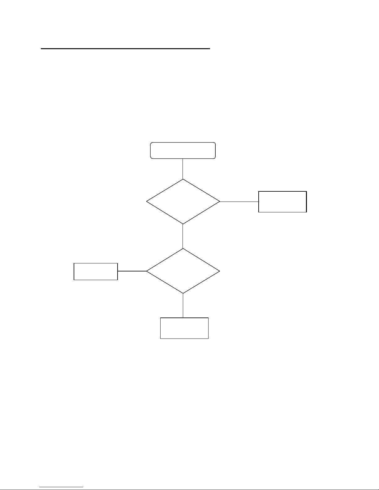
8.0 - REPAIR PROCEDURE FLOWCHART – AUDIO CIRCUIT
Without sound
Models CR20310/29411
Check IC101
C404
C404
R445/430
Q430
C440/431R432
IC490 or VCC
IC101 C409
No
IC101 pin 43
Signal.
OK ?
Yes
Models CR14300/20300
No
IC101 pin 28
Signal .
OK ?
Yes
No
IC 490 pin
14 Signal.
OK ?
Yes
No
IC 490 pin 13
signal.
OK ?
Yes
IC101 pin 43
No
Signal.
OK ?
Yes
Check: IC450 pin 6
and 47 signals.
OK ?
No
Yes Yes
Check IC 410
and around
components.
Check
R453 and R454
Connect the AV
Input signal.
OK ?
Check IC450 pin
29 signal .
No
No
Check : IC450
Pins 26 and 27.
OK ?
Yes
Replace
IC 450
Check IC
401 and Mute
24
Page 25

8.1 – REPAIR PROCEDURE – HORIZONTAL CIRCUIT
START
Check
X101 or IC101
Check :
R715, R716,
C716 and T702
Replace T701
No
No
No
Yes
IC101 pin 33
Signal.
OK ?
Yes
Q702: Collector voltage.
OK ?
Yes
Q701
Ok ?
Is there VCC
In
pins 14/39/54/56/61?
Check
Yes
C714
C715
Ok ?
No
Check the VCC in the
power supply
No
replace
Check: flyback
No
Flyback pin 1 voltage.
Ok ?
horizontal Yoke
E. H. T.
Ok ?
25
Yes
Yes
No
Yes
Check: flyback
Check: Yoke
Page 26

8.2 – REPAIR PROCEDURE FLOWCHART – POWER SUPPLY CIRCUIT- Stand by mode
,
Check : TH901
Start
No Yes
Check: C909
Voltage.OK ?
No
Yes
Check: IC901
pin 4 and 13
signals. OK ?
No
Yes Yes
Stand by
Is F901
open?
Yes
Check: TH901,
IC901 and Q901
Verificar
Check: IC901
Tensãos no
Voltage. OK?
ic901
No
No
Check:: IC 101
power and
horizontal
flowchart
Check in which
pin lacks voltage
and to correct
Check: Q901
D910 C919
Replace IC 901
26
Page 27
8.3 – REPAIR PROCEDURE FLOWCHART – TUNER
Check: R206,
IC102
TV doesn’t TUNE IN
Check:
Tuner
Pins 4 and 5 .
OK ?
No
R207, IC101 and
Fix the fault
No
Yes
Check: tuner supply
voltage.
OK ?
Yes
Replace tuner
27
Page 28

8.4 – REPAIR PROCEDURE FLOWCHART – POWER SUPPLY - MAIN CIRCUIT
TV DOESN´T
TURN ON
Check:
pins14/39/54
Fix the voltage
supply
Check: IC 101,
Q904 and R927
No
No
IC101
/56/61 (supply voltage).
OK ?
Yes
Check
Q904 signal.
OK ?
If it’s 12V, TV is in
stand by mode
No
Yes
Check:
D912 gate pin (9V).
OK ?
Yes
Check:
D912
28
Page 29

8.5 – REPAIR PROCEDURE FLOWCHART - SAP CIRCUIT
p
Check or replace
WITHOUT SAP
Check or
replace
IC101 / C404
No
Check: IC101 pin 28
signal.
OK ?
Yes
Check: IC430 pin 4
signal.
OK ?
Yes
Check: IC101 pin 8
signal.
OK ?
Yes
Check: IC430 pin 2
signal.
OK ?
No
No
No
Check or replace
Q430/ C432 / R433
R126I / C101
Check or replace
IC430/R434/IC401
IC1401/Q410/S
.
Yes
Check: IC490 pin
13 signal.
OK ?
Check or replace
C409 / IC101
29
Yes
No
Check or replace
IC490/R120/R109
Page 30

8.6 – REPAIR PROCEDURE FLOWCHART – VERTICAL CIRCUIT
Vertical closed
Check: VCC
+12 and -12
Fix the fault
IC101 pins
21 and 22
signals?
No
No
NoNo
IC601 pins 4
and 6
voltage. OK?
Yes
Yoke
Connected ?
Yes
IC601 pins 1
and 7
signals?
Check or replace
C601/602
R601/602/613/R612
Yes
Check or replace
IC101
Fix the fault
30
No
Yes
Check:
IC601
Ok ?
Yes
Check: Yoke
R606/608/609
C609 C615
Page 31

8.7 – REPAIR PROCEDURE FLOWCHART – VIDEO AND CHROME CIRCUIT
CHROME AND VIDEO
IC101
No
Check: IC101
pin 38, video pack
signal.
OK ?
Yes
Check: IC101 pin 40
(same signal pin 38).
OK ?
Yes
Check:
AV external video
Signal.
OK ?
Yes
No
Check: C301
No
Check: IC101
Check: IC101 pin
Check: IC101
X101
C105/106
31
34 signal.
OK ?
Yes
No
Fix the fault
Page 32

9 – WAVEFORMS
IC101 – pin 22 one chip 0.78Vpp
IC101 – pin 21 one chip 0.5 Vpp
5 ms
5 ms
IC601 – pin 7 Vertical 63Vpp
5 ms
IC901 – pin 13 Power 11.5Vpp
5µ s
IC901 – pin 2 Power 1.2Vpp
5µ s
32
Page 33

IC101 – pin 40 0.6Vpp
20 µ
IC101 – pin 38 one chip 1.5VPP
20µ s
IC101 – pin 33 0.95Vpp
IC101 – pin 34 one chip 5.7 Vpp
20µ s
20 µ s
33
Page 34

Q702 collector pin 100Vpp
20µ
Q701 base pin 10Vpp
20µ s
IC101 one chip – Pin 53 – B 4.5 Vpp
20 µ s
IC101 one chip – Pin 52 – G 3.8Vpp
20 µ s
34
Page 35

IC101 one chip – Pin 51 – R 4.5Vpp
20µ s
CRT Socket – Pin 6 – G-K 98Vpp
20 µ s
CRT Socket – Pin 11 – B 98Vpp
20 µ s
CRT Socket – Pin 8 – R 98Vpp
20 µ s
35
Page 36

REPLACEMENT PARTS CR14300
(See Product Safety Note on first page of this parts list)
Symbol SymbolStock StockDrawing DrawingDescription Description
CR14300
Electrical Parts
C101 T0000641 600763662000 CAP ELECT 10UF 50V
C102 T0000632 647984125004 CAP CERAM SMD 100NF 25V
X7R
C105 T0000633 6375A3159003 CAP CERAM SMD 22PF 50V
NPO
C108 T0000634 637384166002 CAP CERAM SMD 33PF 50V
NPO
C109 T0000632 647984125004 CAP CERAM SMD 100NF 25V
X7R
C110 C / P 600329971004 CAP ELECT 100UF 16V
C112 T0000632 647984125004 CAP CERAM SMD 100NF 25V
X7R
C113 C / P 600329971004 CAP ELECT 100UF 16V
C114 C / P 600329971004 CAP ELECT 100UF 16V
C115 T0000632 647984125004 CAP CERAM SMD 100NF 25V
X7R
C116 T0000632 647984125004 CAP CERAM SMD 100NF 25V
X7R
C118 T0000635 6375A3160000 CAP CERAM SMD 47PF 50V
NPO
C119 T0000635 6375A3160000 CAP CERAM SMD 47PF 50V
NPO
C201 T0000636 6490A3181006 CAP CERAM SMD 10NF 50V
X7R
C202 C / P 600329971004 CAP ELECT 100UF 16V
C203 T0000636 6490A3181006 CAP CERAM SMD 10NF 50V
X7R
C204 T0000641 600763662000 CAP ELECT 10UF 50V
C205 C / P 600463713004 CAP ELECT 47UF 25V
C206 T0000632 647984125004 CAP CERAM SMD 100NF 25V
X7R
C207 C / P 600763688000 CAP ELECT 22UF 50V
C208 T0000636 6490A3181006 CAP CERAM SMD 10NF 50V
X7R
C209 T0000632 647984125004 CAP CERAM SMD 100NF 25V
X7R
C301 T0000637 647984612002 CAP CERAM SMD 47NF 25V
X7R
C303 C / P 600329971004 CAP ELECT 100UF 16V
C304 T0000632 647984125004 CAP CERAM SMD 100NF 25V
X7R
C305 T0000632 647984125004 CAP CERAM SMD 100NF 25V
X7R
C306 T0000632 647984125004 CAP CERAM SMD 100NF 25V
X7R
C307 T0000641 600763662000 CAP ELECT 10UF 50V
C308 T0000632 647984125004 CAP CERAM SMD 100NF 25V
X7R
C311A T0000636 6490A3181006 CAP CERAM SMD 10NF 50V
X7R
C312 C / P 601079541003 CAP ELECT 2.2UF 100V
C313 T0000632 647984125004 CAP CERAM SMD 100NF 25V
X7R
C330 T0000638 6375A3163000 CAP CERAM SMD 100PF 50V
NPO
C331 T0000641 600763662000 CAP ELECT 10UF 50V
C334 C / P 600463713004 CAP ELECT 47UF 25V
C335 T0000640 6375A3167005 CAP CERAM SMD 330PF 50V
NPO
C340 T0000641 600763662000 CAP ELECT 10UF 50V
C341 T0000638 6375A3163000 CAP CERAM SMD 100PF 50V
NPO
C342 T0000635 6375A3160000 CAP CERAM SMD 47PF 50V
NPO
C350 T0000641 600763662000 CAP ELECT 10UF 50V
C401 T0000640 6375A3167005 CAP CERAM SMD 330PF 50V
NPO
C402 T0000642 6490A3177000 CAP CERAM SMD 4.7NF 50V
X7R
C403 C / P 600463713004 CAP ELECT 47UF 25V
C404 T0000642 6490A3177000 CAP CERAM SMD 4.7NF 50V
X7R
C405R T0000643 647887343002 CAP CERAM SMD 220NF 16V
X7R
C406 C / P 601078320003 CAP ELECT 1UF 100V
C408 C / P 650363842009 CAP POLYESTER 100NF 100V
C408R C / P 650363842009 CAP POLYESTER 100NF 100V
C409 T0000643 647887343002 CAP CERAM SMD 220NF 16V
X7R
C411 C / P 600363718006 CAP ELECT 470UF 16V
C414 C / P 600363718006 CAP ELECT 470UF 16V
C416R T0000636 6490A3181006 CAP CERAM SMD 10NF 50V
X7R
C417R T0000635 6375A3160000 CAP CERAM SMD 47PF 50V
NPO
C490 T0000642 6490A3177000 CAP CERAM SMD 4.7NF 50V
X7R
C491 C / P 601079541003 CAP ELECT 2.2UF 100V
C492 T0000642 6490A3177000 CAP CERAM SMD 4.7NF 50V
X7R
C493 C / P 601079541003 CAP ELECT 2.2UF 100V
C496 T0000641 600763662000 CAP ELECT 10UF 50V
C497 C / P 600329971004 CAP ELECT 100UF 16V
C498 T0000641 600763662000 CAP ELECT 10UF 50V
C501 T0000643 647887343002 CAP CERAM SMD 220NF 16V
X7R
C502 T0000650 6375A3169008 CAP CERAM SMD 560PF 50V
NPO
C601 T0000639 6490A3173004 CAP CERAM SMD 1NF 50V
X7R
C602 T0000639 6490A3173004 CAP CERAM SMD 1NF 50V
X7R
C603 T0000651 6101A2156003 CAP POLYPROPYLENE
PULSE 100NF 160V
C604 T0000632 647984125004 CAP CERAM SMD 100NF 25V
X7R
C605 T0000632 647984125004 CAP CERAM SMD 100NF 25V
X7R
C606 C / P 601079541003 CAP ELECT 2.2UF 100V
C607 C / P 600563669005 ELECT CAP - 100UF 35V
C608 T0000652 6490A3171001 CAP CERAM SMD 470PF 50V
X7R
C609 C / P 650363857006 CAP POLYESTER 220NF 100V
C / P - Common Part (Obtain through local parts store)
N / A - Not available as a service part
36
Page 37

REPLACEMENT PARTS (Continued) CR14300
(See Product Safety Note on first page of this parts list)
Symbol SymbolStock StockDrawing DrawingDescription Description
C610 T0000632 647984125004 CAP CERAM SMD 100NF 25V
X7R
C611 T0000632 647984125004 CAP CERAM SMD 100NF 25V
X7R
C612 T0000652 6490A3171001 CAP CERAM SMD 470PF 50V
X7R
C613 T0000653 6375A3165002 CAP CERAM SMD 220PF 50V
NPO
C614 T0000760 644463828006 CERAM CAP - 47NF 50V Z5V
C615 C / P 650263853000 CAP POLYESTER 22NF 63V
C616 T0000636 6490A3181006 CAP CERAM SMD 10NF 50V
X7R
C701 C / P 601078320003 CAP ELECT 1UF 100V
C702 T0000642 6490A3177000 CAP CERAM SMD 4.7NF 50V
X7R
C703 C / P 600329971004 CAP ELECT 100UF 16V
C704 T0000632 647984125004 CAP CERAM SMD 100NF 25V
X7R
C705 T0000655 6490A3174000 CAP CERAM SMD 2.2NF 50V
X7R
C706 C / P 601078320003 CAP ELECT 1UF 100V
C707 T0000643 647887343002 CAP CERAM SMD 220NF 16V
X7R
C708 C / P 600463713004 CAP ELECT 47UF 25V
C709 T0000655 6490A3174000 CAP CERAM SMD 2.2NF 50V
X7R
C710 T0000632 647984125004 CAP CERAM SMD 100NF 25V
X7R
C711 T0000641 600763662000 CAP ELECT 10UF 50V
C712 T0000656 642463826003 CAP CERAM 470PF 500V Y5P
C713 C / P 601381598009 CAP ELECT 22UF 250V
C714 T0000657 900163747006 CAP CERAM 470PF Y5R 2KV
C715 T0000761 610191608007 CAP POLYPROPYLENE
PULSE 4.7NF 1600V
C716 T0000659 650463854007 CAP POLYESTER 22NF 250V
C717 T0000762 650463866005 CAP POLYESTER 33NF 250V
C718 T0000657 900163747006 CAP CERAM 470PF Y5R 2KV
C719 T0000660 642463800004 CAP CERAM 1NF 500V Y5P
C720 T0000661 900163746000 CAP CERAM 1.50NF Y5R 2KV
C721 T0000660 642463800004 CAP CERAM 1NF 500V Y5P
C724 C / P 600463713004 CAP ELECT 47UF 25V
C725 T0000632 647984125004 CAP CERAM SMD 100NF 25V
X7R
C726 T0000632 647984125004 CAP CERAM SMD 100NF 25V
X7R
C727 C / P 650363842009 CAP POLYESTER 100NF 100V
C728 T0000763 610191609003 CAP POLYPROPYLENE
270NF 400V
C731 T0000632 647984125004 CAP CERAM SMD 100NF 25V
X7R
C801 T0000666 644263745003 CAP CERAM 4.70NF Z5U
900VAC
C802 T0000638 6375A3163000 CAP CERAM SMD 100PF 50V
NPO
C803 T0000656 642463826003 CAP CERAM 470PF 500V Y5P
C811 T0000653 6375A3165002 CAP CERAM SMD 220PF 50V
NPO
C821 T0000653 6375A3165002 CAP CERAM SMD 220PF 50V
NPO
C / P - Common Part (Obtain through local parts store)
N / A - Not available as a service part
C831 T0000653 6375A3165002 CAP CERAM SMD 220PF 50V
NPO
C902 C / P 600763733005 CAP ELECT 4.7UF 50V
C903 T0000667 900161448001 CAP CERAM 2.2NF 400VAC
C904 T0000668 610160960000 CAP POLYPROPYLENE
PULSE220NF 250VAC
C906 T0000666 644263745003 CAP CERAM 4.70NF Z5U
900VAC
C908 T0000666 644263745003 CAP CERAM 4.70NF Z5U
900VAC
C909 T0000670 642863827000 CAP CERAM 4.7NF 500V Y5U
C910 T0000764 6050A9657000 CAP ELECT 220UF 385V
C911 C / P 6003D3243008 CAP ELECT 470UF 16V LowZ
105C
C912 T0000656 642463826003 CAP CERAM 470PF 500V Y5P
C913 T0000672 6505D1087004 CAP POLYESTER 3.3NF 400V
C914 T0000674 6003D1884007 CAP ELECT 1000UF 16V HR
105C
C915 T0000673 900185374008 CAP CERAM 1NF 1KV
C916 T0000656 642463826003 CAP CERAM 470PF 500V Y5P
C917 T0000650 6375A3169008 CAP CERAM SMD 560PF 50V
NPO
C918 T0000674 6003D1884007 CAP ELECT 1000UF 16V HR
105C
C919 T0000657 900163747006 CAP CERAM 470PF Y5R 2KV
C920 T0000675 6011D1750005 CAP ELECT 100UF 160V HR
105C
C922 T0000657 900163747006 CAP CERAM 470PF Y5R 2KV
C924 C / P 650285117005 CAP POLYESTER 470NF 63V
C925 C / P 600329971004 CAP ELECT 100UF 16V
C926 T0000632 647984125004 CAP CERAM SMD 100NF 25V
X7R
C927 C / P 601079541003 CAP ELECT 2.2UF 100V
C928 T0000632 647984125004 CAP CERAM SMD 100NF 25V
X7R
C929 T0000667 900161448001 CAP CERAM 2.2NF 400VAC
C930 T0000649 6490A3178006 CAP CERAM SMD 5.6NF 50V
X7R
C931 T0000676 6375A3164006 CAP CERAM SMD 150PF 50V
NPO
C932 T0000642 6490A3177000 CAP CERAM SMD 4.7NF 50V
X7R
C933 T0000643 647887343002 CAP CERAM SMD 220NF 16V
X7R
C934 T0000655 6490A3174000 CAP CERAM SMD 2.2NF 50V
X7R
C935 C / P 600329971004 CAP ELECT 100UF 16V
C936 T0000639 6490A3173004 CAP CERAM SMD 1NF 50V
X7R
C937 T0000632 647984125004 CAP CERAM SMD 100NF 25V
X7R
C938 T0000643 647887343002 CAP CERAM SMD 220NF 16V
X7R
C939 T0000659 650463854007 CAP POLYESTER 22NF 250V
C943 C / P 6010D1383007 CAP ELECT 10UF 100V
C944 T0000643 647887343002 CAP CERAM SMD 220NF 16V
X7R
C945 T0000677 6490A3184005 CAP CERAM SMD 22NF 50V
X7R
37
Page 38

REPLACEMENT PARTS (Continued) CR14300
(See Product Safety Note on first page of this parts list)
Symbol SymbolStock StockDrawing DrawingDescription Description
C946 T0000656 642463826003 CAP CERAM 470PF 500V Y5P
CAB02 N / A 4103D0184015 CABLE 3V 2.5MM 300MM
CAB03 N / A 4119A9951018 EARTH WIRE
CM101 T0000678 7303A1145001 HITECH CONECTOR 2.50MM
CM401 T0000678 7303A1145001 HITECH CONECTOR 2.50MM
CM601 T0000680 7302A5570008 AMP CONECTOR 002V
P3.96MM
CM701 T0000681 7304A5571004 AMP CONECTOR 004V
P3.96MM
CM801 T0000680 7302A5570008 AMP CONECTOR 002V
P3.96MM
CM901 T0000682 7302A0036000 AMP CONECTOR 002V
P7.92MM
CM902 T0000680 7302A5570008 AMP CONECTOR 002V
P3.96MM
CM903 N / A 410380834019 CABLE ASSEMBLY 1V 300MM
D301 T0000683 460261728004 DIODE 75V 150MA (1N4531)
D601 T0000684 460461755001 DIODE 200V 1A (1N4004)
D602 T0000683 460261728004 DIODE 75V 150MA (1N4531)
D701 T0000685 460461757004 DIODE 400V 1A (1SR124)
D702 T0000683 460261728004 DIODE 75V 150MA (1N4531)
D703 T0000683 460261728004 DIODE 75V 150MA (1N4531)
D704 T0000683 460261728004 DIODE 75V 150MA (1N4531)
D810 T0000686 460293990006 DIODE 80V 100MA (1SS355)
D820 T0000686 460293990006 DIODE 80V 100MA (1SS355)
D830 T0000686 460293990006 DIODE 80V 100MA (1SS355)
D901 T0000765 460461758000 DIODE RECTIFIER 600V 1.2A
D902 T0000765 460461758000 DIODE RECTIFIER 600V 1.2A
D903 T0000765 460461758000 DIODE RECTIFIER 600V 1.2A
D904 T0000765 460461758000 DIODE RECTIFIER 600V 1.2A
D905 T0000683 460261728004 DIODE 75V 150MA (1N4531)
D907 T0000684 460461755001 DIODE 200V 1A (1N4004)
D908 T0000766 460493615000 DIODE RECTIFIER 200V 1.5A
D909 T0000766 460493615000 DIODE RECTIFIER 200V 1.5A
D910 T0000689 460422655000 DIODE BYV26C 600V/1A 30NS
D911 T0000767 460461750000 DIODE RECTIFIER 600V 1.1A
(RU2AM)
D912 T0000691 4630A5984009 TYRISTOR SCR BT149B/RA
(BT-149B)
D914 T0000683 460261728004 DIODE 75V 150MA (1N4531)
D915 T0000683 460261728004 DIODE 75V 150MA (1N4531)
D916 T0000686 460293990006 DIODE 80V 100MA (1SS355)
D917 T0000683 460261728004 DIODE 75V 150MA (1N4531)
D918 T0000683 460261728004 DIODE 75V 150MA (1N4531)
D919 T0000689 460422655000 DIODE BYV26C 600V/1A 30NS
F901A N / A 560463518007 FUSE HOLDER (H0462)
F901 T0000693 430461704008 FUSE RET. 3.15A 250V
FC803 N / A 4102D0182004 CABLE FLAT 3V 300MM
FC803 T0000694 7303A3489005 CONECTOR HOLDER 2.54MM
FC806 N / A 4102D0180001 CABLE FLAT 6V 300MM
FC806 T0000695 7306A4943003 CONECTOR HOLDER
IC101 T0000696 4615A4995009 IC TDA9380N1/2S
4615A4995009)
IC102 T0000697 461689406001 IC SMD M24C04MN EEPROM
IC401 T0000698 4615A5986001 IC TDA7499 AUDIO OUT
STEREO
IC490 T0000700 461116888006 IC CD4052 DUAL 4 CHAN
MUX/DEMUX
C / P - Common Part (Obtain through local parts store)
N / A - Not available as a service part
IC601 T0000768 4615A5241002 IC TDA9309 VERT OUT
IC901 T0000702 461594061009 IC TDA16846 CONT SMPS
IC902 T0000703 461562524003 IC PC-817X1 PHOTO
COUPLER (TLP621)
IC903 T0000704 461494713006 IC NJM431L ADJUSTABLE
REG
IC905 T0000705 461562589008 IC BA17809T (UPC78M09AHF)
IR101 T0000706 4331D2811007 REMOTE RECEIVER 56KHZ
JA491 T0000769 4310A9835003 JACK VERTICAL 2P
WHITE/YELLOW
JA492 T0000770 4310A9836000 JACK HORIZ 2P
YELLOW/WHITE
L102 T0000711 320184422009 COIL AXIAL 12UH 150MA
L103 T0000712 3201D5204008 COIL AXIAL 22UH 210MA
L104 T0000711 320184422009 COIL AXIAL 12UH 150MA
L201 T0000713 320161247006 COIL CHOKE 100UH 150MA
L301 T0000714 320161230006 COIL CHOKE 8.2UH 165MA
L701 T0000771 320178037000 COIL 12UH 1A
L901 T0000772 321186285009 COIL LINE FILTER - 1.7A
LD101 T0000773 460888569004 LED (BL-C9/H-31E)
MF301 T0000719 430761870005 FILTER CERAMIC 4.5MHZ
Q101 T0000720 462784592001 TRANSISTOR SMD NPN 45V
100MA (BC-847B)
Q102 T0000721 462884595000 TRANSISTOR SMD PNP 45V
100MA (BC-857B)
Q103 T0000721 462884595000 TRANSISTOR SMD PNP 45V
100MA (BC-857B)
Q201 T0000722 462062240005 TRANSISTOR 45V 500MA
NPN 160/320
Q301 T0000720 462784592001 TRANSISTOR SMD NPN 45V
100MA (BC-847B)
Q302 T0000720 462784592001 TRANSISTOR SMD NPN 45V
100MA (BC-847B)
Q330 T0000720 462784592001 TRANSISTOR SMD NPN 45V
100MA (BC-847B)
Q331 T0000720 462784592001 TRANSISTOR SMD NPN 45V
100MA (BC-847B)
Q340 T0000720 462784592001 TRANSISTOR SMD NPN 45V
100MA (BC-847B)
Q351 T0000720 462784592001 TRANSISTOR SMD NPN 45V
100MA (BC-847B)
Q401 T0000723 462784409002 TRANSISTOR SMD NPN 50V
100mA (DTC144EKA)
Q701 T0000774 462262362003 TRANSISTOR-1500V-4A-NPN-8MIN-HORIZ.OUT
(9340 250 60XXX)
Q702 T0000725 4620D5416000 TRANSISTOR NPN 150V
50MA (2SC2705-Y)
Q703 T0000721 462884595000 TRANSISTOR SMD PNP 45V
100MA (BC-857B)
Q810 T0000726 462288363007 TRANSISTOR NPN-300V
100MA (2SC3271)
Q811 T0000727 462162287001 TRANSISTOR 250V 50MA
PNP
Q820 T0000726 462288363007 TRANSISTOR NPN-300V
100MA (2SC3271)
Q821 T0000727 462162287001 TRANSISTOR 250V 50MA
PNP
Q830 T0000726 462288363007 TRANSISTOR NPN-300V
100MA (2SC3271)
38
Page 39

REPLACEMENT PARTS (Continued) CR14300
(See Product Safety Note on first page of this parts list)
Symbol SymbolStock StockDrawing DrawingDescription Description
Q831 T0000727 462162287001 TRANSISTOR 250V 50MA
PNP
Q901 T0000775 462488013006 TRANSISTOR REG FET 600V
30W
Q902 T0000729 4632A5988004 TYRISTOR TRIAC
BT138-600/B TO220
Q903 T0000722 462062240005 TRANSISTOR 45V 500MA
NPN 160/320
Q904 T0000720 462784592001 TRANSISTOR SMD NPN 45V
100MA (BC-847B)
Q905 T0000720 462784592001 TRANSISTOR SMD NPN 45V
100MA (BC-847B)
R101 N / A 6666A5296007 RES SMD 100R 5% 63MW
R102 C / P 660400487007 RES CARB 1K 5% 330MW
R103 C / P 6666A5313004 RES SMD 2.2K 5% 63MW
R104 C / P 660400488003 RES CARBON 5% 330MW
R105 C / P 660400488003 RES CARBON 5% 330MW
R107 C / P 660400510009 RES CARBON 100K 5%
330MW
R108 N / A 6666A5306009 RES SMD 560R 5% 63MW
R109 N / A 6666A5296007 RES SMD 100R 5% 63MW
R110 N / A 6666A5306009 RES SMD 560R 5% 63MW
R111 N / A 6666A5296007 RES SMD 100R 5% 63MW
R112 N / A 6666A5317000 RES SMD 4.7K 5% 63MW
R113 N / A 6666A5312008 RES SMD 1.8K 5% 63MW
R114 N / A 6666A5317000 RES SMD 4.7K 5% 63MW
R115 N / A 6666A5312008 RES SMD 1.8K 5% 63MW
R117 N / A 6666A5322002 RES SMD 10K 5% 63MW
R118 N / A 6666A5322002 RES SMD 10K 5% 63MW
R119 C / P 660400483001 RES CARBON 470R 5%
330MW
R120 C / P 660400483001 RES CARBON 470R 5%
330MW
R121 C / P 660400501000 RES CARBON 15K 5% 330MW
R122 N / A 6666A5296007 RES SMD 100R 5% 63MW
R123 N / A 6666A5296007 RES SMD 100R 5% 63MW
R126 N / A 6666A5326008 RES SMD 22K 5% 63MW
R128 N / A 6666A5322002 RES SMD 10K 5% 63MW
R129 N / A 6666A5304006 RES SMD 470R 5% 63MW
R130 N / A 6666A5322002 RES SMD 10K 5% 63MW
R131 N / A 6666A5322002 RES SMD 10K 5% 63MW
R132 C / P 660400499005 RES CARBON 10K 5% 330MW
R135 C / P 660400466000 RES CARBON 18R 5% 330MW
R201 C / P 6625D1885003 RES METAL 22K 5% 2W
R202 N / A 6666A5296007 RES SMD 100R 5% 63MW
R203 N / A 6666A5296007 RES SMD 100R 5% 63MW
R204 N / A 6666A5294004 RES SMD 82R 5% 63MW
R205 N / A 6666A5308001 RES SMD 820R 5% 63MW
R206 N / A 6666A5319002 RES SMD 6.8K 5% 63MW
R207 C / P 660400485004 RES CARBON 680R 5%
330MW
R208 N / A 6666A5318006 RES SMD 5.6K 5% 63MW
R209 N / A 6666A5322002 RES SMD 10K 5% 63MW
R301 C / P 660400487007 RES CARB 1K 5% 330MW
R302 N / A 6666A5303000 RES SMD 390R 5% 63MW
R303 N / A 6666A5283003 RES SMD 4.7R 5% 63MW
R305 N / A 6666A5290009 RES SMD 47R 5% 63MW
R306 N / A 6666A5296007 RES SMD 100R 5% 63MW
R307 N / A 6666A5300000 RES SMD 220R 5% 63MW
R308 N / A 6666A5309008 RES SMD 1K 5% 63MW
R309 N / A 6666A5297003 RES SMD 120R 5% 63MW
R310 N / A 6666A5301007 RES SMD 270R 5% 63MW
R311 N / A 6666A5297003 RES SMD 120R 5% 63MW
R330 N / A 6666A5293008 RES SMD 75R 5% 63MW
R331 C / P 660400475009 RES CARBON 100R 5%
330MW
R332 N / A 6666A5317000 RES SMD 4.7K 5% 63MW
R333 N / A 6666A5315007 RES SMD 3.3K 5% 63MW
R334 N / A 6666A5300000 RES SMD 220R 5% 63MW
R335 N / A 6666A5328000 RES SMD 33K 5% 63MW
R336 N / A 6666A5335006 RES SMD 100K 5% 63MW
R340 N / A 6666A5293008 RES SMD 75R 5% 63MW
R341 C / P 660400475009 RES CARBON 100R 5%
330MW
R341 C / P 660400475009 RES CARBON 100R 5%
330MW
R341 C / P 660400475009 RES CARBON 100R 5%
330MW
R342 N / A 6666A5315007 RES SMD 3.3K 5% 63MW
R343 N / A 6666A5317000 RES SMD 4.7K 5% 63MW
R345 N / A 6666A5335006 RES SMD 100K 5% 63MW
R345R N / A 6666A5335006 RES SMD 100K 5% 63MW
R347 C / P 660400471003 RES CARBON 47R 5% 330MW
R354 N / A 6666A5328000 RES SMD 33K 5% 63MW
R356 N / A 6666A5335006 RES SMD 100K 5% 63MW
R356R N / A 6666A5335006 RES SMD 100K 5% 63MW
R357 N / A 6666A5335006 RES SMD 100K 5% 63MW
R358 N / A 6666A5335006 RES SMD 100K 5% 63MW
R401 N / A 6666A5316003 RES SMD 3.9K 5% 63MW
R403 C / P 660400475009 RES CARBON 100R 5%
330MW
R403 C / P 660400475009 RES CARBON 100R 5%
330MW
R403 C / P 660400475009 RES CARBON 100R 5%
330MW
R404 N / A 6666A5321006 RES SMD 8.2K 5% 63MW
R404R N / A 6666A5321006 RES SMD 8.2K 5% 63MW
R405 N / A 6666A5306009 RES SMD 560R 5% 63MW
R405R N / A 6666A5306009 RES SMD 560R 5% 63MW
R406R C / P 666464075001 RES CARBON/METAL 4.7R
5% 0.5W
R407 N / A 6666A5324005 RES SMD 15K 5% 63MW
R408 T0000776 6628D1439005 RES METAL 8.20R 5% 2W
R409 T0000776 6628D1439005 RES METAL 8.20R 5% 2W
R410 N / A 6666A5296007 RES SMD 100R 5% 63MW
R453 C / P 660400475009 RES CARBON 100R 5%
330MW
R490 N / A 6666A5322002 RES SMD 10K 5% 63MW
R491 C / P 660400487007 RES CARB 1K 5% 330MW
R492 N / A 6666A5322002 RES SMD 10K 5% 63MW
R493 C / P 660400487007 RES CARB 1K 5% 330MW
R496 N / A 6666A5312008 RES SMD 1.8K 5% 63MW
R497 N / A 6666A5312008 RES SMD 1.8K 5% 63MW
R498 C / P 660400490008 RES CARBON 1.8K 5%
330MW
R504 C / P 660400499005 RES CARBON 10K 5% 330MW
C / P - Common Part (Obtain through local parts store)
N / A - Not available as a service part
39
Page 40

REPLACEMENT PARTS (Continued) CR14300
(See Product Safety Note on first page of this parts list)
Symbol SymbolStock StockDrawing DrawingDescription Description
R505 C / P 660400475009 RES CARBON 100R 5%
330MW
R506 C / P 660400475009 RES CARBON 100R 5%
330MW
R507 C / P 660400475009 RES CARBON 100R 5%
330MW
R601 C / P 660400479004 RES CARBON 220R 5%
330MW
R602 C / P 660400479004 RES CARBON 220R 5%
330MW
R603 N / A 6667A5365000 RES SMD 39K 1% 63MW
R604 N / A 6666A5325001 RES SMD 18K 5% 0.063W
R605 C / P 660400499005 RES CARBON 10K 5% 330MW
R606 C / P 660400485004 RES CARBON 680R 5%
330MW
R607 N / A 6666A5310005 RES SMD 5% 63MW
R608 C / P 666400536008 RES CARBON/METAL 2.2R
5% 0.5W
R609 C / P 666464031004 RES CARBON/METAL 3.3R
5% 0.5W
R610 C / P 662377519000 RES METAL 1.5R 5% 1W
R611 N / A 6666A5310005 RES SMD 5% 63MW
R612 C / P 660400487007 RES CARB 1K 5% 330MW
R613 C / P 660400487007 RES CARB 1K 5% 330MW
R701 N / A 6666A5324005 RES SMD 15K 5% 63MW
R702 N / A 6666A5326008 RES SMD 22K 5% 63MW
R703 N / A 6666A5322002 RES SMD 10K 5% 63MW
R704 C / P 660400495000 RES CARBON 4.7K 5%
330MW
R705 N / A 6666A5300000 RES SMD 220R 5% 63MW
R706 C / P 660400491004 RES CARBON 2.2K 5%
330MW
R707 C / P 660400504009 RES CARBON 27K 5% 330MW
R708 C / P 660400484008 RES CARBON 560R 5%
330MW
R708 T0000711 320184422009 COIL AXIAL 12UH 150MA
R710 N / A 6666A5338005 RES SMD 220K 5% 63MW
R712 C / P 660400499005 RES CARBON 10K 5% 330MW
R713 N / A 6666A5312008 RES SMD 1.8K 5% 63MW
R714 T0000731 663588638006 RES FUSE 4.7R 5% 0.5W
R715 T0000777 6628D2868004 RES METAL 3.3K 5% 3W
R716 T0000778 6628A8908000 RES METAL 1.2K 5% 3W
R717 C / P 666464051005 RES CARBON/METAL 3.9R
5% 0.5W
R718 N / A 660400496006 RES CARBON 5.6K 5%
330MW
R719 T0000732 6645D2210004 RES WIRE 3.3R 5% 5W
R721 N / A 6666A5284000 RES SMD - 10R 5% 63MW
R722 N / A 6666A5326008 RES SMD 22K 5% 63MW
R723 N / A 6666A5322002 RES SMD 10K 5% 63MW
R724 C / P 660400499005 RES CARBON 10K 5% 330MW
R725 C / P 662263904004 RES METAL 100K 5% 0.5W
R727 C / P 6666A5314000 RES SMD 2.7K 5% 63MW
R750 T0000777 6628D2868004 RES METAL 3.3K 5% 3W
R811 C / P 6666A5302003 RES SMD 330R 5% 63MW
R812 C / P 6666A5313004 RES SMD 2.2K 5% 63MW
R813 C / P 662890269004 RES METAL 10K 5% 2W
R814 C / P 660400490008 RES CARBON 1.8K 5%
330MW
C / P - Common Part (Obtain through local parts store)
N / A - Not available as a service part
R815A C / P 660985299006 RES CARBON 1.5K 10% 0.5W
R821 C / P 6666A5302003 RES SMD 330R 5% 63MW
R822 C / P 6666A5313004 RES SMD 2.2K 5% 63MW
R823 C / P 662890269004 RES METAL 10K 5% 2W
R824 C / P 660400490008 RES CARBON 1.8K 5%
330MW
R825 C / P 660985299006 RES CARBON 1.5K 10% 0.5W
R831 C / P 6666A5302003 RES SMD 330R 5% 63MW
R832 C / P 6666A5313004 RES SMD 2.2K 5% 63MW
R833 C / P 662890269004 RES METAL 10K 5% 2W
R834 C / P 660400490008 RES CARBON 1.8K 5%
330MW
R835A C / P 660985299006 RES CARBON 1.5K 10% 0.5W
R902 C / P 6628D1892009 RES METAL 18K 5% 3W
R903 N / A 6666A5290009 RES SMD 47R 5% 63MW
R906 N / A 6666A5334000 RES SMD 82K 5% 63MW
R907 T0000733 6635A4368008 RES FUSE 0.47R 5% 0.5W
R908 T0000733 6635A4368008 RES FUSE 0.47R 5% 0.5W
R909 C / P 6664A9708006 RES CARBON/METAL 390K
5% 0.5W
R910 T0000733 6635A4368008 RES FUSE 0.47R 5% 0.5W
R911 C / P 6620D1815001 RES METAL 2.2M 1% 0.5W
R912 T0000733 6635A4368008 RES FUSE 0.47R 5% 0.5W
R913 N / A 6666A5328000 RES SMD 33K 5% 63MW
R914 C / P 660463994003 RES CARBON 22R 5% 330MW
R915 T0000734 666400548006 RES CARB/MET 22R 5% 0.5W
R917 T0000735 6634A9755000 RES FUSE 2.2K 5% 330MW
R918 C / P 660400472000 RES CARBON 56R 5% 330MW
R919 C / P 661999970007 RES METAL 120K 1% 400MW
R920 N / A 6666A5309008 RES SMD 1K 5% 63MW
R921 C / P 6619D1939009 RES METAL 20K 1% 400MW
R923 C / P 660400484008 RES CARBON 560R 5%
330MW
R924 C / P 660400512001 RES CARBON 150K 5%
330MW
R925 C / P 662763911000 RES METAL 10M 5% 0.5W
R926 C / P 660400487007 RES CARB 1K 5% 330MW
R927 C / P 660400499005 RES CARBON 10K 5% 330MW
R928 N / A 6666A5322002 RES SMD 10K 5% 63MW
R929 C / P 6666A5313004 RES SMD 2.2K 5% 63MW
R930 C / P 662280514006 RES METAL 470R 5% 0.5W
R931 N / A 6666A5328000 RES SMD 33K 5% 63MW
R932 N / A 6666A5309008 RES SMD 1K 5% 63MW
R933 C / P 660400501000 RES CARBON 15K 5% 330MW
R934 N / A 6666A5319002 RES SMD 6.8K 5% 63MW
R935 N / A 6666A5322002 RES SMD 10K 5% 63MW
R936 N / A 6666A5307005 RES SMD 680R 5% 63MW
R937 N / A 6667D1088000 RES SMD 3K 1% 63MW
R939 N / A 6666A5307005 RES SMD 680R 5% 63MW
R940 C / P 666495473009 RES CARBON/METAL 5%
0.5W
R941 N / A 6666A5312008 RES SMD 1.8K 5% 63MW
R942 C / P 660400499005 RES CARBON 10K 5% 330MW
R943 C / P 6623D5217001 RES METAL 6.8K 5% 1W
R944 N / A 6666A5335006 RES SMD 100K 5% 63MW
RJ01 T0000662 6666A5277004 RES SMD 0R 5% 63MW
RJ102 T0000662 6666A5277004 RES SMD 0R 5% 63MW
SF201 T0000736 432461879002 FILTER SAW
40
Page 41

REPLACEMENT PARTS (Continued) CR14300
(See Product Safety Note on first page of this parts list)
Symbol SymbolStock StockDrawing DrawingDescription Description
SW101 T0000739 4301A5983002 SWITCH TACT
SW102 T0000739 4301A5983002 SWITCH TACT
SW103 T0000739 4301A5983002 SWITCH TACT
SW104 T0000739 4301A5983002 SWITCH TACT
SW105 T0000739 4301A5983002 SWITCH TACT
SW106 T0000739 4301A5983002 SWITCH TACT
T701 T0000781 321090815041 TRANSFORMER FLYBACK
T702 T0000741 320984559012 DRIVER TRANSFORMER
T901 T0000782 3208D0149019 TRANSFORMER SWITCHING
TH901 T0000783 668361453005 THERMISTOR-PTC 18R
TH902 T0000744 668394919003 THERMISTOR NTC 4.7R
TU201 T0000745 431299421003 TUNER (5V) (UVE25-AW52D)
X101 T0000746 4306A4722002 CRYSTAL 12.00MHZ 20PF
ZD101 T0000748 460761767000 DIODE ZENER 3.9V 0.5W 5%
ZD201 T0000749 460761775002 DIODE ZENER 5.6V 0.5W 2%
ZD202 T0000750 460761805009 DIODE ZENER 33V 0.5W 2%
ZD501 T0000751 460761783005 DIODE ZENER 8.2V 0.5W 5%
ZD502 T0000751 460761783005 DIODE ZENER 8.2V 0.5W 5%
ZD503 T0000751 460761783005 DIODE ZENER 8.2V 0.5W 5%
ZD701 T0000751 460761783005 DIODE ZENER 8.2V 0.5W 5%
ZD702 T0000751 460761783005 DIODE ZENER 8.2V 0.5W 5%
ZD801 T0000751 460761783005 DIODE ZENER 8.2V 0.5W 5%
ZD902 T0000748 460761767000 DIODE ZENER 3.9V 0.5W 5%
ZD903 T0000752 460761777005 DIODE ZENER 6.2V 0.5W 2%
ZD904 T0000753 460761792004 DIODE ZENER 12V 0.5W 5%
ZD905 T0000754 460761771007 DIODE ZENER 5.1V 0.5W 5%
ZD906 T0000753 460761792004 DIODE ZENER 12V 0.5W 5%
ZD907 T0000755 4607A9793005 DIODE ZENER 43V 0.5W 5%
ZD908 T0000756 4607A9794001 DIODE ZENER 47V 0.5W 5%
SPKR01 T0000779 360186284002 SPEAKER 16R 4X7CM 5W
SQ801 T0000780 432285242004 CRT SOCKET (MINI NECK
SOLDERLESS)
STRP01 N / A 540162960008 DEGAUSS COIL STRAP
STRP02 N / A 217162708007 PLASTIC STRAP
SUPP01 N / A 540162961004 SUPPORT TO DEGAUSS
COIL
Included Accessories
ADPT01 T0000757 4315D5086001 ADAPTER PLUG
CYLINDRICAL TO FLAT
ANT1 T0000758 431864464008 TELESCOPIC ANTENNA
BATT01 C / P 4313D7395000 BATTERY SET (AAA) RCA
(XX50853-970)
REM01 240959 4317D2704009 REMOTE CONTROL
(XX15207-620)
Instrument/Cabinet Parts
BACK01 N / A 5401D2728020 CR14300 BACK COVER
BOB1 T0000759 3205A9948018 14" DEGAUSS COIL
BUTT01 N / A 5401A8987019 FUNCTION BUTTON
CRT01 N / A 3414D4835003 CR14300 CRT
(A34EJM34X045HR)
CABN01 N / A 2030D2725020 CR14300 PREPARED
CABINET SET
CABN02 N / A 5401A8985024 CABINET
CABO1 N / A 4103A4392003 POWER CORD
IC601A N / A 2030D0720019 HEAT SINK VERT SET
IC601B N / A 212160746009 WASHER PR 3.2X5.5X0.8
IC601C N / A 210160707003 SCREW M3X8 PAN
IC601D N / A 211160753005 NUT M3 CR
IC905A N / A 2030D0956016 20X40 HEAT SET
IC905B N / A 212160746009 WASHER PR 3.2X5.5X0.8
IC905C N / A 210160707003 SCREW M3X8 PAN
IC905D N / A 211160753005 NUT M3 CR
PCB01 N / A 5502A6183010 CP02R0 MAIN BOARD
PCB02 N / A 5502A6184016 CP02R0 CRT PCB
Q901A N / A 2030D0721015 HEAT SINK REG POWER
SOURCE SET
Q901B N / A 212160746009 WASHER PR 3.2X5.5X0.8
Q901C N / A 210160708000 SCREW M3X12 PAN
DIFF01 N / A 5401A8984010 DIFUSOR
Q901D N / A 211160753005 NUT M3 CR
SCRW01 N / A 210386100009 SCREW 6.35X22 PAN
C / P - Common Part (Obtain through local parts store)
N / A - Not available as a service part
41
Page 42

REPLACEMENT PARTS (Continued) CR20300
(See Product Safety Note on first page of this parts list)
Symbol SymbolStock StockDrawing DrawingDescription Description
CR20300
Electrical Parts
C101 T0000641 600763662000 CAP ELECT 10UF 50V
C102 T0000632 647984125004 CAP CERAM SMD 100NF 25V
X7R
C105 T0000633 6375A3159003 CAP CERAM SMD 22PF 50V
NPO
C108 T0000634 637384166002 CAP CERAM SMD 33PF 50V
NPO
C109 T0000632 647984125004 CAP CERAM SMD 100NF 25V
X7R
C110 C / P 600329971004 CAP ELECT 100UF 16V
C112 T0000632 647984125004 CAP CERAM SMD 100NF 25V
X7R
C113 C / P 600329971004 CAP ELECT 100UF 16V
C114 C / P 600329971004 CAP ELECT 100UF 16V
C115 T0000632 647984125004 CAP CERAM SMD 100NF 25V
X7R
C116 T0000632 647984125004 CAP CERAM SMD 100NF 25V
X7R
C118 T0000635 6375A3160000 CAP CERAM SMD 47PF 50V
NPO
C119 T0000635 6375A3160000 CAP CERAM SMD 47PF 50V
NPO
C201 T0000636 6490A3181006 CAP CERAM SMD 10NF 50V
X7R
C202 C / P 600329971004 CAP ELECT 100UF 16V
C203 T0000636 6490A3181006 CAP CERAM SMD 10NF 50V
X7R
C204 T0000641 600763662000 CAP ELECT 10UF 50V
C205 C / P 600463713004 CAP ELECT 47UF 25V
C206 T0000632 647984125004 CAP CERAM SMD 100NF 25V
X7R
C207 C / P 600763688000 CAP ELECT 22UF 50V
C208 T0000636 6490A3181006 CAP CERAM SMD 10NF 50V
X7R
C209 T0000632 647984125004 CAP CERAM SMD 100NF 25V
X7R
C301 T0000637 647984612002 CAP CERAM SMD 47NF 25V
X7R
C303 C / P 600329971004 CAP ELECT 100UF 16V
C304 T0000632 647984125004 CAP CERAM SMD 100NF 25V
X7R
C305 T0000632 647984125004 CAP CERAM SMD 100NF 25V
X7R
C306 T0000632 647984125004 CAP CERAM SMD 100NF 25V
X7R
C307 T0000641 600763662000 CAP ELECT 10UF 50V
C308 T0000632 647984125004 CAP CERAM SMD 100NF 25V
X7R
C311A T0000636 6490A3181006 CAP CERAM SMD 10NF 50V
X7R
C312 C / P 601079541003 CAP ELECT 2.2UF 100V
C313 T0000632 647984125004 CAP CERAM SMD 100NF 25V
X7R
C330 T0000638 6375A3163000 CAP CERAM SMD 100PF 50V
NPO
C / P - Common Part (Obtain through local parts store)
N / A - Not available as a service part
C331 T0000641 600763662000 CAP ELECT 10UF 50V
C334 C / P 600463713004 CAP ELECT 47UF 25V
C335 T0000640 6375A3167005 CAP CERAM SMD 330PF 50V
NPO
C340 T0000641 600763662000 CAP ELECT 10UF 50V
C341 T0000638 6375A3163000 CAP CERAM SMD 100PF 50V
NPO
C342 T0000635 6375A3160000 CAP CERAM SMD 47PF 50V
NPO
C350 T0000641 600763662000 CAP ELECT 10UF 50V
C401 T0000640 6375A3167005 CAP CERAM SMD 330PF 50V
NPO
C402 T0000642 6490A3177000 CAP CERAM SMD 4.7NF 50V
X7R
C403 C / P 600463713004 CAP ELECT 47UF 25V
C404 T0000642 6490A3177000 CAP CERAM SMD 4.7NF 50V
X7R
C405R T0000643 647887343002 CAP CERAM SMD 220NF 16V
X7R
C406 C / P 601078320003 CAP ELECT 1UF 100V
C408R C / P 650363842009 CAP POLYESTER 100NF 100V
C409 T0000643 647887343002 CAP CERAM SMD 220NF 16V
X7R
C411 C / P 600363718006 CAP ELECT 470UF 16V
C414 C / P 600363718006 CAP ELECT 470UF 16V
C416R T0000636 6490A3181006 CAP CERAM SMD 10NF 50V
X7R
C417R T0000635 6375A3160000 CAP CERAM SMD 47PF 50V
NPO
C490 T0000642 6490A3177000 CAP CERAM SMD 4.7NF 50V
X7R
C491 C / P 601079541003 CAP ELECT 2.2UF 100V
C492 T0000642 6490A3177000 CAP CERAM SMD 4.7NF 50V
X7R
C493 C / P 601079541003 CAP ELECT 2.2UF 100V
C496 T0000641 600763662000 CAP ELECT 10UF 50V
C497 C / P 600329971004 CAP ELECT 100UF 16V
C498 T0000641 600763662000 CAP ELECT 10UF 50V
C501 T0000643 647887343002 CAP CERAM SMD 220NF 16V
X7R
C502 T0000650 6375A3169008 CAP CERAM SMD 560PF 50V
NPO
C601 T0000639 6490A3173004 CAP CERAM SMD 1NF 50V
X7R
C602 T0000639 6490A3173004 CAP CERAM SMD 1NF 50V
X7R
C603 T0000651 6101A2156003 CAP POLYPROPYLENE
PULSE 100NF 160V
C604 T0000632 647984125004 CAP CERAM SMD 100NF 25V
X7R
C605 T0000632 647984125004 CAP CERAM SMD 100NF 25V
X7R
C606 C / P 601079541003 CAP ELECT 2.2UF 100V
C607 C / P 600563669005 ELECT CAP - 100UF 35V
C608 T0000652 6490A3171001 CAP CERAM SMD 470PF 50V
X7R
C609 C / P 650363857006 CAP POLYESTER 220NF 100V
C610 T0000632 647984125004 CAP CERAM SMD 100NF 25V
X7R
42
Page 43

REPLACEMENT PARTS (Continued) CR20300
(See Product Safety Note on first page of this parts list)
Symbol SymbolStock StockDrawing DrawingDescription Description
C611 T0000632 647984125004 CAP CERAM SMD 100NF 25V
X7R
C612 T0000652 6490A3171001 CAP CERAM SMD 470PF 50V
X7R
C613 T0000653 6375A3165002 CAP CERAM SMD 220PF 50V
NPO
C614 T0000760 644463828006 CERAM CAP - 47NF 50V Z5V
C615 C / P 650263853000 CAP POLYESTER 22NF 63V
C616 T0000636 6490A3181006 CAP CERAM SMD 10NF 50V
X7R
C701 C / P 601078320003 CAP ELECT 1UF 100V
C702 T0000642 6490A3177000 CAP CERAM SMD 4.7NF 50V
X7R
C703 C / P 600329971004 CAP ELECT 100UF 16V
C704 T0000632 647984125004 CAP CERAM SMD 100NF 25V
X7R
C705 T0000655 6490A3174000 CAP CERAM SMD 2.2NF 50V
X7R
C706 C / P 601078320003 CAP ELECT 1UF 100V
C707 T0000643 647887343002 CAP CERAM SMD 220NF 16V
X7R
C708 C / P 600463713004 CAP ELECT 47UF 25V
C709 T0000655 6490A3174000 CAP CERAM SMD 2.2NF 50V
X7R
C710 T0000632 647984125004 CAP CERAM SMD 100NF 25V
X7R
C711 T0000641 600763662000 CAP ELECT 10UF 50V
C712 T0000656 642463826003 CAP CERAM 470PF 500V Y5P
C713 C / P 601381598009 CAP ELECT 22UF 250V
C714 T0000657 900163747006 CAP CERAM 470PF Y5R 2KV
C715 T0000658 610160966009 CAP POLYPROPYLENE
PULSE 6.80NF 1600V
C715 T0000761 610191608007 CAP POLYPROPYLENE
PULSE 4.7NF 1600V
C716 T0000659 650463854007 CAP POLYESTER 22NF 250V
C717 T0000762 650463866005 CAP POLYESTER 33NF 250V
C718 T0000657 900163747006 CAP CERAM 470PF Y5R 2KV
C719 T0000660 642463800004 CAP CERAM 1NF 500V Y5P
C720 T0000661 900163746000 CAP CERAM 1.50NF Y5R 2KV
C721 T0000660 642463800004 CAP CERAM 1NF 500V Y5P
C724 C / P 600463713004 CAP ELECT 47UF 25V
C725 T0000632 647984125004 CAP CERAM SMD 100NF 25V
X7R
C726 T0000632 647984125004 CAP CERAM SMD 100NF 25V
X7R
C727 C / P 650363842009 CAP POLYESTER 100NF 100V
C728 T0000785 610160965002 PULSE POLYPROPYLENE
CAP - 470,00NF-0250V
C731 T0000632 647984125004 CAP CERAM SMD 100NF 25V
X7R
C801 T0000666 644263745003 CAP CERAM 4.70NF Z5U
900VAC
C802 T0000638 6375A3163000 CAP CERAM SMD 100PF 50V
NPO
C803 T0000656 642463826003 CAP CERAM 470PF 500V Y5P
C811 T0000653 6375A3165002 CAP CERAM SMD 220PF 50V
NPO
C821 T0000653 6375A3165002 CAP CERAM SMD 220PF 50V
NPO
C / P - Common Part (Obtain through local parts store)
N / A - Not available as a service part
C831 T0000653 6375A3165002 CAP CERAM SMD 220PF 50V
NPO
C902 C / P 600763733005 CAP ELECT 4.7UF 50V
C903 T0000667 900161448001 CAP CERAM 2.2NF 400VAC
C904 T0000668 610160960000 CAP POLYPROPYLENE
PULSE220NF 250VAC
C906 T0000666 644263745003 CAP CERAM 4.70NF Z5U
900VAC
C907 T0000669 6375A3170005 CAP CERAM SMD 680PF 50V
NPO
C908 T0000666 644263745003 CAP CERAM 4.70NF Z5U
900VAC
C909 T0000670 642863827000 CAP CERAM 4.7NF 500V Y5U
C910 T0000764 6050A9657000 CAP ELECT 220UF 385V
C911 C / P 6003D3243008 CAP ELECT 470UF 16V LowZ
105C
C912 T0000656 642463826003 CAP CERAM 470PF 500V Y5P
C913 T0000672 6505D1087004 CAP POLYESTER 3.3NF 400V
C914 T0000674 6003D1884007 CAP ELECT 1000UF 16V HR
105C
C915 T0000673 900185374008 CAP CERAM 1NF 1KV
C916 T0000656 642463826003 CAP CERAM 470PF 500V Y5P
C917 T0000669 6375A3170005 CAP CERAM SMD 680PF 50V
NPO
C918 T0000674 6003D1884007 CAP ELECT 1000UF 16V HR
105C
C919 T0000657 900163747006 CAP CERAM 470PF Y5R 2KV
C920 T0000675 6011D1750005 CAP ELECT 100UF 160V HR
105C
C922 T0000657 900163747006 CAP CERAM 470PF Y5R 2KV
C924 C / P 650285117005 CAP POLYESTER 470NF 63V
C925 C / P 600329971004 CAP ELECT 100UF 16V
C926 T0000632 647984125004 CAP CERAM SMD 100NF 25V
X7R
C927 C / P 601079541003 CAP ELECT 2.2UF 100V
C928 T0000632 647984125004 CAP CERAM SMD 100NF 25V
X7R
C929 T0000667 900161448001 CAP CERAM 2.2NF 400VAC
C930 T0000649 6490A3178006 CAP CERAM SMD 5.6NF 50V
X7R
C931 T0000676 6375A3164006 CAP CERAM SMD 150PF 50V
NPO
C932 T0000642 6490A3177000 CAP CERAM SMD 4.7NF 50V
X7R
C933 T0000643 647887343002 CAP CERAM SMD 220NF 16V
X7R
C934 T0000655 6490A3174000 CAP CERAM SMD 2.2NF 50V
X7R
C935 C / P 600329971004 CAP ELECT 100UF 16V
C936 T0000639 6490A3173004 CAP CERAM SMD 1NF 50V
X7R
C937 T0000632 647984125004 CAP CERAM SMD 100NF 25V
X7R
C938 T0000643 647887343002 CAP CERAM SMD 220NF 16V
X7R
C939 T0000659 650463854007 CAP POLYESTER 22NF 250V
C943 C / P 6010D1383007 CAP ELECT 10UF 100V
C944 T0000643 647887343002 CAP CERAM SMD 220NF 16V
X7R
43
Page 44

REPLACEMENT PARTS (Continued) CR20300
(See Product Safety Note on first page of this parts list)
Symbol SymbolStock StockDrawing DrawingDescription Description
C945 T0000677 6490A3184005 CAP CERAM SMD 22NF 50V
X7R
C946 T0000656 642463826003 CAP CERAM 470PF 500V Y5P
CAB02 N / A 4103D0184015 CABLE 3V 2.5MM 300MM
CAB03 N / A 4119A9952014 EARTH WIRE
CM101 T0000678 7303A1145001 HITECH CONECTOR 2.50MM
CM401 T0000678 7303A1145001 HITECH CONECTOR 2.50MM
CM601 T0000680 7302A5570008 AMP CONECTOR 002V
P3.96MM
CM701 T0000681 7304A5571004 AMP CONECTOR 004V
P3.96MM
CM801 T0000680 7302A5570008 AMP CONECTOR 002V
P3.96MM
CM852 N / A 4103A5096010 CABLE ASSEMBLY 1V 400MM
CM901 T0000682 7302A0036000 AMP CONECTOR 002V
P7.92MM
CM902 T0000680 7302A5570008 AMP CONECTOR 002V
P3.96MM
CM903 N / A 410380834019 CABLE ASSEMBLY 1V 300MM
D301 T0000683 460261728004 DIODE 75V 150MA (1N4531)
D601 T0000684 460461755001 DIODE 200V 1A (1N4004)
D602 T0000683 460261728004 DIODE 75V 150MA (1N4531)
D701 T0000685 460461757004 DIODE 400V 1A (1SR124)
D702 T0000683 460261728004 DIODE 75V 150MA (1N4531)
D703 T0000683 460261728004 DIODE 75V 150MA (1N4531)
D704 T0000683 460261728004 DIODE 75V 150MA (1N4531)
D810 T0000686 460293990006 DIODE 80V 100MA (1SS355)
D820 T0000686 460293990006 DIODE 80V 100MA (1SS355)
D830 T0000686 460293990006 DIODE 80V 100MA (1SS355)
D901 T0000765 460461758000 DIODE RECTIFIER 600V 1.2A
D902 T0000765 460461758000 DIODE RECTIFIER 600V 1.2A
D903 T0000765 460461758000 DIODE RECTIFIER 600V 1.2A
D904 T0000765 460461758000 DIODE RECTIFIER 600V 1.2A
D905 T0000683 460261728004 DIODE 75V 150MA (1N4531)
D907 T0000684 460461755001 DIODE 200V 1A (1N4004)
D908 T0000766 460493615000 DIODE RECTIFIER 200V 1.5A
D909 T0000766 460493615000 DIODE RECTIFIER 200V 1.5A
D910 T0000689 460422655000 DIODE BYV26C 600V/1A 30NS
D911 T0000767 460461750000 DIODE RECTIFIER 600V 1.1A
(RU2AM)
D912 T0000691 4630A5984009 TYRISTOR SCR BT149B/RA
(BT-149B)
D914 T0000683 460261728004 DIODE 75V 150MA (1N4531)
D915 T0000683 460261728004 DIODE 75V 150MA (1N4531)
D916 T0000686 460293990006 DIODE 80V 100MA (1SS355)
D917 T0000683 460261728004 DIODE 75V 150MA (1N4531)
D918 T0000683 460261728004 DIODE 75V 150MA (1N4531)
D919 T0000689 460422655000 DIODE BYV26C 600V/1A 30NS
F901 T0000693 430461704008 FUSE RET. 3.15A 250V
F901A N / A 560463518007 FUSE HOLDER (H0462)
FC803 N / A 4102D0182004 CABLE FLAT 3V 300MM
FC803 T0000694 7303A3489005 CONECTOR HOLDER 2.54MM
FC806 N / A 4102D0179004 CABLE FLAT 6V 380MM
FC806 T0000695 7306A4943003 CONECTOR HOLDER
IC101 T0000696 4615A4995009 IC TDA9380N1/2S
4615A4995009)
IC102 T0000697 461689406001 IC SMD M24C04MN EEPROM
IC401 T0000698 4615A5986001 IC TDA7499 AUDIO OUT
STEREO
C / P - Common Part (Obtain through local parts store)
N / A - Not available as a service part
IC490 T0000700 461116888006 IC CD4052 DUAL 4 CHAN
MUX/DEMUX
IC601 T0000768 4615A5241002 IC TDA9309 VERT OUT
IC901 T0000702 461594061009 IC TDA16846 CONT SMPS
IC902 T0000703 461562524003 IC PC-817X1 PHOTO
COUPLER (TLP621)
IC903 T0000704 461494713006 IC NJM431L ADJUSTABLE
REG
IC905 T0000705 461562589008 IC BA17809T (UPC78M09AHF)
IR101 T0000706 4331D2811007 REMOTE RECEIVER 56KHZ
JA491 T0000769 4310A9835003 JACK VERTICAL 2P
WHITE/YELLOW
JA492 T0000770 4310A9836000 JACK HORIZ 2P
YELLOW/WHITE
L102 T0000711 320184422009 COIL AXIAL 12UH 150MA
L103 T0000712 3201D5204008 COIL AXIAL 22UH 210MA
L104 T0000711 320184422009 COIL AXIAL 12UH 150MA
L201 T0000713 320161247006 COIL CHOKE 100UH 150MA
L301 T0000714 320161230006 COIL CHOKE 8.2UH 165MA
L701 T0000771 320178037000 COIL 12UH 1A
L901 T0000772 321186285009 COIL LINE FILTER 1.7A
LD101 T0000773 460888569004 LED (BL-C9/H-31E)
MF301 T0000719 430761870005 FILTER, CERAMIC 4.5MHZ
Q101 T0000720 462784592001 TRANSISTOR SMD NPN 45V
100MA (BC-847B)
Q102 T0000721 462884595000 TRANSISTOR SMD PNP 45V
100MA (BC-857B)
Q103 T0000721 462884595000 TRANSISTOR SMD PNP 45V
100MA (BC-857B)
Q201 T0000722 462062240005 TRANSISTOR 45V 500MA
NPN 160/320
Q301 T0000720 462784592001 TRANSISTOR SMD NPN 45V
100MA (BC-847B)
Q302 T0000720 462784592001 TRANSISTOR SMD NPN 45V
100MA (BC-847B)
Q330 T0000720 462784592001 TRANSISTOR SMD NPN 45V
100MA (BC-847B)
Q331 T0000720 462784592001 TRANSISTOR SMD NPN 45V
100MA (BC-847B)
Q340 T0000720 462784592001 TRANSISTOR SMD NPN 45V
100MA (BC-847B)
Q351 T0000720 462784592001 TRANSISTOR SMD NPN 45V
100MA (BC-847B)
Q401 T0000723 462784409002 TRANSISTOR SMD NPN 50V
100mA (DTC144EKA)
Q701 T0000774 462262362003 TRANSISTOR-1500V-4A-NPN-8MIN-HORIZ.OUT
(9340 250 60XXX)
Q702 T0000725 4620D5416000 TRANSISTOR NPN 150V
50MA (2SC2705-Y)
Q703 T0000721 462884595000 TRANSISTOR SMD PNP 45V
100MA (BC-857B)
Q810 T0000726 462288363007 TRANSISTOR NPN-300V
100MA (2SC3271)
Q811 T0000727 462162287001 TRANSISTOR 250V 50MA
PNP
Q820 T0000726 462288363007 TRANSISTOR NPN-300V
100MA (2SC3271)
Q821 T0000727 462162287001 TRANSISTOR 250V 50MA
PNP
44
Page 45

REPLACEMENT PARTS (Continued) CR20300
(See Product Safety Note on first page of this parts list)
Symbol SymbolStock StockDrawing DrawingDescription Description
Q830 T0000726 462288363007 TRANSISTOR NPN-300V
100MA (2SC3271)
Q831 T0000727 462162287001 TRANSISTOR 250V 50MA
PNP
Q901 T0000775 462488013006 TRANSISTOR REG FET 600V
30W
Q902 T0000729 4632A5988004 TYRISTOR TRIAC
BT138-600/B TO220
Q903 T0000722 462062240005 TRANSISTOR 45V 500MA
NPN 160/320
Q904 T0000720 462784592001 TRANSISTOR SMD NPN 45V
100MA (BC-847B)
Q905 T0000720 462784592001 TRANSISTOR SMD NPN 45V
100MA (BC-847B)
R101 N / A 6666A5296007 RES SMD 100R 5% 63MW
R102 C / P 660400487007 RES CARB 1K 5% 330MW
R103 C / P 6666A5313004 RES SMD 2.2K 5% 63MW
R104 C / P 660400488003 RES CARBON 5% 330MW
R105 C / P 660400488003 RES CARBON 5% 330MW
R107 C / P 660400510009 RES CARBON 100K 5%
330MW
R108 N / A 6666A5306009 RES SMD 560R 5% 63MW
R109 N / A 6666A5296007 RES SMD 100R 5% 63MW
R110 N / A 6666A5306009 RES SMD 560R 5% 63MW
R111 N / A 6666A5296007 RES SMD 100R 5% 63MW
R112 N / A 6666A5317000 RES SMD 4.7K 5% 63MW
R113 N / A 6666A5312008 RES SMD 1.8K 5% 63MW
R114 N / A 6666A5317000 RES SMD 4.7K 5% 63MW
R115 N / A 6666A5312008 RES SMD 1.8K 5% 63MW
R117 N / A 6666A5322002 RES SMD 10K 5% 63MW
R118 N / A 6666A5322002 RES SMD 10K 5% 63MW
R119 C / P 660400483001 RES CARBON 470R 5%
330MW
R120 C / P 660400483001 RES CARBON 470R 5%
330MW
R121 C / P 660400501000 RES CARBON 15K 5% 330MW
R122 N / A 6666A5296007 RES SMD 100R 5% 63MW
R123 N / A 6666A5296007 RES SMD 100R 5% 63MW
R126 N / A 6666A5326008 RES SMD 22K 5% 63MW
R128 N / A 6666A5322002 RES SMD 10K 5% 63MW
R129 N / A 6666A5304006 RES SMD 470R 5% 63MW
R130 N / A 6666A5322002 RES SMD 10K 5% 63MW
R131 N / A 6666A5322002 RES SMD 10K 5% 63MW
R132 C / P 660400499005 RES CARBON 10K 5% 330MW
R135 C / P 660400466000 RES CARBON 18R 5% 330MW
R201 C / P 6625D1885003 RES METAL 22K 5% 2W
R202 N / A 6666A5296007 RES SMD 100R 5% 63MW
R203 N / A 6666A5296007 RES SMD 100R 5% 63MW
R204 N / A 6666A5294004 RES SMD 82R 5% 63MW
R205 N / A 6666A5308001 RES SMD 820R 5% 63MW
R206 N / A 6666A5319002 RES SMD 6.8K 5% 63MW
R207 C / P 660400485004 RES CARBON 680R 5%
330MW
R208 N / A 6666A5318006 RES SMD 5.6K 5% 63MW
R209 N / A 6666A5322002 RES SMD 10K 5% 63MW
R301 C / P 660400487007 RES CARB 1K 5% 330MW
R302 N / A 6666A5303000 RES SMD 390R 5% 63MW
R303 N / A 6666A5283003 RES SMD 4.7R 5% 63MW
R305 N / A 6666A5290009 RES SMD 47R 5% 63MW
R306 N / A 6666A5296007 RES SMD 100R 5% 63MW
R307 N / A 6666A5300000 RES SMD 220R 5% 63MW
R308 N / A 6666A5309008 RES SMD 1K 5% 63MW
R309 N / A 6666A5297003 RES SMD 120R 5% 63MW
R310 N / A 6666A5301007 RES SMD 270R 5% 63MW
R311 N / A 6666A5297003 RES SMD 120R 5% 63MW
R330 N / A 6666A5293008 RES SMD 75R 5% 63MW
R331 C / P 660400475009 RES CARBON 100R 5%
330MW
R332 N / A 6666A5317000 RES SMD 4.7K 5% 63MW
R333 N / A 6666A5315007 RES SMD 3.3K 5% 63MW
R334 N / A 6666A5300000 RES SMD 220R 5% 63MW
R335 N / A 6666A5328000 RES SMD 33K 5% 63MW
R336 N / A 6666A5335006 RES SMD 100K 5% 63MW
R340 N / A 6666A5293008 RES SMD 75R 5% 63MW
R341 C / P 660400475009 RES CARBON 100R 5%
330MW
R341 C / P 660400475009 RES CARBON 100R 5%
330MW
R342 N / A 6666A5315007 RES SMD 3.3K 5% 63MW
R343 N / A 6666A5317000 RES SMD 4.7K 5% 63MW
R345 N / A 6666A5335006 RES SMD 100K 5% 63MW
R345R N / A 6666A5335006 RES SMD 100K 5% 63MW
R347 C / P 660400471003 RES CARBON 47R 5% 330MW
R354 N / A 6666A5328000 RES SMD 33K 5% 63MW
R356 N / A 6666A5335006 RES SMD 100K 5% 63MW
R356R N / A 6666A5335006 RES SMD 100K 5% 63MW
R357 N / A 6666A5335006 RES SMD 100K 5% 63MW
R358 N / A 6666A5335006 RES SMD 100K 5% 63MW
R401 N / A 6666A5316003 RES SMD 3.9K 5% 63MW
R403 C / P 660400475009 RES CARBON 100R 5%
330MW
R403 C / P 660400475009 RES CARBON 100R 5%
330MW
R404 N / A 6666A5321006 RES SMD 8.2K 5% 63MW
R404R N / A 6666A5321006 RES SMD 8.2K 5% 63MW
R405 N / A 6666A5306009 RES SMD 560R 5% 63MW
R405R N / A 6666A5306009 RES SMD 560R 5% 63MW
R406R C / P 666464075001 RES CARBON/METAL 4.7R
5% 0.5W
R407 N / A 6666A5324005 RES SMD 15K 5% 63MW
R408 T0000776 6628D1439005 RES METAL 8.20R 5% 2W
R409 T0000776 6628D1439005 RES METAL 8.20R 5% 2W
R410 N / A 6666A5296007 RES SMD 100R 5% 63MW
R453 C / P 660400475009 RES CARBON 100R 5%
330MW
R490 N / A 6666A5322002 RES SMD 10K 5% 63MW
R491 C / P 660400487007 RES CARB 1K 5% 330MW
R492 N / A 6666A5322002 RES SMD 10K 5% 63MW
R493 C / P 660400487007 RES CARB 1K 5% 330MW
R496 N / A 6666A5312008 RES SMD 1.8K 5% 63MW
R497 N / A 6666A5312008 RES SMD 1.8K 5% 63MW
R498 C / P 660400490008 RES CARBON 1.8K 5%
330MW
R504 C / P 660400499005 RES CARBON 10K 5% 330MW
R505 C / P 660400475009 RES CARBON 100R 5%
330MW
C / P - Common Part (Obtain through local parts store)
N / A - Not available as a service part
45
Page 46

REPLACEMENT PARTS (Continued) CR20300
(See Product Safety Note on first page of this parts list)
Symbol SymbolStock StockDrawing DrawingDescription Description
R506 C / P 660400475009 RES CARBON 100R 5%
330MW
R507 C / P 660400475009 RES CARBON 100R 5%
330MW
R601 C / P 660400479004 RES CARBON 220R 5%
330MW
R602 C / P 660400479004 RES CARBON 220R 5%
330MW
R603 N / A 6667A5365000 RES SMD 39K 1% 63MW
R604 N / A 6666A5325001 RES SMD 18K 5% 0.063W
R605 C / P 660400499005 RES CARBON 10K 5% 330MW
R606 C / P 660400485004 RES CARBON 680R 5%
330MW
R607 N / A 6666A5310005 RES SMD 5% 63MW
R608 C / P 666493600003 RES CARBON/METAL 1.8R
5% 0.5W
R609 C / P 666464051005 RES CARBON/METAL 3.9R
5% 0.5W
R610 C / P 662377519000 RES METAL 1.5R 5% 1W
R611 N / A 6666A5310005 RES SMD 5% 63MW
R612 C / P 660400487007 RES CARB 1K 5% 330MW
R613 C / P 660400487007 RES CARB 1K 5% 330MW
R701 N / A 6666A5324005 RES SMD 15K 5% 63MW
R702 N / A 6666A5326008 RES SMD 22K 5% 63MW
R703 N / A 6666A5322002 RES SMD 10K 5% 63MW
R704 C / P 660400495000 RES CARBON 4.7K 5%
330MW
R705 N / A 6666A5300000 RES SMD 220R 5% 63MW
R706 C / P 660400491004 RES CARBON 2.2K 5%
330MW
R707 C / P 660400504009 RES CARBON 27K 5% 330MW
R708 C / P 660400484008 RES CARBON 560R 5%
330MW
R708 T0000711 320184422009 COIL AXIAL 12UH 150MA
R710 N / A 6666A5338005 RES SMD 220K 5% 63MW
R712 C / P 660400499005 RES CARBON 10K 5% 330MW
R713 N / A 6666A5312008 RES SMD 1.8K 5% 63MW
R714 T0000731 663588638006 RES FUSE 4.7R 5% 0.5W
R715 C / P 6628D1891002 RES METAL 1K8 5% 3W
R716 C / P 6628D1891002 RES METAL 1K8 5% 3W
R717 C / P 666464051005 RES CARBON/METAL 3.9R
5% 0.5W
R718 N / A 660400496006 RES CARBON 5.6K 5%
330MW
R719 T0000732 6645D2210004 RES WIRE 3.3R 5% 5W
R721 N / A 6666A5290009 RES SMD 47R 5% 63MW
R722 N / A 6666A5326008 RES SMD 22K 5% 63MW
R723 N / A 6666A5319002 RES SMD 6.8K 5% 63MW
R724 C / P 660400499005 RES CARBON 10K 5% 330MW
R725 C / P 662263904004 RES METAL 100K 5% 0.5W
R727 N / A 6666A5311001 RES SMD 1.5K 5% 63MW
R802 C / P 6604A0567003 RES CARBON 0.47R 5%
33OMW
R811 C / P 6666A5302003 RES SMD 330R 5% 63MW
R812 C / P 6666A5313004 RES SMD 2.2K 5% 63MW
R813 C / P 662890269004 RES METAL 10K 5% 2W
R814 C / P 660400490008 RES CARBON 1.8K 5%
330MW
R815 C / P 660985299006 RES CARBON 1.5K 10% 0.5W
R821 C / P 6666A5302003 RES SMD 330R 5% 63MW
R822 C / P 6666A5313004 RES SMD 2.2K 5% 63MW
R823 C / P 662890269004 RES METAL 10K 5% 2W
R824 C / P 660400490008 RES CARBON 1.8K 5%
330MW
R825 C / P 660985299006 RES CARBON 1.5K 10% 0.5W
R831 C / P 6666A5302003 RES SMD 330R 5% 63MW
R832 C / P 6666A5313004 RES SMD 2.2K 5% 63MW
R833 C / P 662890269004 RES METAL 10K 5% 2W
R834 C / P 660400490008 RES CARBON 1.8K 5%
330MW
R835 C / P 660985299006 RES CARBON 1.5K 10% 0.5W
R902 C / P 6628D1892009 RES METAL 18K 5% 3W
R903 N / A 6666A5290009 RES SMD 47R 5% 63MW
R906 N / A 6666A5330004 RES SMD 47K 5% 63MW
R907 T0000733 6635A4368008 RES FUSE 0.47R 5% 0.5W
R908 T0000733 6635A4368008 RES FUSE 0.47R 5% 0.5W
R909 C / P 6664A9708006 RES CARBON/METAL 390K
5% 0.5W
R910 T0000733 6635A4368008 RES FUSE 0.47R 5% 0.5W
R911 C / P 6620D1815001 RES METAL 2.2M 1% 0.5W
R912 T0000733 6635A4368008 RES FUSE 0.47R 5% 0.5W
R913 N / A 6666A5328000 RES SMD 33K 5% 63MW
R914 C / P 660463994003 RES CARBON 22R 5% 330MW
R915 T0000734 666400548006 RES CARB/MET 22R 5% 0.5W
R917 T0000735 6634A9755000 RES FUSE 2.2K 5% 330MW
R918 C / P 660400472000 RES CARBON 56R 5% 330MW
R919 C / P 661999970007 RES METAL 120K 1% 400MW
R920 N / A 6666A5309008 RES SMD 1K 5% 63MW
R921 C / P 6619D1939009 RES METAL 20K 1% 400MW
R923 C / P 660400484008 RES CARBON 560R 5%
330MW
R924 C / P 660400512001 RES CARBON 150K 5%
330MW
R925 C / P 662763911000 RES METAL 10M 5% 0.5W
R926 C / P 660400487007 RES CARB 1K 5% 330MW
R927 C / P 660400499005 RES CARBON 10K 5% 330MW
R928 N / A 6666A5322002 RES SMD 10K 5% 63MW
R929 C / P 6666A5313004 RES SMD 2.2K 5% 63MW
R930 C / P 662280514006 RES METAL 470R 5% 0.5W
R931 N / A 6666A5328000 RES SMD 33K 5% 63MW
R932 N / A 6666A5309008 RES SMD 1K 5% 63MW
R933 C / P 660400501000 RES CARBON 15K 5% 330MW
R934 N / A 6666A5319002 RES SMD 6.8K 5% 63MW
R935 N / A 6666A5322002 RES SMD 10K 5% 63MW
R936 N / A 6666A5307005 RES SMD 680R 5% 63MW
R937 N / A 6667D1088000 RES SMD 3K 1% 63MW
R939 N / A 6666A5307005 RES SMD 680R 5% 63MW
R940 C / P 666495473009 RES CARBON/METAL 5%
0.5W
R941 N / A 6666A5312008 RES SMD 1.8K 5% 63MW
R942 C / P 660400499005 RES CARBON 10K 5% 330MW
R943 C / P 6623D5217001 RES METAL 6.8K 5% 1W
R944 N / A 6666A5335006 RES SMD 100K 5% 63MW
RJ01 T0000662 6666A5277004 RES SMD 0R 5% 63MW
RJ102 T0000662 6666A5277004 RES SMD 0R 5% 63MW
SF201 T0000736 432461879002 FILTER, SAW
C / P - Common Part (Obtain through local parts store)
N / A - Not available as a service part
46
Page 47

REPLACEMENT PARTS (Continued) CR20300
(See Product Safety Note on first page of this parts list)
Symbol SymbolStock StockDrawing DrawingDescription Description
SW101 T0000739 4301A5983002 SWITCH TACT
SW102 T0000739 4301A5983002 SWITCH TACT
SW103 T0000739 4301A5983002 SWITCH TACT
SW104 T0000739 4301A5983002 SWITCH TACT
SW105 T0000739 4301A5983002 SWITCH TACT
SW106 T0000739 4301A5983002 SWITCH TACT
T701 T0000740 3210A6194010 TRANSFORMER FLYBACK
T701 T0000781 321090815041 TRANSFORMER FLYBACK
T702 T0000741 320984559012 DRIVER TRANSFORMER
T901 T0000786 3208A5989019 TRANSFORMER SWITCHING
TH901 T0000783 668361453005 THERMISTOR-PTC 18R
TH902 T0000744 668394919003 THERMISTOR NTC 4.7R
TU201 T0000745 431299421003 TUNER (5V) (UVE25-AW52D)
X101 T0000746 4306A4722002 CRYSTAL 12.00MHZ 20PF
X450 T0000747 430889268008 OSCILLATOR, CERAMIC
ZD101 T0000748 460761767000 DIODE ZENER 3.9V 0.5W 5%
ZD201 T0000749 460761775002 DIODE ZENER 5.6V 0.5W 2%
ZD202 T0000750 460761805009 DIODE ZENER 33V 0.5W 2%
ZD501 T0000751 460761783005 DIODE ZENER 8.2V 0.5W 5%
ZD502 T0000751 460761783005 DIODE ZENER 8.2V 0.5W 5%
ZD503 T0000751 460761783005 DIODE ZENER 8.2V 0.5W 5%
ZD701 T0000751 460761783005 DIODE ZENER 8.2V 0.5W 5%
ZD702 T0000751 460761783005 DIODE ZENER 8.2V 0.5W 5%
ZD801 T0000751 460761783005 DIODE ZENER 8.2V 0.5W 5%
ZD902 T0000748 460761767000 DIODE ZENER 3.9V 0.5W 5%
ZD903 T0000752 460761777005 DIODE ZENER 6.2V 0.5W 2%
ZD904 T0000753 460761792004 DIODE ZENER 12V 0.5W 5%
ZD905 T0000754 460761771007 DIODE ZENER 5.1V 0.5W 5%
ZD906 T0000753 460761792004 DIODE ZENER 12V 0.5W 5%
ZD907 T0000755 4607A9793005 DIODE ZENER 43V 0.5W 5%
ZD908 T0000756 4607A9794001 DIODE ZENER 47V 0.5W 5%
Q901B N / A 212160746009 WASHER PR 3.2X5.5X0.8
Q901C N / A 210160708000 SCREW M3X12 PAN
Q901D N / A 211160753005 NUT M3 CR
PCB01 N / A 5502A6183010 CP02R0 MAIN BOARD
PCB02 N / A 5502A6184016 CP02R0 CRT PCB
SCRW01 N / A 210386100009 SCREW 6.35X22 PAN
SQ801 T0000738 432285243000 CRT SOCKET (NARROW
NECK SOLDERLESS)
STRP01 N / A 540162960008 DEGAUSS COIL STRAP
STRP02 N / A 217162708007 PLASTIC STRAP
SUPP01 N / A 540162961004 SUPPORT TO DEGAUSS
COIL
Included Accessories
ADPT01 T0000757 4315D5086001 ADAPTER PLUG
CYLINDRICAL TO FLAT
BATT01 C / P 4313D7395000 BATTERY SET (AAA) RCA
(XX50853-970)
REM01 240959 4317D2704009 REMOTE CONTROL
(XX15207-620)
Instrument/Cabinet Parts
BOB1 T0000784 3205A9949014 20" DEGAUSS COIL
BUTT01 N / A 5401A8987019 FUNCTION BUTTON
BACK01 N / A 5401D2645019 CR20300/20310 BACK COVER
CABN02 N / A 5401A8982025 CABINET
CABN01 N / A 2030D2641021 CR20300 PREPARED
CABINET SET
CABO1 N / A 4103A4392003 POWER CORD
CRT01 N / A 3420D4836000 CRT CR20300/CR20310
(A48EAK01X045R)
DIFF01 N / A 5401A8984010 DIFUSOR
IC601A N / A 2030D0720019 HEAT SINK VERT SET
IC601B N / A 212160746009 WASHER PR 3.2X5.5X0.8
IC601C N / A 210160707003 SCREW M3X8 PAN
IC601D N / A 211160753005 NUT M3 CR
IC905A N / A 2030D0956016 20X40 HEAT SET
IC905B N / A 212160746009 WASHER PR 3.2X5.5X0.8
IC905C N / A 210160707003 SCREW M3X8 PAN
IC905D N / A 211160753005 NUT M3 CR
Q701A N / A 203086287052 HEAT SINK HOR/VERT SET
Q701B N / A 212160746009 WASHER PR 3.2X5.5X0.8
Q701C N / A 210160708000 SCREW M3X12 PAN
Q701D N / A 211160753005 NUT M3 CR
Q901A N / A 2030D0721015 HEAT SINK REG POWER
SOURCE SET
C / P - Common Part (Obtain through local parts store)
N / A - Not available as a service part
47
Page 48

REPLACEMENT PARTS (Continued) CR20310
(See Product Safety Note on first page of this parts list)
Symbol SymbolStock StockDrawing DrawingDescription Description
CR20310
Electrical Parts
C101 T0000641 600763662000 CAP ELECT 10UF 50V
C102 T0000632 647984125004 CAP CERAM SMD 100NF 25V
X7R
C105 T0000633 6375A3159003 CAP CERAM SMD 22PF 50V
NPO
C108 T0000634 637384166002 CAP CERAM SMD 33PF 50V
NPO
C109 T0000632 647984125004 CAP CERAM SMD 100NF 25V
X7R
C110 C / P 600329971004 CAP ELECT 100UF 16V
C112 T0000632 647984125004 CAP CERAM SMD 100NF 25V
X7R
C113 C / P 600329971004 CAP ELECT 100UF 16V
C114 C / P 600329971004 CAP ELECT 100UF 16V
C115 T0000632 647984125004 CAP CERAM SMD 100NF 25V
X7R
C116 T0000632 647984125004 CAP CERAM SMD 100NF 25V
X7R
C118 T0000635 6375A3160000 CAP CERAM SMD 47PF 50V
NPO
C119 T0000635 6375A3160000 CAP CERAM SMD 47PF 50V
NPO
C201 T0000636 6490A3181006 CAP CERAM SMD 10NF 50V
X7R
C202 C / P 600329971004 CAP ELECT 100UF 16V
C203 T0000636 6490A3181006 CAP CERAM SMD 10NF 50V
X7R
C204 T0000641 600763662000 CAP ELECT 10UF 50V
C205 C / P 600463713004 CAP ELECT 47UF 25V
C206 T0000632 647984125004 CAP CERAM SMD 100NF 25V
X7R
C207 C / P 600763688000 CAP ELECT 22UF 50V
C208 T0000636 6490A3181006 CAP CERAM SMD 10NF 50V
X7R
C209 T0000632 647984125004 CAP CERAM SMD 100NF 25V
X7R
C301 T0000637 647984612002 CAP CERAM SMD 47NF 25V
X7R
C303 C / P 600329971004 CAP ELECT 100UF 16V
C304 T0000632 647984125004 CAP CERAM SMD 100NF 25V
X7R
C305 T0000632 647984125004 CAP CERAM SMD 100NF 25V
X7R
C306 T0000632 647984125004 CAP CERAM SMD 100NF 25V
X7R
C307 T0000641 600763662000 CAP ELECT 10UF 50V
C308 T0000632 647984125004 CAP CERAM SMD 100NF 25V
X7R
C311A T0000636 6490A3181006 CAP CERAM SMD 10NF 50V
X7R
C312 C / P 601079541003 CAP ELECT 2.2UF 100V
C313 T0000632 647984125004 CAP CERAM SMD 100NF 25V
X7R
C330 T0000638 6375A3163000 CAP CERAM SMD 100PF 50V
NPO
C331 T0000641 600763662000 CAP ELECT 10UF 50V
C334 C / P 600463713004 CAP ELECT 47UF 25V
C335 T0000640 6375A3167005 CAP CERAM SMD 330PF 50V
NPO
C340 T0000641 600763662000 CAP ELECT 10UF 50V
C341 T0000638 6375A3163000 CAP CERAM SMD 100PF 50V
NPO
C342 T0000635 6375A3160000 CAP CERAM SMD 47PF 50V
NPO
C350 T0000641 600763662000 CAP ELECT 10UF 50V
C401 T0000640 6375A3167005 CAP CERAM SMD 330PF 50V
NPO
C402 T0000642 6490A3177000 CAP CERAM SMD 4.7NF 50V
X7R
C403 C / P 600463713004 CAP ELECT 47UF 25V
C404 T0000635 6375A3160000 CAP CERAM SMD 47PF 50V
NPO
C405 T0000643 647887343002 CAP CERAM SMD 220NF 16V
X7R
C405R T0000643 647887343002 CAP CERAM SMD 220NF 16V
X7R
C406 C / P 601078320003 CAP ELECT 1UF 100V
C408 C / P 650363842009 CAP POLYESTER 100NF 100V
C408R C / P 650363842009 CAP POLYESTER 100NF 100V
C411 C / P 600363718006 CAP ELECT 470UF 16V
C414 C / P 600363718006 CAP ELECT 470UF 16V
C416 T0000636 6490A3181006 CAP CERAM SMD 10NF 50V
X7R
C416R T0000636 6490A3181006 CAP CERAM SMD 10NF 50V
X7R
C417 T0000638 6375A3163000 CAP CERAM SMD 100PF 50V
NPO
C417R T0000635 6375A3160000 CAP CERAM SMD 47PF 50V
NPO
C449 T0000644 6490A3179002 CAP CERAM SMD 8.2NF 50V
X7R
C449R T0000644 6490A3179002 CAP CERAM SMD 8.2NF 50V
X7R
C450 C / P 601079541003 CAP ELECT 2.2UF 100V
C451 C / P 600363690004 CAP ELECT 220UF 16V
C452 T0000632 647984125004 CAP CERAM SMD 100NF 25V
X7R
C453 C / P 600329971004 CAP ELECT 100UF 16V
C454 C / P 600763733005 CAP ELECT 4.7UF 50V
C455 C / P 650285117005 CAP POLYESTER 470NF 63V
C456 T0000643 647887343002 CAP CERAM SMD 220NF 16V
X7R
C457 C / P 600486450000 CAP ELECT 10UF 25V
C458 C / P 600763733005 CAP ELECT 4.7UF 50V
C459 C / P 600763733005 CAP ELECT 4.7UF 50V
C460 C / P 600486450000 CAP ELECT 10UF 25V
C461 C / P 600486450000 CAP ELECT 10UF 25V
C462 C / P 601078320003 CAP ELECT 1UF 100V
C463 C / P 601078320003 CAP ELECT 1UF 100V
C464 T0000641 600763662000 CAP ELECT 10UF 50V
C465 T0000632 647984125004 CAP CERAM SMD 100NF 25V
X7R
C466 C / P 600763733005 CAP ELECT 4.7UF 50V
C / P - Common Part (Obtain through local parts store)
N / A - Not available as a service part
48
Page 49

REPLACEMENT PARTS (Continued) CR20310
(See Product Safety Note on first page of this parts list)
Symbol SymbolStock StockDrawing DrawingDescription Description
C467 T0000645 647984670002 CAP CERAM SMD 47NF 25V
X7R
C468 C / P 601079541003 CAP ELECT 2.2UF 100V
C468R C / P 601079541003 CAP ELECT 2.2UF 100V
C469 C / P 600329971004 CAP ELECT 100UF 16V
C470 T0000646 6490A3182002 CAP CERAM SMD 15NF 50V
X7R
C471 T0000646 6490A3182002 CAP CERAM SMD 15NF 50V
X7R
C472 C / P 601079541003 CAP ELECT 2.2UF 100V
C472R C / P 601079541003 CAP ELECT 2.2UF 100V
C473 T0000647 6478A0260000 CAP CERAM SMD 150NF 16V
X7R5
C473R T0000647 6478A0260000 CAP CERAM SMD 150NF 16V
X7R5
C474 C / P 601079541003 CAP ELECT 2.2UF 100V
C474R C / P 601079541003 CAP ELECT 2.2UF 100V
C475 T0000647 6478A0260000 CAP CERAM SMD 150NF 16V
X7R5
C476 T0000648 648084136006 CAP CERAM SMD 33NF 50V
X7R
C476R T0000648 648084136006 CAP CERAM SMD 33NF 50V
X7R
C477 T0000649 6490A3178006 CAP CERAM SMD 5.6NF 50V
X7R
C477R T0000649 6490A3178006 CAP CERAM SMD 5.6NF 50V
X7R
C478 T0000641 600763662000 CAP ELECT 10UF 50V
C478R T0000641 600763662000 CAP ELECT 10UF 50V
C479 C / P 601079541003 CAP ELECT 2.2UF 100V
C485 T0000643 647887343002 CAP CERAM SMD 220NF 16V
X7R
C485R T0000643 647887343002 CAP CERAM SMD 220NF 16V
X7R
C490 T0000642 6490A3177000 CAP CERAM SMD 4.7NF 50V
X7R
C490R T0000638 6375A3163000 CAP CERAM SMD 100PF 50V
NPO
C491 C / P 601079541003 CAP ELECT 2.2UF 100V
C491R C / P 601079541003 CAP ELECT 2.2UF 100V
C492 T0000642 6490A3177000 CAP CERAM SMD 4.7NF 50V
X7R
C492R T0000638 6375A3163000 CAP CERAM SMD 100PF 50V
NPO
C493 C / P 601079541003 CAP ELECT 2.2UF 100V
C493R C / P 601079541003 CAP ELECT 2.2UF 100V
C496 T0000641 600763662000 CAP ELECT 10UF 50V
C497 C / P 600329971004 CAP ELECT 100UF 16V
C498 T0000641 600763662000 CAP ELECT 10UF 50V
C501 T0000643 647887343002 CAP CERAM SMD 220NF 16V
X7R
C502 T0000650 6375A3169008 CAP CERAM SMD 560PF 50V
NPO
C601 T0000639 6490A3173004 CAP CERAM SMD 1NF 50V
X7R
C602 T0000639 6490A3173004 CAP CERAM SMD 1NF 50V
X7R
C603 T0000651 6101A2156003 CAP POLYPROPYLENE
PULSE 100NF 160V
C / P - Common Part (Obtain through local parts store)
N / A - Not available as a service part
C604 T0000632 647984125004 CAP CERAM SMD 100NF 25V
X7R
C605 T0000632 647984125004 CAP CERAM SMD 100NF 25V
X7R
C606 C / P 601079541003 CAP ELECT 2.2UF 100V
C607 C / P 600563669005 CAP ELECT 100UF 35V
C608 T0000652 6490A3171001 CAP CERAM SMD 470PF 50V
X7R
C609 C / P 650363857006 CAP POLYESTER 220NF 100V
C610 T0000632 647984125004 CAP CERAM SMD 100NF 25V
X7R
C611 T0000632 647984125004 CAP CERAM SMD 100NF 25V
X7R
C612 T0000652 6490A3171001 CAP CERAM SMD 470PF 50V
X7R
C613 T0000653 6375A3165002 CAP CERAM SMD 220PF 50V
NPO
C614 T0000760 644463828006 CAP CERAM 47NF 50V Z5V
C615 C / P 650263853000 CAP POLYESTER 22NF 63V
C616 T0000636 6490A3181006 CAP CERAM SMD 10NF 50V
X7R
C701 C / P 601078320003 CAP ELECT 1UF 100V
C702 T0000642 6490A3177000 CAP CERAM SMD 4.7NF 50V
X7R
C703 C / P 600329971004 CAP ELECT 100UF 16V
C704 T0000632 647984125004 CAP CERAM SMD 100NF 25V
X7R
C705 T0000655 6490A3174000 CAP CERAM SMD 2.2NF 50V
X7R
C706 C / P 601078320003 CAP ELECT 1UF 100V
C707 T0000643 647887343002 CAP CERAM SMD 220NF 16V
X7R
C708 C / P 600463713004 CAP ELECT 47UF 25V
C709 T0000655 6490A3174000 CAP CERAM SMD 2.2NF 50V
X7R
C710 T0000632 647984125004 CAP CERAM SMD 100NF 25V
X7R
C711 T0000641 600763662000 CAP ELECT 10UF 50V
C712 T0000656 642463826003 CAP CERAM 470PF 500V Y5P
C713 C / P 601381598009 CAP ELECT 22UF 250V
C714 T0000657 900163747006 CAP CERAM 470PF Y5R 2KV
C715 T0000658 610160966009 CAP POLYPROPYLENE
PULSE 6.80NF 1600V
C716 T0000659 650463854007 CAP POLYESTER 22NF 250V
C717 T0000762 650463866005 CAP POLYESTER 33NF 250V
C718 T0000657 900163747006 CAP CERAM 470PF Y5R 2KV
C719 T0000660 642463800004 CAP CERAM 1NF 500V Y5P
C720 T0000661 900163746000 CAP CERAM 1.50NF Y5R 2KV
C721 T0000660 642463800004 CAP CERAM 1NF 500V Y5P
C724 C / P 600463713004 CAP ELECT 47UF 25V
C725 T0000632 647984125004 CAP CERAM SMD 100NF 25V
X7R
C726 T0000632 647984125004 CAP CERAM SMD 100NF 25V
X7R
C727 C / P 650363842009 CAP POLYESTER 100NF 100V
C728 T0000785 610160965002 CAP POLYPROPYLENE
PULSE 470NF 0250V
C731 T0000632 647984125004 CAP CERAM SMD 100NF 25V
X7R
49
Page 50

REPLACEMENT PARTS (Continued) CR20310
(See Product Safety Note on first page of this parts list)
Symbol SymbolStock StockDrawing DrawingDescription Description
C801 T0000666 644263745003 CAP CERAM 4.70NF Z5U
900VAC
C802 T0000638 6375A3163000 CAP CERAM SMD 100PF 50V
NPO
C803 T0000656 642463826003 CAP CERAM 470PF 500V Y5P
C811 T0000653 6375A3165002 CAP CERAM SMD 220PF 50V
NPO
C821 T0000653 6375A3165002 CAP CERAM SMD 220PF 50V
NPO
C831 T0000653 6375A3165002 CAP CERAM SMD 220PF 50V
NPO
C902 C / P 600763733005 CAP ELECT 4.7UF 50V
C903 T0000667 900161448001 CAP CERAM 2.2NF 400VAC
C904 T0000668 610160960000 CAP POLYPROPYLENE
PULSE220NF 250VAC
C906 T0000666 644263745003 CAP CERAM 4.70NF Z5U
900VAC
C907 T0000669 6375A3170005 CAP CERAM SMD 680PF 50V
NPO
C908 T0000666 644263745003 CAP CERAM 4.70NF Z5U
900VAC
C909 T0000670 642863827000 CAP CERAM 4.7NF 500V Y5U
C910 T0000764 6050A9657000 CAP ELECT 220UF 385V
C911 C / P 6003D3243008 CAP ELECT 470UF 16V LowZ
105C
C912 T0000656 642463826003 CAP CERAM 470PF 500V Y5P
C913 T0000672 6505D1087004 CAP POLYESTER 3.3NF 400V
C914 T0000674 6003D1884007 CAP ELECT 1000UF 16V HR
105C
C915 T0000673 900185374008 CAP CERAM 1NF 1KV
C916 T0000656 642463826003 CAP CERAM 470PF 500V Y5P
C917 T0000669 6375A3170005 CAP CERAM SMD 680PF 50V
NPO
C918 T0000674 6003D1884007 CAP ELECT 1000UF 16V HR
105C
C919 T0000657 900163747006 CAP CERAM 470PF Y5R 2KV
C920 T0000675 6011D1750005 CAP ELECT 100UF 160V HR
105C
C922 T0000657 900163747006 CAP CERAM 470PF Y5R 2KV
C924 C / P 650285117005 CAP POLYESTER 470NF 63V
C925 C / P 600329971004 CAP ELECT 100UF 16V
C926 T0000632 647984125004 CAP CERAM SMD 100NF 25V
X7R
C927 C / P 601079541003 CAP ELECT 2.2UF 100V
C928 T0000632 647984125004 CAP CERAM SMD 100NF 25V
X7R
C929 T0000667 900161448001 CAP CERAM 2.2NF 400VAC
C930 T0000649 6490A3178006 CAP CERAM SMD 5.6NF 50V
X7R
C931 T0000676 6375A3164006 CAP CERAM SMD 150PF 50V
NPO
C932 T0000642 6490A3177000 CAP CERAM SMD 4.7NF 50V
X7R
C933 T0000643 647887343002 CAP CERAM SMD 220NF 16V
X7R
C934 T0000655 6490A3174000 CAP CERAM SMD 2.2NF 50V
X7R
C935 C / P 600329971004 CAP ELECT 100UF 16V
C936 T0000639 6490A3173004 CAP CERAM SMD 1NF 50V
X7R
C937 T0000632 647984125004 CAP CERAM SMD 100NF 25V
X7R
C938 T0000643 647887343002 CAP CERAM SMD 220NF 16V
X7R
C939 T0000659 650463854007 CAP POLYESTER 22NF 250V
C943 C / P 6010D1383007 CAP ELECT 10UF 100V
C944 T0000643 647887343002 CAP CERAM SMD 220NF 16V
X7R
C945 T0000677 6490A3184005 CAP CERAM SMD 22NF 50V
X7R
C946 T0000656 642463826003 CAP CERAM 470PF 500V Y5P
CAB02 N / A 4103D0184015 CABLE 3V 2.5MM 300MM
CAB03 N / A 4119A9952014 EARTH WIRE
CM101 T0000678 7303A1145001 HITECH CONECTOR 2.50MM
CM401 T0000678 7303A1145001 HITECH CONECTOR 2.50MM
CM402 T0000679 730279675000 HITECH CONECTOR 2.5MM
IR
CM601 T0000680 7302A5570008 AMP CONECTOR 002V
P3.96MM
CM701 T0000681 7304A5571004 AMP CONECTOR 004V
P3.96MM
CM801 T0000680 7302A5570008 AMP CONECTOR 002V
P3.96MM
CM852 N / A 4103A5096010 CABLE ASSEMBLY 1V 400MM
CM901 T0000682 7302A0036000 AMP CONECTOR 002V
P7.92MM
CM902 T0000680 7302A5570008 AMP CONECTOR 002V
P3.96MM
CM903 N / A 410380834019 CABLE ASSEMBLY 1V 300MM
D301 T0000683 460261728004 DIODE 75V 150MA (1N4531)
D601 T0000684 460461755001 DIODE 200V 1A (1N4004)
D602 T0000683 460261728004 DIODE 75V 150MA (1N4531)
D701 T0000685 460461757004 DIODE 400V 1A (1SR124)
D702 T0000683 460261728004 DIODE 75V 150MA (1N4531)
D703 T0000683 460261728004 DIODE 75V 150MA (1N4531)
D704 T0000683 460261728004 DIODE 75V 150MA (1N4531)
D810 T0000686 460293990006 DIODE 80V 100MA (1SS355)
D820 T0000686 460293990006 DIODE 80V 100MA (1SS355)
D830 T0000686 460293990006 DIODE 80V 100MA (1SS355)
D901 T0000765 460461758000 DIODE RECTIFIER 600V 1.2A
D902 T0000765 460461758000 DIODE RECTIFIER 600V 1.2A
D903 T0000765 460461758000 DIODE RECTIFIER 600V 1.2A
D904 T0000765 460461758000 DIODE RECTIFIER 600V 1.2A
D905 T0000683 460261728004 DIODE 75V 150MA (1N4531)
D907 T0000684 460461755001 DIODE 200V 1A (1N4004)
D908 T0000766 460493615000 DIODE RECTIFIER 200V 1.5A
D909 T0000766 460493615000 DIODE RECTIFIER 200V 1.5A
D910 T0000689 460422655000 DIODE BYV26C 600V/1A 30NS
D911 T0000767 460461750000 DIODE RECTIFIER 600V 1.1A
(RU2AM)
D912 T0000691 4630A5984009 TYRISTOR SCR BT149B/RA
(BT-149B)
D914 T0000683 460261728004 DIODE 75V 150MA (1N4531)
D915 T0000683 460261728004 DIODE 75V 150MA (1N4531)
D916 T0000686 460293990006 DIODE 80V 100MA (1SS355)
D917 T0000683 460261728004 DIODE 75V 150MA (1N4531)
C / P - Common Part (Obtain through local parts store)
N / A - Not available as a service part
50
Page 51

REPLACEMENT PARTS (Continued) CR20310
(See Product Safety Note on first page of this parts list)
Symbol SymbolStock StockDrawing DrawingDescription Description
D918 T0000683 460261728004 DIODE 75V 150MA (1N4531)
D919 T0000689 460422655000 DIODE BYV26C 600V/1A 30NS
F901 T0000693 430461704008 FUSE RET. 3.15A 250V
F901A N / A 560463518007 FUSE HOLDER (H0462)
FC803 N / A 4102D0182004 CABLE FLAT 3V 300MM
FC803 T0000694 7303A3489005 CONECTOR HOLDER 2.54MM
FC806 N / A 4102D0179004 CABLE FLAT 6V 380MM
FC806 T0000695 7306A4943003 CONECTOR HOLDER
IC101 T0000696 4615A4995009 IC TDA9380N1/2S
4615A4995009)
IC102 T0000697 461689406001 IC SMD M24C04MN EEPROM
IC401 T0000698 4615A5986001 IC TDA7499 AUDIO OUT
STEREO
IC450 T0000699 461585118001 IC TDA9855 STEREO/SAP
DECODER
IC490 T0000700 461116888006 IC CD4052 DUAL 4 CHAN
MUX/DEMUX
IC601 T0000768 4615A5241002 IC TDA9309 VERT OUT
IC901 T0000702 461594061009 IC TDA16846 CONT SMPS
IC902 T0000703 461562524003 IC PC-817X1 PHOTO
COUPLER (TLP621)
IC903 T0000704 461494713006 IC NJM431L ADJUSTABLE
REG
IC905 T0000705 461562589008 IC BA17809T (UPC78M09AHF)
IR101 T0000706 4331D2811007 REMOTE RECEIVER 56KHZ
JA450 T0000708 431097261009 JACK 2P VERTICAL JACK
JA491 T0000709 431097260002 JACK 3P WITH SWITCH
VERTICAL
JA492 T0000710 4310A9837006 JACK 3P HORIZ
YELLOW/WHITE/RED
L102 T0000711 320184422009 COIL AXIAL 12UH 150MA
L103 T0000712 3201D5204008 COIL AXIAL 22UH 210MA
L104 T0000711 320184422009 COIL AXIAL 12UH 150MA
L201 T0000713 320161247006 COIL CHOKE 100UH 150MA
L301 T0000714 320161230006 COIL CHOKE 8.2UH 165MA
L701 T0000771 320178037000 COIL 12UH 1A
L901 T0000772 321186285009 COIL LINE FILTER 1.7A
LD101 T0000773 460888569004 LED (BL-C9/H-31E)
MF301 T0000719 430761870005 FILTER, CERAMIC 4.5MHZ
Q101 T0000720 462784592001 TRANSISTOR SMD NPN 45V
100MA (BC-847B)
Q102 T0000721 462884595000 TRANSISTOR SMD PNP 45V
100MA (BC-857B)
Q103 T0000721 462884595000 TRANSISTOR SMD PNP 45V
100MA (BC-857B)
Q201 T0000722 462062240005 TRANSISTOR 45V 500MA
NPN 160/320
Q301 T0000720 462784592001 TRANSISTOR SMD NPN 45V
100MA (BC-847B)
Q302 T0000720 462784592001 TRANSISTOR SMD NPN 45V
100MA (BC-847B)
Q330 T0000720 462784592001 TRANSISTOR SMD NPN 45V
100MA (BC-847B)
Q331 T0000720 462784592001 TRANSISTOR SMD NPN 45V
100MA (BC-847B)
Q340 T0000720 462784592001 TRANSISTOR SMD NPN 45V
100MA (BC-847B)
Q351 T0000720 462784592001 TRANSISTOR SMD NPN 45V
100MA (BC-847B)
C / P - Common Part (Obtain through local parts store)
N / A - Not available as a service part
Q401 T0000723 462784409002 TRANSISTOR SMD NPN 50V
100mA (DTC144EKA)
Q450 T0000720 462784592001 TRANSISTOR SMD NPN 45V
100MA (BC-847B)
Q450R T0000720 462784592001 TRANSISTOR SMD NPN 45V
100MA (BC-847B)
Q701 T0000774 462262362003 TRANSISTOR-1500V-4A-NPN-8MIN-HORIZ.OUT
(9340 250 60XXX)
Q702 T0000725 4620D5416000 TRANSISTOR NPN 150V
50MA (2SC2705-Y)
Q703 T0000721 462884595000 TRANSISTOR SMD PNP 45V
100MA (BC-857B)
Q810 T0000726 462288363007 TRANSISTOR NPN-300V
100MA (2SC3271)
Q811 T0000727 462162287001 TRANSISTOR 250V 50MA
PNP
Q820 T0000726 462288363007 TRANSISTOR NPN-300V
100MA (2SC3271)
Q821 T0000727 462162287001 TRANSISTOR 250V 50MA
PNP
Q830 T0000726 462288363007 TRANSISTOR NPN-300V
100MA (2SC3271)
Q831 T0000727 462162287001 TRANSISTOR 250V 50MA
PNP
Q901 T0000775 462488013006 TRANSISTOR REG FET 600V
30W
Q902 T0000729 4632A5988004 TYRISTOR TRIAC
BT138-600/B TO220
Q903 T0000722 462062240005 TRANSISTOR 45V 500MA
NPN 160/320
Q904 T0000720 462784592001 TRANSISTOR SMD NPN 45V
100MA (BC-847B)
Q905 T0000720 462784592001 TRANSISTOR SMD NPN 45V
100MA (BC-847B)
R101 N / A 6666A5296007 RES SMD 100R 5% 63MW
R102 C / P 660400487007 RES CARB 1K 5% 330MW
R103 C / P 6666A5313004 RES SMD 2.2K 5% 63MW
R104 C / P 660400488003 RES CARBON 5% 330MW
R105 C / P 660400488003 RES CARBON 5% 330MW
R107 C / P 660400510009 RES CARBON 100K 5%
330MW
R108 N / A 6666A5306009 RES SMD 560R 5% 63MW
R109 N / A 6666A5296007 RES SMD 100R 5% 63MW
R110 N / A 6666A5306009 RES SMD 560R 5% 63MW
R111 N / A 6666A5296007 RES SMD 100R 5% 63MW
R112 N / A 6666A5317000 RES SMD 4.7K 5% 63MW
R113 N / A 6666A5312008 RES SMD 1.8K 5% 63MW
R114 N / A 6666A5317000 RES SMD 4.7K 5% 63MW
R115 N / A 6666A5312008 RES SMD 1.8K 5% 63MW
R117 N / A 6666A5322002 RES SMD 10K 5% 63MW
R118 N / A 6666A5322002 RES SMD 10K 5% 63MW
R119 C / P 660400483001 RES CARBON 470R 5%
330MW
R120 C / P 660400483001 RES CARBON 470R 5%
330MW
R121 C / P 660400501000 RES CARBON 15K 5% 330MW
R122 N / A 6666A5296007 RES SMD 100R 5% 63MW
R123 N / A 6666A5296007 RES SMD 100R 5% 63MW
51
Page 52

REPLACEMENT PARTS (Continued) CR20310
(See Product Safety Note on first page of this parts list)
Symbol SymbolStock StockDrawing DrawingDescription Description
R126 N / A 6666A5326008 RES SMD 22K 5% 63MW
R128 N / A 6666A5322002 RES SMD 10K 5% 63MW
R129 N / A 6666A5304006 RES SMD 470R 5% 63MW
R130 N / A 6666A5322002 RES SMD 10K 5% 63MW
R131 N / A 6666A5322002 RES SMD 10K 5% 63MW
R132 C / P 660400499005 RES CARBON 10K 5% 330MW
R135 C / P 660400466000 RES CARBON 18R 5% 330MW
R201 C / P 6625D1885003 RES METAL 22K 5% 2W
R202 N / A 6666A5296007 RES SMD 100R 5% 63MW
R203 N / A 6666A5296007 RES SMD 100R 5% 63MW
R204 N / A 6666A5294004 RES SMD 82R 5% 63MW
R205 N / A 6666A5308001 RES SMD 820R 5% 63MW
R206 N / A 6666A5319002 RES SMD 6.8K 5% 63MW
R207 C / P 660400485004 RES CARBON 680R 5%
330MW
R208 N / A 6666A5318006 RES SMD 5.6K 5% 63MW
R209 N / A 6666A5322002 RES SMD 10K 5% 63MW
R301 C / P 660400487007 RES CARB 1K 5% 330MW
R302 N / A 6666A5303000 RES SMD 390R 5% 63MW
R303 N / A 6666A5283003 RES SMD 4.7R 5% 63MW
R305 N / A 6666A5290009 RES SMD 47R 5% 63MW
R306 N / A 6666A5296007 RES SMD 100R 5% 63MW
R307 N / A 6666A5300000 RES SMD 220R 5% 63MW
R308 N / A 6666A5309008 RES SMD 1K 5% 63MW
R309 N / A 6666A5297003 RES SMD 120R 5% 63MW
R310 N / A 6666A5301007 RES SMD 270R 5% 63MW
R311 N / A 6666A5297003 RES SMD 120R 5% 63MW
R330 N / A 6666A5293008 RES SMD 75R 5% 63MW
R331 C / P 660400475009 RES CARBON 100R 5%
330MW
R332 N / A 6666A5317000 RES SMD 4.7K 5% 63MW
R333 N / A 6666A5315007 RES SMD 3.3K 5% 63MW
R334 N / A 6666A5300000 RES SMD 220R 5% 63MW
R335 N / A 6666A5328000 RES SMD 33K 5% 63MW
R336 N / A 6666A5335006 RES SMD 100K 5% 63MW
R340 N / A 6666A5293008 RES SMD 75R 5% 63MW
R341 C / P 660400475009 RES CARBON 100R 5%
330MW
R341 C / P 660400475009 RES CARBON 100R 5%
330MW
R341 C / P 660400475009 RES CARBON 100R 5%
330MW
R342 N / A 6666A5315007 RES SMD 3.3K 5% 63MW
R343 N / A 6666A5317000 RES SMD 4.7K 5% 63MW
R345 N / A 6666A5335006 RES SMD 100K 5% 63MW
R345R N / A 6666A5335006 RES SMD 100K 5% 63MW
R347 C / P 660400471003 RES CARBON 47R 5% 330MW
R354 N / A 6666A5328000 RES SMD 33K 5% 63MW
R356 N / A 6666A5335006 RES SMD 100K 5% 63MW
R356R N / A 6666A5335006 RES SMD 100K 5% 63MW
R357 N / A 6666A5335006 RES SMD 100K 5% 63MW
R358 N / A 6666A5335006 RES SMD 100K 5% 63MW
R401 N / A 6666A5316003 RES SMD 3.9K 5% 63MW
R403 C / P 660400475009 RES CARBON 100R 5%
330MW
R403 C / P 660400475009 RES CARBON 100R 5%
330MW
R403 C / P 660400475009 RES CARBON 100R 5%
330MW
C / P - Common Part (Obtain through local parts store)
N / A - Not available as a service part
R404 N / A 6666A5321006 RES SMD 8.2K 5% 63MW
R404R N / A 6666A5321006 RES SMD 8.2K 5% 63MW
R405 N / A 6666A5306009 RES SMD 560R 5% 63MW
R405R N / A 6666A5306009 RES SMD 560R 5% 63MW
R406 C / P 666464075001 RES CARBON/METAL 4.7R
5% 0.5W
R406R C / P 666464075001 RES CARBON/METAL 4.7R
5% 0.5W
R407 N / A 6666A5324005 RES SMD 15K 5% 63MW
R408 T0000787 6628D1437002 RES METAL 3.9R 5% 2W
R409 T0000787 6628D1437002 RES METAL 3.9R 5% 2W
R450 C / P 6666A5313004 RES SMD 2.2K 5% 63MW
R451 N / A 6666A5321006 RES SMD 8.2K 5% 63MW
R452 N / A 6667A5347003 RES SMD 160R 1% 63MW
R453 C / P 660400475009 RES CARBON 100R 5%
330MW
R453 C / P 660400475009 RES CARBON 100R 5%
330MW
R453 C / P 660400475009 RES CARBON 100R 5%
330MW
R454 C / P 660400475009 RES CARBON 100R 5%
330MW
R455 N / A 6666A5326008 RES SMD 22K 5% 63MW
R455R N / A 6666A5326008 RES SMD 22K 5% 63MW
R456 C / P 6666A5313004 RES SMD 2.2K 5% 63MW
R456R C / P 6666A5313004 RES SMD 2.2K 5% 63MW
R457 N / A 6666A5304006 RES SMD 470R 5% 63MW
R457R N / A 6666A5304006 RES SMD 470R 5% 63MW
R458 N / A 6666A5296007 RES SMD 100R 5% 63MW
R458R N / A 6666A5296007 RES SMD 100R 5% 63MW
R459 N / A 6666A5309008 RES SMD 1K 5% 63MW
R459R N / A 6666A5309008 RES SMD 1K 5% 63MW
R460 C / P 660400475009 RES CARBON 100R 5%
330MW
R460R C / P 660400475009 RES CARBON 100R 5%
330MW
R461 N / A 6666A5335006 RES SMD 100K 5% 63MW
R461R N / A 6666A5335006 RES SMD 100K 5% 63MW
R470 C / P 666464075001 RES CARBON/METAL 4.7R
5% 0.5W
R490 N / A 6666A5322002 RES SMD 10K 5% 63MW
R490R N / A 6666A5322002 RES SMD 10K 5% 63MW
R491 C / P 660400487007 RES CARB 1K 5% 330MW
R491R C / P 660400487007 RES CARB 1K 5% 330MW
R492 N / A 6666A5322002 RES SMD 10K 5% 63MW
R492R N / A 6666A5322002 RES SMD 10K 5% 63MW
R493 C / P 660400487007 RES CARB 1K 5% 330MW
R493R C / P 660400487007 RES CARB 1K 5% 330MW
R496 N / A 6666A5312008 RES SMD 1.8K 5% 63MW
R497 N / A 6666A5312008 RES SMD 1.8K 5% 63MW
R498 C / P 660400490008 RES CARBON 1.8K 5%
330MW
R504 C / P 660400499005 RES CARBON 10K 5% 330MW
R505 C / P 660400475009 RES CARBON 100R 5%
330MW
R506 C / P 660400475009 RES CARBON 100R 5%
330MW
R507 C / P 660400475009 RES CARBON 100R 5%
330MW
52
Page 53

REPLACEMENT PARTS (Continued) CR20310
(See Product Safety Note on first page of this parts list)
Symbol SymbolStock StockDrawing DrawingDescription Description
R601 C / P 660400479004 RES CARBON 220R 5%
330MW
R602 C / P 660400479004 RES CARBON 220R 5%
330MW
R603 N / A 6667A5365000 RES SMD 39K 1% 63MW
R604 N / A 6666A5325001 RES SMD 18K 5% 0.063W
R605 C / P 660400499005 RES CARBON 10K 5% 330MW
R606 C / P 660400485004 RES CARBON 680R 5%
330MW
R607 N / A 6666A5310005 RES SMD 5% 63MW
R608 C / P 666493600003 RES CARBON/METAL 1.8R
5% 0.5W
R609 C / P 666464051005 RES CARBON/METAL 3.9R
5% 0.5W
R610 C / P 662377519000 RES METAL 1.5R 5% 1W
R611 N / A 6666A5310005 RES SMD 5% 63MW
R612 C / P 660400487007 RES CARB 1K 5% 330MW
R613 C / P 660400487007 RES CARB 1K 5% 330MW
R701 N / A 6666A5324005 RES SMD 15K 5% 63MW
R702 N / A 6666A5326008 RES SMD 22K 5% 63MW
R703 N / A 6666A5322002 RES SMD 10K 5% 63MW
R704 C / P 660400495000 RES CARBON 4.7K 5%
330MW
R705 N / A 6666A5300000 RES SMD 220R 5% 63MW
R706 C / P 660400491004 RES CARBON 2.2K 5%
330MW
R707 C / P 660400504009 RES CARBON 27K 5% 330MW
R708 C / P 660400484008 RES CARBON 560R 5%
330MW
R708 T0000711 320184422009 COIL AXIAL 12UH 150MA
R710 N / A 6666A5338005 RES SMD 220K 5% 63MW
R712 C / P 660400499005 RES CARBON 10K 5% 330MW
R713 N / A 6666A5312008 RES SMD 1.8K 5% 63MW
R714 T0000731 663588638006 RES FUSE 4.7R 5% 0.5W
R715 C / P 6628D1891002 RES METAL 1K8 5% 3W
R716 C / P 6628D1891002 RES METAL 1K8 5% 3W
R717 C / P 666464051005 RES CARBON/METAL 3.9R
5% 0.5W
R718 N / A 660400496006 RES CARBON 5.6K 5%
330MW
R719 T0000732 6645D2210004 RES WIRE 3.3R 5% 5W
R721 N / A 6666A5290009 RES SMD 47R 5% 63MW
R722 N / A 6666A5326008 RES SMD 22K 5% 63MW
R723 N / A 6666A5319002 RES SMD 6.8K 5% 63MW
R724 C / P 660400499005 RES CARBON 10K 5% 330MW
R725 C / P 662263904004 RES METAL 100K 5% 0.5W
R727 N / A 6666A5311001 RES SMD 1.5K 5% 63MW
R802 C / P 6604A0567003 RES CARBON 0.47R 5%
33OMW
R811 C / P 6666A5302003 RES SMD 330R 5% 63MW
R812 C / P 6666A5313004 RES SMD 2.2K 5% 63MW
R813 C / P 662890269004 RES METAL 10K 5% 2W
R814 C / P 660400490008 RES CARBON 1.8K 5%
330MW
R815 C / P 660985299006 RES CARBON 1.5K 10% 0.5W
R821 C / P 6666A5302003 RES SMD 330R 5% 63MW
R822 C / P 6666A5313004 RES SMD 2.2K 5% 63MW
R823 C / P 662890269004 RES METAL 10K 5% 2W
R824 C / P 660400490008 RES CARBON 1.8K 5%
330MW
R825 C / P 660985299006 RES CARBON 1.5K 10% 0.5W
R831 C / P 6666A5302003 RES SMD 330R 5% 63MW
R832 C / P 6666A5313004 RES SMD 2.2K 5% 63MW
R833 C / P 662890269004 RES METAL 10K 5% 2W
R834 C / P 660400490008 RES CARBON 1.8K 5%
330MW
R835 C / P 660985299006 RES CARBON 1.5K 10% 0.5W
R902 C / P 6628D1892009 RES METAL 18K 5% 3W
R903 N / A 6666A5290009 RES SMD 47R 5% 63MW
R906 N / A 6666A5330004 RES SMD 47K 5% 63MW
R907 T0000733 6635A4368008 RES FUSE 0.47R 5% 0.5W
R908 T0000733 6635A4368008 RES FUSE 0.47R 5% 0.5W
R909 C / P 6664A9708006 RES CARBON/METAL 390K
5% 0.5W
R910 T0000733 6635A4368008 RES FUSE 0.47R 5% 0.5W
R911 C / P 6620D1815001 RES METAL 2.2M 1% 0.5W
R912 T0000733 6635A4368008 RES FUSE 0.47R 5% 0.5W
R913 N / A 6666A5328000 RES SMD 33K 5% 63MW
R914 C / P 660463994003 RES CARBON 22R 5% 330MW
R915 T0000734 666400548006 RES CARB/MET 22R 5% 0.5W
R917 T0000735 6634A9755000 RES FUSE 2.2K 5% 330MW
R918 C / P 660400472000 RES CARBON 56R 5% 330MW
R919 C / P 661999970007 RES METAL 120K 1% 400MW
R920 N / A 6666A5309008 RES SMD 1K 5% 63MW
R921 C / P 6619D1939009 RES METAL 20K 1% 400MW
R923 C / P 660400484008 RES CARBON 560R 5%
330MW
R924 C / P 660400512001 RES CARBON 150K 5%
330MW
R925 C / P 662763911000 RES METAL 10M 5% 0.5W
R926 C / P 660400487007 RES CARB 1K 5% 330MW
R927 C / P 660400499005 RES CARBON 10K 5% 330MW
R928 N / A 6666A5322002 RES SMD 10K 5% 63MW
R929 C / P 6666A5313004 RES SMD 2.2K 5% 63MW
R930 C / P 662280514006 RES METAL 470R 5% 0.5W
R931 N / A 6666A5328000 RES SMD 33K 5% 63MW
R932 N / A 6666A5309008 RES SMD 1K 5% 63MW
R933 C / P 660400501000 RES CARBON 15K 5% 330MW
R934 N / A 6666A5319002 RES SMD 6.8K 5% 63MW
R935 N / A 6666A5322002 RES SMD 10K 5% 63MW
R936 N / A 6666A5307005 RES SMD 680R 5% 63MW
R937 N / A 6667D1088000 RES SMD 3K 1% 63MW
R939 N / A 6666A5307005 RES SMD 680R 5% 63MW
R940 C / P 666495473009 RES CARBON/METAL 5%
0.5W
R941 N / A 6666A5312008 RES SMD 1.8K 5% 63MW
R942 C / P 660400499005 RES CARBON 10K 5% 330MW
R943 C / P 6623D5217001 RES METAL 6.8K 5% 1W
R944 N / A 6666A5335006 RES SMD 100K 5% 63MW
RJ102 T0000662 6666A5277004 RES SMD 0R 5% 63MW
R409 T0000787 6628D1437002 RES METAL 3.9R 5% 2W
SF201 T0000736 432461879002 FILTER, SAW
SW101 T0000739 4301A5983002 SWITCH TACT
SW102 T0000739 4301A5983002 SWITCH TACT
SW103 T0000739 4301A5983002 SWITCH TACT
SW104 T0000739 4301A5983002 SWITCH TACT
C / P - Common Part (Obtain through local parts store)
N / A - Not available as a service part
53
Page 54

REPLACEMENT PARTS (Continued) CR20310
(See Product Safety Note on first page of this parts list)
Symbol SymbolStock StockDrawing DrawingDescription Description
SW105 T0000739 4301A5983002 SWITCH TACT
SW106 T0000739 4301A5983002 SWITCH TACT
T701 T0000781 321090815041 TRANSFORMER FLYBACK
T702 T0000741 320984559012 DRIVER TRANSFORMER
T901 T0000786 3208A5989019 TRANSFORMER SWITCHING
TH901 T0000783 668361453005 THERMISTOR-PTC 18R
TH902 T0000744 668394919003 THERMISTOR NTC 4.7R
TU201 T0000745 431299421003 TUNER (5V) (UVE25-AW52D)
X101 T0000746 4306A4722002 CRYSTAL 12.00MHZ 20PF
X450 T0000747 430889268008 OSCILLATOR, CERAMIC
ZD101 T0000748 460761767000 DIODE ZENER 3.9V 0.5W 5%
ZD201 T0000749 460761775002 DIODE ZENER 5.6V 0.5W 2%
ZD202 T0000750 460761805009 DIODE ZENER 33V 0.5W 2%
ZD501 T0000751 460761783005 DIODE ZENER 8.2V 0.5W 5%
ZD502 T0000751 460761783005 DIODE ZENER 8.2V 0.5W 5%
ZD503 T0000751 460761783005 DIODE ZENER 8.2V 0.5W 5%
ZD701 T0000751 460761783005 DIODE ZENER 8.2V 0.5W 5%
ZD702 T0000751 460761783005 DIODE ZENER 8.2V 0.5W 5%
ZD801 T0000751 460761783005 DIODE ZENER 8.2V 0.5W 5%
ZD902 T0000748 460761767000 DIODE ZENER 3.9V 0.5W 5%
ZD903 T0000752 460761777005 DIODE ZENER 6.2V 0.5W 2%
ZD904 T0000753 460761792004 DIODE ZENER 12V 0.5W 5%
ZD905 T0000754 460761771007 DIODE ZENER 5.1V 0.5W 5%
ZD906 T0000753 460761792004 DIODE ZENER 12V 0.5W 5%
ZD907 T0000755 4607A9793005 DIODE ZENER 43V 0.5W 5%
ZD908 T0000756 4607A9794001 DIODE ZENER 47V 0.5W 5%
Q901C N / A 210160708000 SCREW M3X12 PAN
Q901D N / A 211160753005 NUT M3 CR
SCRW01 C / P 210360719001 SCREW PP3 20X10 BIN
SCRW03 N / A 210386100009 SCREW 6.35X22 PAN
SPKR01 T0000779 360186284002 SPEAKER 16R 4X7CM 5W
SQ801 T0000738 432285243000 CRT SOCKET (NARROW
NECK SOLDERLESS)
STRO02 N / A 217162708007 PLASTIC STRAP
STRP01 N / A 540162960008 DEGAUSS COIL STRAP
SUPP01 N / A 540162961004 SUPPORT TO DEGAUSS
COIL
Included Accessories
ADPT01 T0000757 4315D5086001 ADAPTER PLUG
CYLINDRICAL TO FLAT
BATT01 C / P 4313D7395000 BATTERY SET (AAA) RCA
(XX50853-970)
REM01 240959 4317D2704009 REMOTE CONTROL
(XX15207-620)
Instrument/Cabinet Parts
BACK01 N / A 5401D2645019 CR20300/20310 BACK COVER
BOB1 T0000784 3205A9949014 20" DEGAUSS COIL
BUTT01 N / A 5401A8987019 FUNCTION BUTTON
CAB01 N / A 2030D2642036 CR20310 PREPARED
CABINET SET
CAB02 N / A 5401D0628033 CABINET
CABO1 N / A 4103A4392003 POWER CORD
DIFF01 N / A 5401A8984010 DIFUSOR
IC401A N / A 2030D1368018 AUDIO HEAT SINK SET
IC401B N / A 212160746009 WASHER PR 3.2X5.5X0.8
IC401C N / A 210160707003 SCREW M3X8 PAN
IC401D N / A 211160753005 NUT M3 CR
IC601A N / A 2030D0720019 HEAT SINK VERT SET
IC601B N / A 212160746009 WASHER PR 3.2X5.5X0.8
IC601C N / A 210160707003 SCREW M3X8 PAN
IC601D N / A 211160753005 NUT M3 CR
IC905A N / A 2030D0956016 20X40 HEAT SET
IC905B N / A 212160746009 WASHER PR 3.2X5.5X0.8
IC905C N / A 210160707003 SCREW M3X8 PAN
IC905D N / A 211160753005 NUT M3 CR
PCB01 N / A 5502A6183010 CP02R0 MAIN BOARD
PCB02 N / A 5502A6184016 CP02R0 CRT PCB
Q701A N / A 203086287052 HEAT SINK HOR/VERT SET
Q701B N / A 212160746009 WASHER PR 3.2X5.5X0.8
Q701C N / A 210160708000 SCREW M3X12 PAN
Q701D N / A 211160753005 NUT M3 CR
Q901A N / A 2030D0721015 HEAT SINK REG POWER
SOURCE SET
Q901B N / A 212160746009 WASHER PR 3.2X5.5X0.8
C / P - Common Part (Obtain through local parts store)
N / A - Not available as a service part
54
Page 55

REPLACEMENT PARTS (Continued) CR29411
(See Product Safety Note on first page of this parts list)
Symbol SymbolStock StockDrawing DrawingDescription Description
CR29411
Electrical Parts
C101 C / P 600763662000 CAP ELECT 10UF 50V
C102 T0000632 647984125004 CAP CERAM SMD 100NF 25V
X7R
C105 T0000633 6375A3159003 CAP CERAM SMD 22PF 50V
NPO
C108 T0000634 637384166002 CAP CERAM SMD 33PF 50V
NPO
C109 T0000632 647984125004 CAP CERAM SMD 100NF 25V
X7R
C110 C / P 600329971004 CAP ELECT 100UF 16V
C112 T0000632 647984125004 CAP CERAM SMD 100NF 25V
X7R
C113 C / P 600329971004 CAP ELECT 100UF 16V
C114 C / P 600329971004 CAP ELECT 100UF 16V
C115 T0000632 647984125004 CAP CERAM SMD 100NF 25V
X7R
C116 T0000632 647984125004 CAP CERAM SMD 100NF 25V
X7R
C118 T0000635 6375A3160000 CAP CERAM SMD 47PF 50V
NPO
C119 T0000635 6375A3160000 CAP CERAM SMD 47PF 50V
NPO
C201 T0000636 6490A3181006 CAP CERAM SMD 10NF 50V
X7R
C202 C / P 600329971004 CAP ELECT 100UF 16V
C203 T0000636 6490A3181006 CAP CERAM SMD 10NF 50V
X7R
C204 C / P 600763662000 CAP ELECT 10UF 50V
C205 C / P 600463713004 CAP ELECT 47UF 25V
C206 T0000632 647984125004 CAP CERAM SMD 100NF 25V
X7R
C207 C / P 600763688000 CAP ELECT 22UF 50V
C208 T0000636 6490A3181006 CAP CERAM SMD 10NF 50V
X7R
C209 T0000632 647984125004 CAP CERAM SMD 100NF 25V
X7R
C301 T0000637 647984612002 CAP CERAM SMD 47NF 25V
X7R
C303 C / P 600329971004 CAP ELECT 100UF 16V
C304 T0000632 647984125004 CAP CERAM SMD 100NF 25V
X7R
C305 T0000632 647984125004 CAP CERAM SMD 100NF 25V
X7R
C306 T0000632 647984125004 CAP CERAM SMD 100NF 25V
X7R
C307 C / P 600763662000 CAP ELECT 10UF 50V
C308 T0000632 647984125004 CAP CERAM SMD 100NF 25V
X7R
C311 T0000636 6490A3181006 CAP CERAM SMD 10NF 50V
X7R
C312 C / P 601079541003 CAP ELECT 2.2UF 100V
C313 T0000632 647984125004 CAP CERAM SMD 100NF 25V
X7R
C330 T0000638 6375A3163000 CAP CERAM SMD 100PF 50V
NPO
C331 C / P 600763662000 CAP ELECT 10UF 50V
C332 T0000639 6490A3173004 CAP CERAM SMD 1NF 50V
X7R
C333 T0000638 6375A3163000 CAP CERAM SMD 100PF 50V
NPO
C334 C / P 600463713004 CAP ELECT 47UF 25V
C335 T0000640 6375A3167005 CAP CERAM SMD 330PF 50V
NPO
C340 C / P 600763662000 CAP ELECT 10UF 50V
C341 T0000638 6375A3163000 CAP CERAM SMD 100PF 50V
NPO
C342 T0000635 6375A3160000 CAP CERAM SMD 47PF 50V
NPO
C350 T0000641 600763662000 CAP ELECT 10UF 50V
C351 T0000638 6375A3163000 CAP CERAM SMD 100PF 50V
NPO
C401 T0000640 6375A3167005 CAP CERAM SMD 330PF 50V
NPO
C402 T0000642 6490A3177000 CAP CERAM SMD 4.7NF 50V
X7R
C403 C / P 600463713004 CAP ELECT 47UF 25V
C404 T0000638 6375A3163000 CAP CERAM SMD 100PF 50V
NPO
C405 T0000643 647887343002 CAP CERAM SMD 220NF 16V
X7R
C405R T0000643 647887343002 CAP CERAM SMD 220NF 16V
X7R
C406 C / P 601078320003 CAP ELECT 1UF 100V
C408 C / P 650363842009 CAP POLYESTER 100NF 100V
C408R C / P 650363842009 CAP POLYESTER 100NF 100V
C411 C / P 600363718006 CAP ELECT 470UF 16V
C411 C / P 6003D1884007 CAP ELECT 1000UF 16V
C414 C / P 6003D1884007 CAP ELECT 1000UF 16V
C416 T0000636 6490A3181006 CAP CERAM SMD 10NF 50V
X7R
C416R T0000636 6490A3181006 CAP CERAM SMD 10NF 50V
X7R
C417 T0000635 6375A3160000 CAP CERAM SMD 47PF 50V
NPO
C417R T0000635 6375A3160000 CAP CERAM SMD 47PF 50V
NPO
C449 T0000644 6490A3179002 CAP CERAM SMD 8.2NF 50V
X7R
C449R T0000644 6490A3179002 CAP CERAM SMD 8.2NF 50V
X7R
C450 C / P 601079541003 CAP ELECT 2.2UF 100V
C451 C / P 600363690004 CAP ELECT 220UF 16V
C452 T0000632 647984125004 CAP CERAM SMD 100NF 25V
X7R
C453 C / P 600329971004 CAP ELECT 100UF 16V
C454 C / P 600763733005 CAP ELECT 4.7UF 50V
C455 C / P 650285117005 CAP POLYESTER 470NF 63V
C456 T0000643 647887343002 CAP CERAM SMD 220NF 16V
X7R
C457 C / P 600486450000 CAP ELECT 10UF 25V
C458 C / P 600763733005 CAP ELECT 4.7UF 50V
C459 C / P 600763733005 CAP ELECT 4.7UF 50V
C460 C / P 600486450000 CAP ELECT 10UF 25V
C / P - Common Part (Obtain through local parts store)
N / A - Not available as a service part
55
Page 56

REPLACEMENT PARTS (Continued) CR29411
(See Product Safety Note on first page of this parts list)
Symbol SymbolStock StockDrawing DrawingDescription Description
C461 C / P 600486450000 CAP ELECT 10UF 25V
C462 C / P 601078320003 CAP ELECT 1UF 100V
C463 C / P 601078320003 CAP ELECT 1UF 100V
C464 C / P 600763662000 CAP ELECT 10UF 50V
C465 T0000632 647984125004 CAP CERAM SMD 100NF 25V
X7R
C466 C / P 600763733005 CAP ELECT 4.7UF 50V
C467 T0000645 647984670002 CAP CERAM SMD 47NF 25V
X7R
C468 C / P 601079541003 CAP ELECT 2.2UF 100V
C468R C / P 601079541003 CAP ELECT 2.2UF 100V
C469 C / P 600329971004 CAP ELECT 100UF 16V
C470 T0000646 6490A3182002 CAP CERAM SMD 15NF 50V
X7R
C471 T0000646 6490A3182002 CAP CERAM SMD 15NF 50V
X7R
C472 C / P 601079541003 CAP ELECT 2.2UF 100V
C472R C / P 601079541003 CAP ELECT 2.2UF 100V
C473 T0000647 6478A0260000 CAP CERAM SMD 150NF 16V
X7R5
C473R T0000647 6478A0260000 CAP CERAM SMD 150NF 16V
X7R5
C474 C / P 601079541003 CAP ELECT 2.2UF 100V
C474R C / P 601079541003 CAP ELECT 2.2UF 100V
C475 T0000647 6478A0260000 CAP CERAM SMD 150NF 16V
X7R5
C476 T0000648 648084136006 CAP CERAM SMD 33NF 50V
X7R
C476R T0000648 648084136006 CAP CERAM SMD 33NF 50V
X7R
C477 T0000649 6490A3178006 CAP CERAM SMD 5.6NF 50V
X7R
C477R T0000649 6490A3178006 CAP CERAM SMD 5.6NF 50V
X7R
C478 C / P 600763662000 CAP ELECT 10UF 50V
C478R C / P 600763662000 CAP ELECT 10UF 50V
C479 C / P 601079541003 CAP ELECT 2.2UF 100V
C485 T0000643 647887343002 CAP CERAM SMD 220NF 16V
X7R
C485R T0000643 647887343002 CAP CERAM SMD 220NF 16V
X7R
C490 T0000642 6490A3177000 CAP CERAM SMD 4.7NF 50V
X7R
C490R T0000642 6490A3177000 CAP CERAM SMD 4.7NF 50V
X7R
C491 C / P 601079541003 CAP ELECT 2.2UF 100V
C491R C / P 601079541003 CAP ELECT 2.2UF 100V
C492 T0000642 6490A3177000 CAP CERAM SMD 4.7NF 50V
X7R
C492R T0000642 6490A3177000 CAP CERAM SMD 4.7NF 50V
X7R
C493 C / P 601079541003 CAP ELECT 2.2UF 100V
C493R C / P 601079541003 CAP ELECT 2.2UF 100V
C494 T0000642 6490A3177000 CAP CERAM SMD 4.7NF 50V
X7R
C494R T0000642 6490A3177000 CAP CERAM SMD 4.7NF 50V
X7R
C495 C / P 601079541003 CAP ELECT 2.2UF 100V
C495R C / P 601079541003 CAP ELECT 2.2UF 100V
C496 C / P 600763662000 CAP ELECT 10UF 50V
C497 C / P 600329971004 CAP ELECT 100UF 16V
C498 C / P 600763662000 CAP ELECT 10UF 50V
C501 T0000643 647887343002 CAP CERAM SMD 220NF 16V
X7R
C502 T0000650 6375A3169008 CAP CERAM SMD 560PF 50V
NPO
C601 T0000639 6490A3173004 CAP CERAM SMD 1NF 50V
X7R
C602 T0000639 6490A3173004 CAP CERAM SMD 1NF 50V
X7R
C603 T0000651 6101A2156003 CAP POLYPROPYLENE
PULSE 100NF 160V
C604 T0000632 647984125004 CAP CERAM SMD 100NF 25V
X7R
C605 T0000632 647984125004 CAP CERAM SMD 100NF 25V
X7R
C606 C / P 601079541003 CAP ELECT 2.2UF 100V
C608 T0000652 6490A3171001 CAP CERAM SMD 470PF 50V
X7R
C609 C / P 650363857006 CAP POLYESTER 220NF 100V
C610 T0000632 647984125004 CAP CERAM SMD 100NF 25V
X7R
C611 T0000632 647984125004 CAP CERAM SMD 100NF 25V
X7R
C612 T0000652 6490A3171001 CAP CERAM SMD 470PF 50V
X7R
C613 T0000653 6375A3165002 CAP CERAM SMD 220PF 50V
NPO
C614 T0000654 647309355006 CAP MULTI-LAYER 47NF X7R
100V
C615 C / P 650263853000 CAP POLYESTER 22NF 63V
C616 T0000636 6490A3181006 CAP CERAM SMD 10NF 50V
X7R
C701 C / P 601078320003 CAP ELECT RAD 1UF 100V
C702 T0000642 6490A3177000 CAP CERAM SMD 4.7NF 50V
X7R
C703 C / P 600329971004 CAP ELECT 100UF 16V
C704 T0000632 647984125004 CAP CERAM SMD 100NF 25V
X7R
C705 T0000655 6490A3174000 CAP CERAM SMD 2.2NF 50V
X7R
C706 C / P 601078320003 CAP ELECT 1UF 100V
C707 T0000643 647887343002 CAP CERAM SMD 220NF 16V
X7R
C708 C / P 600463713004 CAP ELECT 47UF 25V
C709 T0000655 6490A3174000 CAP CERAM SMD 2.2NF 50V
X7R
C710 T0000632 647984125004 CAP CERAM SMD 100NF 25V
X7R
C711 C / P 600763662000 CAP ELECT 10UF 50V
C712 T0000656 642463826003 CAP CERAM 470PF 500V Y5P
C713 C / P 601381598009 CAP ELECT 22UF 250V
C714 T0000657 900163747006 CAP CERAM 470PF Y5R 2KV
C715 T0000658 610160966009 CAP POLYPROPYLENE
PULSE 6.80NF 1600V
C716 T0000659 650463854007 CAP POLYESTER 22NF 250V
C / P - Common Part (Obtain through local parts store)
N / A - Not available as a service part
56
Page 57

REPLACEMENT PARTS (Continued) CR29411
(See Product Safety Note on first page of this parts list)
Symbol SymbolStock StockDrawing DrawingDescription Description
C718 T0000657 900163747006 CAP CERAM 470PF Y5R 2KV
C719 T0000660 642463800004 CAP CERAM 1NF 500V Y5P
C720 T0000661 900163746000 CAP CERAM 1.50NF Y5R 2KV
C721 T0000660 642463800004 CAP CERAM 1NF 500V Y5P
C724 C / P 600463713004 CAP ELECT 47UF 25V
C725 T0000662 6666A5277004 RES SMD 0R 5% 63MW
C726 T0000632 647984125004 CAP CERAM SMD 100NF 25V
X7R
C727 C / P 650363842009 CAP POLYESTER 100NF 100V
C728 T0000663 610160964006 CAP POLYPROPYLENE
PULSE 390NF
C729 T0000664 642463835002 CAP CERAM 820PF 500V Y5P
C730 T0000665 610179099009 CAP POLYPROPYLENE
PULSE 5.6NF 1600V
C731 T0000632 647984125004 CAP CERAM SMD 100NF 25V
X7R
C732 T0000660 642463800004 CAP CERAM 1NF 500V Y5P
C733 C / P 6010D1968006 CAP ELECT 22UF 100V M%
0053
C801 T0000666 644263745003 CAP CERAM 4.70NF Z5U
900VAC
C802 T0000638 6375A3163000 CAP CERAM SMD 100PF 50V
NPO
C803 T0000656 642463826003 CAP CERAM 470PF 500V Y5P
C811 T0000653 6375A3165002 CAP CERAM SMD 220PF 50V
NPO
C821 T0000653 6375A3165002 CAP CERAM SMD 220PF 50V
NPO
C831 T0000653 6375A3165002 CAP CERAM SMD 220PF 50V
NPO
C902 C / P 600763733005 CAP ELECT 4.7UF 50V
C903 T0000667 900161448001 CAP CERAM 2.2NF 400VAC
C904 T0000668 610160960000 CAP POLYPROPYLENE
PULSE220NF 250VAC
C906 T0000666 644263745003 CAP CERAM 4.70NF Z5U
900VAC
C907 T0000669 6375A3170005 CAP CERAM SMD 680PF 50V
NPO
C908 T0000666 644263745003 CAP CERAM 4.70NF Z5U
900VAC
C909 T0000670 642863827000 CAP CERAM 4.7NF 500V Y5U
C910 T0000671 6050A9658006 CAP ELECT 330UF 385V
C911 C / P 6003D3243008 CAP ELECT 470UF 16V LowZ
105C
C912 T0000656 642463826003 CAP CERAM 470PF 500V Y5P
C913 T0000672 6505D1087004 CAP POLYESTER 3.3NF 400V
C914 C / P 6003D1884007 CAP ELECT 1000UF 16V HR
105C
C915 T0000673 900185374008 CAP CERAM 1NF 1KV
C916 T0000656 642463826003 CAP CERAM 470PF 500V Y5P
C917 T0000669 6375A3170005 CAP CERAM SMD 680PF 50V
NPO
C918 T0000674 6003D1884007 CAP ELECT 1000UF 16V HR
105C
C919 T0000657 900163747006 CAP CERAM 470PF Y5R 2KV
C920 T0000675 6011D1750005 CAP ELECT 100UF 160V HR
105C
C921 T0000660 642463800004 CAP CERAM 1NF 500V Y5P
C922 T0000657 900163747006 CAP CERAM 470PF Y5R 2KV
C924 C / P 650285117005 CAP POLYESTER 470NF 63V
C925 C / P 600329971004 CAP ELECT 100UF 16V
C926 T0000632 647984125004 CAP CERAM SMD 100NF 25V
X7R
C927 C / P 601079541003 CAP ELECT 2.2UF 100V
C928 T0000632 647984125004 CAP CERAM SMD 100NF 25V
X7R
C929 T0000667 900161448001 CAP CERAM 2.2NF 400VAC
C930 T0000649 6490A3178006 CAP CERAM SMD 5.6NF 50V
X7R
C931 T0000676 6375A3164006 CAP CERAM SMD 150PF 50V
NPO
C932 T0000642 6490A3177000 CAP CERAM SMD 4.7NF 50V
X7R
C933 T0000643 647887343002 CAP CERAM SMD 220NF 16V
X7R
C934 T0000655 6490A3174000 CAP CERAM SMD 2.2NF 50V
X7R
C935 C / P 600329971004 CAP ELECT 100UF 16V
C936 T0000639 6490A3173004 CAP CERAM SMD 1NF 50V
X7R
C937 T0000632 647984125004 CAP CERAM SMD 100NF 25V
X7R
C938 T0000643 647887343002 CAP CERAM SMD 220NF 16V
X7R
C939 T0000659 650463854007 CAP POLYESTER 22NF 250V
C943 C / P 6010D1383007 CAP ELECT 10UF 100V
C944 T0000643 647887343002 CAP CERAM SMD 220NF 16V
X7R
C945 T0000677 6490A3184005 CAP CERAM SMD 22NF 50V
X7R
C946 T0000656 642463826003 CAP CERAM 470PF 500V Y5P
CAB02 N / A 410396233010 CABLE ASSEMBLY 2V 2.5MM
850MM
CAB03 N / A 410387027011 CABLE ASSEMBLY 3V 2.5MM
580MM
CAB04 N / A 4119A9947011 EARTH WIRE
CM101 T0000678 7303A1145001 HITECH CONECTOR 2.50MM
CM401 T0000678 7303A1145001 HITECH CONECTOR 2.50MM
CM402 T0000679 730279675000 HITECH CONECTOR 2.5MM
IR
CM601 T0000680 7302A5570008 AMP CONECTOR 002V
P3.96MM
CM701 T0000681 7304A5571004 AMP CONECTOR 004V
P3.96MM
CM801 T0000680 7302A5570008 AMP CONECTOR 002V
P3.96MM
CM852 N / A 4103A5096010 CABLE ASSEMBLY 1V 400MM
CM901 T0000682 7302A0036000 AMP CONECTOR 002V
P7.92MM
CM902 T0000680 7302A5570008 AMP CONECTOR 002V
P3.96MM
CM903 N / A 410380834019 CABLE ASSEMBLY 1V 300MM
D301 T0000683 460261728004 DIODE 75V 150MA (1N4531)
D601 T0000684 460461755001 DIODE 200V 1A (1N4004)
D602 T0000683 460261728004 DIODE 75V 150MA (1N4531)
D701 T0000685 460461757004 DIODE 400V 1A (1SR124)
C / P - Common Part (Obtain through local parts store)
N / A - Not available as a service part
57
Page 58

REPLACEMENT PARTS (Continued) CR29411
(See Product Safety Note on first page of this parts list)
Symbol SymbolStock StockDrawing DrawingDescription Description
D702 T0000683 460261728004 DIODE 75V 150MA (1N4531)
D703 T0000683 460261728004 DIODE 75V 150MA (1N4531)
D705 T0000685 460461757004 DIODE 400V 1A (1SR124)
D810 T0000686 460293990006 DIODE 80V 100MA (1SS355)
D820 T0000686 460293990006 DIODE 80V 100MA (1SS355)
D830 T0000686 460293990006 DIODE 80V 100MA (1SS355)
D901 T0000687 4604D1816008 DIODE 600VA (RM11AV1)
D902 T0000687 4604D1816008 DIODE 600VA (RM11AV1)
D903 T0000687 4604D1816008 DIODE 600VA (RM11AV1)
D904 T0000687 4604D1816008 DIODE 600VA (RM11AV1)
D905 T0000683 460261728004 DIODE 75V 150MA (1N4531)
D907 T0000684 460461755001 DIODE 200V 1A (1N4004)
D908A T0000688 4604D2054002 DIODE 200V 2.5A TO220
(D3L20U)
D909A T0000688 4604D2054002 DIODE 200V 2.5A TO220
(D3L20U)
D910 T0000689 460422655000 DIODE BYV26C 600V/1A 30NS
D911A T0000690 460494705003 DIODE 600V 2A (RU30A)
D912 T0000691 4630A5984009 TYRISTOR SCR BT149B/RA
(BT-149B)
D914 T0000683 460261728004 DIODE 75V 150MA (1N4531)
D915 T0000683 460261728004 DIODE 75V 150MA (1N4531)
D916 T0000686 460293990006 DIODE 80V 100MA (1SS355)
D917 T0000683 460261728004 DIODE 75V 150MA (1N4531)
D918 T0000683 460261728004 DIODE 75V 150MA (1N4531)
D919 T0000689 460422655000 DIODE BYV26C 600V/1A 30NS
DOOR01 T0000692 5401D2049018 FRONT CTRL DOOR
F901 T0000693 430461704008 FUSE RET. 3.15A 250V
F901A N / A 560463518007 FUSE HOLDER (H0462)
FC803 T0000694 7303A3489005 CONECTOR HOLDER 2.54MM
FC803 N / A 4102D0181008 FLAT CABLE 3V 370MM
FC806 T0000695 7306A4943003 CONECTOR HOLDER
FC806 N / A 4102D0178008 FLAT CABLE 6V 460MM
IC101 T0000696 4615A4995009 IC TDA9380N1/2S
4615A4995009)
IC102 T0000697 461689406001 IC SMD M24C04MN EEPROM
IC401 T0000698 4615A5986001 IC TDA7499 AUDIO OUT
STEREO
IC450 T0000699 461585118001 IC TDA9855 STEREO/SAP
DECODER
IC490 T0000700 461116888006 IC CD4052 DUAL 4 CHAN
MUX/DEMUX
IC601 T0000701 4615A3082000 IC TDA8177F VERT OUT
IC901 T0000702 461594061009 IC TDA16846 CONT SMPS
IC902 T0000703 461562524003 IC PC-817X1 PHOTO
COUPLER (TLP621)
IC903 T0000704 461494713006 IC NJM431L ADJUSTABLE
REG
IC905 T0000705 461562589008 IC BA17809T (UPC78M09AHF)
IR101 T0000706 4331D2811007 REMOTE RECEIVER 56KHZ
JA340 T0000707 431064634000 S-VHS CONECTOR
JA450 T0000708 431097261009 JACK 2P VERTICAL JACK
JA491 T0000709 431097260002 JACK 3P WITH SWITCH
VERTICAL
JA492 T0000710 4310A9837006 JACK 3P HORIZ
YELLOW/WHITE/RED
JA493 T0000709 431097260002 JACK 3P WITH SWITCH
VERTICAL
L102 T0000711 320184422009 COIL AXIAL 12UH 150MA
L103 T0000712 3201D5204008 COIL AXIAL 22UH 210MA
L104 T0000711 320184422009 COIL AXIAL 12UH 150MA
L201 T0000713 320161247006 COIL CHOKE 100UH 150MA
L301 T0000714 320161230006 COIL CHOKE 8.2UH 165MA
L702 T0000715 3203D1284019 COIL LIN. 38UH
L801 T0000716 3201D1910002 COIL 82UH 0.8A 5% IR
L901 T0000717 321194868000 COIL LINE FILTER 3A
LD101 T0000718 460824284009 LED (LC32FH)
LD101A N / A 5401D2056013 LED SUPT
LOCK01 N / A 540160665009 PUSH LOCK PN-3785043
MF301 T0000719 430761870005 FILTER, CERAMIC 4.5MHZ
Q101 T0000720 462784592001 TRANSISTOR SMD NPN 45V
100MA (BC-847B)
Q102 T0000721 462884595000 TRANSISTOR SMD PNP 45V
100MA (BC-857B)
Q103 T0000721 462884595000 TRANSISTOR SMD PNP 45V
100MA (BC-857B)
Q201 T0000722 462062240005 TRANSISTOR 45V 500MA
NPN 160/320
Q301 T0000720 462784592001 TRANSISTOR SMD NPN 45V
100MA (BC-847B)
Q302 T0000720 462784592001 TRANSISTOR SMD NPN 45V
100MA (BC-847B)
Q330 T0000720 462784592001 TRANSISTOR SMD NPN 45V
100MA (BC-847B)
Q331 T0000720 462784592001 TRANSISTOR SMD NPN 45V
100MA (BC-847B)
Q340 T0000720 462784592001 TRANSISTOR SMD NPN 45V
100MA (BC-847B)
Q341 T0000720 462784592001 TRANSISTOR SMD NPN 45V
100MA (BC-847B)
Q350 T0000720 462784592001 TRANSISTOR SMD NPN 45V
100MA (BC-847B)
Q351 T0000720 462784592001 TRANSISTOR SMD NPN 45V
100MA (BC-847B)
Q401 T0000723 462784409002 TRANSISTOR SMD NPN 50V
100mA (DTC144EKA)
Q410 T0000723 462784409002 TRANSISTOR SMD NPN 50V
100mA (DTC144EKA)
Q450 T0000720 462784592001 TRANSISTOR SMD NPN 45V
100MA (BC-847B)
Q450R T0000720 462784592001 TRANSISTOR SMD NPN 45V
100MA (BC-847B)
Q701 T0000724 462279772005 TRANSISTOR NPN 1500V 8A
(BU2508DX)
Q702 T0000725 4620D5416000 TRANSISTOR NPN 150V
50MA (2SC2705-Y)
Q703 T0000721 462884595000 TRANSISTOR SMD PNP 45V
100MA (BC-857B)
Q810 T0000726 462288363007 TRANSISTOR NPN-300V
100MA (2SC3271)
Q811 T0000727 462162287001 TRANSISTOR 250V 50MA
PNP
Q820 T0000726 462288363007 TRANSISTOR NPN-300V
100MA (2SC3271)
Q821 T0000727 462162287001 TRANSISTOR 250V 50MA
PNP
C / P - Common Part (Obtain through local parts store)
N / A - Not available as a service part
58
Page 59

REPLACEMENT PARTS (Continued) CR29411
(See Product Safety Note on first page of this parts list)
Symbol SymbolStock StockDrawing DrawingDescription Description
Q830 T0000726 462288363007 TRANSISTOR NPN-300V
100MA (2SC3271)
Q831 T0000727 462162287001 TRANSISTOR 250V 50MA
PNP
Q901 T0000728 4624d3396002 TRANSISTOR REG FET 600V
(SPA11N60C2)
Q902 T0000729 4632A5988004 TYRISTOR TRIAC
BT138-600/B TO220
Q903 T0000722 462062240005 TRANSISTOR 45V 500MA
NPN 160/320
Q904 T0000720 462784592001 TRANSISTOR SMD NPN 45V
100MA (BC-847B)
Q905 T0000720 462784592001 TRANSISTOR SMD NPN 45V
100MA (BC-847B)
R101 N / A 6666A5296007 RES SMD 100R 5% 63MW
R102 C / P 660400487007 RES CARBON 1K 5% 330MW
R103 N / A 6666A5313004 RES SMD 2.2K 5% 63MW
R104 C / P 660400488003 RES CARBON 5% 330MW
R105 C / P 660400488003 RES CARBON 5% 330MW
R107 C / P 660400510009 RES CARBON 100K 5%
330MW
R108 N / A 6666A5306009 RES SMD 560R 5% 63MW
R109 N / A 6666A5296007 RES SMD 100R 5% 63MW
R110 N / A 6666A5306009 RES SMD 560R 5% 63MW
R111 N / A 6666A5296007 RES SMD 100R 5% 63MW
R112 N / A 6666A5317000 RES SMD 4.7K 5% 63MW
R113 N / A 6666A5312008 RES SMD 1.8K 5% 63MW
R114 N / A 6666A5317000 RES SMD 4.7K 5% 63MW
R115 N / A 6666A5312008 RES SMD 1.8K 5% 63MW
R117 N / A 6666A5322002 RES SMD 10K 5% 63MW
R118 N / A 6666A5322002 RES SMD 10K 5% 63MW
R119 C / P 660400483001 RES CARBON 470R 5%
330MW
R120 C / P 660400483001 RES CARBON 470R 5%
330MW
R121 C / P 660400501000 RES CARBON 15K 5%
330MW
R122 N / A 6666A5296007 RES SMD 100R 5% 63MW
R123 N / A 6666A5296007 RES SMD 100R 5% 63MW
R126 N / A 6666A5326008 RES SMD 22K 5% 63MW
R128 N / A 6666A5322002 RES SMD 10K 5% 63MW
R129 N / A 6666A5304006 RES SMD 470R 5% 63MW
R130 N / A 6666A5322002 RES SMD 10K 5% 63MW
R131 N / A 6666A5322002 RES SMD 10K 5% 63MW
R132 C / P 660400499005 RES CARBON 10K 5%
330MW
R135 C / P 660400466000 RES CARBON 18R 5%
330MW
R136 N / A 6666A5326008 RES SMD 22K 5% 63MW
R201 C / P 6625D1885003 RES METAL 22K 5% 2W
R202 N / A 6666A5296007 RES SMD 100R 5% 63MW
R203 N / A 6666A5296007 RES SMD 100R 5% 63MW
R204 N / A 6666A5294004 RES SMD 82R 5% 63MW
R205 N / A 6666A5308001 RES SMD 820R 5% 63MW
R206 N / A 6666A5319002 RES SMD 6.8K 5% 63MW
R207 C / P 660400485004 RES CARBON 680R 5%
330MW
R208 N / A 6666A5318006 RES SMD 5.6K 5% 63MW
R209 N / A 6666A5322002 RES SMD 10K 5% 63MW
R301 C / P 660400487007 RES CARBON 1K 5% 330MW
R302 N / A 6666A5303000 RES SMD 390R 5% 63MW
R303 N / A 6666A5283003 RES SMD 4.7R 5% 63MW
R305 N / A 6666A5290009 RES SMD 47R 5% 63MW
R306 N / A 6666A5296007 RES SMD 100R 5% 63MW
R307 N / A 6666A5300000 RES SMD 220R 5% 63MW
R308 N / A 6666A5309008 RES SMD 1K 5% 63MW
R309 N / A 6666A5297003 RES SMD 120R 5% 63MW
R310 N / A 6666A5301007 RES SMD 270R 5% 63MW
R311 N / A 6666A5297003 RES SMD 120R 5% 63MW
R330 N / A 6666A5293008 RES SMD 75R 5% 63MW
R331 C / P 660400475009 RES CARBON 100R 5%
330MW
R332 N / A 6666A5317000 RES SMD 4.7K 5% 63MW
R333 N / A 6666A5315007 RES SMD 3.3K 5% 63MW
R334 N / A 6666A5300000 RES SMD 220R 5% 63MW
R335 N / A 6666A5328000 RES SMD 33K 5% 63MW
R336 N / A 6666A5335006 RES SMD 100K 5% 63MW
R337 C / P 660400487007 RES CARB 1K 5% 330MW
R338 N / A 6666A5326008 RES SMD 22K 5% 63MW
R339 N / A 6666A5293008 RES SMD 75R 5% 63MW
R340 N / A 6666A5293008 RES SMD 75R 5% 63MW
R341 C / P 660400475009 RES CARBON 100R 5%
330MW
R341 C / P 660400475009 RES CARBON 100R 5%
330MW
R341 C / P 660400475009 RES CARBON 100R 5%
330MW
R341 C / P 660400475009 RES CARBON 100R 5%
330MW
R341 C / P 660400475009 RES CARBON 100R 5%
330MW
R342 N / A 6666A5315007 RES SMD 3.3K 5% 63MW
R343 N / A 6666A5317000 RES SMD 4.7K 5% 63MW
R344 N / A 6666A5328000 RES SMD 33K 5% 63MW
R345 N / A 6666A5335006 RES SMD 100K 5% 63MW
R345R N / A 6666A5335006 RES SMD 100K 5% 63MW
R346 C / P 660400475009 RES CARBON 100R 5%
330MW
R347 C / P 660400471003 RES CARBON 47R 5%
330MW
R350 N / A 6666A5293008 RES SMD 75R 5% 63MW
R351 C / P 660400475009 RES CARBON 100R 5%
330MW
R352 N / A 6666A5315007 RES SMD 3.3K 5% 63MW
R353 N / A 6666A5317000 RES SMD 4.7K 5% 63MW
R354 N / A 6666A5328000 RES SMD 33K 5% 63MW
R355 N / A 6666A5328000 RES SMD 33K 5% 63MW
R356 N / A 6666A5335006 RES SMD 100K 5% 63MW
R356R N / A 6666A5335006 RES SMD 100K 5% 63MW
R357 N / A 6666A5335006 RES SMD 100K 5% 63MW
R358 N / A 6666A5335006 RES SMD 100K 5% 63MW
R401 N / A 6666A5316003 RES SMD 3.9K 5% 63MW
R403 C / P 660400475009 RES CARBON 100R 5%
330MW
R403 C / P 660400475009 RES CARBON 100R 5%
330MW
C / P - Common Part (Obtain through local parts store)
N / A - Not available as a service part
59
Page 60

REPLACEMENT PARTS (Continued) CR29411
(See Product Safety Note on first page of this parts list)
Symbol SymbolStock StockDrawing DrawingDescription Description
R403 C / P 660400475009 RES CARBON 100R 5%
330MW
R403 C / P 660400475009 RES CARBON 100R 5%
330MW
R403 C / P 660400475009 RES CARBON 100R 5%
330MW
R404 N / A 6666A5321006 RES SMD 8.2K 5% 63MW
R404R N / A 6666A5321006 RES SMD 8.2K 5% 63MW
R405 N / A 6666A5306009 RES SMD 560R 5% 63MW
R405R N / A 6666A5306009 RES SMD 560R 5% 63MW
R406 C / P 666464075001 RES CARBON/METAL 4.7R
5W
R406R C / P 666464075001 RES CARBON/METAL 4.7R
5W
R407 N / A 6666A5324005 RES SMD 15K 5% 63MW
R408 C / P 6628D1433007 RES METAL 1R 5% 2.00W
R409 C / P 6628D1433007 RES METAL 1R 5% 2.00W
R450 N / A 6666A5313004 RES SMD 2.2K 5% 63MW
R451 N / A 6666A5321006 RES SMD 8.2K 5% 63MW
R452 N / A 6667A5347003 RES SMD 160R 1% 63MW
R453 C / P 660400475009 RES CARBON 100R 5%
330MW
R453 C / P 660400475009 RES CARBON 100R 5%
330MW
R453 C / P 660400475009 RES CARBON 100R 5%
330MW
R453 C / P 660400475009 RES CARBON 100R 5%
330MW
R453 C / P 660400475009 RES CARBON 100R 5%
330MW
R454 C / P 660400475009 RES CARBON 100R 5%
330MW
R455 N / A 6666A5326008 RES SMD 22K 5% 63MW
R455R N / A 6666A5326008 RES SMD 22K 5% 63MW
R456 N / A 6666A5313004 RES SMD 2.2K 5% 63MW
R456R N / A 6666A5313004 RES SMD 2.2K 5% 63MW
R457 N / A 6666A5304006 RES SMD 470R 5% 63MW
R457R N / A 6666A5304006 RES SMD 470R 5% 63MW
R458 N / A 6666A5296007 RES SMD 100R 5% 63MW
R458R N / A 6666A5296007 RES SMD 100R 5% 63MW
R459 N / A 6666A5309008 RES SMD 1K 5% 63MW
R459R N / A 6666A5309008 RES SMD 1K 5% 63MW
R460 C / P 660400475009 RES CARBON 100R 5%
330MW
R460R C / P 660400475009 RES CARBON 100R 5%
330MW
R461 N / A 6666A5335006 RES SMD 100K 5% 63MW
R461R N / A 6666A5335006 RES SMD 100K 5% 63MW
R470 C / P 666464075001 RES CARBON/METAL 4.7R
5% 0.5W
R490 N / A 6666A5322002 RES SMD 10K 5% 63MW
R490R N / A 6666A5322002 RES SMD 10K 5% 63MW
R491 C / P 660400487007 RES CARBON 1K 5% 330MW
R491R C / P 660400487007 RES CARBON 1K 5% 330MW
R492 N / A 6666A5322002 RES SMD 10K 5% 63MW
R492R N / A 6666A5322002 RES SMD 10K 5% 63MW
R493 C / P 660400487007 RES CARBON 1K 5% 330MW
R493R C / P 660400487007 RES CARBON 1K 5% 330MW
C / P - Common Part (Obtain through local parts store)
N / A - Not available as a service part
R494 N / A 6666A5322002 RES SMD 10K 5% 63MW
R494R N / A 6666A5322002 RES SMD 10K 5% 63MW
R495 C / P 660400487007 RES CARBON 1K 5% 330MW
R495R C / P 660400487007 RES CARBON 1K 5% 330MW
R496 N / A 6666A5312008 RES SMD 1.8K 5% 63MW
R497 N / A 6666A5312008 RES SMD 1.8K 5% 63MW
R498 C / P 660400490008 RES CARBON 1.8K 5%
330MW
R504 C / P 660400480002 RES CARBON 270R 5%
330MW
R504 C / P 660400499005 RES CARBON 10K 5%
330MW
R505 C / P 660400475009 RES CARBON 100R 5%
330MW
R506 C / P 660400475009 RES CARBON 100R 5%
330MW
R507 C / P 660400475009 RES CARBON 100R 5%
330MW
R601 C / P 660400479004 RES CARBON 220R 5%
330MW
R602 C / P 660400479004 RES CARBON 220R 5%
330MW
R603 N / A 6667A5365000 RES SMD 39K 1% 63MW
R604 N / A 6666A5328000 RES SMD 33K 5% 63MW
R605 C / P 660400480002 RES CARBON 270R 5%
330MW
R605 C / P 660400499005 RES CARBON 10K 5%
330MW
R606 C / P 660400485004 RES CARBON 680R 5%
330MW
R607 N / A 6666A5310005 RES SMD 5% 63MW
R608 C / P 666493600003 RES CARBON/METAL 1.8R
5% 0.5W
R609 C / P 666463916002 RES CARBON/METAL 1R 5%
0.5W
R610 C / P 662377519000 RES METAL 1.5R 5% 1W
R611 N / A 6666A5310005 RES SMD 5% 63MW
R612A C / P 660400487007 RES CARBON 1K 5% 330MW
R613A C / P 660400487007 RES CARBON 1K 5% 330MW
R701 N / A 6666A5324005 RES SMD 15K 5% 63MW
R703 N / A 6666A5322002 RES SMD 10K 5% 63MW
R704 C / P 660400495000 RES CARBON 4.7K 5%
330MW
R705 N / A 6666A5300000 RES SMD 220R 5% 63MW
R706 C / P 660400491004 RES CARBON 2.2K 5%
330MW
R707 C / P 660400504009 RES CARBON 27K 5%
330MW
R708 T0000711 320184422009 COIL AXIAL 12UH 150MA
R709 T0000730 6635D2428005 RES FUSE 18R 5% 0.5W
R710 N / A 6666A5338005 RES SMD 220K 5% 63MW
R712 C / P 660400499005 RES CARBON 10K 5%
330MW
R713 N / A 6666A5312008 RES SMD 1.8K 5% 63MW
R714 T0000731 663588638006 RES FUSE 4.7R 5% 0.5W
R715 C / P 6628D1891002 RES METAL 1K8 5% 3W
R716 C / P 6628D1891002 RES METAL 1K8 5% 3W
R718 N / A 660400496006 RES CARBON 5.6K 5%
330MW
60
Page 61

REPLACEMENT PARTS (Continued) CR29411
(See Product Safety Note on first page of this parts list)
Symbol SymbolStock StockDrawing DrawingDescription Description
R719 T0000732 6645D2210004 RES WIRE 3.3R 5% 5W
R720 N / A 6666A5330004 RES SMD 47K 5% 63MW
R721 N / A 6666A5296007 RES SMD 100R 5% 63MW
R722 N / A 6666A5316003 RES SMD 3.9K 5% 63MW
R723 N / A 6666A5317000 RES SMD 4.7K 5% 63MW
R724 C / P 660400499005 RES CARBON 10K 5%
330MW
R725 C / P 662263904004 RES METAL 100K 5% 0.5W
R726 C / P 660400480002 RES CARBON 270R 5%
330MW
R727 N / A 6666A5319002 RES SMD 6.8K 5% 63MW
R811 N / A 6666A5302003 RES SMD 330R 5% 63MW
R812 N / A 6666A5313004 RES SMD 2.2K 5% 63MW
R813 C / P 662890269004 RES METAL 10K 5% 2W
R814 C / P 660400490008 RES CARBON 1.8K 5%
330MW
R815 C / P 660985299006 RES CARBON 1.5K 10% 0.5W
R821 N / A 6666A5302003 RES SMD 330R 5% 63MW
R822 N / A 6666A5313004 RES SMD 2.2K 5% 63MW
R823 C / P 662890269004 RES METAL 10K 5% 2W
R824 N / A 660400490008 RES CARBON 1.8K 5%
330MW
R825 N / A 660985299006 RES CARBON 1.5K 10% 0.5W
R831 C / P 6666A5302003 RES SMD 330R 5% 63MW
R832 C / P 6666A5313004 RES SMD 2.2K 5% 63MW
R833 C / P 662890269004 RES METAL 10K 5% 2W
R834 C / P 660400490008 RES CARBON 1.8K 5%
330MW
R835 C / P 660985299006 RES CARBON 1.5K 10% 0.5W
R902 C / P 6628D1892009 RES METAL 18K 5% 3W
R903 N / A 6666A5290009 RES SMD 47R 5% 63MW
R906 N / A 6666A5324005 RES SMD 15K 5% 63MW
R909 C / P 6664A9708006 RES CARBON/METAL 390K
5% 0.5W
R910 T0000733 6635A4368008 RES FUSE 0.47R 5% 0.5W
R911 C / P 6620D1815001 RES METAL 2.2M 1% 0.5W
R912 T0000733 6635A4368008 RES FUSE 0.47R 5% 0.5W
R913 N / A 6666A5328000 RES SMD 33K 5% 63MW
R914 C / P 660463994003 RES CARBON 22R 5%
330MW
R915 T0000734 666400548006 RES CARB/MET 22R 5% 0.5W
R917 T0000735 6634A9755000 RES FUSE 2.2K 5% 330MW
R918 C / P 660400472000 RES CARBON 56R 5%
330MW
R919 C / P 661999970007 RES METAL 120K 1% 400MW
R920 N / A 6666A5309008 RES SMD 1K 5% 63MW
R921 C / P 6619D1939009 RES METAL 20K 1% 400MW
R923 C / P 660400484008 RES CARBON 560R 5%
330MW
R924 C / P 660400512001 RES CARBON 150K 5%
330MW
R925 C / P 662763911000 RES METAL 10M 5% 0.5W
R926 C / P 660400487007 RES CARBON 1K 5% 330MW
R927 C / P 660400499005 RES CARBON 10K 5%
330MW
R928 N / A 6666A5322002 RES SMD 10K 5% 63MW
R929 N / A 6666A5313004 RES SMD 2.2K 5% 63MW
R930 C / P 662280514006 RES METAL 470R 5% 0.5W
R931 N / A 6666A5328000 RES SMD 33K 5% 63MW
R932 N / A 6666A5309008 RES SMD 1K 5% 63MW
R933 C / P 660400501000 RES CARBON 15K 5%
330MW
R934 N / A 6666A5319002 RES SMD 6.8K 5% 63MW
R935 N / A 6666A5322002 RES SMD 10K 5% 63MW
R936 N / A 6666A5307005 RES SMD 680R 5% 63MW
R937 N / A 6667A5357008 RES SMD 2.7K 1% 63MW
R939 N / A 6666A5307005 RES SMD 680R 5% 63MW
R940 C / P 666495473009 RES CARBON/METAL 5%
0.5W
R941 N / A 6666A5312008 RES SMD 1.8K 5% 63MW
R942 C / P 660400499005 RES CARBON 10K 5%
330MW
R943 C / P 6623D5217001 RES METAL 6.8K 5% 1W
R944 N / A 6666A5335006 RES SMD 100K 5% 63MW
SF201 T0000736 432461879002 FILTER SAW
SW101 T0000739 4301A5983002 SWITCH TACT
SW102 T0000739 4301A5983002 SWITCH TACT
SW103 T0000739 4301A5983002 SWITCH TACT
SW104 T0000739 4301A5983002 SWITCH TACT
SW105 T0000739 4301A5983002 SWITCH TACT
SW106 T0000739 4301A5983002 SWITCH TACT
T701 T0000740 3210A6194010 TRANSFORMER FLYBACK
T702 T0000741 320984559012 DRIVER TRANSFORMER
T901 T0000742 3208A9398014 TRANSFORMER, SWITCHING
TH901 T0000743 6683D0160002 THERMISTOR PTC 9R
TH902 T0000744 668394919003 THERMISTOR NTC 4.7R
TU201 T0000745 431299421003 TUNER (5V) (UVE25-AW52D)
X101 T0000746 4306A4722002 CRYSTAL 12.00MHZ 20PF
X450 T0000747 430889268008 OSCILLATOR, CERAMIC
ZD101 T0000748 460761767000 DIODE ZENER 3.9V 0.5W 5%
ZD201 T0000749 460761775002 DIODE ZENER 5.6V 0.5W 2%
ZD202 T0000750 460761805009 DIODE ZENER 33V 0.5W 2%
ZD501 T0000751 460761783005 DIODE ZENER 8.2V 0.5W 5%
ZD502 T0000751 460761783005 DIODE ZENER 8.2V 0.5W 5%
ZD503 T0000751 460761783005 DIODE ZENER 8.2V 0.5W 5%
ZD701 T0000751 460761783005 DIODE ZENER 8.2V 0.5W 5%
ZD702 T0000751 460761783005 DIODE ZENER 8.2V 0.5W 5%
ZD801 T0000751 460761783005 DIODE ZENER 8.2V 0.5W 5%
ZD902 T0000748 460761767000 DIODE ZENER 3.9V 0.5W 5%
ZD903 T0000752 460761777005 DIODE ZENER 6.2V 0.5W 2%
ZD904 T0000753 460761792004 DIODE ZENER 12V 0.5W 5%
ZD905 T0000754 460761771007 DIODE ZENER 5.1V 0.5W 5%
ZD906 T0000753 460761792004 DIODE ZENER 12V 0.5W 5%
ZD907 T0000755 4607A9793005 DIODE ZENER 43V 0.5W 5%
ZD908 T0000756 4607A9794001 DIODE ZENER 47V 0.5W 5%
Cabinet/Instrument Parts
BACK01 N / A 5401D5109015 CR29411 BACK COVER
BOB1 T0000631 3205D0442004 29" DEGAUSS COIL
BRD01 N / A 5502A6183010 CP02R0 MAIN BOARD
BRD02 N / A 5502A6184016 CP02R0 CRT PCB
BUTT01 N / A 5401A8987019 FUNCTION BUTTON
CABN01 N / A 5401A5990016 CABINET
CABO1 N / A 4103A4392003 POWER CORD
CRT01 N / A 3429A9754003 CR29411 CRT (A68AJB82X01)
C / P - Common Part (Obtain through local parts store)
N / A - Not available as a service part
61
Page 62

REPLACEMENT PARTS (Continued) CR29411
(See Product Safety Note on first page of this parts list)
Symbol SymbolStock StockDrawing DrawingDescription Description
CABN02 N / A 2030D5093015 CR29411 PREPARED
CABINET SET
IC401A N / A 2030D1368018 AUDIO HEAT SINK SET
IC401B N / A 212160746009 WASHER PR 3.2X5.5X0.8
IC401C N / A 210160707003 SCREW M3X8 PAN
IC401D N / A 211160753005 NUT M3 CR
IC601A N / A 2030D0720019 HEAT SINK VERT SET
IC601B N / A 212160746009 WASHER PR 3.2X5.5X0.8
IC601C N / A 210160707003 SCREW M3X8 PAN
IC601D N / A 211160753005 NUT M3 CR
IC905A N / A 2030D0956016 20X40 HEAT SET
IC905B N / A 212160746009 WASHER PR 3.2X5.5X0.8
IC905C N / A 210160707003 SCREW M3X8 PAN
IC905D N / A 211160753005 NUT M3 CR
Q701A N / A 203086287052 HEAT SINK HOR/VERT SET
Q701B N / A 212160746009 WASHER PR 3.2X5.5X0.8
Q701C N / A 210160708000 SCREW M3X12 PAN
Q701D N / A 211160753005 NUT M3 CR
Q901A N / A 2030D0721015 HEAT SINK REG POWER
SOURCE SET
Q901B N / A 212160746009 WASHER PR 3.2X5.5X0.8
Q901C N / A 210160708000 SCREW M3X12 PAN
Q901D N / A 211160753005 NUT M3 CR
SCRW01 C / P 210360719001 SCREW PP3 20X10 BIN
SCRW02 C / P 210360724005 SCREW PP3.5 19X20 BIN
SCRW03 C / P 210360727004 SCREW PP4 16X16 PAN
SCRW04 C / P 2102A5477000 SCREW AA 6.3X30 PAN
SCRW05 C / P 540198210033 SCREW COVER, RIGHT BACK
SCRW06 C / P 5401A1946026 SCREW COVER, LEFT BACK
SPKR01 T0000737 360161978000 SPEAKER 8R 2X5 5W
SQ801 T0000738 432285243000 CRT SOCKET (NARROW
NECK SOLDERLESS)
STRP01 N / A 217162708007 PLASTIC STRAP
SUPP01 N / A 540162961004 SUPPORT TO DEGAUSS
COIL
Included Accessories
BATT01 C / P 4313D7395000 BATTERY SET (AAA) RCA
(XX50853-970)
ADPT01 T0000757 4315D5086001 ADAPTER PLUG
CYLINDRICAL TO FLAT
REM01 240959 4317D2704009 REMOTE CONTROL
(XX15207-620)
C / P - Common Part (Obtain through local parts store)
N / A - Not available as a service part
62
Page 63

SERVICING NOTICES ON CHECKING
1. Keep the notices
As for the places which need special attentions, they are indicated with the labels or seals on
the cabinet, chassis and parts. Make sure to keep the indications and notice in the operation
manual.
2. Avoid an electric shock
There is a high voltage part inside. Avoid an electric shock while the electric current is
flowing.
3. Use the designated parts
The parts in this equipment have the specific characters of incombustibility and withstand
voltage for safety. Therefore, the part which is replaced should be used the part which has
same character. Specially as to the important parts for safety which is indicated in the circuit
diagram or the table of parts as a mark, the designated parts must be used.
4. Put parts and wires in the original position after assembling or wiring
There are parts which use the insulation material such as a tube or tape for safety, or which
are assembled in the condition that these do not contact with the printed board. The inside
wiring is designed not to get closer to the pyrogenic parts and high voltage parts. Therefore,
put these parts in the original positions.
5. Take care to deal with the cathode-ray tube
In the condition that an explosion-proof cathode-ray tube is set in this equipment, safety is
secured against implosion. However, when removing it or serving from backward, it is
dangerous to give a shock. Take enough care to deal with it.
6. Avoid an X-Ray
Safety is secured against an X-ray by considering about the cathode -ray tube and the high
voltage peripheral circuit, etc. Therefore, when repairing the high voltage peripheral circuit,
use the designated parts and make sure not modify the circuit. Repairing except indicates
causes rising of high voltage, and it emits an X-ray from the cathode-ray tube.
7. Perform a safety check after servicing
Confirm that the screws, parts and wiring which were removed in order to service are put in
the original positions, or whether there are the portions which are deteriorated around the
service places or not. Check the insulation between the antenna terminal or external metal
and the AC cord plug blades. And be sure the safety of that.
(Insulation Check procedure)
1. Unplug the plug from the AC outlet
2. Remove the antenna terminal on TV and turn on the TV
3. Insulation resistance between the cord plug terminals and the external exposure metal (note
2) should be more than 1M ohm by using the 500V insulation resistance meter (note 1)
4. If the insulation resistance is less than 1M ohm, the inspection repair should be required.
Note 1: If you have not the 500V insulation resistance meter, use a Tester.
Note 2: External exposure metal: antenna terminal, A/V terminal.
Page 64

Page 65

 Loading...