

Page 1

SERVICE MANUAL
DOCUMENTATION TECHNIQUE
TECHNISCHE DOKUMENTATION
DOCUMENTAZIONE TECNICA
DOCUMENTACION TECNICA
No copying, translation, modification on other use authorized. All rights reserved worldwide. • Tous droits de reproduction, de traduction, d'adaptation et d'exécution réservés pour tous les pays. • Sämtliche Urheberrechte an diesen Texten und Zeichnungen stehen uns zu. Nachdrucke,
Vervielfältigungen - auch auszugsweise - nur mit unserer vorherigen Zustimmung zulässig. Alle Rechte vorbehalten. • I diritti di riproduzione, di traduzione, e esecuzione sono riservati per tutti i paesi. • Derechos de reproduccion, de traduccion, de adaptacion y de ejecucion reservados para todos los paises.
WARNING : Before servicing this chassis please read the safety recommendations.
ATTENTION : Avant toute intervention sur ce châssis, lire les recommandations de sécurité.
ACHTUNG : Vor jedem Eingriff auf diesem Chassis, die Sicherheitsvorschriften lesen.
ATTENZIONE : Prima di intervenire sullo chassis, leggere le norme di sicurezza.
IMPORTANTE : Antes de cualquier intervención, leer las recomendaciones de seguridad.
Code : 358 351 00 - 0105 / 3,7M - ASMP1020 / ASMP1020D / ASMP1030 Print.
AUDIO
DPL907U / DPL907VD / DPL2907
DPL913VD / DPL2913
DPL930VD / DPL2930
Version (PC*): A
*PC: The version code is indicated either in the battery compartment or on the back of the unit - ce code version est indiqué dans le compartiment à piles ou au dos de l’appareil - PC: Version des Geräts wird im Batteriefach oder auf der
Rückseite angegeben - il codice della versione è indicado nello scompartimento delle batterie o sul retro dell’apparecchio - el código de la versión está indicado en el compartimento de las pilas o en la parte trasera del aparato.
Technical data - Caractéristiques principales
Technische Daten - Dati tecnici - Caracteristicas del aparato
Type of set:
Type d'appareil:
Geräteart:
Tipo d'apparecchio:
Tipo de aparato:
Power supply:
Alimentation:
Stromversorgung:
Alimentazione:
Alimentación:
FM - MF:
MW - PO:
Frequency response:
Courbe de réponse:
Frequenzgang:
Curva di risposta:
Curva de respuesta:
Total harmonic distorsion:
Distorsion harmonique:
Klirrfaktor:
Distorsione armonica:
Distorsión armónica:
Standard:
Standard:
Norm:
DVD
Standard:
Estandard:
DPL913VD and DPL2913 only *DPL930VD and DPL2930 only
Stereo Amplifier - DVD player
Amplificateur stéréophonique - lecteur DVD
Stereo-Vollverstärker - DVD
Amplificatore stereo - lettore DVD
Amplificador estereo - DVD
230 V ~ 50Hz
87,5 - 108 MHz
522 - 1620 kHz*
150 Hz - 22 kHz
150 Hz - 20 kHz*
0,1%
0,6%*
PAL / NTSC
Nominal output power:
Puissance nominale de sortie:
Nennausgangsleistung:
Potenza nominale di uscita:
Potencia nominal de salida:
5 x 30W (rms)
1 x 50W (rms)
Sensitivity:
Sensibilité:
Empfindlichkeit:
Sensibilità:
Sensibilidad:
Signal to noise ratio:
Rapport signal / bruit:
Geräuschspannungabstand:
Rapporto segnale / disturbo:
Relación señal / ruido:
Stereo separation:
Diaphonie:
Übersprechdämpfung:
Diafonia:
Diafonía:
Signal to noise ratio:
Rapport signal / bruit:
Geräuschspannungabstand:
Rapporto segnale / disturbo:
Relación señal / ruido:
5 x 70W (rms)
1 x 50W (rms)
FM - MF:
MW - PO:
2 x 75W (rms)*
2 x 50W (rms)*
2 x 100W (rms)*
25 dBf (S/N = 26 dB)
600µV/m (S/N = 20dB)*
65 dB
55 dB
Video: 65 dB
Audio: 70 dB
Page 2
ASMP1020 / ASMP1020D / ASMP1030
First issue 01 / 05 3
4
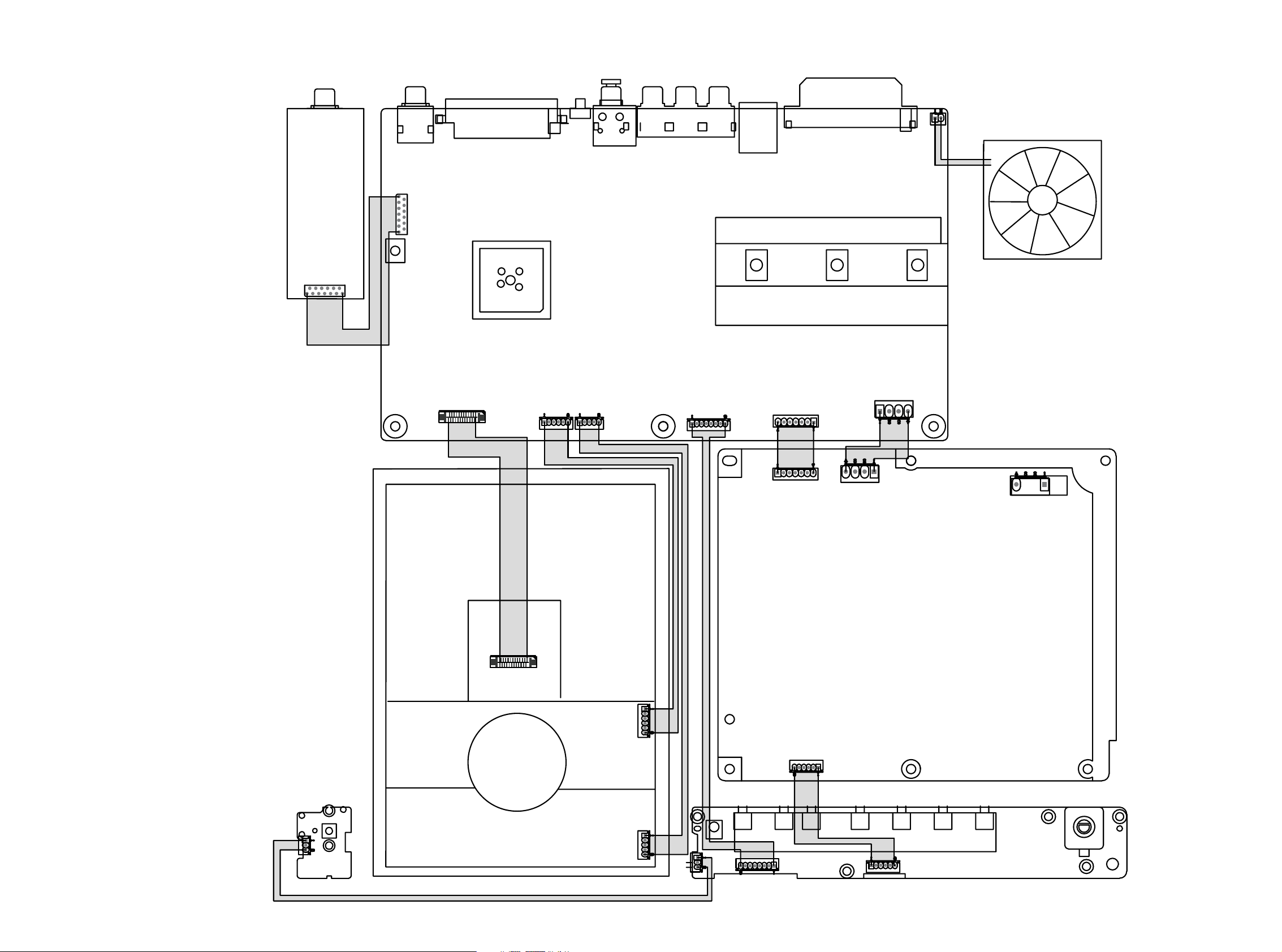
WIRING DIAGRAM - SCHEMA D'INTERCONNEXIONS - VERDRAHTUNGSPLAN - DIAGRAMMA DELLE INTERCONNESSIONI - ESQUEMA DE INTERCONEXIONES
DPL907VD - DPL907U - DPL2907 - DPL913VD - DPL2913 - DPL930VD - DPL2930
CN501
CN306
TUNER BOARD
CON01
CN101
MAIN BOARD
CN102
CN103
DVD
BOARD
CN305
CN302
CN2
FAN
CN304
CN1
AC IN
STANDBY
BOARD
RB704
L_CN1
L_CN2
L_CN3
RB703
RB701
SMPS BOARD
CN3
RB702
CONTROL BOARD
Page 3
5
ASMP1020 / ASMP1020D / ASMP1030
6 First issue 01 / 05
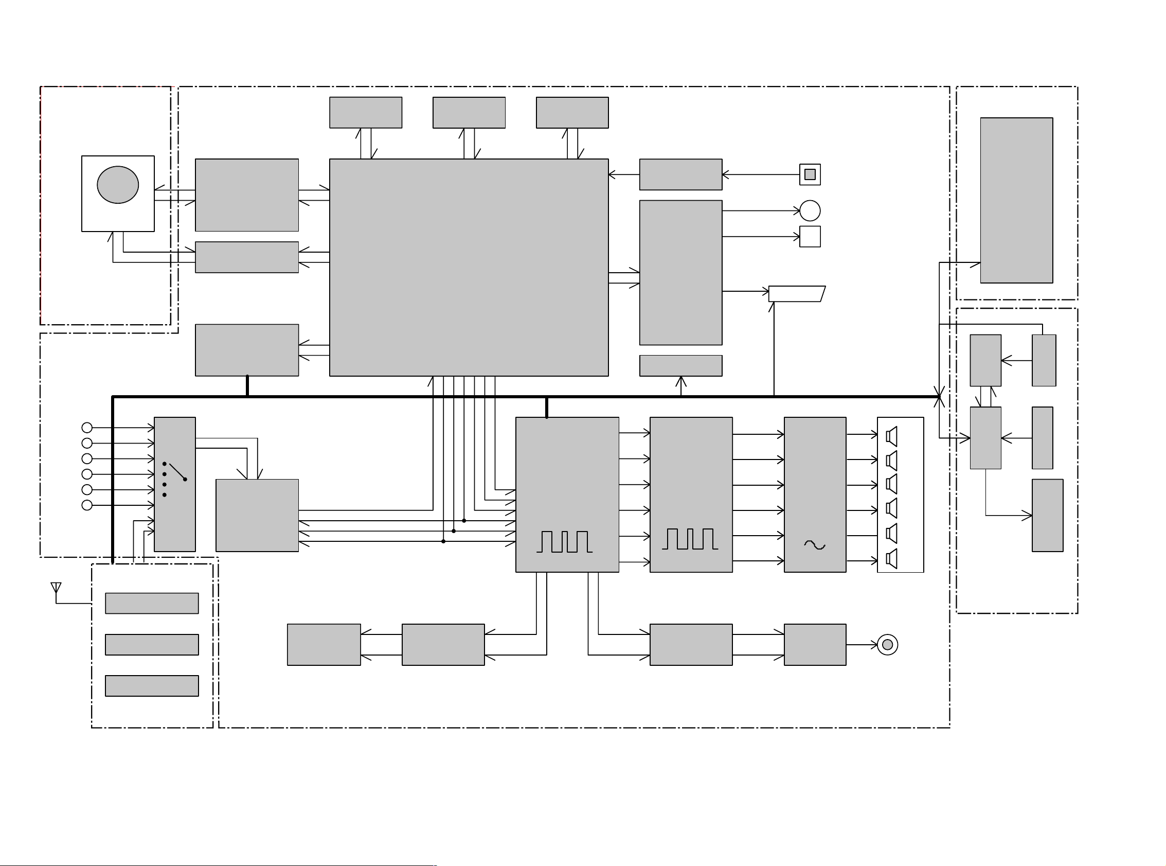
BLOCK DIAGRAM - SCHEMA SYNOPTIQUE - BLOCKSCHALTBILD - SCHEMA A BLOCCHI - ESQUEMA DE BLOQUES
LOADER
HR-M04P
MAIN BOARD
DVD Servo RF IC
ES6603
DVD MOTOR Drive IC
AT5868
EXPAND
I/O PORT
74F374*2
FLASH
SST39VF080 8M
SDRAM
4*16M
ESS6629✤ or ESS6698
MPEG II DECODER
DTS Decoder
DOLBY DIGITAL Decoder
DOLBY PRO LOGIC Decoder
WMA Decoder
✤
or DIVX Decoder
MP3 Decoder
TV ENCODE
Progressive Scan
u-com
✦✧
✦✧
EEPROM
24C02
✧
74HC04
Digital Buffer
VIDEO FILTER
VIDEO SW
SPDIF IN
POWER BOARD
SWITCH
✧
OPTICAL
CVBS
S-VIDEO
SCART
✧
POWER
POWER PCB
ASSY
230V 200W
STB CPU
CTM8B56EP
SENSOR
REMOTE
AUX1
AUX2
TV IN
FM
AUDIO
INPUT
SELECT
CD4052
TUNER
TUNER: KS 0302
PLL: LC72131M
RDS: LC 72723
TUNER BOARD
CS5333 or
CS5342
2CH AUDIO A/D
✧
✧
RJ45
Wireless output
✤
DPL907VD, DPL907U and DPL2907 only
✦
DPL913VD and DPL2913 only
✧
DPL930VD and DPL2930 only
RC4558
Lowpass filter
✧
Digital Audio Processor
Bass and Trebble Control
6 CH Volume Control
Bass management
DX-8001
STA308A
POWER
AMPLIFIER
DDX-2100✤✦ x 2
✤✦
STA505
STA505
x 2
✧
x 3
RC4558
Lowpass filter
✧
FL
FR
C
SL
SR
SUB
✤✦
✤✦
FILTER
APA3541
Phone AMP
FL
FR
C
✤✦
SL
✤✦
SR
SUB
✧
PHONE OUTPUT
FR
FL
C
✤✦
SL
SR
SUB
SPEAKER
OUTPUT
✤✦
PT6311
VFD DRIVE
KEY ARRAY
VFD
HNA-11SM51T
FRONT PANEL
BOARD
✧
Page 4
ASMP1020 / ASMP1020D / ASMP1030
First issue 01 / 05 7
8
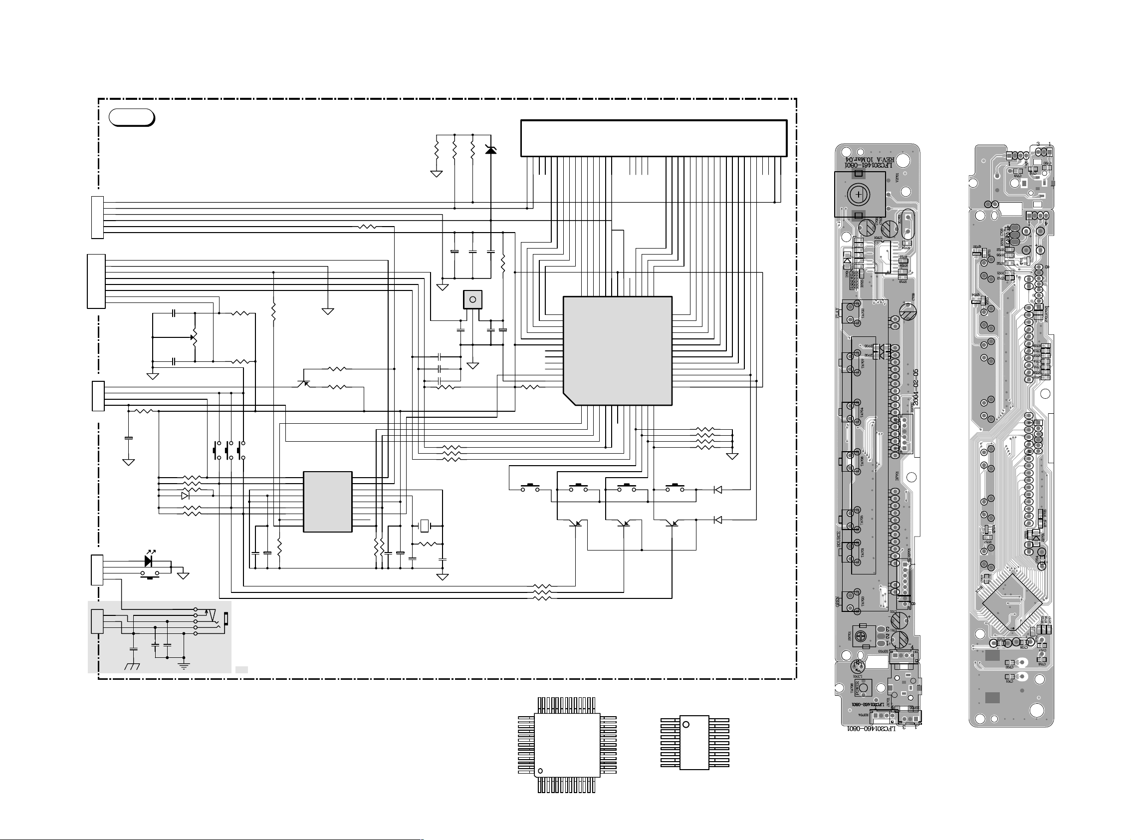
CONTROL / DISPLAY SCHEMATIC DIAGRAM - SCHEMA COMMANDES / AFFICHEUR - SCHALTBILD BEDIENTEIL / ANZEIGE SCHEMA COMANDI / INDICATORE - ESQUEMA MANDOS / INDICADOR
Controls / display P.C.B.
Platine commandes / afficheurs
Ltpl. Bedienteil / Anzeige
Piastra comandi / indicatore
Platina de mandos / indicadores
Component side
Côté composants
Bestückungsseite
Lato componenti
Lado componentes
Solder side
Côté cuivre
Lötseite
Lato saldature
Lado del cobre
KDB
DPL907VD - DPL907U - DPL2907 - DPL913VD - DPL2913 - DPL930VD - DPL2930
PT6311
MCU2116
DP701
ZD701
5.6V
R730
100
11SM51T
123456789
100K
R731
TA704
KEYC
R711 10K
R712 10K
R713 10K
1011121314151617181920212223242526272829303132333435363738
30
39
40
GR5
41
GR4
42
GR3
43
GR2
44
GR1
45
VDD
46
LED5
47
LED4
48
LED3
49
LED2
50
LED1
51
GND
52
OSC
TA705
Q702
A733
34
33
36
GR837GR738GR6
SW11SW22SW33SW44DOUT5DIN6NC7CLK8STB9K110K211K312K4
KEYC
35
VEE
SG20/GR9
SG19/GR10
IC702
PT6311
Q703
A733
32
VDD
SG18/GR11
TA706
31
SG11/KS11
SG17/GR12
SG10/KS10
KEYC
SG9/KS9
SG8/KS8
SG7/KS7
SG6/KS6
SG5/KS5
SG4/KS4
SG3/KS3
SG2/KS2
SG1/KS1
13
SG1327SG1428SG1529SG16
SG12
VDD
TA707
Q704
A733
26
25
24
23
22
21
20
19
18
17
16
15
14
R714 10K
R715 10K
R716 10K
R717 10K
KEYC
D702
1N4148
D703
1N4148
RB702
6
5
4
3
2
1
CON6
RB701
8
7
6
5
4
3
2
1
CON8_2.0
RB703
1
2
3
4
CON4_2.0
RB704
1
2
3
4
RB705
1
2
3
AC2
AC1
GND
-24V
PSW
B5V
ST_MUTE
GND
IR
VFD-DA
VFDCLK
VFDCE
ENCODE2
ENCODE1
C718
102
C721 10UF
R732
4.7K
LD701
TA708
KEYB
C719
102
C701
100P
VR3D
3
VR701
C702
100P
R703 10K
R704 10K
R705 10K
D701 1N4148
R706 10K
R707 10K
C720
102
2
1
JK701
CKX3.5-07
TA701KEYC
10K
R701
10K
R702
TA702KEYC
TA703KEYC
C703 104
C708 10UF
R721
560
R723 10K
Q701
A733
1
2
3
4
5
6
7
8
9
R708 10K
R722 560
IC701
MCU2116
POWER
SOURCE
GND
RESET
GND
PLAY
OPEN
F1
LOADER
IR
R718 1K
MUTE
PCON
XOUT
XIN
VDD
F3
OFF
F2
R719
1K
C709
100UF
R720
C704
104
1K
C707
104
R725
22K
SN701
REM
123
100UF
221
C712
C713
15P
C714
15P
C715
15P
R727 100
R728 100
R729 100
18
17
16
15
14
13
12
11
10
R710 10K
R709 10K
C706 104
C710 100UF
XL701
4M
R724
100K
C716
22PF
C717
22PF
104
C711
C705
R7264.7K
39
DPL930VD and DPL2930 only
2739
40
52
26
14
113
118
910
Page 5
9
ASMP1020 / ASMP1020D / ASMP1030
10 First issue 01 / 05
F1
4A/ 250V
ZNR1
275V
CX1
0.47 UF
/275V
+
C102
390UF /200V
LF 1
R102
390K
R105
100K/2W
C104
472/1KV
D103
BYV26E
C112
472/1KV
R116
100K/2W
U2A
PC817C
R119
6R8
T1
ER35
R206
1K
R208
2K4/ 1%
U5
TL431
C208
224
R205
47 K
+
C207
2.2UF/
50V
R207
30K/1%
AC 1
AC 2
CX2
0.47 UF
/275V
LF 2
1
234
5
6
7
8
U1
UC3845
R113
1K5
R108
10K
R106
10K
R107
15K 1%
R114
10K
C101
104
C107
47 2
C106
102
U2B
PC817C
D104
1N4148
D105
1N4148
C105
104
+
C110
6.8UF/ 50V
C108
101
C109
102
R109
300R
R122
5K1
R121
1K
D101
1N4148
Q102
6N90
R112
0.33 R/2W
T2
EE22
D106
BYV26E
D107
BYV26E
+
C114
470U F/
35V
ZD101
22V /1W
R120
100R
U3B
PC817A
+
C113
47 UF/16V
CL201
T106 52
R201
10K
C202
102
+
C206
1500UF/
50V
R204
10K
L202
R209
10K
D204
BYV26E
+
C211
47 UF/5 0V
+
C214
100UF/16V
R211
1K
R212
1K
D205
SB56 0
+
C212
470UF /16V
R213
1K
R224
1K
D209
BYV26E
+
C219
220UF /16V
R221
1K
R223
1K
ZD201
5V1
+33V
PSon
S+5V
-12V
VFD+
VFD-
+32V
RTN
S+5V
GND
+5V
GND
+12V
-12V
GND
PSon
-31V
GND
VFD+
VFD-
5Vsb
Vr ef
VDD
VDD
1
23
4
BR1
GBJ4 08
114T
25T3 T
13T
7T
7T
22T
66T
HV
HV
3
2
5
1
14,15,16
12,13
5,6,7
1,2,3
6
8
4
3
3
2
1
R202
2K
C201
102
R210
56 R
C209
102
ZD202
3.3V
RT1
2R5
+
C103
390UF /200V
R103
330 K
R104
330 K
S1
1
2
3
D201
ST PR1620CT
L201
1
2
3
D202
ST PR1620CT
R203
2K
C203
102
+
C205
1500UF/
50V
RT N
R218
10R
C210
102
+
C220
2200UF /10V
R222
150R
+5V
GND
6T
+
C221
470UF /10V
L203
+
C213
220UF /16V
D203
BYV26E
Q201
C1815
Q202
C1815
5Vsb
+12V
D207
SB160
R219
10R
D208
BYV26E
+
C218
220UF/ 35V
R220
5K6
-31V
20T
11
8
GND
D212
1N4148
U3A
PC817C
R215
150R
R217
3K24 /1%
U6
TL4 31
C217
224
R214
10K
+
C216
100UF
/16V
R216
3K24 /1%
3
2
1
GND
1
2
3
4
5
6
CN3
1
2
3
4
5
6
7
CN2
1
2
3
4
CN1
1
2
3
4
CN4
C
1
M
3
S
4F5
D
7
U4
TO P233Y
R118
1K
R117
43 R/1W
C215
104
C222
104
CY3
47 1
CY4
47 1
CY5
332
HV
D108
BYV26E
12
3
Q502
C1815
Q501
C1015
R503
1K
R502
10K
R501
2K
ZD50 1
12V
C501
104
C224
104
R225
1K
+
C225
22UF /16V
L204
R226
1K
60T
11
9
7
10
C226
104
C229
104
C228
104
C230
104
C231
104
Q301
2N7000
ZD30 1
15V
R302
200K
C302
101
R303 B
1M
Q302
2N7000
ZD30 2
15V
R304
200K
C30 3
101
R301A
1M
AC
D301
1N4007
AC HV
C30 1
472/1KV
1
2
3
1
3
2
R301B
1M
R303 A
1M
D210
1N4007
+33V
R101
1N4007
!
!
!
!
!
!
!
!
!
!
!
!
!
!
!
!
!
!
!
!
!
POWE
CONTROL
21.7
20.8
0.7
1.1
4.9
21.6
0.4
0
305
21.6
19
4.9
0.7
11.5
4.9
-32.4
-11.8
-26.3
-26
4.9
-26
33
305
T=7µs
5.5Vpp
2Vpp
1V
0
600Vpp
0
0
T=7µs
440Vpp
T=7µs
Indicates critical safety components, and
identical components should be used for
replacement.
Only then can the operational safety be garanteed.
Le remplacement des éléments de sécurité
(repérés avec le symbole ) par des composants
non homologués selon la Norme CEI 65 entraine la
non-conformité
de l'appareil. Dans ce cas, la responsabilité du
fabricant n'est plus engagée.
!
!
!
!
Wenn Sicherheitsteile (mit dem Symbol
gekennzeichnet) durch nicht
normgerechte Teile ersetzt werden, erlischt die
Haftung des Herstellers.
La sostituzione degli elementi di sicurezza
(marcati con il segno )
con componenenti non omologati secondo la norma
CEI 65 comporta la non conformitá dell'apparecchio.
In tal caso é “esclusa la responsabilità” del costruttore.
La subtitución de elementos de seguridad
(marcados con el simbolo ) por componentes no
homologados segun la norma CEI 65, provoca la no
conformidad del aparato.
En ese caso, el fabricante cesa de ser responsable.
!
Part of board connected to mains supply.
Partie du châssis reliée au secteur.
Primärseite des Netzteils.
Parte dello telaio collegata alla rete.
Parte del chasis conectada a la red.
Use isolating mains transformer
Utiliser un transformateur isolateur du secteur
Einen Trenntrafo verwenden
Utilizzare un transformatore per isolarvi dalla rete
Utilizar un transformador aislador de red
!
Note :
Power Supply primary circuit measurements.
- Use only ( ) connection point.
Attention :
Mesure dans la partie primaire de l'alimentation
- Utiliser la masse du bloc alimentation ( ).
Achtung :
Bei Messungen im Primärnetzteil
- Primärnetzteilmasse verwenden ( ).
Attenzione :
misure nell'alimentatore primario
- usare massa alimentazione primario ( ).
Cuidado :
Medida en el bloque de alimentacion
- Utilizar la masa del bloque de alimentacion ( ).
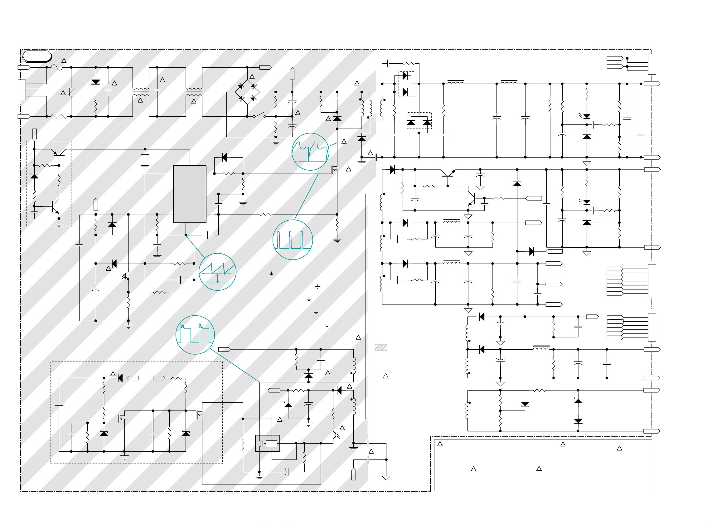
POWER SUPPLY SCHEMATIC DIAGRAM - SCHEMA DE L'ALIMENTATION - SCHALTBILD NETZTEIL - SCHEMA DELL' ALIMENTAZIONE - ESQUEMA DE LA ALIMENTACIÓN
DPL907VD - DPL907U - DPL2907 - DPL913VD - DPL2913
POWE
Page 6
ASMP1020 / ASMP1020D / ASMP1030
First issue 01 / 05 11
Power supply P.C.B.
Platine alimentation
Ltpl. Netzteil
Piastra alimentazione
Platina alimentación
U1 UC3845
Component side
Côté composants
Bestückungsseite
Lato componenti
Lado componentes
DPL907VD - DPL907U - DPL2907 - DPL913VD - DPL2913
UC3845
PC817A
TOP233Y
Vref
8
INTERNAL
BIAS
Vfb
2
Comp
1
Current Sense
3
Rt/Ct
4
1/2 Vref
Err
Amp
5V Vref
Set/Reset
Oscillator
18
45
Vcc
1
7
U.V.L.O
LOGIC
LOGLC
1/3
1V
C.S.
Comp
PMW Latch
RS
T
36V
Pwr Vc
Pwr Gnd
Gnd
Output
5
7
6
5
2
1 C3 M5 F4 S7
D
4
3
Page 7

ASMP1020 / ASMP1020D / ASMP1030
12 First issue 01 / 05
DPL907VD - DPL907U - DPL2907 - DPL913VD - DPL2913
U4 TOP233Y
Power supply P.C.B.
Platine alimentation
Ltpl. Netzteil
Piastra alimentazione
Platina alimentación
Solder side
Côté cuivre
Lötseite
Lato saldature
Lado del cobre
2SK2749
G
D
S
2N7000
S
G
D
2SC1815
E
C
B
CONTROL
C
M
F
MULTIFUNCTION
FREQUENCY
(Y Package
Only)
V
C
Z
C
SHUNT REGULATOR/
ERROR AMPLIFIER
-
+
I
FB
CURRENT
LIMIT
ADJUST
V
+ V
BG
V
BG
LINE
SENSE
R
E
5.8 V
4.8 V
5.8 V
V
I (LIMIT)
ON/OFF
T
OV/UV
DC
MAX
OSCILLATOR WITH JITTER
+
-
INTERNAL UV
COMPARATOR
STOP
DC
MAX
HALF
FREQUENCY
SOFT-
START
D
CLOCK
0
INTERNAL
SUPPLY
1
SOFT
START
8
SHUTDOWN/
AUTO-RESTART
HYSTERETIC
THERMAL
SHUTDOWN
MAX
SAW
-
+
PWM
COMPARATOR
SRQ
Q
-
+
CURRENT LIMIT
COMPARATOR
CONTROLLED
TURN-ON
GATE DRIVER
LEADING
EDGE
BLANKING
DRAIN
SOURCE
D
S
Page 8

ASMP1020 / ASMP1020D / ASMP1030
First issue 01 / 05 13
Power supply P.C.B.
Platine alimentation
Ltpl. Netzteil
Piastra alimentazione
Platina alimentación
U4 KA5L038R
DPL930VD - DPL2930
Component side
Côté composants
Bestückungsseite
Lato componenti
Lado componentes
LTV817
KA5L038R
KA7500C
E13009
B
C
E
KTA1023
E
C
B
1
2
4
3
4
1
116
89
Vcc
3
FB
4
5uA
7.5V
27V
UVLO
1 mA
+
_
+
_
2.5R
9V
1R
THERMAL S/D
S
Q
R
INTERNAL
BIAS
POWER ON RESET
Vref
OSC
_
+
5V
GOOD
LOGIC
L.E.B
DRAIN
2
SFET
S
Q
R
Rsens
GND
1
Page 9

ASMP1020 / ASMP1020D / ASMP1030
14 First issue 01 / 05
Power supply P.C.B.
Platine alimentation
Ltpl. Netzteil
Piastra alimentazione
Platina alimentación
U1 KA7500C
Solder side
Côté cuivre
Lötseite
Lato saldature
Lado del cobre
DPL930VD - DPL2930
BCE
FDN360P
ECB
BT3906
R
6
T
5
C
T
DEAD
4
TIME
CONTROL
EA (+)
1
+
1
EA (-)
EA (+)
EA (-)
_
2
16
+
2
_
15
OSCILLATOR
1.2V
PWM
COMP
0.7MA
OUTPUT CONTROL
Q
D
CK
Q
13
5V
BAND GAP
REFERENCE
8
9
11
10
12
14
7
C1
E1
C2
E2
V
CC
V
REF
GND
3
COMP INPUT
Page 10

ASMP1020 / ASMP1020D / ASMP1030
First issue 01 / 05 15
16
POWER SUPPLY SCHEMATIC DIAGRAM - SCHEMA DE L'ALIMENTATION - SCHALTBILD NETZTEIL - SCHEMA DELL' ALIMENTAZIONE - ESQUEMA DE LA ALIMENTACIÓN
DPL930VD - DPL2930
POWE
1.0 / (1.1)*
1.0 / (1.1)*
1.4 / (0.4)*
163.0
(5.0)*
46.0*
46.5
(4.6)*
Part of board connected to mains supply.
Partie du châssis reliée au secteur.
Primärseite des Netzteils.
Parte dello telaio collegata alla rete.
Parte del chasis conectada a la red.
4.8
(4,8)*
0.0
(2.4)*
1.7
(0.0)*
12.0 / (1.6)*
5.0 / (0.8)*
Use isolating mains transformer
!
Utiliser un transformateur isolateur du secteur
Einen Trenntrafo verwenden
Utilizzare un transformatore per isolarvi dalla rete
Utilizar un transformador aislador de red
32.2
18.0
T=20µs
0
500Vpp
357.0
163.0
1.4 / (0.3)*
12 / (1.5)*
5.0
(0.8)*
0.0 / (0.0)*
Note :
Power Supply primary circuit measurements.
- Use only ( ) connection point.
Attention :
Mesure dans la partie primaire de l'alimentation
- Utiliser la masse du bloc alimentation ( ).
Achtung :
Bei Messungen im Primärnetzteil
- Primärnetzteilmasse verwenden ( ).
2.5
0.0 / (0.0)*
3.6 / (0.0)*
1.5 / (0.0)*
0.0 / (0.0)*
3.6 / (0.2)*
2.52.5 / (0.4)*
(0.4)*
18.0
32. 2
Attenzione :
Misure nell'alimentatore primario
- usare massa alimentazione primario ( ).
Cuidado :
Medida en el bloque de alimentacion
- Utilizar la masa del bloque de alimentacion ( ).
Indicates critical safety components, and
!
identical components should be used for
replacement.
Only then can the operational safety be garanteed.
Le remplacement des éléments de sécurité
(repérés avec le symbole ) par des composants
non homologués selon la Norme CEI 65 entraine la
non-conformité
de l'appareil. Dans ce cas, la responsabilité du
fabricant n'est plus engagée.
!
*: ON / (Standby)
-26.9 / (-4.0)*
-12.9 / (-1.5)*
-22.0 / (-1.0)*
-22.0 / (-1.0)*
Wenn Sicherheitsteile (mit dem Symbol
gekennzeichnet) durch nicht
normgerechte Teile ersetzt werden, erlischt die
Haftung des Herstellers.
La sostituzione degli elementi di sicurezza
(marcati con il segno )
con componenenti non omologati secondo la norma
CEI 65 comporta la non conformitá dell'apparecchio.
In tal caso é “esclusa la responsabilità” del costruttore.
GND
!
-12.9 / (-1.5)*
12.0 / (1.5)*
5.0 / (0.8)*
!
La subtitución de elementos de seguridad
(marcados con el simbolo ) por componentes no
homologados segun la norma CEI 65, provoca la no
conformidad del aparato.
En ese caso, el fabricante cesa de ser responsable.
!
4.8 / (4.8)*
1.7 / (0.0)*
-26.9 / (-4.0)*
-22.0 / (-1.0)*
-22.0 / (-1.0)*
Page 11

17
ASMP1020 / ASMP1020D / ASMP1030
18 First issue 01 / 05
MAIN SCHEMATIC DIAGRAM - SCHEMA DE LA PLATINE PRINCIPALE - GRUNDPLATTE SCHALTBILD - SCHEMA DELLA PIASTRA PRINCIPALE- ESQUEMA DE LA PLATINA PRINCIPAL
(1/3)
DPL907VD - DPL907U - DPL2907 - DPL913VD - DPL2913 - DPL930VD - DPL2930
MAIN
C111
CN101
RFGND
24
LD-GND
23
DVDLDO
DVD-LD
22
NC
21
RF50V
HFM-VCC
20
PD
MPD
19
CDLDO
CD-LD
18
VR-DVD
DVD-VR
17
VR-CD
CD-VR
16
NC
15
PUH-E
E
RF50V
14
VCC
13
PVC
VC(Vref)
RFGND
12
GND
PUH-F
11
F
10
PUH-A
B
9
PUH-B
A
8
DVDRF
RF
7
CD-DVD
CD/DVD SW
6
PUH-C
D
5
PUH-D
C
4
TRACK-
T-
3
TRACK+
T+
2
FOCUS-
F+
1
FOCUS+
F-
RF50V RF50V
R101
104
18K
C106
Q102
104
2SK3018
C105
Q103
2N3904
C101 100uF
RFGND
SLEGN
OPEN
15K
R105
R110
1M
R111
MVCC
C123
104
CN102
LOAD-/DCMO-
6
LOAD+/DCMO+
5
4
HOMESW
3
SLED+
2
SLED-
1
CN103
DCLOAD-
5
DCLOAD+
4
OUTSW
3
2
INSW
1
✤
DPL907VD, DPL907U and DPL2907 only
✦
DPL913VD and DPL2913 only
✧
DPL930VD and DPL2930 only
C102
100uF
R114
4.7K
FOCUS
G
R112
56K
OPEN
CLOSE
DCLOAD-
DCLOAD+
SLED-
SLED+
FOCUS-
FOCUS+
D
S
RFGND
R102
100K
D
S
1
2
3
4
5
6
7
8
9
10
11
12
13
14
Q101
2SK3018
R126
G
VINFC
OP2IN-
OP2IN+
VINSL+
OP2OUT
FWD
REV
VCC1
VOTR-
VOTR+
VOSL+
VOSL-
VOFC-
VOFC+
10K
Q104
2N3904
IC101
AM5868
GND29GND
30
CDLDO
DVDLDO
VINTK
OP1IN+
OP1IN-
VINLD
OP1OUT
VOLD-
VOLD+
VOTK-
VOTK+
MUTE
BIAS
GND
VCTL
VCC2
RFGND
RF50V
FB116
601
2SB1132
2SB1132
FB117
601
MVCC
C107
104
Q105
Q106
RFGND
28
27
26
25
24
23
22
21
20
19
18
17
16
15
C128
104
C141
680PF
PUH-B
PUH-A
PUH-D
PUH-C
D101 1N4148
R135
OPEN
R127
10K
100uF
C151
LOAD-/DCMO-
LOAD+/DCMO+
TRACK-
TRACK+
C108
104
C145
102
R133
10
R134
10
D102
1N4148
R113
56K
R115
OPEN
C127
472
C140
680PF
C142
680PF
C144
100PF
C146
102
RF50V
104
104
C112
C113
820PF
59
58
63
62
60
57
64
61
AIP
AIN
VPA
ATOP
RFAC
RFDC
ATON
RFSIN
1
DVDFRP
2
DVDRFN
3
A2
4
B2
5
C2
6
C143
D2
680PF
7
CP
8
CN
9
D
10
C
11
B
12
A
13
CD_D
14
CD_C
15
CD_B
16
CD_A
PUH-F
PUH-E
RFGND
PVC
DVDLD
C103
100uF
RF50V
C104
100uF
CDLD
RFGND
D103
RESET#
1N4148
R106
1K
MVCC
C110
104
R128
10K
R129
10K
C109
104
IC102
ES6603
CD_F17CD_E18VPB19VC20DVDLD21CDLD22DVDPD23CDPD24VNB25LDON26MIRR27MP28MB29MLPF30MIN31MEVO
RFGND
RESET#
SPDON
SVREF15-
TRACK
SPINDLE
R142
1.5K
R143
1.5K
VCC
IC103
AT24C02N
1
S0
VCC
2
S1
WC
3
S2
SCL
GND4SDA
SERIAL EEPROM
C152
C153
470PF
470PF
C124
104
R141
50
56
55
54
53
52
51
49
12K
RX
DIP
DIN
FNP
BYP
FNN
VNA
MEV
SDEN
SDATA
SCLK
V33
LCP
LCN
MNTR
CE
FE
TE
PI
V25
V125
TPH
DFT
LINK
32
MEVO
224
C154
C155
160PF
C125
104
R144
22K
R145
22K
C164
C157
10uF
8
7
6
5
104
RF33V
RF50V
C165
103
RFGND
RFGND
RF33V
48
47
46
45
C170
44
473
43
42
41
40
39
38
37
36
35
C116
34
104
33
C156
103
MIRRA
SLDC
R160
OPEN
R117
R116
4.7K
4.7K
C167
33PF
SCSJ
SDATA
SCLK
CEI
FEI
TEI
SBAD
SVREF15
DEFCT
C115
C114
104
104
R178
C168
33PF
C169
33PF
DIN
C184
472
PLLGND
C178
47PF
R170
R
R171
1.2K
104
INSW
HOMESW
CLOSE
OUTSW
OPEN
MOCTL
AUX4
AUX5
AUX6
AUX7
IC105
LM809
VCC3RST
C130
104
C118
R131
G
1
C173
R130 10K
DIP
C185
C131
104
C172
C
C
C174
473
C175
560PF
R172
5.1K
10K
CD_DVD_CT
R174 6.8K
R175 6.8K
R177 0
R176 6.8K
R136
0
R161 33
R162 33
R163 33
R107 1K
R108
2
R103
100K
472
C132
104
RF33V
C133
104
TR1
TR2
C119
104
XSCSJ
XSDATA
XSCLK
DEFCT
SLDC
SPDON
1K
RESET#
L101
3.3uH
C190
102
R146
0 OHM
RESET#
C183
103
RFGND
R104
100K
XL101
27M
R148
0 OHM
R173
33K
C176
470PF
R169
150
Q107
A733
IR
VFD-DA
SCAR_SW
RDS_SCL
C189
27PF
C179
EAUX3
EAUX2
EAUX1
EAUX0
AUX0
AUX1
AUX2
AUX3
1uF
C166
682
MVCC
RF33V
C129
104
RFGND
TR1
TR2
C117
104
C177
470PF
RA103 33*4
1 8
2 7
3 6
4 5
VCC33
C126
104
RF50V
RF50V
C171
333
TESTAD
MIRRA
SVREF15
C182
153
SPINDLE
FOCUS
SLEGN
TRACK
SCSJ
SDATA
SCLK
C188
27PF
RA10133*4
1 8
TU_LED
2 7
ST_LED
3 6
TU_DOUT
4 5
RDS_SDA
RA10233*4
I2C_DATA
1 8
I2C_CLK
2 7
3 6
ENCODE1
ENCODE2
4 5
VCC
R137
4.7K
R138
4.7K
CEI
3.3K
R180
3.3K
R132
10K
C186
4.7uF
C180
1uF
C181
1uF
MIRRA
SVREF15
SVREF09
SVREF21
146
147
148
149
150
XSRFRP
AVDD3_AD
XSVREF[21]
XSVREF[09]
XSVREF[15]
DMA3
DMA2
DMA4
3 6
4 5
MA2
MA3
RA10610x4
182 7
MA4
32/64MBIT SDRAM
23
A0
24
A1
25
A2
26
A3
29
A4
30
A5
31
A6
32
A7
33
A8
34
A9
22
A10
35
A11
38
CLK
37
CKE
19
CS
18
RAS
17
CAS
16
WE
15
DQML
39
DQMH
20
BA0
21
BA1
36
NC
40
NC
145
DMA5
MA5
R181
3.3K
144
XSTEI
DMA6
3 6
MA6
IC104
R179
XSCEI
FEI
TEI
SBAD
C120
104
68K
20K
R149
0 OHM
C252
5PF
C187
682
RFGND
157
158
159
160
161
162
163
164
165
166
167
168
169
170
171
172
173
174
175
176
177
178
179
180
181
182
183
184
185
186
187
188
189
190
191
192
193
194
195
196
197
198
199
200
201
202
203
204
205
206
207
208
R182
R183
154
151
152
153
155
156
XSIPIN
XSIREF
XSRFIP
XSRFIN
XSDSSLV
AVDD3_DS
AVSS_DS
AVSS_PL
XSPDOFTR1
XSFDO
XSFTROPI
AVDD3_PL
XSPLLFTR1
XSPLLFTR2
XSVREF0
XSAWRC
AVSS_DA
XSRFRPCTR
XSTRAY
AVDD3_DA
XSSPINDLE
XSFOCUS
XSSLEGP
XSSLEGN
XSTRACK
XSTESTDA
XSFGIN
XSPHOI
SXCSJ
XSDATA
XSCLK
XSDFCT
XSLDC
XSSPDON
VD33
VS33
XGPIO[9]
XGPIO[8]
XGPIO[7]
XGPIO[6]
XGPIO[5]
XGPIO[4]
EAUX03
EAUX02
EAUX01
EAUX00
VSS
VDD
AUX0
AUX1
AUX2/ HSYNC
AUX3/ VSYNC
AUX4
AUX5
AUX6
AUX7
RESET
VS33
VD331XIN2XOUT3DCLK4DMA05DMA16DMA27DMA38VS339VD3310DMA411DMA512DMA613DMA714DMA815DMA916DMA1017VS3318VD3319DMA1120DCAS21DCS022DCS123DRAS024DBANK0/ DRAS125VSS26VDD27DBANK1/ DRAS228DCKE/DOE/TDMTSC
XIN
DCLK
XOUT
DMA1
DMA0
RA10510x4
1 8
2 7
MA1
MA0
MA0
MA1
MA2
MA3
MA4
MA5
MA6
MA7
MA8
MA9
MA10
MA11
R151
33
DSCK
R152
DOE#
33
CS0#'
RAS0#'
CAS#'
DWE#
R156 33
DQM
R157
33
RAS1#'
RAS2#
R159
33
4Mx16 SDRAM (9ns)
3.3K
143
DMA7
4 5
MA7
142
XSFEI
AVSS_AD
DMA8
DQ0
DQ1
DQ2
DQ3
DQ4
DQ5
DQ6
DQ7
DQ8
DQ9
DQ10
DQ11
DQ12
DQ13
DQ14
DQ15
VCC
VCC
VCC
VCCQ
VCCQ
VCCQ
VCCQ
VSSQ
VSSQ
VSSQ
VSSQ
VSS
VSS
VSS
141
DMA9
RA10710x4
TESTAD
140
XSSBAD
XSTESTAD
DMA10
1 8
MA8
139
XSTEXI
2 7
MA9
C147
102
C149
102
VCC20
XFLAG2
XFLAG1
XFLAG3
137
138
134
135
136
VSS
VDD
XSFLAG[1]
XSFLAG[2]
XSFLAG[3]
ESS6629✤ or ESS6698
CS0#
CAS#
DMA11
3 6
4 5
MA10
MA11
1 8
2 7
CAS#'
CS0#'
2
DB0
4
DB1
5
DB2
7
DB3
8
DB4
10
DB5
11
DB6
13
DB7
42
DB8
44
DB9
45
DB10
47
DB11
48
DB12
50
DB13
51
DB14
53
DB15
1
14
27
3
9
43
49
6
12
46
52
28
41
54
C148
102
C150
102
RFGND
RXD
XFLAG0
132
133
XSFLAG[0]
RAS0#
RAS1#
5
3 6
4
RAS0#'
RAS1#'
TXD
131
130
XSIP2
XSIP1
IC106
Vibratto-II
RA108 33x4
SVCC33
TBCK
SPDIF
TSD3
SPDIF-IN
119
122
123
125
127
126
128
129
VS33
VD33
XSLG
XSWBL
XSWBLCLK
DWE30DB031DB132DB233VS3334VD3335DB336DB437DB538DB639DB740DB1541DB1442VS3343VD3344DB1345DB1246DB1147DB1048DB949DB850DSCK51VS33
29
DB1
DB0
DOE#
DWE#
RAS2#
VCC33
FB118
601
120
121
124
TSD2
TSD3
TBCK
MCLK
SPDIFIN
SPDIF/SEL_PLL3
✦✧
DB3
DB5
DB4
DB2
PLL2
0
01
0
0
1
1
VIDEO OUTPUT TABLE
VDAC
YDAC
CDAC
UDAC
FDAC
PLL30CLK SOURCE
1
118
VS33
DB6
PLL1
CVBS + S-VIDEO + UV
R121
4.7K
4.7K
R119
4.7K
4.7K
R122
R120
R118
YDAC1
UDAC1
CDAC1
113
114
115
YUV5/YDAC
YUV2/CDAC
YUV0/UDAC
TWS/SEL_PLL2
DB14
PLL0
0
0
1
01
1
0
1
CVBS
Y
V
U
C
FDAC1
GNDV
VDAC1
VCC33V
109
110
111
112
VS33_DA
VD33_DA
YUV7/FDAC
YUV6/VDAC
DB10
DB12
DB11
DB13
MULTI
DEFAULT
4.25
reserved 5
bypass
3.75
4.5
reserved
3.5
4
CVBS + YUV
CVBS
YG
V
U
CVBS
TWS
116
117
TSD0/SEL_PLL0
TSD1/SEL_PLL1
DB7
DB15
0
0
127bypass
1
0
0
11
1
DCLK INPUT
CRSTAL OSC
4.7K
RSET
108
YUV4/RSET
RBCK/TDMCLK
DB9
S-CHIP
4.5
4.25
4.75
5.5
C135 OPEN
VCC33V
COMP
VS33_PL2
VREF
105
106
107
YUV1/VREF
YUV3/COMP
VD33_PLL
RWS/TDMFS
RSD/TDMDR
LWRLL
DB8
DSCK
4
6
S-VIDEO + RGB
C249 OPEN
VS33_PL
LD7
LD6
LD5
LD4
VD33
VS33
LD3
LD2
LD1
LD0
LOE
LCS3
VDD
VSS
LCS2
LCS1
LCS0
LA0
LA1
LA2
VD33
VS33
LA3
LA4
LA5
LA6
LA7
LA8
VDD
VSS
LA9
LA10
LA11
LA12
LA13
LA14
LA15
VD33
VS33
LA16
LA17
LA18
LA19
LA20
LA21
DQM
VD33
52
DEFAULT
114.75
101.25
121.5
NA
NA
94.5
108
C250 OPEN
Y
R
B
C
R164
0 OHM
R155
0 OHM
0 OHM
104
103
102
101
100
99
98
97
96
95
94
93
92
91
90
89
88
87
86
85
84
83
82
81
80
79
78
77
76
75
74
73
72
71
70
69
68
67
66
65
64
63
62
61
60
59
58
57
56
55
54
53
Frequency
SPDIF-IN
SPDIF
AMCLK
SD2
SD1
SD0
LRCK
R184
390
C122
104
R185
S-CHIP
121.5
135
NA
108
114.75
128.25
148.5
162
CVBS + RGB
CVBS
G
R
B
CVBS
SPDIF
BICK
R165
0 OHM
SD2
SD0
C121
104
VD33_PL1
RWS
RBCK
RSD
LD7
LD6
LD5
LD4
LD3
LD2
LD1
LD0
LOE#
WRLL#
LCS3#
LCS2#
LCS1#
LA0
LA1
LA2
LA3
LA4
LA5
LA6
LA7
LA8
LA9
LA10
LA11
LA12
LA13
LA14
LA15
LA16
LA17
LA18
LA19
LA20
LA21
DQM
FB115
VCC20
601
SPDIF-IN
BICK
AMCLK
TSD3
SD1
LRCK
UDAC1
CDAC1
YDAC1
VDAC1
FDAC1
VCC33
VCC33V
LA20
VCC33
LCS2#
LD0
LD1
LD2
LD3
LD4
LD5
LD6
LD7
CN104
C191
22PF
R147 OPEN
R150
OPEN
R153
R154
OPEN
R123 4.7k
4
7
8
13
14
17
18
1
11
OPEN
IC109
74F374
D03Q0
D1
D2
D3
D4
D5
D6
D7
OE
CLK
1234
VCC33V
ZD106
7.5V
TVIN_L
TVIN_R
SCAR_R
SCAR_L
FB108
601
FB109
601
FB110
601
FB111
UDAC
CDAC
YDAC
VDAC
FDAC
ZD112
7.5V
ZD115
7.5V
601
ZD113
7.5V
ZD114
7.5V
VCC33V
ZD107
7.5V
ZD108
7.5V
ZD109
7.5V
VCC33V
ZD110
7.5V
ZD111
7.5V
JK101
SK-12D01-VG6
FB106
601
FB107
B
G
R
CVBS1
R186
75 OHM
R188
75 OHM
R190
75 OHM
R167
33
C192
22PF
4
1
2
3
5
C158
10uF
C159
10uF
C206
15PF
601
C208
15PF
C210
15PF
C211
15PF
C213
15PF
L104
C194
2.4uH
470PF
C198
470PF
L108
2.4uH
C202
470PF
R166
33
LRCK
BICK
DOUT
R168
33
C193
22PF
SCAR_SW
C251
10uF
FB104
601
FB105
601
C204
C205 15PF
C207
15PF
JK102
1
AOR
AIR
3
AOL
AGND
5
B GND
AIL
7
B
SWTCH
9
G GND
CLKOUT
11
G
DATA
13
R GND
DATAGND
15
R
BLNK
17
VGND
BLNKGND
19
VOUT
VIN
21
SHIELD
SCART_21PIN
1
LA16
A15
2
LA15
A14
3
LA14
A13
LA13
4
A12
LA12
5
A11
LA11
6
A10
LA10
7
A9
8
LA9
A8
9
NC
10
NC
11
WRLL#
WE#
12
RESET#
RESET#
13
NC
14
NC
15
RY/BY#
LA19
16
A18
17
LA18
A17
18
LA8
A7
LA7
19
A6
LA6
20
A5
LA5
21
A4
22
LA4
A3
23
LA3
A2
LA2
24
A1
MBM29LV800BA
TU_PO
2
TU_CE
5
Q1
TU_DIN
6
Q2
TU_CLK
9
Q3
S-SWTCH
12
Q4
S-BLNK
15
Q5
DVD
16
Q6
FAN
19
Q7
IC107'
BYTE#
DQ15/A-1
48
LA17
A16
47
46
GND
LA0
45
LD7
44
DQ7
43
DQ14
LD6
42
DQ6
41
DQ13
LD5
40
DQ5
39
DQ12
LD4
38
DQ4
37
VCC
36
DQ11
LD3
35
DQ3
34
DQ10
LD2
33
DQ2
32
DQ9
LD1
31
DQ1
30
DQ8
LD0
29
DQ0
LOE#
28
OE#
27
GND
26
LCS3#
CE#
LA1
25
A0
VCC33V
C195
470PF
L106
2.4uH
C199
470PF
C203
470PF
FB102
FB103
601
LRCK
BICK
DOUT
TP113
EGND
C218
104
15PF
R109
2
FB112
4
601
6
8
10
C209
15PF
12
14
C212
15PF
16
18
20
LA16 LA17
LA15
LA14
LA13
LA12
LA11
LA9
LA8
WRLL#
VCC33
LA18
C134
104
LA7
LA6
LA5
LA4
LA3
LA2
LD0
LD1
LD2
LD3
LD4
LD5
LD6
LD7
LCS1#
FB113
VCC33V
601
1K
601
ZD103
7.5V
+12V_1
10
11
12
13
14
15
16
17
18
19
20
1
2
3
4
5
6
7
8
9
13
14
17
18
11
ZD102
7.5V
4
7
8
1
ZD104
7.5V
ZD105
7.5V
C217
102
Q110
CM5783
R187
75 OHM
R189
75 OHM
FB101
601
C215
47PF
C214
47PF
TP114
SCART(CVBS+RGB) OUT
EGND
Q108
CM5783
ZD101
7.5V
R192
R193
10K
10K
VCC
R125
Q109
CM5783
4.7K
R191
75 OHM
A16
A17
A15
GND
A14
A13
A19
A12
A10
A11
DQ7
A9
DQ6
A8
DQ5
WE#
DQ4
NC
VCC
NC
VCC
NC
A18
DQ3
SST
A7
DQ2
A6
DQ1
A5
DQ0
A4
OE#
A3
GND
A2
CE#
A1
IC107
SST39LF080/016
IC108
74F374
2
D03Q0
5
Q1
D1
6
D2
Q2
9
Q3
D3
12
D4
Q4
15
Q5
D5
16
D6
Q6
19
D7
Q7
OE
CLK
R124
4.7K
CM5783
NC
NC
A0
C196
470PF
C200
470PF
RCA+SVIDEO
CVBS
Y
C
C216
47PF
S-SWTCH
+12V_1
Q111
S-BLNK
40
39
38
37
LA19
LA10
36
LD7
35
LD6
34
LD5
33
LD4
32
31
30
VCC33
29
LD3
28
LD2
27
LD1
26
LD0
25
24
LOE#
23
22
LCS3#
21
LA0LA1
VFDCLK
VFDCE
4052-A
4052-B
PO_CN_W
SCL_W
SDA_W
MUTE
L105
2.4uH
470PF
L107
2.4uH
* : DPL907
R139
10K
R140
4K7
C197
C201
470PF
JK103
2
1
4
3
5
6
7
8
DVD
Page 12

ASMP1020 / ASMP1020D / ASMP1030
First issue 01 / 05 19
20
MAIN SCHEMATIC DIAGRAM - SCHEMA DE LA PLATINE PRINCIPALE - GRUNDPLATTE SCHALTBILD - SCHEMA DELLA PIASTRA PRINCIPALE- ESQUEMA DE LA PLATINA PRINCIPAL
(2/3)
DPL907VD - DPL907U - DPL2907 - DPL913VD - DPL2913
MAIN
DOUT
SD2
SD1
SD0
LRCK
BICK
RESET#
I2C_DATA
I2C_CLK
AMCLK
DOUT
SD2
SD1
SD0
LRCK
BICK
+3.3V
RESET#
I2C_DATA
I2C_CLK
AMCLK
+3.3V
R503 0 OHM
R528 0 OHM
R529 0 OHM
R548 0 OHM
R549 220
R550 0 OHM
C502
104
R551 0 OHM
IC502
STA505
+3.3V
C560
100uF
EAPD
R527
10K
+3.3V
Q502
CM5783
C525
OPEN
+3.3V
+3.3V
C541
104
R513
10K
C542
104
OUT3_A
OUT6_A
OUT6_B
104
C543
R514
10K
C544
104
OUT2_A
OUT1_A
OUT5_A
OUT4_A
C547
C549
104
C550
C545
104
104
104
C548
104
C546
104
OUTPL
OUTPL
VCC1P
VCC1N
VCC2P
VCC2N
GNDS
18
NC
17
16
15
14
13
12
+28V
C566
1000uF
C574
1uF
104
C551
C572
R544
L507
22uH
330PF
20 OHM
C565
R538
3.4K
824
R539
3.4K
+28V
C587
220uF/35V
C588
220uF/35V
SL+
SL-
11
10
9
8
7
6
5
4
+28V
C575
1uF
104
C552
3
2
1
R545
C573
20 OHM
330PF
L508
22uH
L509
22uH
C554
6.2 OHM
6.2 OHM
C558
104
R546
R547
104
C555
104
824
C557
104
C578
L510
3 1
INDUCTOR4
SUB+
SUB-
24
19
GNDREF
20
GNDR1
21
VREG1
22
VREG1
23
VL
24
CONFIG
25
PWRDN
26
TRI-STATE
27
FAULT
28
TWARN
29
INLA
30
INLB
31
INRA
32
INRB
33
VREG2
34
VREG2
35
VSIG
36
VSIG
PGND1P
PGND1N
OUTNL
OUTNL
OUTPR
OUTPR
PGND2P
PGND2N
OUTNR
OUTNR
IC503
STA505
OUTPL
OUTPL
VCC1P
VCC1N
VCC2P
VCC2N
GNDS
18
NC
17
16
15
14
13
12
11
10
+28V
C567
1000uF
C576
1uF
104
C553
C568
R540
R541
C569
L503
22uH
330PF
20 OHM
20 OHM
22uH
L504
330PF
C561
C562
R530
3.4K
824
R531
3.4K
C580
220uF/35V
+28V
C581
824
R532
3.4K
R533
3.4K
220uF/35V
9
8
7
6
5
4
+28V
C577
1uF
104
C556
3
2
1
C570
R542
R543
C571
L505
22uH
330PF
20 OHM
20 OHM
L506
22uH
330PF
C563
C564
R534
3.4K
824
R535
3.4K
C584
220uF/35V
+28V
C585
824
R536
3.4K
R537
3.4K
220uF/35V
R+
R-
C579
220uF/35V
C582
220uF/35V
LL+
C+
C-
C583
220uF/35V
C586
220uF/35V
SRSR+
19
GNDREF
20
GNDR1
21
VREG1
22
VREG1
23
VL
24
CONFIG
25
PWRDN
26
TRI-STATE
27
FAULT
28
TWARN
29
INLA
30
INLB
31
INRA
32
INRB
33
VREG2
34
VREG2
35
VSIG
36
VSIG
PGND1P
PGND1N
OUTNL
OUTNL
OUTPR
OUTPR
PGND2P
PGND2N
OUTNR
OUTNR
57
56
55
LRCKO
SDO_12
SDO_34
CKOUT
VDD3.3_PLL
25
26
24
+3.3V
C508104
53
54
BICKO
GND_6
VDD2.5_6
VDD3.3_3
GND_3
VDD2.5_3
28
27
51
52
EAPD
VDD3.3_6
OUT8_A
OUT8_B
30
29
50
OUT1_A
OUT7_B
31
49
OUT1_B
VDD2.5_5
VDD3.3_5
VDD2.5_4
VDD3.3_4
OUT7_A
32
OUT1_A
OUT1_B
OUT2_A
OUT2_B
GND_5
OUT3_A
OUT3_B
OUT4_A
OUT4_B
OUT5_A
OUT5_B
GND_4
OUT6_A
OUT6_B
48
47
46
45
44
43
42
41
40
39
38
37
36
35
34
33
OUT7_A
OUT7_B
OUT8_A
OUT8_B
OUT2_A
OUT2_B
OUT3_A
OUT3_B
OUT4_A
OUT4_B
OUT5_A
OUT5_B
OUT6_A
OUT6_B
LINE_MUTE
C510
104
C512
104
47K
63
PWDN
SDO_78
SDA18SCL
62
61
SDO_56
19SA17
20
60
VDD2.5_7
XTI
+3.3V
C506104
58
59
GND_7
VDD3.3_7
IC501
STA308A
VDDA_PLL
PLL_FILTER21GNDA_PLL
22
23
+3.3V
R501
C518
102
64
1
2
3
4
5
6
7
8
9
10
11
12
13
14
15
16
MVO
TEST_MODE
VDD3.3_1
GND_1
VDD2.5_1
SDI_78
SDI_56
SDI_34
SDI_12
LRCKI
BICKI
VDD3.3_2
GND_2
VDD2.5_2
RESET
PLL_BYPASS
C505 15PF
R502
0 OHM
C504
104
C520 220PF
C519 102
C503 OPEN
+3.3V
+3.3V
C501
OPEN
R511
10K
R512
10K
R515
3.3K
C521
122
C526
220PF
100PF
C527
C515 104
FB501
+3.3V
VDDA
C516 104
C513 104
601
C524
22uF
C517 104
601
FB502
Page 13

21
ASMP1020 / ASMP1020D / ASMP1030
22 First issue 01 / 05
MAIN SCHEMATIC DIAGRAM - SCHEMA DE LA PLATINE PRINCIPALE - GRUNDPLATTE SCHALTBILD - SCHEMA DELLA PIASTRA PRINCIPALE- ESQUEMA DE LA PLATINA PRINCIPAL
(3/3)
DPL907VD - DPL907U - DPL2907 - DPL913VD - DPL2913
MAIN
VCC20
VCC33
SVCC33
C219
104
C222
104
C225
104
C220
104
ES66x8
C223
104
SDRAM
C226
104
C221
104
C224
104
C227
104
C228
104
C230
104
C236
104
C229
104
C231
104
C237
104
C232
104
C238
104
C160
10uF
C233
104
C239
104
C234
104
C161
10uF
C235
104
VCC
C136
104
C240
104
74F374
104
C137
C241
104
C138
104
104
C162
10uF
C139
TP115
EGND
C531
102
C528
102
C532
JK501
SUB+
SL+
SR+
C+
L+
R+
C530
C533
102
102
C529
102
102
SUB-
SL-
SR-
C-
L-
R-
C534
102
C537
102
C535
33PF
C450
C451
CN306
1
2
3
4
5
6
7
8
9
10
11
12
13
33PF
TU_LED
TU12V
ST_LED
TU_LOUT
TU_ROUT
TU_CE
TU_DIN
102
C536
C538
102
C539
102
102
TP116
EGND
TU_CLK
TU_DOUT
RDS_SDA
RDS_SCL
R420 33
R436 33
FB306 601
FB307 601
R437 33
R438 33
R439 33
R440 33
R441 33
R442 33
FB308 601
R443 33
R444 33
33PF
C403
33PF
C441
33PF
C442
33PF
C443
33PF
C444
C445
33PF
33PF
C446
33PF
C447
33PF
C448
33PF
C449
CN302
7
6
5
4
3
2
1
CN304
4
3
2
1
C255
104
S+8V'
MGND
+5V'
GND
+12V'
GND
-12V'
C478
MVCC
C347
104
C420
104
+28V
C348
104
C408
104
C409
104
C410
104
FB315
100
FB312
FB314
100
FB310
100
FB311
100
100
FB313
100
C351
104
C353
104
C354
104
470uF/10V
C352
104
MVCC
C321
C461
100uF
C462
100uF
VCC_W
470uF/10V
C319
470uF/10V
C320
VCC
+12V
-12V
C355
104
RFGND
C350
104
FB316
100
FB318
100
470uF/10V
C327
FB320
100
C318
470uF/10V
C324
470uF/10V
IC312
9164CG
C361
104
C356
104
123
C358
104
1
1
IC310
BA033
2
IC311
BA033
2
R423
150
R421
100
+12V
R418
150
ZD302
5.6V
RF33V
FB321
100
RF50V
3
C362
C322
104
100uF
C323
C357
10uF
104
RFGND
+3.3V
3
C359
104
VCC20
C360
104
VCC33
FB317
100
C325
10uF
C364
104
+12V +12V_1
C326
10uF
FB325
100
FB319
100
C328
10uF
VCC33V
C329
104
C363
104
C314
100uF
C163
10uF
-12V
R419
C427
104
150
TU_PO
TU12V
C404
100uF
ZD303
5.6V
+3.3V
1
2
3
4
5
6
7
8
R358
OPEN
VL
MCLK
SCLK
SDATA
A
GND
LRCLK
DIV
IC302
CS5333
+3.3V
RST#
AINR
REF_GND
FILT+
R356
RESET#
AINL
AINR
10K
C310 10uF
RESET#
C340 104
C394
10uF
C396
101
C397
101
C395
10uF
C311 10uF
C341 104
R368
1K
R375
100K
R376 100K
R369
1K
13
3
16
16
15
VQ
14
AINL
13
12
11
10
TST
9
DIF
R359
OPEN
7
C480
104
RFGND
C464
AMCLK
BICK
DOUT
FB301
601
C467
C470
104
104
104
FB302
601
LRCK
C481
104
104
C465
104
RFGND
C463
C466
C469
104
104
C471
104
104
C472
C473
104
104
C468
C253
C254
104
104
104
C301 100uF
C330 104
C474
C475
C476
104
104
C479
104
104
C302 100uF
R357
47K
C332 104
R355
10K
PH_MUTE MUTE
LINE_MUTE
+7V
IR
-7V
Q304
+12V_1
A733
R396
10K
R392
4.7K
Q308
CM5783
IC308
4052
12
X0
1
Y0
X
Y
VDD
VEE
C401
100uF
C402
100uF
GND
C345
104
C346
104
14
X1
5
Y1
15
X2
2
Y2
11
X3
4
Y3
10
A
9
B
6
INH
8
+7V
-7V
D301 1N4148
D302 1N4148
D303 1N4148
VCC
R364
100K
Q302
CM5783
R365
100K
4052-A
4052-B
6.8K
R397
6.8K
R398
FAN
6.8K
R399
ST_MUTE
VFD-DA
VFDCLK
VFDCE
ENCODE2
ENCODE1
6.8K
R400
R518
10K
6.8K
R401
6.8K
R402
6.8K
R403
R429 33
FB304 601
R430 33
R431 33
R432 33
R433 33
R434 33
R435 33
R516
22K
R517
1K
Q501
CM5783
C522
10uF
6.8K
R404
C540
CN305
8
7
6
5
4
3
2
1
33PF
33PF
33PF
C438
C559
470uF/10V
FB309
601
FB322
601
FB323
601
FB324
601
C439
33PF
C440
+12V
TVIN_L
TVIN_R
C589
10uF
6
5
4
3
2
1
TU_LOUT
TU_ROUT
CN501
2
1
9
8
7
3
2
1
CN301
JK303
RCA6
33PF
33PF
33PF
C523
10uF
C435
C436
R526
200
C452
101
C453
101
C454
101
C455
101
C456
101
C457
101
C458
101
C459
101
C437
C434
Q503
A733
R525
100
104
R410
8.2K
R411
8.2K
R412
8.2K
R413
8.2K
R414
8.2K
R415
8.2K
R416
8.2K
R417
8.2K
Page 14

MAIN SCHEMATIC DIAGRAM - SCHEMA DE LA PLATINE PRINCIPALE - GRUNDPLATTE SCHALTBILD - SCHEMA DELLA PIASTRA PRINCIPALE- ESQUEMA DE LA PLATINA PRINCIPAL
(2/3)
DPL930VD - DPL2930
ASMP1020 / ASMP1020D / ASMP1030
First issue 01 / 05 23
24
MAIN
DOUT
SD2
SD1
SD0
LRCK
BICK
RESET#
I2C_DATA
I2C_CLK
AMCLK
R+
R-
L+
L-
DOUT
SD2
SD1
SD0
LRCK
BICK
+3.3V
RESET#
I2C_DATA
I2C_CLK
AMCLK
L506
2 4
INDUCTOR4
L508
2 4
INDUCTOR4
R503 0 OHM
R528 0 OHM
R529 0 OHM
R548 0 OHM
R549 0 OHM
R550 0 OHM
C502
104
R551
0 OHM
31
C587
684
31
C588
684
+3.3V
C567
104
C575
104
104
C574
104
C572
C573
104
C576
104
C577
FAN
+28V
+28V
+28V
+28V
C578
1000uF
C551
C559
C552
1uF
C561
C579
1000uF
C554
C564
C565
R518
10K
1uF
104
104
1uF
104
C555
1uF
104
C522
10uF
R507
20 OHM
R510
20 OHM
Q501
CM5783
R516
22K
R517
1K
C581
680PF
C582
680PF
R508
20 OHM
R513
20 OHM
L501
10uH
L502
10uH
L503
10uH
L504
10uH
C540
3 OHM
3 OHM
104
R519
3 OHM
R520
R521
R522
3 OHM
Q503
A733
R525
100
104
C523
10uF
C583
224
C562
104
C563
104
C584
224
C585
224
C568
104
C569
C586
224
R526
200
C557
1uF
C553
1uF
3 1
L507
3 1
INDUCTOR4
C559
470uF/10V
L505
INDUCTOR4
+12V
C589
10uF
24
24
C+
C-
CN501
SUB+
SUB-
2
1
C508
56
55
57
BICKO
LRCKO
SDO_12
CKOUT
VDD2.5_3
VDD3.3_PLL
25
26
24
C526
220PF
IC504
+3.3V
104
53
54
GND_6
VDD2.5_6
VDD3.3_3
GND_3
28
27
TRI-STATE
51
52
EAPD
VDD3.3_6
OUT8_A
OUT8_B
30
29
C515
104
C516
104
GNDREF
GNDR1
VREG1
VREG1
CONFIG
PWRDN
FAULT
TWARN
INLA
INLB
INRA
INRB
VREG2
VREG2
VSIG
VSIG
49
50
OUT1_A
OUT7_B
32
31
+3.3V
VL
OUT1_A
OUT1_B
OUT1_B
OUT2_A
OUT2_B
VDD2.5_5
GND_5
VDD3.3_5
OUT3_A
OUT3_B
OUT4_A
OUT4_B
OUT5_A
OUT5_B
VDD2.5_4
GND_4
VDD3.3_4
OUT6_A
OUT6_B
OUT7_A
VDDA
C513
104
19
20
21
22
23
24
25
26
27
28
29
30
31
32
33
34
35
36
LINE_MUTE
48
47
46
45
44
43
42
41
40
39
38
37
36
35
34
33
OUT7_A
OUT7_B
OUT8_A
OUT8_B
C524
C517
22uF
104
C538
104
R506
C542
104
C541
104
GNDS
OUTPL
OUTPL
VCC1P
VCC1N
OUTNL
OUTNL
VCC2P
VCC2N
GNDS
18
NC
17
16
15
14
13
12
11
10
9
8
7
6
5
4
3
2
1
18
NC
17
16
15
14
13
12
11
10
9
8
7
6
5
4
3
2
1
C535
104
C529
104
C530
104
104
19
GNDREF
20
GNDR1
21
VREG1
22
VREG1
23
VL
24
CONFIG
25
PWRDN
26
TRI-STATE
27
FAULT
28
TWARN
29
INLA
30
INLB
31
INRA
32
INRB
33
VREG2
34
VREG2
35
VSIG
36
VSIG
19
GNDREF
20
GNDR1
21
VREG1
22
VREG1
23
VL
24
CONFIG
25
PWRDN
26
TRI-STATE
27
FAULT
28
TWARN
29
INLA
30
INLB
31
INRA
32
INRB
33
VREG2
34
VREG2
35
VSIG
36
VSIG
IC502
STA506
IC503
STA506
OUTPL
OUTPL
VCC1P
PGND1P
PGND1N
VCC1N
OUTNL
OUTNL
OUTPR
OUTPR
VCC2P
PGND2P
PGND2N
VCC2N
OUTNR
OUTNR
PGND1P
PGND1N
OUTPR
OUTPR
PGND2P
PGND2N
OUTNR
OUTNR
EAPDEAPD
C525
OPEN
+3.3V
Q502
CM5783
C560
100uF
+3.3V
+3.3V
+3.3V
C528
104
C514
104
OUT6_A
OUT6_B
C533
104
R505
22K
C532
104
R504
22K
C595
470uF/10V
D501
1N4148
C594
470uF/10V
C531
104
D502
1N4148
FB501
601
FB502
601
R527
10K
OUT2_A
OUT2_B
OUT3_A
OUT3_B
OUT4_A
OUT4_B
OUT5_A
OUT5_B
OUT6_A
OUT6_B
+3.3V
C510
104
C512
104
OUT5_A
OUT5_B
C534
104
+3.3V
10K
C539
104
C536
104
C537
JK501
OUT2_A
OUT2_B
OUT1_A
OUT1_B
TP115
EGND
C531
102
C529
102
C533
102
SUB+
C530
102
C+
L+
R+
SUB-
C-
L-
R-
C534
102
C537
102
C535
102
C539
102
TP116
EGND
62
63
SDO_78
SDA18SCL
19SA17
C521
102
60
61
GND_7
SDO_56
VDD2.5_7
XTI
PLL_FILTER21GNDA_PLL
20
R515
3.3K
+3.3V
C506
104
59
58
SDO_34
VDD3.3_7
IC501
STA308A
VDDA_PLL
22
23
C527
100PF
C504
104
C519
102
C503
OPEN
R502
0 OHM
C520
OPEN
C501
OPEN
C505
OPEN
10
11
12
13
14
15
16
+3.3V
1
2
3
4
5
6
7
8
9
+3.3V
R501
47K
C518
102
MVO
TEST_MODE
VDD3.3_1
GND_1
VDD2.5_1
SDI_78
SDI_56
SDI_34
SDI_12
LRCKI
BICKI
VDD3.3_2
GND_2
VDD2.5_2
RESET
PLL_BYPASS
R511
10K
R512
10K
64
PWDN
+28V
L509
15uH
C580
R509
15 OHM
C590
470PF
R514
15 OHM
C591
470PF
1000uF
C556
1uF
C558
1uF
C570
C571
104
104
+28V
C566
104
R523
4.7 OHM
R524
4.7 OHM
L510
104
15uH
L511
15uH
R530
4.7 OHM
R531
4.7 OHM
L512
15uH
18
NC
17
OUTPL
16
OUTPL
15
VCC1P
14
PGND1P
13
PGND1N
12
VCC1N
11
OUTNL
10
OUTNL
9
OUTPR
8
OUTPR
7
VCC2P
6
PGND2P
5
PGND2N
4
VCC2N
3
OUTNR
2
OUTNR
1
GNDS
STA506
Page 15

25
ASMP1020 / ASMP1020D / ASMP1030
26 First issue 01 / 05
MAIN SCHEMATIC DIAGRAM - SCHEMA DE LA PLATINE PRINCIPALE - GRUNDPLATTE SCHALTBILD - SCHEMA DELLA PIASTRA PRINCIPALE- ESQUEMA DE LA PLATINA PRINCIPAL
(2/3)
DPL930VD - DPL2930
MAIN
JK104B
OPT+COAX
OUT3_B
OUT3_A
OUT4_B
OUT4_A
SPDIF-IN
CN302
7
6
5
4
3
2
1
CN304
4
3
2
1
C253
OPEN
S+8V'
MGND
+5V'
GND
+12V'
GND
-12V'
OPEN
+12V'
+12V
-12V
C252
C347
104
R322
4.7K
R316
4.7K
R319
4.7K
R313
4.7K
OPEN
R199
IC111D
74ALS04
8 9
IC111B
74ALS04
R196
OPEN
C420
104
+28V
C348
104
FB325
100
C314
100uF
R418
470
R419
470
C368
470PF
C369
470PF
C408
104
R198
OPEN
R314
4.7K
R317
4.7K
R320
4.7K
R323
4.7K
34
C592
1000uF
ZD302
5.6V
ZD303
5.6V
OPEN
C244
C409
104
C329
104
C374
150PF
C375
150PF
IC111E
74ALS04
10 11
IC111C
74ALS04
C410
104
1
IC301
7806
2
+7V
-7V
R318
4.7K
R321
4.7K
R324
4.7K
R315
4.7K
C384
47PF
R341
39K
2
3
IC304A
4558
4
R342
C385
39K
47PF
C387
47PF
C254
103
L102
2.4uH
R344
39K
C335
104
C386
47PF
8
10 OHM
IC304B
4558
C336
104
R197
R343
39K
6
5
VCC
C245
C243
C242
104
104
100uF
R195
OPEN
56
IC111A
74ALS04
FB311
100
12
C350
104
RFGND
FB313
100
C352
104
FB314
100
FB315
100
3
C331
C337
104
10uF
C353
C354
104
104
FB312
100
FB326
C461
100uF
C462
100uF
C351
104
100
TU_PO
TU12V
C427
104
C404
470uF
Q304
A733
R392
4.7K
1
-12V
7
+12V
R194
OPEN
C318
470uF/10V
C320
470uF/10V
+12V_1
Q308
CM5783
1
2
3
FB320
100
VCC
+12V
-12V
VCC_W
R396
10K
SPDIF
C305
10uF
C306
10uF
JK104A
OPT+COAX
FB310
100
C319
470uF/10V
C356
104
MVCC
C321
470uF/10V
1
IC310
BA033
FB316
100
FB318
100
470uF/10V
R363
R362
1K
C415
R381
101
47K
R382
C416
47K
101
1K
LS_OUT
RS_OUT
VCC_W
PO_CN_W
SCL_W
SDA_W
JK301
RJ45
1
SL
2
GND
3
SR
4
VCC
5
GND
6
PO_DET
7
RESET
8
NC
9
OUT1_A
OUT1_B
GND10GND
OUT2_A
OUT2_B
R301
4.7K
R304
R307
4.7K
4.7K
R310
4.7K
470PF
C367
C366
470PF
R302
4.7K
R305
R308
4.7K
4.7K
R311
4.7K
150PF
C373
C372
150PF
R303
R309
4.7K
R306
4.7K
R312
4.7K
4.7K
C381
220PF
C383
220PF
R338
18K
R340
18K
C380
220PF
R337
18K
2
3
4
C333
104
C382
220PF
R339
18K
6
5
8
C334
104
IC303A
4558
IC303B
4558
1
-12V
7
+12V
C303
10uF
C304
10uF
VCC20
C478
C219
104
C220
104
C221
104
C228
104
C229
104
C160
10uF
C481
104
104
C465
C468
104
RFGND
C222
104
ES66x8
C223
104
C224
104
C230
104
C231
104
C232
104
C233
104
C234
104
C235
104
C240
104
VCC33
MVCC
C360
104
C225
104
+3.3V
C344
104
R357
10K
SDRAM
C226
104
VCC33
FB317
100
C325
10uF
VCC20
+12V +12V_1
C326
10uF
8
7
6
5
4
3
2
1
R355
10K
C364
104
LRCK
SCLK
VD
GND
SDOUT
VL
MCLK
M0
C227
104
FB327
100
R366
5.1
IC302
CS5342
+3.3V
FB319
100
C328
10uF
RST#
AINR
AINL
FILT
REF
C236
104
VCC33V
C343
104
VQ
VA
M1
9
10
11
12
13
14
15
16
R356
10K
C363
104
C342
470uF
C237
104
C310
10uF
C163
10uF
C238
104
OUT7_A
OUT7_B
OUT8_A
OUT8_B
AINL
AINR
C340
104
R325
4.7K
R328
4.7K
R331
4.7K
R334
4.7K
TU_PO
C341
104
C239
104
C311
10uF
C370
470PF
C371
470PF
R367
100K
R372
100K
C161
10uF
4.7K
R329
R335
R326
4.7K
R332
4.7K
4.7K
VCC
R336 4.7K
R385
100K
C396
101
C397
101
R386
100K
104
C136
C376
150PF
C377
150PF
10uF
C394
C395
10uF
74F374
R327
4.7K
4.7K
R333
4.7K
R330
C137
104
C389
220PF
C391
220PF
R368
1K
R375
2.2K
R376 2.2K
R369
1K
RF50V
C362
104
SVCC33
C355
104
FB321
100
RF33V
3
2
C357
104
C323
10uF
C322
100uF
RFGND
1
3
IC311
BA033
2
+3.3V
IC312
9164CG
C361
104
LRCK
BICK
DOUT
AMCLK
FB302
FB301
601
C358
104
123
601
C332
104
R423
150
R421
100
100uF
C301
C330
C359
104
C302
100uF
104
C327
C324
470uF/10V
CRYSTAL 2-CHANNEL AUDIOADC
C480
104
RFGND
C464
C467
C470
104
104
104
C255
C463
C466
C469
104
104
104
C471
104
104
C472
C473
C474
C475
C476
104
104
104
104
C479
104
104
104
C138
104
R346
4.7K
R348
4.7K
R361
1K
R360
1K
+12V
R377
1K
C312
10uF
C253
13
16
104
R345
4.7K
3
7
R347
4.7K
C139
104
C388
220PF
4
8
C401
100uF
C402
100uF
C390
220PF
C254
IC306A
4558
C338
104
IC306B
4558
C339
104
IC308
4052
X
Y
VDD
VEE
C414
101
C162
10uF
1
7
C413
101
104
C313
10uF
+12V
C345
104
C346
104
-12V
GND
R378
100K
R379
100K
C241
104
2
3
6
5
Q305
CM5783
C399
ZD301
5.6V
C398
100uF
C405
104
100uF
-
3
+
6
+
5
-
4
C400
100uF
TU12V
PH_MUTE MUTE
D301 1N4148
D302 1N4148
LINE_MUTE
D303 1N4148
VCC
R365
R364
100K
IR
INH
100K
Q302
CM5783
R388
A733
Q301
4.7K
R370
1K
R393
10K
LINE_MUTE
R371
1K
R389
4.7K
47K
R397
4052-A
4052-B
47K
R398
C308
10uF
C309
10uF
12
X0
1
Y0
14
X1
5
Y1
15
X2
2
Y2
11
X3
4
Y3
10
A
9
B
6
8
+7V
-7V
8
2
C421
4.7uF
TU_LED
ST_LED
TU_LOUT
TU_ROUT
TU_CE
TU_DIN
TU_CLK
TU_DOUT
RDS_SDA
RDS_SCL
ST_MUTE
VFD-DA
VFDCLK
VFDCE
ENCODE2
ENCODE1
CM5783
CM5783
47K
47K
R399
R400
IC307
TP5228
1
7
Q310
Q311
47K
R401
R383
47K
R384
47K
C412
220UF
C411
220UF
CM5783
47K
R402
R380
100K
Q306
R420 33
R436 33
FB306 601
FB307 601
R437 33
R438 33
R439 33
R440 33
R441 33
R442 33
FB308 601
R443 33
R444 33
R429 33
FB304 601
R430 33
R431 33
R432 33
R433 33
R434 33
R435 33
C417
101
C418
101
47K
47K
R403
R404
C406
L301
R405
10uH
L302
10uH
R409
4.7K
R408
4.7
C407
104
R407
4.7
104
2.2
R406
2.2
PH_MUTE
C423
33PF
CN303
C424
33PF
P_L_OUT
1
GND
2
P_R_OUT
3
CN306
1
2
3
4
5
6
7
8
9
10
11
12
13
33PF
33PF
33PF
C449
C450
33PF
C451
33PF
C403
33PF
C441
C442
33PF
33PF
C443
33PF
C444
33PF
C445
33PF
C446
33PF
C447
C448
CN305
8
7
6
5
4
3
2
1
47PF
47PF
47PF
1K
C438
LINE_L
LINE_R
FB309
601
FB322
601
FB323
601
FB324
601
C439
R349
47K
R350
47K
FB303
601
FB305
TVIN_L
TVIN_R
47PF
C440
601
SCAR_L
SCAR_R
6
9
5
4
8
3
2
7
1
TU_LOUT
TU_ROUT
CN301
JK303
RCA6
3
2
1
C307
10uF
C315
10uF
C316
10uF
C317
10uF
R410
4.7K
R411
4.7K
R412
4.7K
R413
4.7K
R414
4.7K
R415
4.7K
R416
4.7K
R417
4.7K
C434
47PF
R351
1K
R352
47PF
C435
1K
47PF
C437
C436
R373
R374
1K
R353
47K
R354
47K
C452
101
C453
101
C454
101
C455
101
C456
101
C457
101
C458
101
C459
101
Page 16

ASMP1020 / ASMP1020D / ASMP1030
First issue 01 / 05 27
28
Component side
Côté composants
Bestückungsseite
Lato componenti
Lado componentes
Main P.C.B.
Platine principale
Grundplatte
Piastra principale
Platina principal
Solder side
Côté cuivre
Lötseite
Lato saldature
Lado del cobre
DPL907VD - DPL907U - DPL2907 - DPL913VD - DPL2913
ESS6629
ESS6698
SST39FL080/16
MBM29LV800BA
BCE
CM5783
A733
BC E
2SB1132
231
LM809
GDS
2SK3018
12 3
9164CG
ES6603
STA308A
STA505
STA506
BA033FP
TC4052BFN
3348
49
32
64
116
17
140
20
21
18
19
1
36
16
1
123
Page 17

29
ASMP1020 / ASMP1020D / ASMP1030
30 First issue 01 / 05
Component side
Côté composants
Bestückungsseite
Lato componenti
Lado componentes
Main P.C.B.
Platine principale
Grundplatte
Piastra principale
Platina principal
Solder side
Côté cuivre
Lötseite
Lato saldature
Lado del cobre
DPL930VD - DPL2930
2N3904
E
B
C
AN7806
1
2
3
74F374
CS5333
CS5342
74ALS04
AT24C02N
TP5228
4558
K4S641632H
AM5868
154
27 28
128
14 15
1 20
10 11
1 16
89
114
78
18
4
5
Page 18

WIRELESS TRANSMITTER SCHEMATIC DIAGRAM
SW1
SW DIP-3
6 5 4
6 5 4
SW2
SW DIP-3
ID CH SE L
1k Hz 1V -IN
R407
22 K
1k Hz 1V -IN
R408
22 K
R405
10K
+
C413
4.7U/ 5 0V
R406
10 K
+
C414
4.7U /50 V
C405
10 U/ 50V
+
R413
10 K
C408
10 U/ 50V
+
R414
10K
22 P
C409
R415
0
R416
0
C410
22P
3
2
5
6
R476
100K
R478
100K
C449
0.1U
100U /16V
+
C448
10 U/ 16V
C443
0.1U
R907
10
R459
0
+
C911
+3.3V2
8
U4 01 A
45 80
1
4
+
U4 01 B
R460
10 K
45 80
R433
10K
7
R468
1K
C447
22 0U /10V
+5V
2
3
1
+3.3V 1
C910
0.1U
+3.3V 2
G2
Q4 03
RC N945
C90 8
22 0U /10V
R905
0
C915
0.1U
R473
100
R458
6.8K
R474
100
D4 05
1N 4148
U9 02
LD 111 7
+
U9 03
LD 111 7
+
220U /10V
10 U/ 50V
C91 3
10 U/ 50V
C431
+
4
Vo u t
Ad j1Ou t2Vi n
3
C907
0.1U
4
Vo u t
Ad j1Ou t2Vi n
~0.9V- OUT
C430
+
C43 8
C440
10 P
10 P
+
C91 4
10 U/ 16V
3
C912
0.1U
R904
R903
+3.3V1
0
0
R901
0
B18
BE AD
L I N PU T
R INPUT
R464
4.7K
R908
8.2K
R909
33 K
C90 3
0.1U
GPIO0/SY SPO WER
Q9 02
2SA 73 3
C906
2
0.1U
3
C905
ZD 90 2
0.1U
1
+
G1
+3.3G1
3.3V1
3.9V
1000U/16V
C9 02
GN D
BE ADB19
BE ADB10
BE ADB11
BE ADB9
12
C904
0.1U
R902
0
R906
1K
B1
0.1UC444
PD
RB2
1
32
29
26
28
24
22
3
31
20
18
27
10
8
30
6
TX _C on nector 16 x2
R461
22 K
TO :M OD EM
R465
4.7K
R463
1.5k
3
R462
220K
2
4
5
ID7
7
ID6
9
ID5
11
ID4
13
ID3
15
ID2
17
ID1
ID0
19
21
CH 0
23
CH 1
25
CH 2
16
GP IO 3
14
GP IO 2
12
GP IO 1
10 P
C461
(STA N DB Y /M U TE LED )
R410
2
47K
3
Q9 03
RCN 945
1
B13
C90 1
47 U/ 16V
2
1
BE ADB12
BE AD
BE ADB14
BE ADB15
BE ADB16
BE ADB17
+V cc
+
10 P
C463
R466
47 0
B3
B4
B6
10 P
C46 2
Q9 04
RC N945
0 .1U C494
1 2 3
RB3
CO N-6
CN 3
CO N -6
BE AD
BE ADB2
BE AD
BE AD
BE ADB5
BE AD
BE ADB7
BE ADB8
GP I O 1(I )
1 2 3
1 2 3 4 5 6 7
1 2 3 4 5 6 7
LD 901
ON (G R N) STB Y( R ED )
GP I O 2(I )
LE D- 3P
K2
A
K1
CN 1
1
R
2
SG
3
L
4
+V cc
5
PG+SHIE LD
6
GPI O0(SY SPOWE R)3.3V
7
GP IO 2/SL C O F I2 C
8
9
GP IO 1/SDA OF I 2C(3 .3V )
CO N -9
G1
Page 19

WIRELESS RECEIVER SCHEMATIC DIAGRAM
B4 63
G2
Red
LE D90 1
Gr een
R437
22K
B418
BE A D
BE A D
B4 62
LE D90 2
ERR CN T L ED
LED- 3P
K1
A
K2
C436
0.1U
BE A D
1
2
3
+6V
B4 61
SW2
SW D IP-3
Q4 07
E C
2SA 733
R436
10 K
B
R438
10K
CE
B
R439
220K
2
4 6
5
7
9
11
13
15
ID2
17
ID1
19
ID0
21
23
25
16
BE A D
14
12
6
5
4
12
RB11
4
3
2
1
Q4 08
2SC 945
RX -16*2P1
TO :M O D EM
16*2 PI N
STB
A- M UT E
18
10
22
28
26
24
29
1
31
3
27
20
8
30
32
CN 11
4
3
2
1
CN 10
P2.0
GN D
C50 9
47 uF/ 50V
47uF / 50V
+
C525
0.1U /10 0V
10
VD DA 23VD DA 1
U1
TD A8 920 T H
TH=HSOP24
VSSD24SU B/V SSD19ST AB I18PRO T
C5 15
Vs sA
VD D
ZD 921
A K
R925
330(1/6W)
C914
+12V
0.1U
+
C9 16
220U/16V
100U /16V
-12V
E C
C915
+
C9 17
0.1U
220U/16V
100U /16V
C508
+
VSSA21VSSA1
23V
680(1/6W)
R926
C912
+
C913
0.22U /5 0V
0.1U /10 0V
12
OU T2
VB O O T2
VD DP 2
VD DP 1
VS SP 1
VS SP 2
BO OT 1
OU T1
13
0.22 U/ 50V
Q9 21
STP12PF06
Q9 01
2SC 1 81 5
+
Q9 02
2SA 1015
C513
C524
C5 42
10K(1/4W)
4.7K (1 /4W )
B
ZD 901
12 .6V
A K
4.7K ( 1/4 W )
AK
B
ZD 902
12 .6V
C558
56 0pF /25 0v
21
22
23
14
17
20
0.1U /10 0V
15
16
C560
56 0pF /250v
68pF
DR AI N
R924
B
Q9 23
2SC 1 815
CE
R903
R904
Vd dP Vs sP
R518
5.1R
C532
0.015 U
0.1U /10 0V
C530
C526
C534
0.015 U
R520
5.1R
Vd dP Vs sP
R923
47K ( 1/4 W)
CE
B
R901
33 (1/ 4W)
+
C910
10U / 50V
R902
33( 1/4W )
C911
+
10 U/ 50 V
56 0pF /25 0v
R519
5.1R
C574
0.22U
C575
0.22U
R521
5.1R
C561
560p F/ 250v
R921
CE
3.3K (1/4W)
Q9 22
2SC 1 815
R922
4.7K (1/4W)
C908
0.1U
C909
0.1U
VS S
ZD 931
23 V
C55 9
L5 08
33uH
Vd dP
1U /5 0V
+
C578
10 00uF /3 5V
+
C579
1000 uF /35V
Vs sP
33 uH
C9 07
3300U /50V
AK
R9 35
330(1/6W)
C566
C567
1U /5 0V
L5 09
3300U /50V
C9 06
+
+
Q9 31
STP1 6NE 06FP
DR AI N
680(1/6W)
B
R9 36
2SA 1015
R5 30
22(1/2W)
C520
0.22U /5 0V
C5 21
0.22U/50V
R5 31
22(1/2W)
1
V+
0.01U/500V
C9 05
R933
4 7K (1/ 4W )
R9 34
1 0K (1/ 4W )
B 2SA 101 5
Q9 33
E C
L5 16
C M 33 22*63 0R
3 4
1 2
GND
C M 33 22*63 0R
2
BR901
60 0V /6 A
AC
4
V-
AC
3
R931
3.3K (1/4W)
Q9 32
E C
R932
4.7K (1/4W)
L5 17
T4 A/ 250V
C904
0.01U /5 00V
F902
T4 A /250 V
12
34
F901
C+1
D- 1
C903
OP T
C902
OP T
C548
C-1
D+ 1
C549
153
153
CN 501
4
3
2
1
CN 13
1
2
3
L OUTL OUT+
R OUTR OUT+
FROM:
x'mer RB13
R315
22K
B41 0
BE A D
R402
220K
+3.3V 2
C4 46
B4 13
BE A D
+3.3V1
G2
R403
2.2K
B
+
R479
47 0
B903
B902
B901BE A D
BE A D
+6V
R O UT
L O U T
6
5
4
3
2
1
+3.3V 1
100U/10V
B4 51
G1
+
C4 45
BE A D
100U/10V
E
C
CE
BE A D
2SC 945
+3.3V1
+3.3V2
+6V
R316
0
Q4 01
2SC 9 45
B411
BE A D
Q9 24
+3.3V1
STB
B412
BE A D
PD
C
E
G1
B
2SC 9 45
ST AN B Y /M UT E
R461
1K
C455
0.004 7U
R908
5.6K
Q9 25
R478
B
R472
470
R462
1K
C456
0.004 7U
1.5K
R477
330
STB
R907
1K
C920
0.1U
+
C450
10U / 50V
R4 54
10U / 50V
+
C449
R4 53
R441
B
4.7K
R471
C
Q4 11
2SA 733
B
E
R476
47K
Q9 03
2SA 733
E C
B
K
3.9VZD 903
A
G2
22K
C919
0.1U
Q4 10
2SC 2 87 8
R485
4.3K
C41 3
0.01U
R445
R488
4.3K
C416
120P
R487
4.3K
220K
C41 5
120P
C418
U4 03 B
47 P
5
6
4558
R446
220K
8
C417
47 P
3
2
4
R421
1.2K
C556
0.1U /50 V
C557
0.1U /50 V
U4 03 A
4558
V+
V-
R423
1.2K
C423
VD D
GN D
VS S
GN D
0.1U
C420
10 U/ 50 V
7
+
R424
1.2K
R422
1.2K
R435
C422
+
C41 9
10U / 50V
1
+
+
R516
OP T
R517
OP T
R444
100
+12V
22 0
0.1U
C421
100U /16V
R443
100
R420
22 0
C424
100U /16V
C431
470P
R
L
-12V
L5 00
BE A D
L5 02
BE A D
L5 01
BE A D
L5 03
BE A D
C432
470P
G2
G1
C544
0.001 U
C545
0.001 U
R512
R513
SGN D
SGN D
0
0
ZD 500
5.5-6. 0V
C536
OP T
GN D
R507
10K
R508
10 K
R509
10 K
R500
1K
Vs sA
A K
C500
10KR506
0.47U /1 00V
C504
0.47U /1 00V
Vd dP
Vd dA
GN D
GN D
Vs sP
Vs sA
30 K
C514
0.22U /5 0V
SGN D
330P F/ 50V
0.47U /1 00V
C503
0.47U/100V
R504
C502
signal1
signal2
C53 8
R501
1K
330P F/ 50V
Vd dA Vs sA
C512
0.22U /5 0V
IC500
TD A8 921 T H
6
MD
7
OS C
11
SGN D1
2
SGN D2
8
IN1 +
9
IN1 -
5
IN2 +
4
C539
IN2 -
R482
R486
4.3K
4.3K
0
C43 7
0.002 2U
B4 20
PD
BE A D
R905
33K
C414
0.01U
CE
C438
100K
0.002 2U
R474
R442
B
4.7K
R481
4.3K
100K
R473
0
CE
Q4 09
2SC 2 878
R906
8.2K
C918
0.1U
Page 20

The description and characteristics given here are of informative significance only, and non committal. To keep up the high quality of our products, we reserve the right to
make any changes or improvement without previous notice. • Les descriptions et caractéristiques figurant sur ce document sont données à titre d'information et non
d'engagement. En effet, soucieux de la qualité de nos produits, nous nous réservons le droit d'effectuer, sans préavis, toute modification ou amélioration. • Die
Beschreibungen und Daten in dieser Anleitung dienen nur zur Information und sind nicht bindend. Um die Qualität unserer Produkte ständig zu verbessern, behalten wir uns
das Recht auf Änderungen vor. • Le descrizioni e le caratteristiche date su questo documento sono fornite a semplice titolo informativo e senza impegno. Ci riserviamo il
diritto di eseguire, senza preavviso, qualsiasi modifica o miglioramento. • Las descripciones y características que figuran en este documento se dan a título de información y
no de compromiso. En efecto, en bien de la calidad de nuestros productos, nos reservamos el derecho de efectuar, sin previo aviso, cualquier modificación o mejora.
Thomson multimedia Sales Europe - S.A. au capital de 115 273 710 - Siège : 46, quai Alphonse Le Gallo 92100 Boulogne France - RCS Nanterre B 322 019 464
Thomson multimedia
Sales France
46, quai Alphonse Le Gallo
92648 Boulogne cedex
Te l.
: 01 41 86 60 00
Internet : www.thomson-network.com
Thomson Sales UK Limited
Bath Road
West Drayton
Middlesex UB7 0DB (England)
Thomson multimedia
Sales Italy S.p.A.
Via Leonardo da Vinci,43
20090 Trezzano sul naviglio (Milano)
Te l.
: (02) 48 414 111
Thomson multimedia
Scandinavia AB
Florettgatan 29 C
S-25467 Helsingborg (Sweden)
Te l.
: 042 25 75 00
Thomson multimedia
Switzerland
Seewenweg 5
CH-4153 Reinach
Te l.
: (61) 716 96 60
Thomson
Consumer Electronics Poland
ul.Gen.L. Okulickiego 7/9
05-500 Piaseczno (Varsovie)
Te l.
: (22) 757 10 80
Thomson multimedia
Hungary KFT
Lajos u. 78. II.em.
H-1036 Budapest
Te l.
: 00 36 14 5334/80
Thomson multimedia
Czech s.r.o.
ul. Dopravaku - dum Genius 1
Dolni Chabry
CZ - 18400 Prague 8
Te l.
: (2) 688 67 70
Thomson multimedia
Sales Germany GmbH & Co oHG
Karl-Wiechert-Allee 74
30625 Hannover
Thomson multimedia
Sales Spain
Avenida Isla Graciosa, 1
Edificio Áncora
Parque Empresarial La Marina
28700 San Sebastián de los Reyes (Madrid)
Tel. : (91) 384 14 19
Thomson multimedia
Sales Portugal
Avenida da Boavista, 3521
4106 Porto
Tel. : (2) 26 18 76 41
This technical documentation is for use by maintenance technicians only
Documentation technique exclusivement destinée aux professionnels de la maintenance
Diese Angaben und Hinweise sind ausschließlich für den Service des Fachhändlers bestimmt
Documentazione tecnica destinata esclusivamente ai tecnici dell'assistenza
Documentación técnica destinada exclusivamente a los profesionales de mantenimiento
 Loading...