

Page 1
8C
7C
6C
5C
4C
3C
2C
7
6
5
4
3
2
1
7B
6B
5B
4B
3B
2B
1B
11
12
13
14
15
16
17
COM
8
8B
10
1C
18
Product
Folder
Order
Now
Technical
Documents
Tools &
Software
Support &
Community
SLRS049H –FEBRUARY 1997–REVISED FEBRUARY 2017
ULN2803A Darlington Transistor Arrays
ULN2803A
1 Features
1
• 500-mA-Rated Collector Current
(Single Output)
• High-Voltage Outputs: 50 V
• Output Clamp Diodes
• Inputs Compatible With Various Types of Logic
2 Applications
• Relay Drivers
• Hammer Drivers
• Lamp Drivers
• Display Drivers (LED and Gas Discharge)
• Line Drivers
• Logic Buffers
• Stepper Motors
• IP Camera
• HVAC Valve and LED Dot Matrix
3 Description
The ULN2803A device is a 50 V, 500 mA Darlington
transistor array. The device consists of eight NPN
Darlington pairs that feature high-voltage outputs with
common-cathode clamp diodes for switching
inductive loads. The collector-current rating of each
Darlington pair is 500 mA. The Darlington pairs may
be connected in parallel for higher current capability.
Applications include relay drivers, hammer drivers,
lamp drivers, display drivers (LED and gas
discharge), line drivers, and logic buffers. The
ULN2803A device has a 2.7-kΩ series base resistor
for each Darlington pair for operation directly with
TTL or 5-V CMOS devices.
PART NUMBER PACKAGE BODY SIZE (NOM)
ULN2803ADW SOIC (18) 11.55 mm × 7.50 mm
(1) For all available packages, see the orderable addendum at
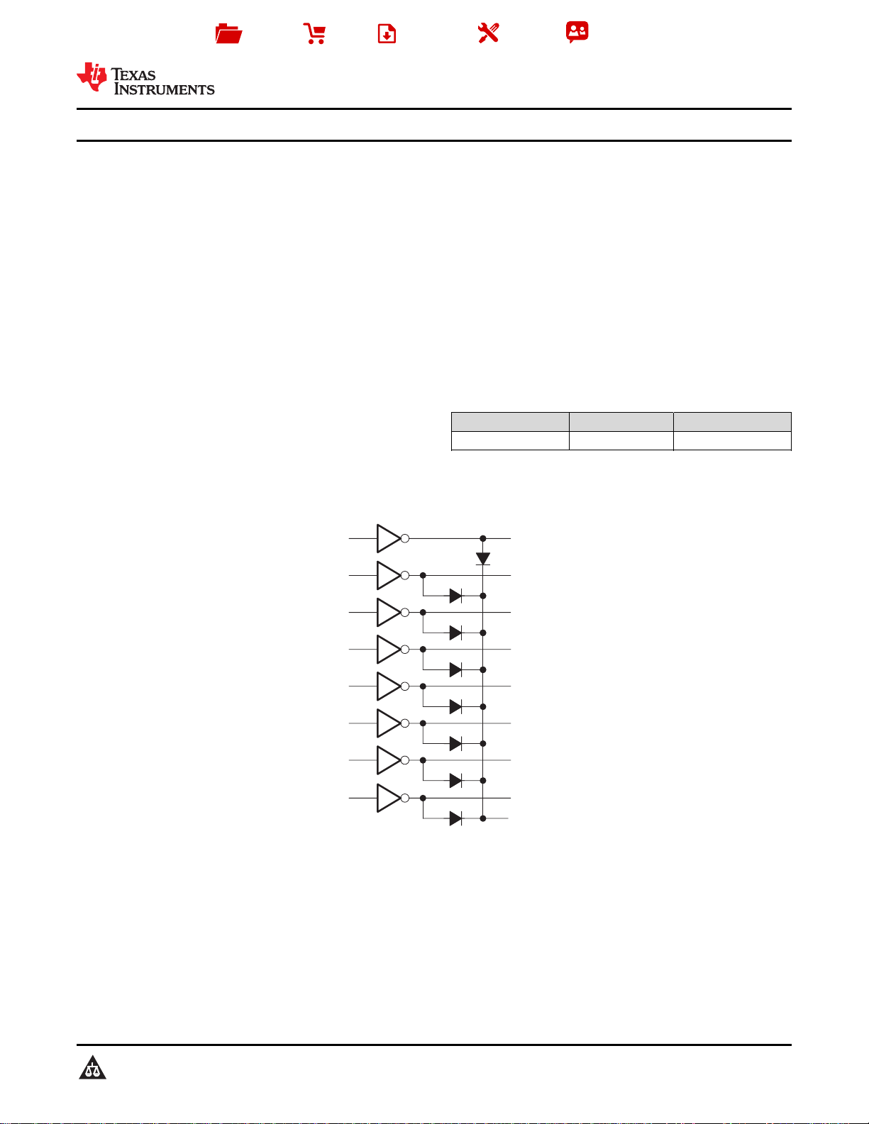
Logic Diagram
Device Information
the end of the data sheet.
(1)
1
An IMPORTANT NOTICE at the end of this data sheet addresses availability, warranty, changes, use in safety-critical applications,
intellectual property matters and other important disclaimers. PRODUCTION DATA.
Page 2

ULN2803A
SLRS049H –FEBRUARY 1997–REVISED FEBRUARY 2017
www.ti.com
Table of Contents
1 Features.................................................................. 1
2 Applications ........................................................... 1
3 Description ............................................................. 1
4 Revision History..................................................... 2
5 Pin Configuration and Functions......................... 3
6 Specifications......................................................... 4
6.1 Absolute Maximum Ratings...................................... 4
6.2 ESD Ratings.............................................................. 4
6.3 Recommended Operating Conditions....................... 4
6.4 Thermal Information.................................................. 4
6.5 Electrical Characteristics........................................... 5
6.6 Switching Characteristics.......................................... 5
6.7 Typical Characteristics.............................................. 5
7 Parameter Measurement Information .................. 6
8 Detailed Description.............................................. 9
8.1 Overview................................................................... 9
8.2 Functional Block Diagram......................................... 9
8.3 Feature Description................................................... 9
8.4 Device Functional Modes.......................................... 9
9 Application and Implementation ........................ 10
9.1 Application Information............................................ 10
9.2 Typical Application ................................................. 10
10 Power Supply Recommendations ..................... 12
11 Layout................................................................... 12
11.1 Layout Guidelines ................................................. 12
11.2 Layout Example .................................................... 12
12 Device and Documentation Support................. 13
12.1 Receiving Notification of Documentation Updates 13
12.2 Community Resources.......................................... 13
12.3 Trademarks........................................................... 13
12.4 Electrostatic Discharge Caution............................ 13
12.5 Glossary................................................................ 13
13 Mechanical, Packaging, and Orderable
Information........................................................... 13
4 Revision History
NOTE: Page numbers for previous revisions may differ from page numbers in the current version.
Changes from Revision G (January 2015) to Revision H Page
• Deleted obsolete orderable ULN2803AN and removed all references to N package............................................................ 1
• Added Storage temperature, T
• Deleted VIfrom Recommended Operating Conditions........................................................................................................... 4
• Added Ambient temperature, TAin Recommended Operating Conditions............................................................................. 4
• Changed coil supply voltage specifications in Design Parameters...................................................................................... 11
• Added Receiving Notification of Documentation Updates section and Community Resources section ............................. 13
in Absolute Maximum Ratings........................................................................................... 4
stg
Changes from Revision F (January 2014) to Revision G Page
• Added Applications, Device Information table, Pin Functions table, ESD Ratings table, Thermal Information table,
Typical Characteristics, Feature Description section, Device Functional Modes, Application and Implementation
section, Power Supply Recommendations section, Layout section, Device and Documentation Support section, and
Mechanical, Packaging, and Orderable Information section.................................................................................................. 1
Changes from Revision E (July 2006) to Revision F Page
• Updated document to new TI data sheet format - no specification changes. ........................................................................ 1
• Deleted Ordering Information table. ....................................................................................................................................... 1
2
Submit Documentation Feedback Copyright © 1997–2017, Texas Instruments Incorporated
Product Folder Links: ULN2803A
Page 3
11B 18 1C
22B 17 2C
33B 16 3C
44B 15 4C
55B 14 5C
66B 13 6C
77B 12 7C
88B 11 8C
9GND 10 COM
Not to scale
www.ti.com
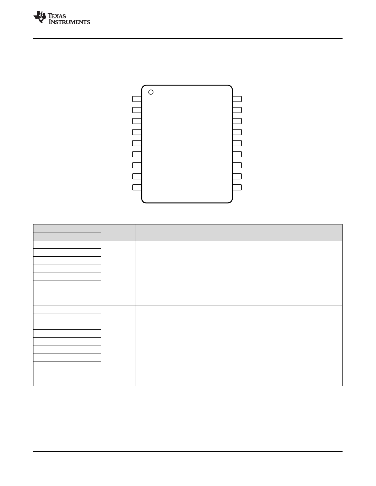
5 Pin Configuration and Functions
ULN2803A
SLRS049H –FEBRUARY 1997–REVISED FEBRUARY 2017
DW Package
18-Pin SOIC
Top View
Pin Functions
PIN
NAME NO.
1B 1
2B 2
3B 3
4B 4
5B 5
6B 6
7B 7
8B 8
1C 18
2C 17
3C 16
4C 15
5C 14
6C 13
7C 12
8C 11
GND 9 — Common emitter shared by all channels (typically tied to ground)
COM 10 I/O Common cathode node for flyback diodes (required for inductive loads)
TYPE DESCRIPTION
I Channel 1 through 8 Darlington base input
O Channel 1 through 8 Darlington collector output
Product Folder Links: ULN2803A
Submit Documentation FeedbackCopyright © 1997–2017, Texas Instruments Incorporated
3
Page 4
ULN2803A
SLRS049H –FEBRUARY 1997–REVISED FEBRUARY 2017
www.ti.com
6 Specifications
6.1 Absolute Maximum Ratings
at 25°C free-air temperature (unless otherwise noted)
V
CE
V
I
I(clamp) Output clamp current 500 mA
T
J
T
stg
(1) Stresses beyond those listed under Absolute Maximum Ratings may cause permanent damage to the device. These are stress ratings
(2) All voltage values, unless otherwise noted, are with respect to the emitter/substrate terminal GND.
Collector-emitter voltage 50 V
Input voltage
(2)
Peak collector current 500 mA
Total substrate-terminal current –2.5 A
Junction temperature –65 150 °C
Storage temperature –65 150 °C
only, which do not imply functional operation of the device at these or any other conditions beyond those indicated under Recommended
Operating Conditions. Exposure to absolute-maximum-rated conditions for extended periods may affect device reliability.
6.2 ESD Ratings
V
(ESD)
Electrostatic discharge
(1) JEDEC document JEP155 states that 500-V HBM allows safe manufacturing with a standard ESD control process.
(2) JEDEC document JEP157 states that 250-V CDM allows safe manufacturing with a standard ESD control process.
Human body model (HBM), per ANSI/ESDA/JEDEC JS-001
Charged device model (CDM), per JEDEC specification JESD22-C101
(1)
MIN MAX UNIT
30 V
VALUE UNIT
(1)
(2)
±2000
±500
V
6.3 Recommended Operating Conditions
over operating free-air temperature range (unless otherwise noted)
MIN MAX UNIT
V
CE
T
A
Collector-emitter voltage 0 50 V
Ambient temperature –40 85 °C
6.4 Thermal Information
ULN2803A
THERMAL METRIC
R
θJA
R
θJC(top)
R
θJB
ψ
JT
ψ
JB
R
θJC(bot)
Junction-to-ambient thermal resistance 66.4 °C/W
Junction-to-case (top) thermal resistance 29.5 °C/W
Junction-to-board thermal resistance 33.0 °C/W
Junction-to-top characterization parameter 6.0 °C/W
Junction-to-board characterization parameter 32.5 °C/W
Junction-to-case (bottom) thermal resistance N/A °C/W
(1) For more information about traditional and new thermal metrics, see the Semiconductor and IC Package Thermal Metrics application
report.
(1)
UNITDW (SOIC)
18 PINS
4
Submit Documentation Feedback Copyright © 1997–2017, Texas Instruments Incorporated
Product Folder Links: ULN2803A
Page 5
μ
μ
μ
μ
μ
μ
www.ti.com
6.5 Electrical Characteristics
at TA= 25°C free-air temperature (unless otherwise noted)
PARAMETER TEST CONDITIONS
I
CEX
I
I(off)
I
I(on)
V
I(on)
V
CE(sat)
I
R
V
F
C
i
Collector cutoff current
Off-state input current
Input current VI= 3.85 V, See Figure 5 0.93 1.35 mA
On-state input voltage
Collector-emitter saturation voltage
Clamp diode reverse current VR= 50 V, see Figure 8 50 μA
Clamp diode forward voltage IF= 350 mA see Figure 9 1.7 2 V
Input capacitance VI= 0, f = 1 MHz 15 25 pF
VCE= 50 V,
see Figure 3
VCE= 50 V,
TA= 70°C
VCE= 2 V,
see Figure 6
II= 250 μA,
see Figure 7
II= 350 μA,
see Figure 7
II= 500 μA,
see Figure 7
ULN2803A
SLRS049H –FEBRUARY 1997–REVISED FEBRUARY 2017
ULN2803A
MIN TYP MAX
II= 0 50 μA
IC= 500 μA,
see Figure 4
50 65 μA
IC= 200 mA 2.4
IC= 300 mA 3
IC= 100 mA 0.9 1.1
IC= 200 mA 1 1.3
IC= 350 mA 1.3 1.6
UNIT
VIC= 250 mA 2.7
V
6.6 Switching Characteristics
TA= 25°C
PARAMETER TEST CONDITIONS MIN TYP MAX UNIT
t
t
V
Propagation delay time, low- to high-level output
PLH
Propagation delay time, high- to low-level output 20
PHL
High-level output voltage after switching VS= 50 V, IO= 300 mA, see Figure 11 VS– 20 mV
OH
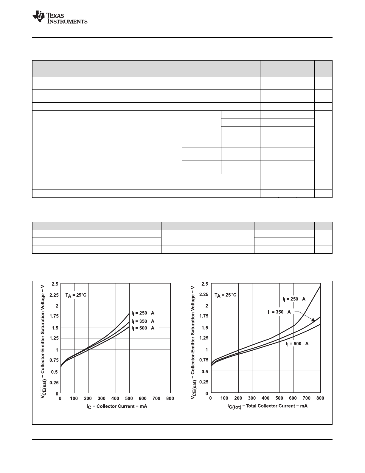
6.7 Typical Characteristics
VS= 50 V, CL= 15 pF, RL= 163 Ω,
See Figure 10
130
ns
Figure 1. Collector-Emitter Saturation Voltage vs Collector
Current (One Darlington)
Product Folder Links: ULN2803A
Figure 2. Collector-Emitter Saturation Voltage vs Total
Collector Current (Two Darlingtons in Parallel)
Submit Documentation FeedbackCopyright © 1997–2017, Texas Instruments Incorporated
5
Page 6
Open
V
F
I
F
Open
V
CE
I
C
I
I
hFE=
I
C
I
I
V
R
Open
I
R
Open
V
CE
I
C
V
I
Open
I
I
OpenV
I
Open V
CE
I
C
I
I(off)
Open V
CE
I
CEX
Open
ULN2803A
SLRS049H –FEBRUARY 1997–REVISED FEBRUARY 2017
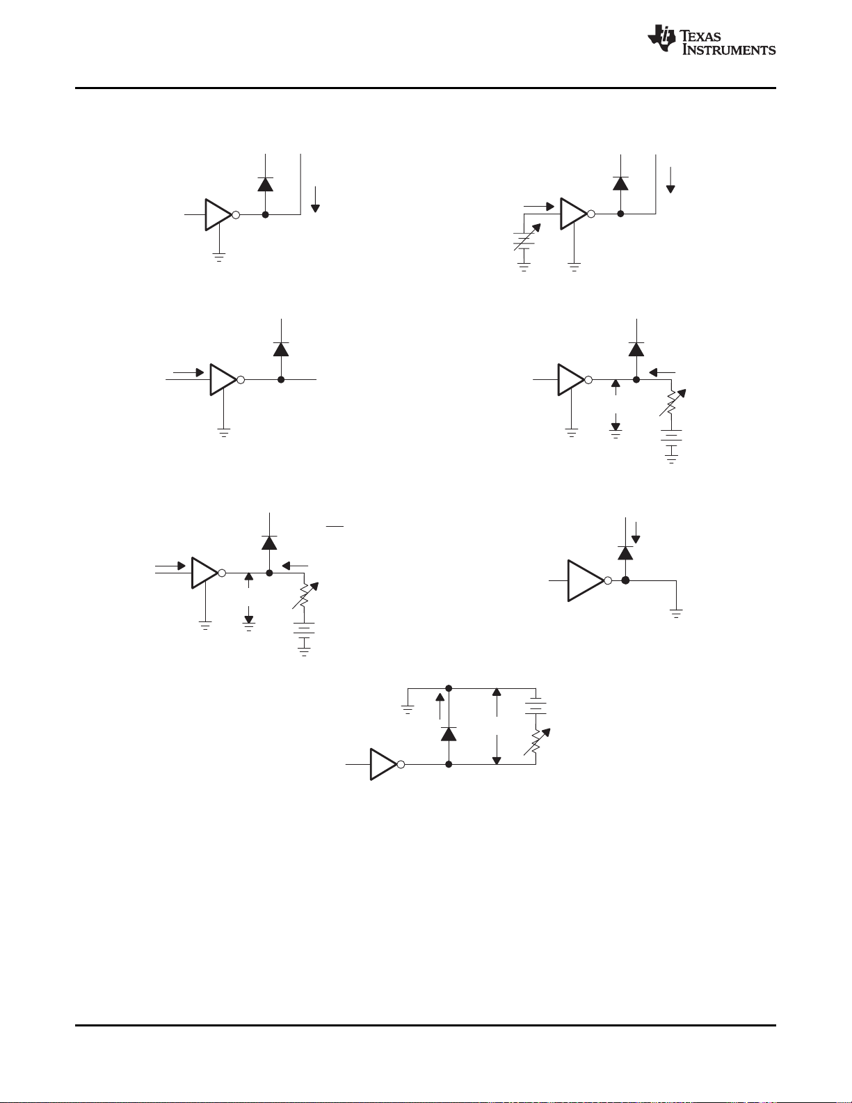
7 Parameter Measurement Information
www.ti.com
Figure 3. I
Figure 5. I
Figure 7. hFE, V
Test Circuit Figure 4. I
CEX
Test Circuit Figure 6. V
I(on)
Test Circuit Figure 8. IRTest Circuit
CE(sat)
Test Circuit
I(off)
Test Circuit
I(on)
Figure 9. VFTest Circuit
6
Submit Documentation Feedback Copyright © 1997–2017, Texas Instruments Incorporated
Product Folder Links: ULN2803A
Page 7
Pulse
Generator
(see Note A)
Input Open
VS= 50 V
RL= 163 Ω
CL= 15 pF
(see Note B)
Output
t
PHL
t
PLH
0.5 µs
<5 ns <10 ns
90%
50%
10% 10%
90%
50%
50% 50%
V
IH
(see Note C)
Input
Output
0
Test Circuit
Voltage Waveforms
V
OH
www.ti.com
ULN2803A
SLRS049H –FEBRUARY 1997–REVISED FEBRUARY 2017
Parameter Measurement Information (continued)
A. The pulse generator has the following characteristics: PRR = 12.5 kHz, ZO= 50 Ω.
B. CLincludes probe and jig capacitance.
C. VIH= 3 V
Figure 10. Propagation Delay Times
Product Folder Links: ULN2803A
Submit Documentation FeedbackCopyright © 1997–2017, Texas Instruments Incorporated
7
Page 8

Pulse
Generator
(see Note A)
Input
V
S
163 Ω
CL= 15 pF
(see Note B)
Output
40 µs
<5 ns <10 ns
90%
1.5 V
10% 10%
90%
1.5 V
V
IH
(see Note C)
Input
Output
0
2 mH
V
OH
Test Circuit
Voltage Waveforms
ULN2803A
SLRS049H –FEBRUARY 1997–REVISED FEBRUARY 2017
Parameter Measurement Information (continued)
www.ti.com
A. The pulse generator has the following characteristics: PRR = 12.5 kHz, ZO= 50 Ω.
B. CLincludes probe and jig capacitance.
C. VIH= 3 V
Figure 11. Latch-Up Test
8
Submit Documentation Feedback Copyright © 1997–2017, Texas Instruments Incorporated
Product Folder Links: ULN2803A
Page 9

2.7 kΩ
7.2 kΩ 3 kΩ
COM
Output C
E
Input B
ULN2803A
www.ti.com
SLRS049H –FEBRUARY 1997–REVISED FEBRUARY 2017
8 Detailed Description
8.1 Overview
This standard device has proven ubiquity and versatility across a wide range of applications. This is due to its
integration of 8 Darlington transistors that are capable of sinking up to 500 mA and wide GPIO range capability.
The ULN2803A is comprised of eight high voltage, high current NPN Darlington transistor pairs. All units feature
a common emitter and open collector outputs. To maximize their effectiveness, these units contain suppression
diodes for inductive loads. The ULN2803A has a series base resistor to each Darlington pair, thus allowing
operation directly with TTL or CMOS operating at supply voltages of 5 V or 3.3 V. The ULN2803A offers
solutions to a great many interface needs, including solenoids, relays, lamps, small motors, and LEDs.
Applications requiring sink currents beyond the capability of a single output may be accommodated by paralleling
the outputs.
8.2 Functional Block Diagram
8.3 Feature Description
Each channel of ULN2803A consists of Darlington connected NPN transistors. This connection creates the effect
of a single transistor with a very-high current gain. The very high β allows for high output current drive with a
very-low input current, essentially equating to operation with low GPIO voltages.
The GPIO voltage is converted to base current through the 2.7-kΩ resistor connected between the input and
base of the predriver Darlington NPN.
The diodes connected between the output and COM pin are used to suppress the kick-back voltage from an
inductive load that is excited when the NPN drivers are turned off (stop sinking) and the stored energy in the
coils causes a reverse current to flow into the coil supply through the kick-back diode.
In normal operation, the diodes on base and collector pins to emitter will be reverse biased. If these diode are
forward biased, internal parasitic NPN transistors will draw (a nearly equal) current from other (nearby) device
pins.
8.4 Device Functional Modes
8.4.1 Inductive Load Drive
When the COM pin is tied to the coil supply voltage, ULN2803A is able to drive inductive loads and suppress the
kick-back voltage through the internal free wheeling diodes.
8.4.2 Resistive Load Drive
When driving resistive loads, COM can be left unconnected or connected to the load voltage supply. If multiple
supplies are used, connect to the highest voltage supply.
Product Folder Links: ULN2803A
Submit Documentation FeedbackCopyright © 1997–2017, Texas Instruments Incorporated
9
Page 10

ULN2803A
IN3
IN4
OUT1
OUT2
OUT3
OUT4
IN5
IN6
IN7
GND
OUT5
OUT6
OUT7
COM
IN1
IN2
3.3 V Logic
VSUP
3.3 V Logic
3.3 V Logic
VSUP
IN8 OUT8
Copyright © 2017, Texas Instruments Incorporated
ULN2803A
SLRS049H –FEBRUARY 1997–REVISED FEBRUARY 2017
www.ti.com
9 Application and Implementation
NOTE
Information in the following applications sections is not part of the TI component
specification, and TI does not warrant its accuracy or completeness. TI’s customers are
responsible for determining suitability of components for their purposes. Customers should
validate and test their design implementation to confirm system functionality.
9.1 Application Information
ULN2803A will typically be used to drive a high voltage and/or current peripheral from an MCU or logic device
that cannot tolerate these conditions. The following design is a common application of ULN2803A, driving
inductive loads. This includes motors, solenoids, and relays. Each load type can be modeled by what is seen in
Figure 12.
9.2 Typical Application
10
Submit Documentation Feedback Copyright © 1997–2017, Texas Instruments Incorporated
Figure 12. ULN2803A as Inductive Load Driver
Product Folder Links: ULN2803A
Page 11

( )
J(MAX) A
(MAX)
JA
T TPD-
=
q
N
D OLi Li
i 1
P V I
=
= ´
å
ULN2803A
www.ti.com
SLRS049H –FEBRUARY 1997–REVISED FEBRUARY 2017
Typical Application (continued)
9.2.1 Design Requirements
For this design example, use the parameters listed in Table 1 as the input parameters.
Table 1. Design Parameters
DESIGN PARAMETER EXAMPLE VALUE
GPIO voltage 3.3 or 5 V
Coil supply voltage 12 to 50 V
Number of channels 8
Output current (R
Duty cycle 100%
9.2.2 Detailed Design Procedure
When using ULN2803A in a coil driving application, determine the following:
• Input voltage range
• Temperature range
• Output and drive current
• Power dissipation
9.2.2.1 Drive Current
The coil current is determined by the coil voltage (VSUP), coil resistance, and output low voltage (VOLor
V
CE(SAT)
I
COIL
).
= (V
SUP
– V
CE(SAT)
) / R
COIL
) 20 to 300 mA per channel
COIL
(1)
9.2.2.2 Output Low Voltage
The output low voltage (VOL) is the same thing as V
CE(SAT)
and can be determined by Figure 1, Figure 2, or
Electrical Characteristics.
9.2.2.3 Power Dissipation and Temperature
The number of coils driven is dependent on the coil current and on-chip power dissipation. To determine the
number of coils possible, use Equation 2 to calculate ULN2803A on-chip power dissipation PD.
where
• N is the number of channels active together.
• V
is the OUTipin voltage for the load current ILi. This is the same as V
OLi
CE(SAT)
(2)
To ensure the reliability of ULN2803A and the system, the on-chip power dissipation must be lower that or equal
to the maximum allowable power dissipation (PD) dictated by Equation 3.
where
• T
• TAis the operating ambient temperature.
• θJAis the package junction to ambient thermal resistance. (3)
is the target maximum junction temperature.
J(MAX)
TI recommends to limit ULN2803A IC’s die junction temperature to <125°C. The IC junction temperature is
directly proportional to the on-chip power dissipation.
Submit Documentation FeedbackCopyright © 1997–2017, Texas Instruments Incorporated
Product Folder Links: ULN2803A
11
Page 12

1
2
3
4
8
COM
7
6
5
16
GND
9
15
14
13
12
11
10
1B
2B
3B
4B
7B
6B
5B
1C
2C
3C
4C
7C
6C
5C
GND
8B
8C
18
17
Time (s)
Output voltage - V
-0.004 0 0.004 0.008 0.012 0.016
0
1
2
3
4
5
6
7
8
9
10
11
12
13
D001
Time (s)
Output voltage - V
-0.004 0 0.004 0.008 0.012 0.016
0
2
4
6
8
10
12
14
D001
ULN2803A
SLRS049H –FEBRUARY 1997–REVISED FEBRUARY 2017
9.2.3 Application Curves
The following curves were generated with ULN2803A driving an OMRON G5NB relay – Vin= 5.0 V; V
and R
COIL
= 2.8 kΩ
www.ti.com
= 12 V
sup
Figure 13. Output Response With Activation of Coil (Turn
On)
Figure 14. Output Response With De-Activation of Coil
(Turn Off)
10 Power Supply Recommendations
This part does not need a power supply; however, the COM pin is typically tied to the system power supply.
When this is the case, make sure that the output voltage does not heavily exceed the COM pin voltage. This will
heavily forward bias the flyback diodes and cause a large current to flow into COM, potentially damaging the onchip metal or overheating the part.
11 Layout
11.1 Layout Guidelines
Thin traces can be used on the input due to the low current logic that is typically used to drive ULN2803A. Take
care to separate the input channels as much as possible, as to eliminate crosstalk. TI recommends thick traces
for the output, in order to drive high currents as desired. Wire thickness can be determined by the trace
material's current density and desired drive current.
Because all of the channels currents return to a common emitter, it is best to size that trace width to be very
wide. Some applications require up to 2.5 A.
11.2 Layout Example
12
Submit Documentation Feedback Copyright © 1997–2017, Texas Instruments Incorporated
Figure 15. Package Layout
Product Folder Links: ULN2803A
Page 13

ULN2803A
www.ti.com
SLRS049H –FEBRUARY 1997–REVISED FEBRUARY 2017
12 Device and Documentation Support
12.1 Receiving Notification of Documentation Updates
To receive notification of documentation updates, navigate to the device product folder on ti.com. In the upper
right corner, click on Alert me to register and receive a weekly digest of any product information that has
changed. For change details, review the revision history included in any revised document.
12.2 Community Resources
The following links connect to TI community resources. Linked contents are provided "AS IS" by the respective
contributors. They do not constitute TI specifications and do not necessarily reflect TI's views; see TI's Terms of
Use.
TI E2E™ Online Community TI's Engineer-to-Engineer (E2E) Community. Created to foster collaboration
among engineers. At e2e.ti.com, you can ask questions, share knowledge, explore ideas and help
solve problems with fellow engineers.
Design Support TI's Design Support Quickly find helpful E2E forums along with design support tools and
contact information for technical support.
12.3 Trademarks
E2E is a trademark of Texas Instruments.
All other trademarks are the property of their respective owners.
12.4 Electrostatic Discharge Caution
This integrated circuit can be damaged by ESD. Texas Instruments recommends that all integrated circuits be handled with
appropriate precautions. Failure to observe proper handling and installation procedures can cause damage.
ESD damage can range from subtle performance degradation to complete device failure. Precision integrated circuits may be more
susceptible to damage because very small parametric changes could cause the device not to meet its published specifications.
12.5 Glossary
SLYZ022 — TI Glossary.
This glossary lists and explains terms, acronyms, and definitions.
13 Mechanical, Packaging, and Orderable Information
The following pages include mechanical, packaging, and orderable information. This information is the most
current data available for the designated devices. This data is subject to change without notice and revision of
this document. For browser-based versions of this data sheet, refer to the left-hand navigation.
Product Folder Links: ULN2803A
Submit Documentation FeedbackCopyright © 1997–2017, Texas Instruments Incorporated
13
Page 14

PACKAGE OPTION ADDENDUM
www.ti.com
PACKAGING INFORMATION
Orderable Device Status
ULN2803ADW ACTIVE SOIC DW 18 40 Green (RoHS
ULN2803ADWG4 ACTIVE SOIC DW 18 40 Green (RoHS
ULN2803ADWR ACTIVE SOIC DW 18 2000 Green (RoHS
ULN2803ADWRG4 ACTIVE SOIC DW 18 2000 Green (RoHS
(1)
The marketing status values are defined as follows:
ACTIVE: Product device recommended for new designs.
LIFEBUY: TI has announced that the device will be discontinued, and a lifetime-buy period is in effect.
NRND: Not recommended for new designs. Device is in production to support existing customers, but TI does not recommend using this part in a new design.
PREVIEW: Device has been announced but is not in production. Samples may or may not be available.
OBSOLETE: TI has discontinued the production of the device.
Package Type Package
(1)
Drawing
Pins Package
Qty
Eco Plan
(2)
& no Sb/Br)
& no Sb/Br)
& no Sb/Br)
& no Sb/Br)
Lead/Ball Finish
(6)
NIPDAU Level-2-260C-1 YEAR -40 to 85 ULN2803A
NIPDAU Level-2-260C-1 YEAR -40 to 85 ULN2803A
NIPDAU Level-2-260C-1 YEAR -40 to 85 ULN2803A
NIPDAU Level-2-260C-1 YEAR -40 to 85 ULN2803A
MSL Peak Temp
(3)
Op Temp (°C) Device Marking
(4/5)
(2)
RoHS: TI defines "RoHS" to mean semiconductor products that are compliant with the current EU RoHS requirements for all 10 RoHS substances, including the requirement that RoHS substance
do not exceed 0.1% by weight in homogeneous materials. Where designed to be soldered at high temperatures, "RoHS" products are suitable for use in specified lead-free processes. TI may
reference these types of products as "Pb-Free".
RoHS Exempt: TI defines "RoHS Exempt" to mean products that contain lead but are compliant with EU RoHS pursuant to a specific EU RoHS exemption.
Green: TI defines "Green" to mean the content of Chlorine (Cl) and Bromine (Br) based flame retardants meet JS709B low halogen requirements of <=1000ppm threshold. Antimony trioxide based
flame retardants must also meet the <=1000ppm threshold requirement.
(3)
MSL, Peak Temp. - The Moisture Sensitivity Level rating according to the JEDEC industry standard classifications, and peak solder temperature.
(4)
There may be additional marking, which relates to the logo, the lot trace code information, or the environmental category on the device.
(5)
Multiple Device Markings will be inside parentheses. Only one Device Marking contained in parentheses and separated by a "~" will appear on a device. If a line is indented then it is a continuation
of the previous line and the two combined represent the entire Device Marking for that device.
(6)
Lead/Ball Finish - Orderable Devices may have multiple material finish options. Finish options are separated by a vertical ruled line. Lead/Ball Finish values may wrap to two lines if the finish
value exceeds the maximum column width.
Important Information and Disclaimer:The information provided on this page represents TI's knowledge and belief as of the date that it is provided. TI bases its knowledge and belief on information
provided by third parties, and makes no representation or warranty as to the accuracy of such information. Efforts are underway to better integrate information from third parties. TI has taken and
6-Feb-2020
Samples
Addendum-Page 1
Page 15

PACKAGE OPTION ADDENDUM
www.ti.com
continues to take reasonable steps to provide representative and accurate information but may not have conducted destructive testing or chemical analysis on incoming materials and chemicals.
TI and TI suppliers consider certain information to be proprietary, and thus CAS numbers and other limited information may not be available for release.
In no event shall TI's liability arising out of such information exceed the total purchase price of the TI part(s) at issue in this document sold by TI to Customer on an annual basis.
6-Feb-2020
Addendum-Page 2
Page 16

PACKAGE MATERIALS INFORMATION
www.ti.com 14-Jun-2019
TAPE AND REEL INFORMATION
*All dimensions are nominal
Device Package
Type
ULN2803ADWR SOIC DW 18 2000 330.0 24.4 10.9 12.0 2.7 12.0 24.0 Q1
Package
Drawing
Pins SPQ Reel
Diameter
(mm)
Reel
Width
W1 (mm)
A0
(mm)B0(mm)K0(mm)P1(mm)W(mm)
Pin1
Quadrant
Pack Materials-Page 1
Page 17

PACKAGE MATERIALS INFORMATION
www.ti.com 14-Jun-2019
*All dimensions are nominal
Device Package Type Package Drawing Pins SPQ Length (mm) Width (mm) Height (mm)
ULN2803ADWR SOIC DW 18 2000 370.0 355.0 55.0
Pack Materials-Page 2
Page 18

Page 19

Page 20

Page 21

IMPORTANT NOTICE AND DISCLAIMER
TI PROVIDES TECHNICAL AND RELIABILITY DATA (INCLUDING DATASHEETS), DESIGN RESOURCES (INCLUDING REFERENCE
DESIGNS), APPLICATION OR OTHER DESIGN ADVICE, WEB TOOLS, SAFETY INFORMATION, AND OTHER RESOURCES “AS IS”
AND WITH ALL FAULTS, AND DISCLAIMS ALL WARRANTIES, EXPRESS AND IMPLIED, INCLUDING WITHOUT LIMITATION ANY
IMPLIED WARRANTIES OF MERCHANTABILITY, FITNESS FOR A PARTICULAR PURPOSE OR NON-INFRINGEMENT OF THIRD
PARTY INTELLECTUAL PROPERTY RIGHTS.
These resources are intended for skilled developers designing with TI products. You are solely responsible for (1) selecting the appropriate
TI products for your application, (2) designing, validating and testing your application, and (3) ensuring your application meets applicable
standards, and any other safety, security, or other requirements. These resources are subject to change without notice. TI grants you
permission to use these resources only for development of an application that uses the TI products described in the resource. Other
reproduction and display of these resources is prohibited. No license is granted to any other TI intellectual property right or to any third
party intellectual property right. TI disclaims responsibility for, and you will fully indemnify TI and its representatives against, any claims,
damages, costs, losses, and liabilities arising out of your use of these resources.
TI’s products are provided subject to TI’s Terms of Sale (www.ti.com/legal/termsofsale.html) or other applicable terms available either on
ti.com or provided in conjunction with such TI products. TI’s provision of these resources does not expand or otherwise alter TI’s applicable
warranties or warranty disclaimers for TI products.
Mailing Address: Texas Instruments, Post Office Box 655303, Dallas, Texas 75265
Copyright © 2020, Texas Instruments Incorporated
 Loading...