

Texas Instruments UCC39422PWTR, UCC39422PW, UCC39422N, UCC39421PWTR, UCC39421PW Datasheet
...
UCC29421/2
T
UCC39421/2
Multimode High Frequency PWM Controller
FEATURES
Operation Down to an Input Voltage
•
of 1.8V
High Efficiency Boost or Flyback
•
(Buck-Boost) Topologies
Drives External FETs for High Current
•
Applications
Up to 2MHz Oscillator
•
Synchronizable Fixed Frequency
•
Operation
High Efficiency Low Power Mode
•
High Efficiency at Very Low Power
•
with Programmable Variable
Frequency Mode
• Pulse by Pulse Current Limit
• 5µA Supply Current in Shutdown
• 150µA Supply Current in Sleep Mode
• Selectable NMOS or PMOS
Rectification
• Built-in Power on Reset
(UCC39422 Only)
• Built-in Low Voltage Detect
(UCC39422 Only)
SIMPLIFIED BLOCK DIAGRAM AND APPLICATION CIRCUIT
1.8VMIN
97
1.25V
VREF
SYNC/SD
RT
GND
RESET
LOWBAT
13
14
PWM CIRCUITRY
CURRENT LIMIT
LOW POWER
COMPENSATION
15
1
10
PWM
OSC
MODE
SLOPE
PFM MODE
CONTROL
LP_MODE
ANTI-
CROSS
COND.
200mS
RESET/
POR
CHARGE
PUMP
VGD
X10
ERROR
AMP
1.23/1.25V
UCC39422
ONLY
+
–
VPUMP
+
–
1.25V
+
–
–
+
–
+
1.25V
VINVPUMP
1.18V
19
12
17
18
16
20
11
8
3
2
4
6
5
CP
VOUT
RSEN
RECT
RSEL
CHRG
ISENSE
PGND
FB
COMP
PFM
RSADJ
VDET
PRELIMINARY
+
2CELL
ALKALINE/
NiCd OR
+
1 LI-ION
50mV TYP
VOU
UDG-98122
DESCRIPTION
The UCC39421 family of synchronous PWM controllers
is optimized to operate from dual Alkaline/NiCd cells or a
single Lithium-Ion (Li-Ion) cell, and convert to adjustable
output voltages from 2.5V to 8V. For applications where
the input voltage does not exceed the output, a standard
boost configuration is utilized. For other applications
where the input voltage can swing above and below the
output, a 1:1 coupled-inductor (Flyback or SEPIC) is
used in place of the single inductor. Fixed frequency op
eration can be programmed, or synchronized to an exter
nal clock source. In applications where at light loads
variable frequency mode is acceptable, the IC can be
programmed to automatically enter PFM (Pulse Fre
quency Modulation) mode for an additional efficiency
benefit.
SLUS246A - OCTOBER 1999
Synchronous rectification provides excellent efficiency at
high power levels, where N or P type MOSFETs can be
used. At lower power levels (10-20% of full load) where
fixed frequency operation is required, Low Power Mode
is entered. This mode optimizes efficiency by cutting
back on the gate drive of the charging FET. At very low
power levels, the IC enters a variable frequency mode
(PFM). PFM can be disabled by the user.
-
Other features include pulse by pulse current limiting,
-
and a low 5µA quiescent current during shutdown. The
UCC39422 incorporates programmable Power on Reset
circuitry and an uncommitted comparator for low voltage
-
detection. The available packages are 20 pin TSSOP, or
20 pin N for the UCC39422, and 16 pin TSSOP, or 16
pin N for the UCC39421.
UCC29421/2
UCC39421/2
ABSOLUTE MAXIMUM RATINGS
Supply Voltage (VIN, VOUT,VPUMP) . . . . . . . . . . . . . . . . . . 8V
CP . . . . . . . . . . . . . . . . . . . . . . . . . . . . . . . . . . . . . . . . . . . . . 8V
RSEN. . . . . . . . . . . . . . . . . . . . . . . . . . . . . . . . . . . . –0.3 to 12V
SYNC/SD. . . . . . . . . . . . . . . . . . . . . . . . . . . . . . . . . . –0.3 to 5V
ISENSE . . . . . . . . . . . . . . . . . . . . . . . . . . . . . . . . . . . –0.3 to 1V
Storage Temperature . . . . . . . . . . . . . . . . . . . –65°C to +150°C
Junction Temperature. . . . . . . . . . . . . . . . . . . –55°C to +150°C
Lead Temperature (Soldering, 10 sec.) . . . . . . . . . . . . . +300°C
All voltages are with respect to GND. Currents are positive
into, negative out of the specified terminal. Consult Packaging
Section of Databook for thermal limitations and considerations
of packages.
TSSOP-16, DIL-16 (TOP VIEW)
N, PW Packages
RSEN
VOUT
RECT
PGND
1
2
3
4
RSEL16
15
COMP
FB
14
PFM
13
CONNECTION DIAGRAMS
TSSOP-20, DIL-20 (TOP VIEW)
N, PW Packages
RESETB
RSEN
VOUT
RECT
PGND
CHRG
VPUMP
LOWBAT
1
2
3
4
5
6
7
8
CP
VIN ISENSE
9
10 VDET
20
19
18
17
16
15
14
13
12
11
RSADJ
RSEL
COMP
FB
PFM
GND
RT
SYNC/SD
CHRG
VPUMP
CP
VIN
5
6
7
8
ELECTRICAL CHARACTERISTICS: Unless otherwise stated these specifications apply for T
UCC29421/2, 0°C to +70°C for UCC39421/2; R
12
11
10
9
GND
RT
SYNC/SD
ISENSE
=100K, V
T
VPUMP
=6V, V
VIN
=3V
= –40°C to +85°C for
A
PARAMETER TEST CONDITIONS MIN MAX UNITS
VIN Section
Minimum Start-up Voltage 1.5 1.8 V
Operating Current Not in PFM Mode, No Load 35 60
Sleep Mode Current PFM Mode, No Load 35 60
Shutdown Supply Current SYNC/SD = High 1.5 4
Startup Frequency V
Startup Off Time V
Startup CS Threshold V
Minimum PUMP or VOUT Voltage to Exit
= 1.8V 60 120 190 kHz
IN
= 1.8V 2 5 s
IN
= 1.8V 36 56 mV
IN
2.2 2.5 2.8 V
Startup
VPUMP Section
Regulation Voltage V
=3.3V 5.5 6.6 V
VOUT
Operating Current Outputs OFF 100 275
Sleep Mode Current 515
Shutdown Supply Current SYNC/SD = High, V
CP Voltage to Turn On Pump Switch V
Pump Switch RDS
ON
= 5V 5.3 5.5 V
VPUMP
OUT
= 3V, V
= 3V 2 15 A
VPUMP
4
A
A
A
A
A
2
UCC29421/2
UCC39421/2
ELECTRICAL CHARACTERISTICS:
UCC29421/2, 0°C to +70°C for UCC39421/2; R
Unless otherwise stated these specifications apply for TA= –40°C to +85°C for
=100K, V
T
VPUMP
=6V, V
VIN
=3V
PARAMETER TEST CONDITIONS MIN MAX UNITS
VOUT Section
Operating Current 500 650
Sleep Mode Current 50 100 150
Shutdown Supply Current SYNC/SD = High 1 2.2
V
PUMP
to V
Threshold to Enable
OUT
V
= 3.3V 1.4 1.7 2.0 V
OUT
N-Channel Rectifier
Error Amp Section
Regulation Voltage 2V < VIN < 5V 1.21 1.24 1.27 V
FB Input Current V
Max Sinking Current, I
Max Sourcing Current, I
OL
OH
Transconductance V
Unity Gain Bandwidth C
Max Output Voltage V
= 1.25V 100 350 nA
FB
V
= 1V, VFB= Regulation Voltage +50mV 6.5 13 20 A
COMP
V
= 0V, VFB= Regulation Voltage –50mV –20 –13 –6.5 A
COMP
= Regulation Voltage ±4mV 150 270 370 S
FB
= 330pF 100 kHz
C
= 0V 1.9 2.3 V
FB
Oscillator Section
Frequency Stability R
= 350k 100 150 190 kHz
T
= 100k 375 475 575 kHz
R
T
= 35k 0.9 1.2 1.4 MHz
R
T
RT Voltage 0.600 0.625 0.650 V
SYNC Threshold 0.9 1.2 1.6 V
SYNC Input Current SYNC/SD = 2.5V 200 nA
Max SYNC High Time To Avoid Shutdown 11 20 29
SYNC Range R
= 100k 1.1ƒo 1.5ƒo kHz
T
Current Sense Section
Gain 8 10 11 V/V
Overcurrent Limit Threshold 150 200 mV
Unity Gain Bandwidth 25 MHz
COMP Voltage to I
Accuracy I
SENSE
= 70mV 0.8 1.0 1.2 V
SENSE
PWM Section
Maximum Duty Cycle V
Minimum Duty Cycle V
Low Power Mode V
Threshold At COMP pin 0.5 0.6 0.7 V
COMP
Slope Compensation Accuracy R
= 0V, VFB = 0V 80 88 %
ISENSE
= 1.5V 0 %
FB
= 350k, R
T
= 20k 1.4 2.8 4.0 A/s
SLOPE
Rectifier Zero Current Threshold RSEL = GND –2 15 28 mV
RSEL = VIN –28 –15 2 mV
RSEL Threshold 0.5 0.9 1.3 V
PFM Section
PFM Disable Threshold 0.17 0.22 0.27 V
Comp Hold During Sleep V
Startup Delay After Sleep V
= 0.4 0.45 V
PFM
< 1.23V 4 9 s
FB
FB Voltage to Sleep Off 1.19 1.22 1.25 V
FB Voltage to Sleep On 1.22 1.25 1.28 V
Low Power Mode Timer After Sleep 250 450 µs
A
A
A
s
3
UCC29421/2
UCC39421/2
ELECTRICAL CHARACTERISTICS:
UCC29421/2, 0°C to +70°C for UCC39421/2; R
PARAMETER TEST CONDITIONS MIN MAX UNITS
VGSW Drive Section
Rise Time C
Fall Time C
Output High I
Output Low I
Charge Off to Rectifier On Delay 10 30 50 ns
RECT Drive Section
Rise Time C
Fall Time C
Output High I
Output Low Rectifier I
Rectifier Off to Charge On Delay 10 20 50 ns
RESET Section (UCC39422 Only)
Reset Timeout C
Reset Threshold % Below Regulation Voltage –7 –5.5 –4 %
Output Low Voltage Reset Condition, I = 5mA 0.1 0.25 V
Output Leakage RESET = 8V 0.05 0.2
Voltage Detection Section (UCC39422 Only)
Threshold Voltage 1.18 1.26 1.34 V
Output Low Voltage I = 5mA 0.15 0.3 V
Output Leakage LOWBAT = 8V 0.05 0.25
Unless otherwise stated these specifications apply for TA= –40°C to +85°C for
=100K, V
T
= 1nF 18 35 ns
O
= 1nF 14 30 ns
O
= –100mA, Respect to VPUMP 0.4 0.65 V
OUT
= –1mA, Respect to VPUMP 4 10 mV
I
OUT
= 100mA 0.2 0.35 V
OUT
= 1mA 2 6 mV
I
OUT
= 1nF 20 40 ns
O
= 1nF 14 30 ns
O
= –100mA, Respect to VPUMP 0.2 0.5 V
OUT
= –1mA, Respect to VPUMP 5 10 mV
I
OUT
= 100mA 0.2 0.35 V
OUT
= 1mA 2 6 mV
I
OUT
= 0.33 F 100 250 400 ms
RSADJ
VPUMP
=6V, V
VIN
=3V
A
A
PIN DESCRIPTIONS
COMP: This is the output of the transconductance error
amplifier. Connect the compensation components from
this pin to ground.
CHRG: This is the gate drive output for the N-channel
charge MOSFET. Connect it to the gate directly, or
through a low value gate resistor.
CP: This is the input for the charge pump. For
applications requiring a charge pump, connect this pin to
the charge pump diode and flying capacitor, as shown in
the applications diagram of Fig 5. For applications where
no charge pump is required, this pin should be grounded.
FB: The feedback input is the inverting input to the tran
sconductance error amplifier. Connect this pin to a
resistive divider between V
voltage will be regulated to:
and ground. The output
OUT
R
V
OUT
=•
125
.
1
RR
+
12
()
where R1 goes to GND and R2 goes to VOUT.
GND: This is the signal ground pin for the device. It
should be tied to the local ground plane.
ISENSE: This is the input to the X10 wide bandwidth
current sense amplifier. Connect this pin to the high side
of the current sense resistor. An internal current is
sourced out this pin for slope compensation. For
applications requiring slope compensation (or filtering of
the current sense signal), use a resistor in series with
this pin.
LOWBAT: This is the open drain output of the
uncommitted comparator. (UCC39422 only). This output
is low when the VDET pin is above 1.25V.
4

PIN DESCRIPTIONS (cont.)
PFM: This is the programming pin for the PFM (Pulse
Frequency Modulation) Mode threshold. Connect this pin
to a resistive divider off of the FB pin (or VOUT) to set the
PFM threshold. To disable PFM Mode, connect this pin to
ground (below 0.2V).
PGND: This is the power ground pin for the device.
Connect it directly to the ground return of the current
sense resistor.
RECT: This is the gate drive output for the synchronous
rectifier. Connect it to the gate of the P or N channel
MOSFET directly, or through a low value gate resistor.
RECTSEN: This pin is used to sense the voltage across
the synchronous rectifier for commutation. In boost
configurations, connect this pin through a 1K resistor to
the junction of the two MOSFETs and the inductor. In
flyback and SEPIC configurations, connect this pin
through a 1K resistor to the junction of the drain of the
synchronous rectifier and the secondary side winding of
the coupled inductor.
RSADJ: A capacitor from this pin to ground sets the
reset delay. (UCC39422 only)
RSEL: This pin programs the device for N channel or P
channel synchronous rectifiers by inverting the phase of
the RECT gate drive output. Connect this pin to ground
for N-channel MOSFETs, connect it to V
MOSFETs.
RESET:
This is the open drain output of the Reset
comparator. (UCC39422 only) and is active low.
for P-channel
IN
UCC29421/2
UCC39421/2
RT: A resistor from this pin to ground programs the
frequency of the pulse width modulator.
SYNC/SD: This dual function pin is the SYNC and
Shutdown input. To synchronize the internal clock to an
external source, this pin must be driven above 2.0V. The
clock syncs to the rising edge of the input. To shutdown
the converter, this pin must be held high (above 2.0V) for
a minimum of 20
grounded.
VPUMP: This is the output of the charge pump. For
applications requiring a charge pump, connect a 1
capacitor from this pin to ground. Otherwise, connect
this pin to the higher of V
0.1µF capacitor.
VOUT: Connect this pin to the output voltage. This input
is used for sensing the voltage across the synchronous
rectifier and for bootstrapping the gate drive to the
charge FET and should be decoupled with a 0.1µF
capacitor.
VIN: This is the input power pin of the device. Connect
this pin to the input voltage source. A 0.1
capacitor should be connected between this pin and
ground.
VDET: This is the non-inverting input to an uncommitted
comparator. This input may be used for detecting a low
battery condition. (UCC39422 only)
sec. If not used, this pin should be
or V
IN
, and decouple with a
OUT
F decoupling
F
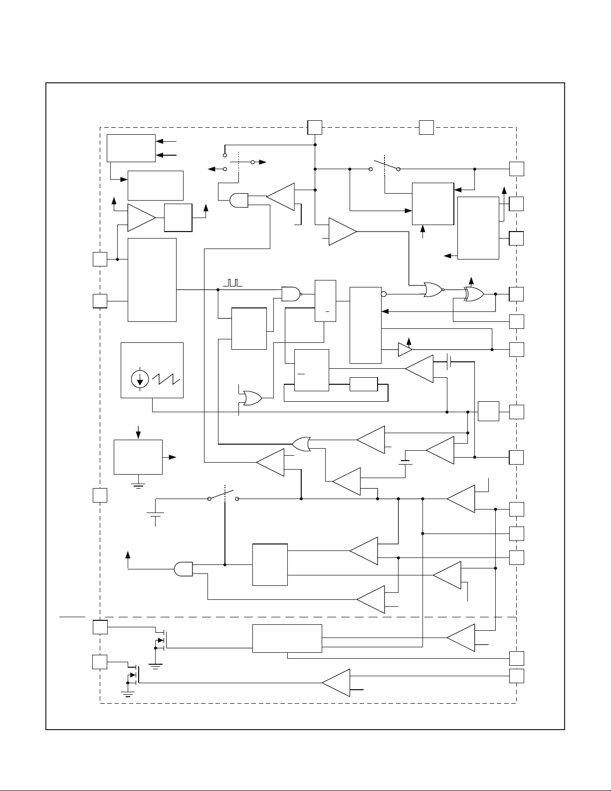
APPLICATION INFORMATION
The UCC39421 is a high frequency, synchronous PWM
controller optimized for portable, battery powered appli
cations where size and efficiency are of critical impor
tance. It includes high speed, high current FET drivers
for those converter applications requiring low RDS
ternal MOSFETs. A detailed block diagram is shown in
Fig 1.
Optimizing Efficiency
The UCC39421 optimizes efficiency, extending battery
life, by its low quiescent current and its synchronous rec
tifier topology. The additional features of Low Power
Mode and PFM Mode maintain high efficiency over a
wide range of load current. These features will be dis
cussed in detail.
ON
ex
Power Saving Modes
Since this is a peak current mode controller, the error
amplifier output voltage sets the peak inductor current re
quired to sustain the load. The UCC39421 incorporates
two special modes of operation designed to optimize effi
ciency over a wide range of load current. This is done by
comparing the error amplifier output voltage (on the
COMP pin) to two fixed thresholds (one of which is user
programmable). If the error amplifier output voltage drops
below the first threshold, Low Power (LP) mode will be
entered. If the error amplifier output voltage drops even
further, below a second user programmable threshold,
PFM Mode will be entered. These modes of operation
are designed to maintain high efficiency at light load, and
are described in detail below. Refer to the simplified
block diagram of Fig. 2 for the control logic.
5
-
-
APPLICATION INFORMATION (cont.)
VPUMP
VOUT
VIN
1=SD
20uS
DELAY
85%
DMAX
CLK
VPUMP >2.5V
SYNC/SD
RT
1.25V
13
14
VDD
CONTROL
VDD
VDD BIAS
CONTROL
AND UVLO
–
+
SLOPECOMP
PWM
OSC
UCC29421/2
UCC39421/2
VINVPUMP
7 9
VGD
+
–
VIN
VOUT+2V
R
Q
S
QQR
QQR
MUX
A
B
A/B
S
S
–
+
ANTI-
CROSS
COND.
START-UP
2.5µS
CONTROL
VGD
PUMP
SWITCH
VIN
IZERO
–
+
ADAPTIVE
CURRENT
SENSING
VPUMP
36mV
+
PGND
ZERO
19
CP
8
VOUT
3
RSEN
2
RECT
4
RSEL
CHRG
6
GND
RESET
LOWBAT
V
IN
1.25V
VREF
15
1=SLEEP
SLEEP=
POWER DOWN ALL
BUTVOUTCOMP
1
10
+
PFM
10-20% OF FULL
LOAD=LP_MODE
50mV
UCC29422
ONLY
VOUT>2.5V
LP_MODE
Q
+
0.5V
–
S
R
RESET/POR
ILIM COMP
PWM
COMP
+
–
PFM DISABLE
COMP
+
–
+
–
–
+
+
–
1.25V
0.15V
+
ERROR AMP
0.2V
30MHz AMP
+
X10
0.3V
–
+
–
+
–
1.23/1.25
–
+
LEB
1.25V
1.18V
12
17
18
16
20
11
5
ISENSE
PGND
FB
COMP
PFM
RSADJ
VDET
Figure 1. Detailed block diagram.
UDG-98107
6
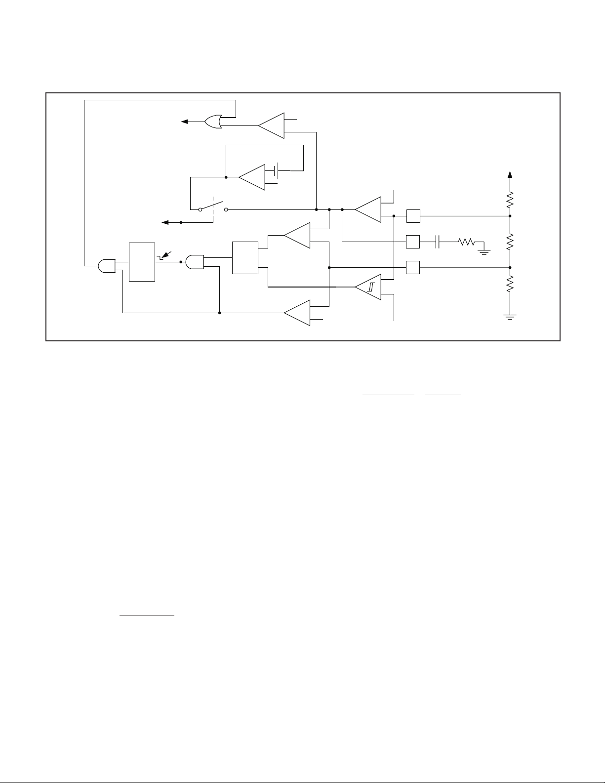
APPLICATION INFORMATION (cont.)
LP_MODE
LPM COMP
+
–
UCC29421/2
UCC39421/2
0.5V
50mV
+
–
+
1=SLEEP
200µs
ONE
SHOT
HOLD AMP
PFM
PFM COMP
S
Q
R
PFM DISABLE COMP
–
+
+
–
ERROR AMP
0.2V
+
–
–
+
1.25V
FB
COMP
PFM
1.23/1.25
Figure 2. Simplified block diagram of Low Power and Pulse Mode control logic.
−
05 03
..
Low Power Mode
During normal operation, at medium to high load cur-
I
PEAK
()
=
KR R
•
SENSE SENSE
=
rents, the switching frequency remains fixed, programmed by the resistor on the RT pin. At these higher
loads, the gate drive output on the CHRG pin (for the N
channel charge FET) will be the higher of V
or V
IN
PUMP
When the load current drops (sensed by a drop in the er
ror amp voltage), the UCC39421 will automatically enter
LP mode, and the gate drive voltage on the CHRG pin
will be reduced to lower gate drive losses. This helps to
maintain high efficiency at light loads where the gate
drive losses begin to dominate and the lowest possible
Rdson is not required. If the load increases, normal or
“High Power” mode will resume. The expression for gate
drive power loss is given by equation 1. It can be seen
that the power varies as a function of the applied gate
voltage squared.
2
••
GG
V
S
P
GATELOSS
QV f
=
Where 0.5V is the threshold for LP mode, 0.3V is the internal offset and K is the nominal current sense amplifier
gain of 10 and R
.
resistor. If the peak inductor current is below this value,
-
SENSE
is the value of the current sense
the UCC39421 will enter LP mode and the gate drive
voltage on the CHRG pin will be equal to V
currents higher than this, the gate drive voltage will be
the higher of V
or VPUMP.
IN
PFM Mode
At very light loads, the UCC39421 will enter PFM Mode.
In this mode, when the error amplifier output voltage
drops below the PFM threshold, the controller goes into
sleep mode until V
has dropped slightly (20mV mea
OUT
sured at the feedback pin). At this time, the controller will
(1)
turn back on and operate at fixed frequency for a short
duration (typically a few hundred microseconds) until the
output voltage has increased and the error amplifier out
put voltage has dropped below the PFM threshold once
Where Q
is the total gate charge and Vsis the gate volt
g
age specified in the MOSFET manufacturer’s data sheet,
is the applied gate drive voltage, and f is the switching
V
g
frequency.
The nominal COMP voltage where LP mode will be en
tered is 0.5V. Given the internal offset and gain of the
current sense amplifier, this corresponds to a peak
again. Then the converter will turn off and the cycle will
repeat. This results in a very low duty cycle of operation,
reducing all losses and greatly improving light load effi
ciency. During sleep mode, most of the circuitry internal
to the UCC39421 is powered down, reducing quiescent
current and maximizing efficiency.
switch current of:
002
.
VOUT
SENSE
in
UDG-98108
(2)
. At peak
-
-
-
7

APPLICATION INFORMATION (cont.)
The peak inductor current at which this mode will be en
tered is user programmable, by setting the voltage on the
PFM pin. This can be done with a single resistor in series
with the feedback divider, as shown in the application di
agrams. The nominal peak current threshold for PM
mode will be defined by:
(3)
is the
I
PEAK
125 1
12
RR
()
≅
KR
+
•
R
•
SENSE
−
03..
Where 0.3V is the internal offset and K is the nominal
current sense amplifier gain of 10 and R
SENSE
value of the current sense resistor. Note that in this case,
the PFM pin voltage is set by the R1/R2 resistive divider
off of the FB pin, which is regulated to 1.25V.
To further increase efficiency in Pulse mode, the gate
drive on the CHRG pin will be held in the LP mode for
sec each time the controller comes on. This keeps
200
gate drive losses low, even though the error amplifier
output voltage may overshoot slightly when coming out
of PFM. During sleep mode, the COMP pin is forced to
50mV above the PFM pin voltage. This minimizes error
amplifier overshoot when coming out of sleep mode, and
prevents erroneously tripping the PFM comparator.
Disabling PFM Mode
The user may disable PFM mode by pulling the PFM pin
below 0.2V. In this case, the UCC39421 will remain on,
in fixed frequency operation at all load currents. The
PFM pin can also be driven, through a resistive divider,
off of an output from the system controller. This allows
the system controller to prepare for an expected step in
crease in load, improving the converter’s large signal
transient response. An example of this is shown in Fig 3.
Choosing a Topology and Optimal Synchronous
Rectifier
The UCC39421 is designed to be very flexible, and can
be used in Boost, Flyback and SEPIC topologies. It can
operate from input voltages between 1.8 and 8.0V. Out
put voltages can be between 2.5V and 8.0V. (Note that
at higher input voltages, such as from four or five Alka
line or Nickel cells or two Li-ion cells, a buck regulator
UCC29421/2
UCC39421/2
-
UCC39421
-
PFM
Figure 3. Driving the PFM pin from a controller
output.
would usually be employed.) It will also drive either
N-channel or P-channel MOSFET synchronous rectifiers.
Table 1 can be used to select the appropriate topology
for a given combination of input and output voltage re
quirements. Although it is designed to operate as a peak
current mode controller, it can also be configured for volt
age mode control. This will be discussed in a later section.
The user can program the gate drive output on the RECT
pin for N-channel MOSFETs by grounding the RSEL pin,
or for P-channel MOSFETs by connecting the RESEL
pin to VIN. Table 2 is used to determine whether an N or
P channel synchronous rectifier should be used.
Note: In all cases, low voltage logic MOSFETs should be
used to achieve the lowest possible on-resistance for the
highest efficiency
.
The application diagrams in Figs 4-8 illustrate the use of
the UCC39421 in all the topologies, using N and P chan
nel rectifiers. They will be discussed in detail in the next
section.
Note that the higher the frequency of operation, the more
critical the MOSFET gate charge becomes for efficiency,
particularly at light loads. However, high load currents
demand lower RDS
, which will tend to increase gate
ON
charge. These two parameters should be balanced. At
lower frequencies, the gate charge will become less im
portant, at 1MHz or more, it is critical.
-
-
ENABLE OUTPUT
FROM CONTROLLER
R2
7
R1
-
-
-
-
Table I. Selecting Topology Based on Input and Output Voltage Requirements
Cell Type No. of Cells VINRange V
Alkaline or NiCd, NiMH 2 1.8V -3.0V 3.0 < V < 8.0 Boost
3 2.7V - 4.5V 2.5 < V < 3.9 Flyback or SEPIC
4.5 < V < 8.0 Boost
Li-Ion 1 2.3V - 4.2V 2.5 < V < 3.6 Flyback or SEPIC
4.2 < V < 8.0 Boost
OUT
Topology
8

APPLICATION INFORMATION (cont.)
Boost Topology
The boost topology is simple and efficient, and should be
used whenever the desired output voltage is greater than
the maximum input voltage.
Boost Using Two N-Channel MOSFETs
A boost converter using two N-channel MOSFETs is
shown in Fig 4. This configuration is optimal for output
voltages below 4V, where the output voltage may not be
high enough to provide optimal gate drive for a
P-channel MOSFET. Note that in this case, a charge
pump is required to provide proper gate drive levels. This
Table II. Selecting Synchronous Rectifier Based on Topology and Output Voltage
Topology VOUT Synchronous Rectifier
Boost 3.0 < V < 8.0 P-channel (low voltage logic)
V < 4.0 N-channel (low voltage logic)
Note: Requires a diode and a capacitor for the charge pump
Flyback 2.5 < V < 3.0 N-channel (low voltage logic)
Note: Requires a diode and a capacitor for the charge pump
3.0 < V < 8.0 N-channel (low voltage logic)
SEPIC 3.0 < V < 8.0 P-channel (low voltage logic)
is easily accomplished by adding an external diode and a
capacitor, as shown. The diode connects from the output
voltage to the CP pin. It should be an ultrafast or a
Schottky diode. A 0.1µF ceramic capacitor is connected
from the drain of the charge FET to the CP pin. This is
the “flying” cap that will be charged to (V
every time the charge FET is on. A charge pump reser
voir cap is connected from the VPUMP pin to ground. It
should be at least 1µF. A high speed active rectifier in
side the UCC39421 charges the pump capacitor from the
CP pin. The charge pump voltage will be:
UCC29421/2
UCC39421/2
–V
OUT
DIODE
)
-
-
+V
IN
+1.8–3.2V
V
OUT
+3.3V
+C
100µF
10V
C
OUT
IN
Q2 (N)
D
PUMP
1N4148
C
0.1µF
FLY
L1
COILTRONICS
CTX5-2
1k
0.1µF
Q1
(N)
R
SENSE
0.025
+V
IN
RG2 4.7
RG1
4.7
C
PUMP
1µF
C5
0.1µF
1
2
3
4
5
6
7
8
UCC39421
RSEN
VOUT
VGRECT
PGND
CHRG
VPUMP
CP
VIN
R
SLOPE
1.5k
RSEL
COMP
FB
PFM
GND
RT
SYNC/SD
ISENSE
16
15
14
13
12
11
10
C
POLE
R
COMP
RT
100k
9
C
COMP
R3
100k
1%
R2
41k
1%
R1
20k
1%
UDG-98116
Figure 4. Application diagram for the boost topology using an N-channel synchronous rectifier.
9

k
k
k
APPLICATION INFORMATION (cont.)
VV
≅•2
PUMP OUT
For a block diagram of the charge pump logic, refer to
Fig 12.
Note: A charge pump should not be used at output volt
ages over 4.0V to avoid pump voltages exceeding 8V
For other applications, where the charge pump is not re
quired, the CP pin should be grounded and the pin
should be connected to either V
or VIN, whichever is
OUT
greater.
Boost Using N & P Channel MOSFETs
For output voltages greater than the input and greater
than about 3.0V, a P-channel may be used for the syn
chronous rectifier. This configuration is shown in Fig 5. In
this case, the VPUMP pin should be connected to V
This configuration can be used for a 3.3V output if a low
voltage logic MOSFET is used.
(4)
.
OUT
UCC29421/2
UCC39421/2
Relating Peak Inductor Current to Average Output
Current for the Boost Converter
For a continuous mode boost converter, the average out
put current is related to the peak inductor current by the
-
following:
-
I
PEAK
=
()
where D is the duty cycle and the inductor ripple current,
dI, is defined as:
tVLDV
•
ON IN IN
di
=
where f is the switching frequency and L is the inductor
.
value. The duty cycle is defined as:
VV
−
OIN
D
=
V
O
I
OUT
1
di
+
=
•
fL
•
2
D
−
-
(5)
(6)
(7)
+1.8V –4.8V
V
+5V
0A-1A
C
IN1
10µF
IN
C
10µF
16V
OUT2
16V
C
OUT1
10µF
16V
Q1B
Si6803
(P)
+V
IN
2.2µH
R7
Q1A
Si6803
(N)
R
S
0.025
1k
L1
C6
0.1µF
C4
0.1µF
C5
0.1µF
1
2
3
4
5
6
7
8
RSEN
VOUT
VGRECT
PGND
CHRG
VPUMP
CP
VIN
R6
1.5k
UCC39421
SYNC/SD
RSEL
COMP
FB
PFM
GND
RT
ISENSE
16
15
14
13
12
11
10
C1
10pF
R5
1M
C2
470pF
SHUDOWN
R4
100k
R4
100k
9
R1
15
1%
R2
15
1%
R3
15
1%
SYNC/
INPUT
UDG-98117
Figure 5. Application diagram for the boost topology using a P-channel synchronous rectifier.
10

APPLICATION INFORMATION (cont.)
V
IN
+2.5–8.0V
+
C
IN
100µF
V
OUT
+3.3V
10V
C
OUT
+
10
L1B
10
470pF
470pF
Si9802
Q1B
(N)
L1A
COILTRONICS
CTX5-2
Q1A
Si9802
(N)
R
SENSE
0.05Ω
0.1µF
RG2 4.7
RG1
4.7
UCC29421/2
UCC39421/2
UCC39421
1k
1
2
3
4
5
6
RSEN
VOUT
VGRECT
PGND
CHRG
VPUMP
COMP
RSEL
FB
PFM
GND
RT
16
15
14
13
12
11
RT
100k
R
COMP
C
POLE
C
COMP
R3
100k
1%
R2
41k
1%
R1
20k
1%
10
9
0.1µF
+V
SYNC/SD
CP
7
ISENSE
VIN
IN
0.1µF
C5
8
R
SLOPE
1.5k
Figure 6. Application diagram for the flyback topology using an N-channel synchronous rectifier.
Substituting equations (6) and (7) into equation (5)
yields:
I
PEAK
I
=
VV
−
1
O
−
OIN
V
O
V
IN O IN
+
fL
••
2
VV
−
•
V
O
with a 1:1 turns ratio. The advantage of this topology is
that the output voltage can be greater or less than the in
put voltage, as shown in Table 1. For example, this is
(8)
ideal for generating 3.3V from a Lithium-Ion cell. Note
that RC snubbers are placed across the primary and sec
ondary windings to reduce ringing due to leakage induc
tance. These are optional, and may not be required in
Note: In these equations, the voltage drop across the rectifier
has been neglected.
Flyback Topology Using N-Channel MOSFETs
A flyback converter using the UCC39421 is shown in
Fig 6. It uses a standard two-winding coupled inductor
the application.
Note that for converters where V
IN
and V
be below 3V, a charge pump is needed to provide ade
quate gate drive. This is illustrated in the example if Fig.
7.
OUT
UDG-98113
-
-
-
may both
-
11
APPLICATION INFORMATION (cont.)
V
IN
+1.8–4.2V
+
C
IN
100µF
V
OUT
+2.5V
10V
L1B
470pF
10
C
OUT
+
Q1B
D1
1N4148
Si9802
(N)
L1A
COILTRONICS
CTX5-2
Q1A
Si9802
(N)
RG1
4.7
1k
0.1µF
RG2 4.7
1
2
3
4
5
6
UCC39421
RSEN
VOUT
VGRECT
PGND
CHRG
VPUMP
RSEL
COMP
FB
PFM
GND
RT
16
15
14
13
12
11
RT
100k
R
COMP
C
UCC29421/2
UCC39421/2
POLE
C
COMP
R3
100k
1%
R2
41k
1%
R1
20k
1%
R
SENSE
0.05Ω
0.1µF
+V
7
CP
VIN
IN
R
BIAS
8
0.1µF
R
180k
SLOPE
SYNC/SD
ISENSE
1.5k
10
9
Figure 7. Flyback converter using charge pump input for low voltage operation.
Relating Peak Inductor Current to Average Output
Current for the Flyback Converter
For a continuous mode flyback converter, the average
output current is related to the peak inductor current by
the following:
I
PEAK
I
OUT
=
−
12
di
+
D
Where D is the duty cycle and the inductor ripple current,
dI, is defined as:
tVLDV
•
ON IN IN
di
=
=
•
fL
•
(10)
Where f is the switching frequency and L is the inductor
value. The duty cycle is defined as:
D
=
VV
V
O
+
IN O
(11)
Substituting equations (10) and (11) into equation (9)
yields:
I
I
PEAK
=
1
O
V
O
−
VV
+
IN O
(9)
Figure 7 shows an example of a converter where both
and Vout may be quite low in voltage. In this case, a
V
IN
diode has been added to peak detect the voltage on the
drain of the charge FET and use it for the pump input
voltage. This is used to drive the gates of the FETs. To
assure that the pump voltage will be used (rather than
, which may be low), resistor R
V
IN
added to the ISENSE input to inhibit LP mode. This tech
nique is discussed further in the section about Changing
the Low Power Threshold.
UDG-98211
V
+
••
2
IN O
•
fLVV
IN
has also been
BIAS
+
(12)
V
O
-
12

APPLICATION INFORMATION (cont.)
V
IN
+1.8–6.0V
+
C
V
OUT
+3.3V
+
10µF
10V
100µF
Q2
(P)
IN
10V
10µF 16V
L1B
Q1
Si9802
(N)
R
SENSE
0.05Ω
L1A
+V
UCC29421/2
UCC39421/2
UCC39421
1k
0.1µF
0.1µF
IN
0.1µF
1
2
3
4
5
6
7
8
RSEN
VOUT
VGRECT
PGND
CHRG
VPUMP
CP
VIN
COMP
SYNC/SD
ISENSE
RSEL
PFM
GND
RT
FB
16
15
14
13
12
11
10
C
POLE
1M
C
COMP
R
COMP
RT
47k
9
R3
100k
1%
R2
41k
1%
R1
20k
1%
SYNC
INPUT
R
1.5k
SLOPE
Figure 8. Application diagram for the SEPIC topology using a P-channel synchronous rectifier.
SEPIC Topology Using N & P Channel MOSFETs
The UCC39421 may also be used in the SEPIC (Single
Ended Primary Inductance Converter) topology. This to
pology, which is similar to the flyback, uses a capacitor to
aid in energy transfer from input to output. This configu
ration is shown in Fig 8. The N-channel synchronous rec
tifier has been changed to a P-channel and moved to the
other end of the inductor’s secondary winding, and a new
capacitor has been placed across the dotted ends of the
two windings. The SEPIC topology offers the same ad
vantage of the flyback in that it can generate an output
However it also offers improved efficiency. Although it re
quires an additional capacitor in the power stage, it
greatly reduces ripple current in the input capacitor and
improves efficiency by transferring the energy in the leak
age inductance of the coupled inductor to the output.
This also provides snubbing for the primary and second
ary windings, eliminating the need for RC snubbers. Note
that the capacitor must have low ESR, with sufficient rip
ple current rating for the application. Another advantage
of the SEPIC is that the inductors don’t have to be on the
same core.
voltage that is greater or less than the input voltage.
UDG-98214
-
-
-
-
13

APPLICATION INFORMATION (cont.)
PWM Duty Cycle and Slope Compensation
All boost and flyback converters using peak current
mode control are susceptible to a phenomenon known
as sub-harmonic oscillation when operated in the contin
uous conduction mode beyond 50% duty cycle. Continu
ous conduction mode (CCM) means that the inductor
current never goes to zero during the switching cycle.
For a CCM boost converter, the required duty cycle for a
given input and output voltage (neglecting voltage drops
across the MOSFET switches) is given by equation (7).
This is shown graphically for a number of common output
voltages in Fig 9. For example, it can be seen that for a
3.3V output (using the boost topology) slope compensa
tion will not be required because the duty cycle will never
exceed 50%.
For the flyback topology, using a coupled inductor with a
1:1 turns ratio, the duty cycle is defined by equation (11).
This is shown graphically for a number of common output
voltages in Fig. 10.
To prevent sub-harmonic oscillation beyond 50% duty
cycle, a technique called slope compensation is used,
which modifies the slope of the current ramp. This is accomplished by adding a part of the timing ramp to the
current sense input. In the UCC39421 this can be done
by simply adding a resistor in series with the ISENSE input. A current is sourced within the IC which is proportional to the internal timing ramp voltage. The value of
the resistor will determine the amount of slope compensation added.
UCC29421/2
UCC39421/2
The slope compensation output current at the ISENSE
pin is equal to:
I
-
SLOPE
where R
slope compensation resistor for a boost configuration is
given by:
R
SLOPE
where is the current sense resistor value in Ohms (Ω)
and L is the inductor value in microHenries (µH), For a
flyback topology, using a 1:1 turns ratio, the equation be
comes:
R
SLOPE
If the converter is operated in the discontinuous conduction mode (inductor current drops to zero), no slope compensation is required. The point at which this mode
boundary occurs is a function of switching frequency, input voltage, output voltage, load current and inductor
value. However, in general the converter will be more efficient when operated in the continuous conduction mode
due to the lower peak currents.
1
A
=
is the timing resister in Ohms (Ω), The required
T
=
=
/secµ
R
T
VVRR
()
−• • •2
OUT IN SENSE T
(min)
L
VV R R
()
−••
OUT IN SENSE T
(min)
L
(13)
(14)
-
(15)
Figure 9. Duty cycle of CCM boost converter as a
function of input and output voltage.
V
OUT=
80%
70%
60%
50%
DUTY CYCLE
40%
30%
2.0 2.5 3.0 3.5 4.0 4.5
2.5 3.0 3.3 5.0
V
IN
Figure 10. Duty cycle of CCM flyback converter as a
function of input and output voltage.
14

APPLICATION INFORMATION (cont.)
V
IN
+1.8–4.5V
+
C
IN
100µF
10V
UCC29421/2
UCC39421/2
L1
V
OUT
+5.0V
0.1µF
10V
1k
+
C
OUT
Q2
(P)
0.1µF
Q1
(N)
+V
0.1µF
RG2
4.7
RG1
4.7
IN
1
2
3
4
5
6
7
8
0.1µF
UCC39421
RSEN
VOUT
VGRECT
PGND
CHRG
VPUMP
SYNC/SD
CP
VIN
Figure 11. Typical boost configuration using voltage mode control
RSEL
COMP
FB
PFM
GND
RT
ISENSE
16
15
14
13
12
11
10
C
POLE
R
COMP
RT
100k
9
R
SLOPE
5.6k
C
COMP
R3
100k
1%
R2
41k
1%
R1
20k
1%
UDG-98215
Voltage Mode Control
The UCC39421 can be operated as a voltage mode con
troller by connecting a 5.6k resistor from the ISENSE pin
to ground. The internal current source will generate an
artificial ramp voltage on this input. In this case, no slope
compensation is required, and no current sense resistor
is required in series with the source of the N-channel
MOSFET. A typical application diagram is shown in Fig
11. However, in this configuration there will be no
overcurrent protection. In addition, the Pulse and Low
Power modes, designed to increase efficiency at light
loads, will operate at different load currents. This is be
cause the internal error amplifier’s output voltage is no
longer a direct function of load current, but rather of duty
cycle. When operating in CCM, the duty cycle is largely a
function of input and output voltage, not load current. At
light enough loads however, the converter will go into
discontinuous mode and the error amplifier voltage will
drop low enough to activate the Low Power and Pulse
modes.
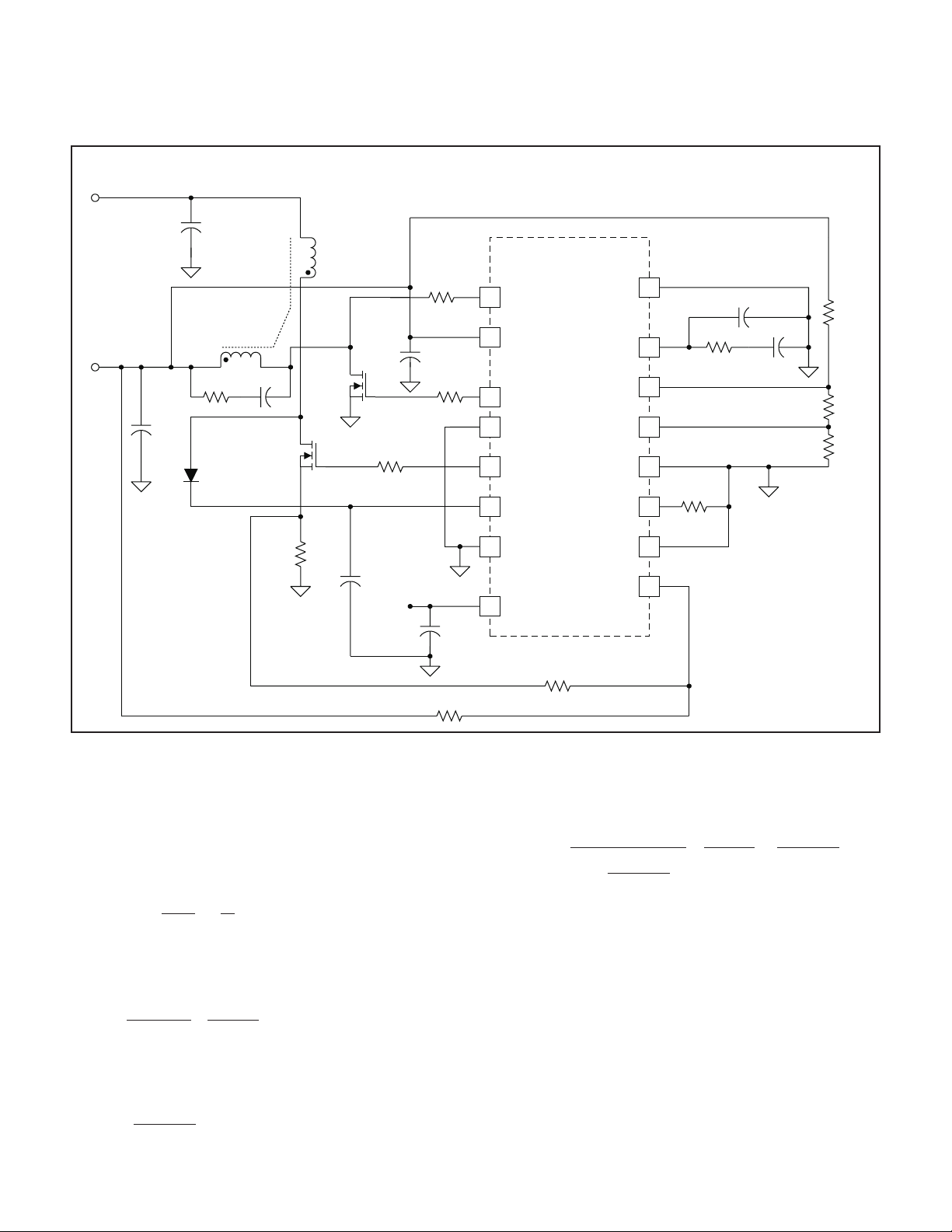
Start Up
-
The UCC39421 incorporates a unique feature to help it
start-up at low input voltages. If the input voltage is be
low 2.5V at start-up, a separate control circuit takes over
until V
OUT
or V
gets above 2.5V. In this mode, the
PUMP
charge MOSFET is turned on for 5µsec, or until the volt
age on the ISENSE pin reaches 36mV, whichever occurs
first. The charge MOSFET then remains off for a fixed
time of 2.5µsec, and the body diode of the synchronous
rectifier MOSFET is used to supply current to the output.
This cycle repeats until either V
-
2.5V. This results in constant off time control, with a mini
OUT
or V
PUMP
mum switching frequency of approximately 120kHz. Dur
ing this low voltage start-up mode, all other internal
circuitry is off, including the synchronous rectifier drive
and the slope compensation current source. The peak in
ductor current during this mode is limited to:
=
.036
R
SENSE
I
PEAK
15
-
-
exceeds
-
-
-
(13)

APPLICATION INFORMATION (cont.)
UCC29421/2
UCC39421/2
V
IN
R
SENSE
L
V
PUMP
C
PUMP
2.5V < V
PUMP
2.5V < V
NORMAL PWM
OUT
A
B
UCC39421
MUX
A/B
–
+
2.5V < V
LPM < V
5µsec
DELAY
Q
Q
2.5µsec
DELAY
PUMP
COMP
S
R
V
IN
DRIVER
+
–
36mV
V
+
PUMP
Figure 12. Simplified diagram of low voltage start-up and charge pump control logic.
C
FLY
D
BODY
V
OUT
C
OUT
UDG-98121
If input voltages below 2.5V are expected, it is important
to use a low voltage logic N-channel MOSFET (with a
threshold voltage around 1V or less) to guarantee
start-up at full load.
A block diagram of the low voltage start-up logic is
shown in Fig 12.
Anti Cross-Conduction and Adaptive Synchronous
Rectifier Commutation Logic
When operating in the continuous conduction mode
(CCM), the charge MOSFET and the synchronous recti
fier MOSFET are simply driven out of phase, so that
when one is on the other is off. There is a built-in time
delay of about 30nsec to prevent any cross-conduction.
In the event that the converter is operating in the discon
tinuous conduction mode (DCM), the synchronous recti
fier needs to be turned off sooner, when the rectifier
current drops to zero. Otherwise, the output will begin to
discharge as the current reverses and goes back through
the rectifier to the input. (This obviously cannot happen
when using a conventional diode rectifier). To prevent
this, the UCC39421 incorporates a high speed compara
tor which senses the voltage on the synchronous rectifier
(using the RSEN input) for purposes of commutation. In
the boost and SEPIC topologies, the synchronous rectifier is turned off when the voltage on the RSEN pin goes
negative with respect to V
tant to have the V
pin well decoupled.
OUT
. For this reason it is impor
OUT
In the flyback topology however (using a ground refer
enced N-channel MOSFET rectifier), the rectifier voltage
is sensed on the MOSFET drain, with respect to ground
rather than V
. The voltage polarity in this case is op
OUT
posite that of the boost and SEPIC topologies. This prob
lem is solved with the adaptive logic within the
UCC39421. During each charge cycle, while the
N-channel charge FET is on, a latch is set if the voltage
on the RSEN pin exceeds V
/2. This indicates a flyback
IN
topology, since this node will be equal to or greater than
-
-
at this time. In the case of the boost and the SEPIC,
V
IN
the voltage at the RSEN input will be near or below
ground, and the latch will not be set. This allows the
UCC39421 to sense which topology is in use and adapt
the synchronous rectifier commutation logic accordingly.
Note that the RSEN input must have a series resistor to
limit the current when going below ground. Values less
-
than or equal to 1k are recommended to prevent time de
lay due to stray capacitance.
-
-
-
-
-
16

APPLICATION INFORMATION (cont.)
Current Sense Amplifier and Leading Edge Blanking
UCC29421/2
UCC39421/2
This pin should be grounded if not used.
The UCC39421 includes a high speed current sense am
plifier with a nominal gain of 10 to minimize losses asso
ciated with the current sense resistor. The amplifier was
designed to provide good response and minimal propa
gation delay, allowing switching frequencies over 2MHz.
The current sense resistor should be chosen to provide a
maximum peak voltage of 100mV at full load, with the
minimum input voltage.
A leading edge blanking time of 40nsec is provided to fil
ter out leading edge spikes in the current sense wave
form. In most applications, this will eliminate the need for
a filter cap on the ISENSE pin.
Overcurrent Protection
The UCC39421 includes a peak current limit function. If
the voltage on the ISENSE pin exceeds 0.15V after the
initial blanking period, the pulse will be terminated and
the charge MOSFET will be turned off.
Sync/Shutdown Input
The SYNC/SD pin has two functions; it may be used to
synchronize the UCC39421’s switching frequency to an
external clock, or to shutdown the IC entirely. In shutdown, the quiescent current is reduced to just a few
microamps.
To synchronize the internal clock to an external source,
the SYNC/SD pin must be driven high, above 2.0V minimum. The circuitry syncs to the rising edge of the input,
the pulse width is not critical.
To shutdown the converter, the SYNC/SD pin must be
held high (above 2.0V) for a minimum of 20µsec.
-
Changing the Low Power Mode Threshold
For some applications the user may want to lower the
Low Power (LP) mode threshold, or even eliminate this
feature altogether. For example, if a boost topology is
being used, and the input voltage is below 2.5V, the gate
drive to the charge FET may want to be derived from the
pump (or output) voltage under all load conditions, rather
than from V
allowed to operate in LP mode.
-
Although the LP mode threshold is internally fixed at
. This means the converter would never be
IN
0.5V (referenced to the pin), the point at which the LP
mode is entered can be easily modified by adding a sin
gle resistor, as shown in Fig 13. Resistor R
divider with R
SLOPE
(used for slope compensation) and
BIAS
adds a DC offset to the current sense input, raising the
output voltage of the sense amplifier and “fooling” the LP
mode comparator into thinking the load is higher than it
is. The required bias resistor to transition out of LP mode
for a given peak current can be calculated using the following equation:
R
BIAS
RV
=
•
SLOPE OUT
IR
−•002.
PEAK SENSE
Due to the current sense amplifier gain of 10 and the internal offset of 300mV, an offset of just 20mV or more at
the ISENSE pin will inhibit LP mode altogether. Note that
inhibiting LP mode does not prevent PFM from working,
as long as the PFM pin is set to a voltage higher than:
10 0 3•+
VV
()
ISENSE
.
-
forms a
(14)
(15)
FB
COMP
UCC39421
500mV
17
1.25V
18
PWM
CONTROL
DRIVE
+
300mV
LP
MODE
LOGIC
X10
Figure 13. Modifying Low Power (LP) mode threshold.
17
6
12
CHRG
ISENSE
R
R
SLOPE
BIAS
R
SENSE
C
OUT
C
OUT
UDG-98213

Y
APPLICATION INFORMATION (cont.)
UCC29421/2
UCC39421/2
VOUT
R1
R2
RT2
RT1
9ISENSE
2N7002
1
2
3
4
5
6
7
8
RSEN
VOUT
VGRECT
PGND
CHRG
VPUMP
CP
VIN
UCC39401
SYNC/SD
RSEL
COMP
FB
PFM
GND
RT
16
15
14
13
12
11
10
Figure 14. Changing the PWM frequency.
+3.0–8.0V
C
IN
100µF
16V
+
L1
6.8µH
FREQUENC
CONTROL
95%
Vin=3.3V Vin=5V
90%
85%
80%
75%
70%
EFFICIENCY
65%
60%
0.001 0.01 0.1 1
OUTPUT CURRENT (Amps)
Figure 15. Non-synchronous 12V boost efficiency.
(f=550KHz, L=6.8
µ
H DT3316P-682, IRF7601,
MBR0530, VPFM=0.5V)
UCC39421
1
RSEN
+12V
C
OUT
100µF
16V
+
D1
MBR0530T
R
SENSE
0.05Ω
Q1
(N)
+V
RG1
4.7
IN
2
VOUT
3
N/C
VGRECT
4
PGND
5
VGCHRG
6
VPUMP
7 10
CP
VIN
0.1µF
R
Figure 16. Non-synchronous boost converter for higher output voltages.
18
RSEL
COMP
FB
PFM
GND
RT
SYNC/SD
ISENSE
SLOPE
1.5K
16
15
14
13
12
11
R3
249K
C
POLE
1%
1.25V
R
COMP
C
COMP
R2
17.8K
1%
R1
11K
1%
RT
100K
98
UDG-98206

APPLICATION INFORMATION (cont.)
Programming the PWM Frequency
Some applications may want to remain in a fixed fre
quency mode of operation, even at light load, rather than
going into PFM mode. This lowers efficiency at light load.
One way to improve the efficiency while maintaining fixed
frequency operation is to lower the PWM frequency un
der light load conditions. This can be easily done, as
shown in Fig 14. By adding a second timing resistor and
a small MOSFET switch, the host can switch between
two discrete frequencies at any time.
Non-Synchronous Boost for Higher Output Voltage
Applications
The UCC39421 can also be used in a non-synchronous
application to provide output voltages greater than 8
volts from low voltage inputs. An example of a 12V boost
application is shown in Fig 16. Since none of the IC pins
are exposed to the boosted voltage, the output voltage is
limited only by the ratings of the external MOSFET, recti
fier and filter capacitor. At these higher output voltages,
good efficiency is maintained since the rectifier drop is
small compared to the output voltage. Note that PFM
mode can still be used to maintain high efficiency at light
load. Typical efficiency causes are shown in Fig. 15.
Since all the power supply pins (VIN, VOUT, VPUMP)
operate off the input voltage, it must be >2.5V and high
enough to assure proper gate drive to the charge FET.
UCC39422 Features
The UCC39422 is a 20 pin device which adds a reset
function and an uncommitted comparator to the
UCC39421. A simplified diagram of the reset circuit is
shown in Fig 17.
UCC29421/2
UCC39421/2
The reset circuit monitors the voltage at the feedback
(FB) pin and issues a reset if the feedback voltage drops
below 1.175V. This represents a 6% drop in output volt
age. Monitoring the voltage internally at the FB pin elimi
nates the need for another external voltage divider. The
RESET output is an open drain output which is active
low during reset. It stays low until the feedback voltage is
above 1.175V for a period of time called the reset pulse
width, which is user programmable. An external capacitor
on the RSADJ pin and an internal 1µA current source de
termine the reset pulse width, according to the following
equation:
tC
where t
C
RESET
An adaptive glitch filter is included to prevent nuisance
trips. This is implemented using a gm amplifier to charge
an 8pF capacitor to 1.175V before declaring a reset. This
provides a delay which is inversely proportional to the
magnitude of the feedback voltage error. The delay time
is approximated by the following equation:
t
where t
Note that the maximum current from the gm amplifier is
limited to 2µA, limiting the minimum time delay to
4.8µsec.
≅•118.
RESET RESET
RESET
is the reset pulse width in seconds, and
is the capacitor value in microFarads (µF).
025
DELAY
DELAY
≅
1 175..
−
is the filter delay time in microseconds.
secµ
V
FB
-
-
-
(16)
(17)
17
FB
1.175V
Figure 17. Reset circuitry.
gm=1/26k
8pF
1.175V
SQ
QR
19
1.175V
1µA
20
1 RESET
RSADJ
C
RESET
UDG-98121

APPLICATION INFORMATION (cont.)
A typical application schematic using the UCC39422 is
shown in Fig. 18. In this example, R1 and R2 have been
slected to trip the LOWBAT output when V
2.0V. Note that the RESET
and LOWBAT outputs are
open drain and require a pullup.
Selecting the Inductor
The inductor must be chosen based on the desired oper
ating frequency and the maximum load current. Higher
frequencies allow the use of lower inductor values, re
ducing component size. Higher load currents will require
larger inductors with higher current ratings and less wind
ing resistance to minimize losses. The inductor must be
rated for operation at the highest anticipated peak cur
rent. Refer to equations (8) and (12) to calculate the
peak inductor current for a boost or flyback design,
based on V
IN,VOUT
, maximum load, frequency and in
ductor value. Some manufacturers rate their parts for
drops below
IN
UCC29421/2
UCC39421/2
maximum energy storage in micro-Joules (µJ). This is
expressed by:
ELI
=••052.
where E is the required energy rating in micro-Joules. L
is the inductor value in microHenries (µH) (with current
applied), and I
inductor will see in the application. Another way in which
inductor ratings are sometimes specified is the maximum
volt-seconds applied. This is given simply by:
-
ET
•=
where ET is the required rating in V-µsec, D is the duty
cycle for a given V
-
quency in MHz. Refer to equations (7) and (11) to calcu
late the duty cycle for a CCM boost or flyback converter.
PEAK
is the peak current in amps that the
PEAK
VD
•
IN
f
and V
IN
, and f is the switching fre
OUT
(18)
(19)
-
-
+V
V
OUT
IN
RESET* (ACTIVE LOW)
RG
0.1µF
RG
0.1µF
0.1µF
10 VIN
1
2
3
4
5
6
7
8
9
UCC39422
RSEN
RSEN
VOUT
VGRECT
PGND
CHRG
VPUMP
CP
RSEL
COMP
FB
PFM
GND
RT
SYNC/SD
ISENSE
19
18
17
16
15
14
13
12
11VDET
C
RESET
20VIN
C
POLE
R1
C
COMP
150k
47pF
R2
+V
IN
R
COMP
RT
100k
250k
+C
+C
OUT
IN
Q1 (P)
Q1 (N)
+V
IN
R
SENSE
L1
1k
Figure 18. Typical UCC39422 application.
LOWBAT (ACTIVE HIGH)
20
R
SLOPE
THRESHOLD = 2.0V
UDG-99034

APPLICATION INFORMATION (cont.)
Table III. SMT commercial inductor manufacturers.
Coilcraft Inc. • (800) 322-2645.
1102 Silver Lake RD, Cary, IL 60013
Coiltronics Inc. • (407) 241-7876
6000 Park of Commerce Blvd, Boca Raton, FL 33487
Dale Electronics, Inc. • (605) 665-9301
East Highway 50, Yankton, SD 57078
Pulse Engineering Ltd. • (204) 633-4321
300 Keewatin Street, Winnipeg, MB R2X 2R9
Sumida • Voice (65) 296-3388 • Fax (65) 293-3390
Block 996, Bendemeer Rd., #04-05/06 Singapore 33944
BH Electronics • (612) 894-9590
12219 Wood Lake Drive, Burnsville, MN 55337
Tokin America Inc. • (408) 432-8020
155 Nicholson Lane, San Jose CA 95134
In any case, the inductor must use a low loss core de
signed for high frequency operation. High frequency fer
rite cores are recommended. Some manufacturers of
off-the-shelf surface mount designs are listed in Table III.
For flyback and SEPIC topologies, use a two winding
coupled inductor. SEPIC designs can also use two discrete inductors.
Selecting the Filter Capacitor
The input and output filter capacitors must have low ESR
and low ESL. Surface mount tantalum, OSCON or
multi-layer ceramics (MLC’s) are recommended. The capacitor selected must have the proper ripple current rating for the application. Some recommended capacitor
types are listed in Table IV.
Table IV. Recommended SMT Filter Capacitors
Manufacturer Part Number Features
AVX TPS series Low ESR tantalum
Kemet T410 series Low ESR tantalum
Murata GRM series Low ESR ceramic
Sanyo OSCON series Low ESR organic
Sprague 591D series Low ESR, low profile
tantalum
594D series Low ESR tantalum
Tokin Y5U, Y5V Type Low ESR ceramic
Circuit Layout and Grounding
As with any high frequency switching power supply, cir
cuit layout, hookup and grounding are critical for proper
operation. Although this may be a relatively low power,
low voltage design, these issues are still very important.
The MOSFET turn-on and turn-off times necessary to
maintain high efficiency at high switching frequencies of
1MHz or more result in high dv/dt and di/dt’s. This makes
stray circuit inductance especially critical. In addition, the
high impedances associated with low power designs,
UCC29421/2
UCC39421/2
such as in the feedback divider, make them especially
susceptible to noise pickup.
Layout
The component layout should be as tight as possible to
minimize stray inductance. This is especially true of the
high current paths, such as in series with the MOSFETs
and the input and output filter caps.
The components associated with the feedback, compen
sation and timing should be kept away from the power
components (MOSFETs, inductor). Keep all components
as close to the IC pins as possible. Nodes that are espe
cially noise sensitive are the FB and RT pins. Other sen
sitive pins are COMP and PFM.
Grounding
-
A ground plane is highly recommended. The PGND pin
-
of the UCC39421 should be close to the grounded end of
the current sense resistor, the input filter cap, and the
output filter cap. The GND pin should be close to the
grounded end of the RT resistor, the feedback divider resistor, the ISENSE cap (if used), and the compensation
network.
MOSFET Gate Resistors
The UCC39421 includes low impedance CMOS output
drivers for the two external MOSFET switches. The
CHRG output has a nominal resistance of 4
RECT has a nominal resistance of 2
quency operation using low gate charge MOSFETs, no
gate resistors are required. To reduce high frequency
ringing at the MOSFET gates, low value series gate re
sistors may be added. These should be non-inductive re
sistors, with a value of 2
to 10 , depending on the
frequency of operation. Lower values will result in better
switching times, improving efficiency.
Minimizing Output Ripple and Noise Spikes
The amount of output ripple will be determined primarily
by the type of output filter capacitor and how it is con
nected in the circuit. In most cases, the ripple will be
dominated by the ESR (Equivalent Series Resistance)
and ESL (Equivalent Series Inductance) of the cap,
rather than the actual capacitance value. Low ESR and
ESL capacitors are mandatory in achieving low output
ripple. Surface mount packages will greatly reduce the
ESL of the capacitor, minimizing noise spikes. To further
minimize high frequency spikes, a surface mount ce
ramic capacitor should be placed in parallel with the main
filter cap. For best results, a capacitor should be chosen
whose self-resonant frequency is near the frequency of
the noise spike. For high switch frequencies, ceramic ca
pacitors alone may be used, reducing size and cost.
For high fre-
-
-
-
, and the
-
-
-
-
-
21

APPLICATION INFORMATION (cont.)
For applications where the output ripple must be ex
tremely low, a small LC filter may be added to the output.
The resonant frequency should be below the selected
switching frequency, but above that of any dynamic
loads. The filter’s resonant frequency is given by:
f
RES
1
=
LC
•
2π
Where f is the frequency in Hz, L is the filter inductor
value in Henries and C is the filter capacitor value in
Farads. It is important to select an inductor rated for the
maximum load current and with minimal resistance to re
(20)
UCC29421/2
UCC39421/2
duce losses. The capacitor should be a low impedance
type, such as a tantalum.
If an LC ripple filter is used, the feedback point can be
taken before or after the filter, as long as the filter’s reso
nant frequency is well above the loop crossover fre
quency. Otherwise the additional phase lag will make the
loop unstable. The only advantage to connecting the
feedback after the filter is that any small voltage drop
across the filter inductor will be corrected for in the loop,
providing the best possible voltage regulation. However,
the resistance of the inductor is usually low enough that
-
the voltage drop will be negligible.
-
-
UNITRODE CORPORATION
7 CONTINENTAL BLVD. • MERRIMACK, NH 03054
TEL. (603) 424-2410 • FAX (603) 424-3460
22
 Loading...