Page 1
UCC28083, UCC28084, UCC28085, UCC28086
UCC38083, UCC38084, UCC38085, UCC38086
SLUS488D -- SEPTEMBER 2002 -- REVISED AUGUST 2006
8-PIN CURRENT MODE PUSH-PULL PWM CONTROLLERS
WITH PROGRAMMABLE SLOPE COMPENSATION
FEATURES
D Programmable Slope Compensation
D Internal Soft -Start on the UCC38083/4
D Cycle-by-Cycle Current Limiting
D Low Start-Up Current of 120 μAand1.5mA
Typical Run C urrent
D Single External Component Oscillator
Programmablefrom50kHzto1MHz
D High-Current Totem-Pole Dual Output Stage
Drives Push-Pull Configuration with 1-A Sink
and 0.5-A Source Capability
D Current Sense Discharge Transistor to
Improve Dynamic Response
D Internally Trimmed Bandgap Reference
D Undervoltage Lockout with Hysteresis
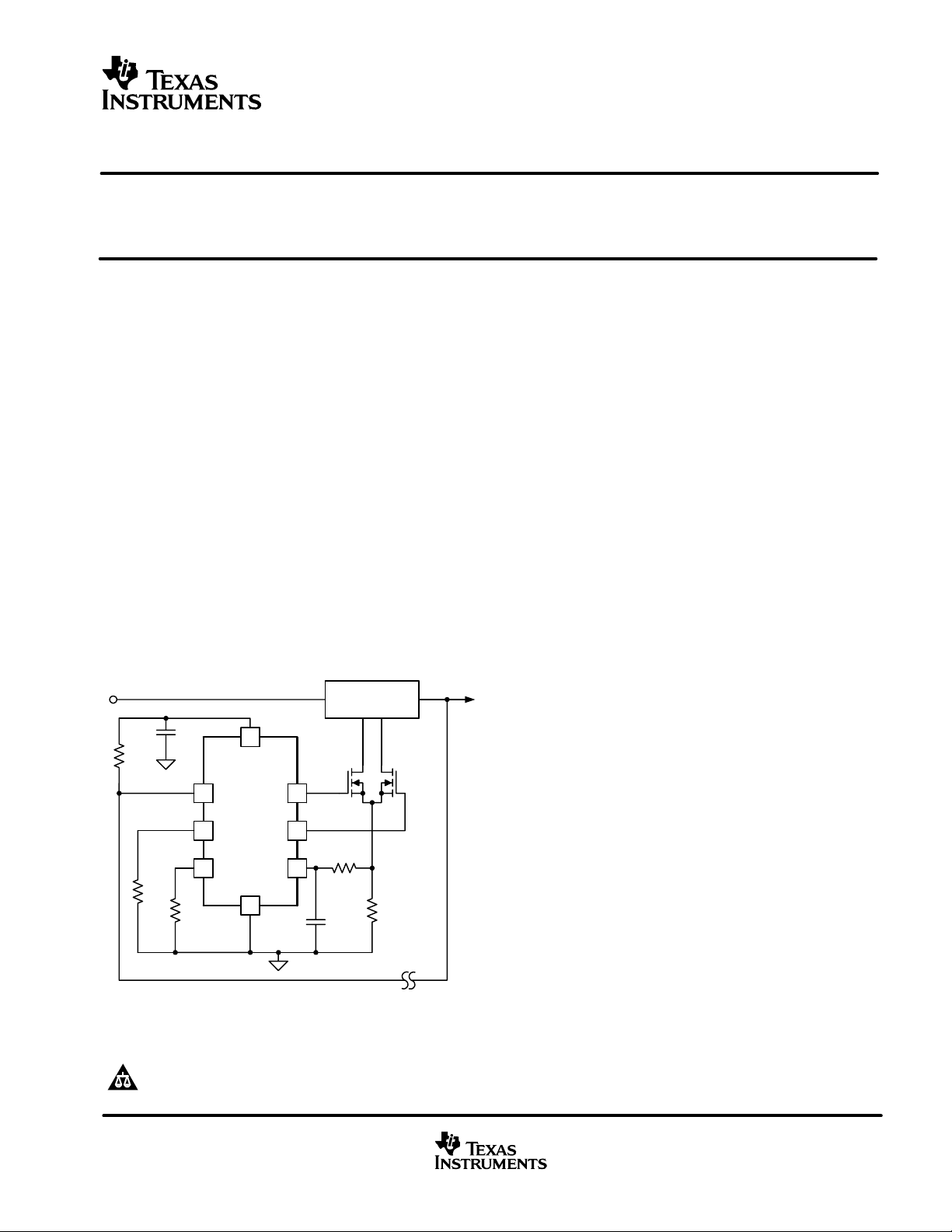
BASIC APPLICATION
V
IN
VDD
UCC3808x
OUTA
CTRL
OUTB
RT
ISET
R
T
R
SET
CS
GND
POWER
TRANSFORMER
R
F
C
F
R
S
FEEDBACK
APPLICATIONS
D High-Efficiency Switch-Mode Power Supplies
D Telecom dc-to-dc C onverters
D Point-of-Load or Point-of-Use Power Modules
D Low-Cost Push-Pull and Half-Bridge
Applications
DESCRIPTION
The UCC38083/4/5/6is a family of BiCMOS pulse width
modulation (PWM) controllers for dc-to-dc or off-line
fixed-frequency current-mode switching power
supplies. The dual output stages are configured for the
push-pull topology. Both outputs switch at half the
oscillator frequency using a toggle flip-flop. The dead
time between the two outputs is typically 110 ns, limiting
each output’s duty cycle to less than 50%.
The new UCC3808x family is based on the UCC3808A
architecture. The major differences include the addition
of a programmable slope compensation ramp to the CS
signal and the removal of the error amplifier.The current
flowing out of the ISET pin through an external resistor
is monitored internally to set the magnitude of the slope
compensation function. This device also includes an
V
OUT
internal discharge transistor from the CS pin to ground,
which is activated at each clock cycle after the pulse is
terminated. This discharges any filter capacitance on
the CS pin during each cycle and helps minimize filter
capacitor values and current sense delay.
The UCC38083 and the UCC38084 devices have a
typical soft-start interval time of 3.5 ms while the
UCC38085 and the UCC38086 has less than 100 μsfor
applications where internal soft-start is not desired.
The UCC38083 and the UCC38085 devices have the
turn-on/off thresholds of 12.5 V / 8.3 V, while the
UCC38084 and the UCC38086 has the turn-on/off
thresholds of 4.3 V / 4.1 V.Each device is offered in 8-pin
TSSOP (PW), 8-pin SOIC (D) and 8-pin PDIP (P)
packages.
Please be aware that an important notice concerning availability, standard warranty, and use in critical applications ofTexas Instruments
semiconductor products and disclaimers thereto appears at the end of this data sheet.
PRODUCTION DATA information is current as of publication date.
Products conform to specifications per the terms of Texas Instruments
standard warranty. Production processing does not necessarily include
testing of all parameters.
UDG--01080
www.ti.com
Copyright © 2002-- 2006, Texas Instruments Incorporated
1
Page 2

UCC28083, UCC28084, UCC28085, UCC28086
INTERNA
L
UCC38083, UCC38084, UCC38085, UCC38086
SLUS488D -- SEPTEMBER 2002 -- REVISED AUGUST 2006
ORDERING INFORMATION
THERMAL RESISTANCE TABLE
PACKAGE
SOIC--8 (D) 42 84 to 160
PDIP--8 (P) 50 110
TSSOP--8 (PW) 32
NOTES: (1) Specified θja (junction to ambient) is for devices mounted to 5-inch2FR4 PC board
T
A
°
-- 4 0 °Cto85°C
°
0°Cto70°C
†
The D and PW packages are available taped and reeled. Add R suffix to device type, e.g. UCC28083DR (2500 devices
per reel) or UCC38083PWR (2000 devices per reel).
D OR P PACKAGE
with one ounce copper where noted. When resistance range is given, lower values
are for 5 inch
used 0.635-mm trace widths for power packages and 1.3-mm trace widths for
non-power packages with a 100-mil x 100-mil probe land area at the end of each
trace.
(2). Modeled data. If value range given for θja, lower value is for 3x3 inch. 1 oz internal
copper ground plane, higher value is for 1x1-inch. ground plane. All model data
assumes only one trace for each non-fused lead.
INTERNAL
SOFT START
°
°
(TOP VIEW)
3.5 ms
75 μs
3.5 ms
75 μs
2
aluminum PC board. Test PWB was 0.062 inch thick and typically
UVLO PACKAGES
ON OFF SOIC-8 (D) PDIP-8 (P) TSSOP-8 (PW)
12.5 V 8.3 V UCC28083D UCC28083P UCC28083PW
4.3 V 4.1 V UCC28084D UCC28084P UCC28084PW
12.5 V 8.3 V UCC28085D UCC28085P UCC28085PW
4.3 V 4.1 V UCC28086D UCC28086P UCC28086PW
12.5 V 8.3 V UCC38083D UCC38083P UCC38083PW
4.3 V 4.1 V UCC38084D UCC38084P UCC38084PW
12.5 V 8.3 V UCC38085D UCC38085P UCC38085PW
4.3 V 4.1 V UCC38086D UCC38086P UCC38086PW
θjc(°C/W) θja(°C/W)
AVAILABLE OPTIONS
(1)
(1)
(2)
PW PACKAGE
232 to 257
(TOP VIEW)
(2)
CTRL
ISET
2
CS
RT
1
2
3
4
8
7
6
5
VDD
OUTA
OUTB
GND
OUTA
VDD
CTRL
ISET
www.ti.com
1
2
3
4
8
7
6
5
OUTB
GND
RT
CS
Page 3

UCC28083, UCC28084, UCC28085, UCC28086
Minimumoperatingvoltage
V
UCC38083, UCC38084, UCC38085, UCC38086
SLUS488D -- SEPTEMBER 2002 -- REVISED AUGUST 2006
DD
†
20 mA.........................................................................
+0.3 V..................................................
absolute maximum ratings over operating free-air temperature (unless otherwise noted)
Supply voltage, VDD(IDD<10mA) 15V.............................................................
Supply current, I
Sink current (peak): OUTA 1.0 A................................................................
Source current (peak): OUTA -- 0 . 5 A...............................................................
Analog inputs: CTRL --0.3 V to V
Power dissipation at T
Power dissipation at T
Power dissipation at T
Junction operating temperature, T
Storage temperature, T
Lead temperature (soldering 10 seconds) 300°C......................................................
†
Stresses beyond those listed under “absolute maximum ratings” may cause permanent damage to the device. These are stress ratings only,and
functional operation of the device at these or any other conditions beyond those indicated under “recommended operating conditions” is not
implied. Exposure to absolute -maximum-rated conditions for extended periods may affect device reliability. All voltages are with respect to GND.
Currents are positive into, and negative out of the specified terminal.
DD
OUTB 1.0 A................................................................
OUTB -- 0 . 5 A...............................................................
CS --0.3 V to V
R
(minimum) >5 kΩ......................................................
SET
R
(--100 μA<IRT< 100 μA) --0.3 V to 2.0 V.....................................
T
=25°C (P package) 1 W....................................................
A
=25°C (D package) 650 mW................................................
A
=25°C (PW package) 400 mW..............................................
A
J
stg
DD
+0.3 V, not to exceed 6 V.....................................
-- 5 5 °C to 150°C...................................................
-- 6 5 °C to 150°C............................................................
electrical characteristics over recommended operating virtual junction temperature range,
V
= 10 V (See Note 1),1-μF capacitor from VDD to GND, RT= 165 kΩ,RF=1kΩ,CF= 220 pF,
DD
R
=50kΩ,TA=--40°Cto85°C for UCC2808x, TA=0°Cto70°C for UCC3808x, TA=T
SET
J
(unless otherwise noted)
overall
PARAMETER TEST CONDITIONS MIN TYP MAX UNITS
Start-up current VDD < UVLO start threshold voltage 120 200 μA
Supply current CTRL = 0 V, CS = 0 V,
SeeNote1
1.5 2.5 mA
undervoltage lockout
PARAMETER TEST CONDITIONS MIN TYP MAX UNITS
Start threshold voltage
Minimum operatingvoltage
after start
Hysteresis voltage
UCC38083/5 SeeNote1 11. 5 12.5 13.5
UCC38084/6 4.1 4.3 4.5
UCC38083/5 7.6 8.3 9.0
UCC38084/6 3.9 4.1 4.3
UCC38083/5 3.5 4.2 5.1
UCC38084/6 0.1 0.2 0.3
oscillator
PARAMETER TEST CONDITIONS MIN TYP MAX UNITS
Frequency 2xf(OUTA) 180 200 220 kHz
Voltage amplitude SeeNote2 1.4 1.5 1.6 V
Oscillator fall time (dead time) 110 220 ns
RT pin voltage 1.2 1.5 1.6 V
www.ti.com
3
Page 4

UCC28083, UCC28084, UCC28085, UCC28086
f
f
V
UCC38083, UCC38084, UCC38085, UCC38086
SLUS488D -- SEPTEMBER 2002 -- REVISED AUGUST 2006
electrical characteristics over recommended operating virtual junction temperature range,
V
= 10 V (See Note 1),1-μF capacitor from VDD to GND, RT= 165 kΩ,RF=1kΩ,CF= 220 pF,
DD
R
=50kΩ,TA=--40°Cto85°C for UCC2808x, TA=0°Cto70°C for UCC3808x, TA=T
SET
(unless otherwise noted)
current sense
PARAMETER TEST CONDITIONS MIN TYP MAX UNITS
Gain SeeNote3 1.9 2.2 2.5 V/V
Maximum input signal voltage CTRL = 5 V, See Note 4 0.47 0.52 0.57 V
CS to output delay time CTRL = 3.5 V, 0 mV ≤ CS ≤ 600 mV 100 200 ns
Source current --200 nA
Sink current
Overcurrent threshold voltage 0.70 0.75 0.80 V
CTRL to CS o
set voltage
CS=0.5V, RT=2.0V,
SeeNote5
CS = 0 V, 25°C 0.55 0.70 0.90 V
CS = 0 V 0.37 0.70 1.10 V
3 7 12 mA
pulse width modulation
PARAMETER TEST CONDITIONS MIN TYP MAX UNITS
Maximum duty cycle Measured at OUTA or OUTB, See Note 7 48% 49% 50%
Minimum duty cycle CTRL = 0 V 0%
J
output
PARAMETER TEST CONDITIONS MIN TYP MAX UNITS
Low-level output voltage (OUTA or OUTB) I
High-level output voltage (OUTA or OUTB) I
Rise time C
Fall time C
= 100 mA 0.5 1.0
OUT
= --50 mA, (VDD -- VOUT), See Note 6 0.5 1.0
OUT
=1nF 25 60
LOAD
=1nF 25 60
LOAD
ns
soft-start
PARAMETER TEST CONDITIONS MIN TYP MAX UNITS
OUTA/OUTB soft-start interval time,
UCC38083/4
OUTA/OUTB soft-start interval time,
UCC38085/6
CTRL = 1.8 V, CS = 0 V,
Duty cycle from 0 to full, See Note 8
CTRL = 1.8 V, CS = 0 V,
Duty cycle from 0 to full, See Note 8
1.3 3.5 8.5 ms
30 75 110 μs
slope compensation
PARAMETER TEST CONDITIONS MIN TYP MAX UNITS
I
, peak I
RAMP
NOTE 1: For UCCx8083/5, set VDD above the start threshold before setting to 10 V.
NOTE 2: Measured at ISET pin.
ΔV
CTRL
NOTE 3: Gain is defined by A =
NOTE 4: Measured at trip point of latch with CS ramped from 0.4 V to 0.6 V.
NOTE 5: This internal current sink on the CS pin is designed to discharge and external filter capacitor. It is not intended to be a dc sink path.
NOTE 6: Not 100% production tested. Ensured by design and also by the rise time test.
NOTE 7: For devices in PW package, parameter tested at wafer probe.
NOTE 8: Ensured by design.
,0≤ VCS≤ 0.4 V.
ΔV
CS
, peak = 30 μA, Full duty cycle 125 150 175 μA
SET
4
www.ti.com
Page 5
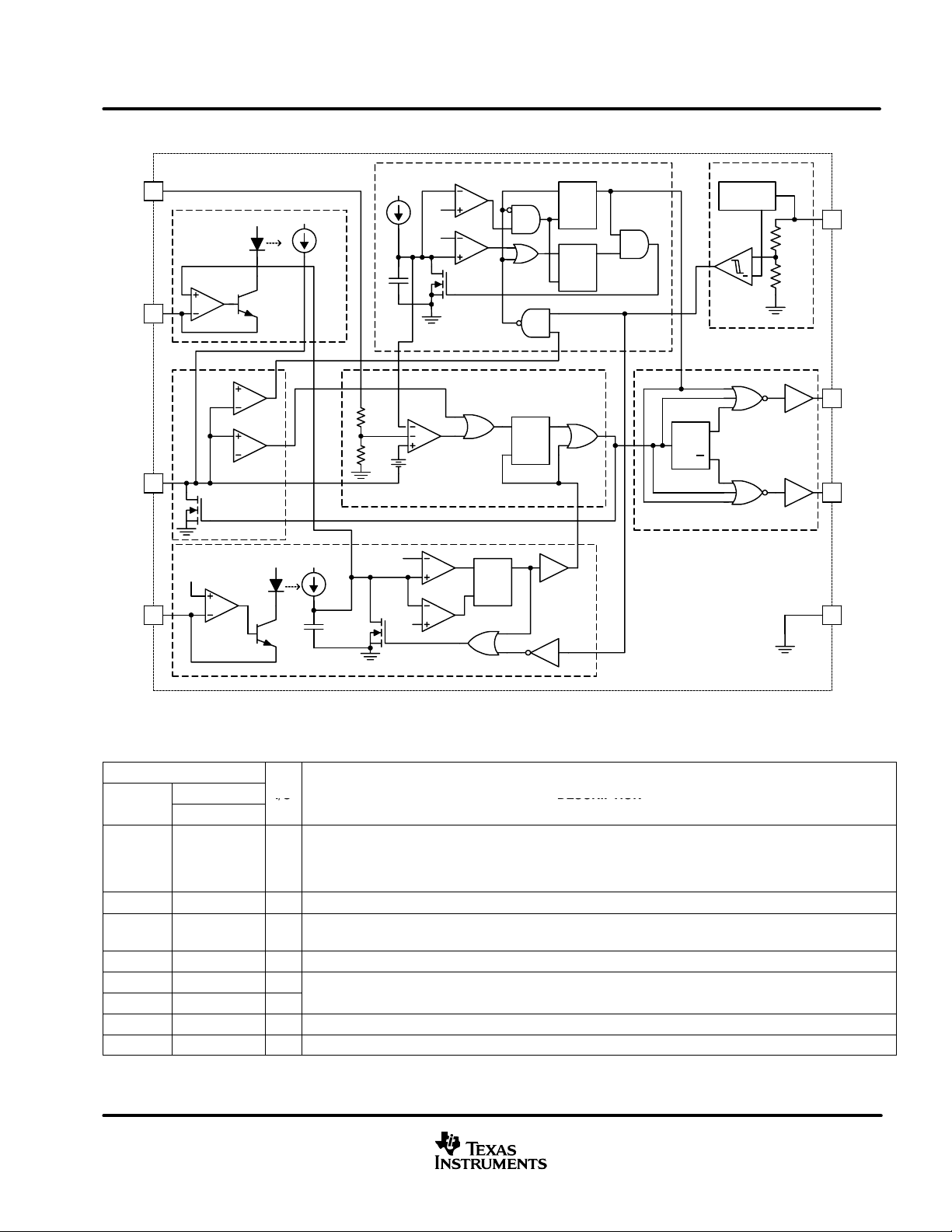
functional block diagram
I/ODESCRIPTIO
N
A
UCC28083, UCC28084, UCC28085, UCC28086
UCC38083, UCC38084, UCC38085, UCC38086
SLUS488D -- SEPTEMBER 2002 -- REVISED AUGUST 2006
ISET
CS
RT
Soft Start and Fault Latch
1CTRL
Slope Circuit
C
T
I
2
CS Circuitry
0.75V
3
1.5V
4
SLOPE
0.5V
5xI
=
SET
I
SLOPE
I
C
CT
Iss
0.5V
Vdd--1
Css
PWM Comparator/Latch Output Driver
80 k
Ω
Ω
60 k
0.3 V
Oscillator
1.5V
T
0.2V
SQ
R
SQ
R
SQ
R
SQ
R
T
Bias/UVLO
VREF
8
VDD
+
7
OUTA
Q
Q
6
OUTB
5
GND
UDG--01081
Terminal Functions
TERMINAL
NAME
CS 3 I The current-sense input to the PWM comparator, the cycle-by-cycle peak current comparator, and the
CTRL 1 I Error voltage input to PWM comparator.
GND 5 -- Reference ground and power ground for all functions. Due to high currents, and high-frequency operation
ISET 2 I Current selection for slope compensation.
OUTA 7 O
OUTB 6 O
RT 4 I Programs the oscillator.
VDD 8 I Power input connection.
PACKAGE
DORP
I/O DESCRIPTION
overcurrent comparator. The overcurrent comparator is only intended for fault sensing. Exceeding the
overcurrent threshold causes a soft-start cycle. An internal MOSFET discharges the current-sense filter
capacitor to improve dynamic performance of the power converter.
of the IC, a low-impedance circuit board ground plane is highly recommended.
lternating high-current output stages.
www.ti.com
5
Page 6
UCC28083, UCC28084, UCC28085, UCC28086
UCC38083, UCC38084, UCC38085, UCC38086
SLUS488D -- SEPTEMBER 2002 -- REVISED AUGUST 2006
detailed pin descriptions
CTRL: The error voltage is typically generated by a secondary-side error amplifier and transmitted to the
primary-side referenced UCC3808x by means of an opto-coupler. CTRL has an internal divider ratio of 0.45 to
maintain a usable range with the minimum V
full-cycle soft start while the UCC38085/6 does not.
For the UCC38083/4, soft-start is implemented as a clamp at the input to the PWM comparator. This causes
the output pulses to start near 0% duty cycle and increase until the clamp exceeds the CTRL voltage.
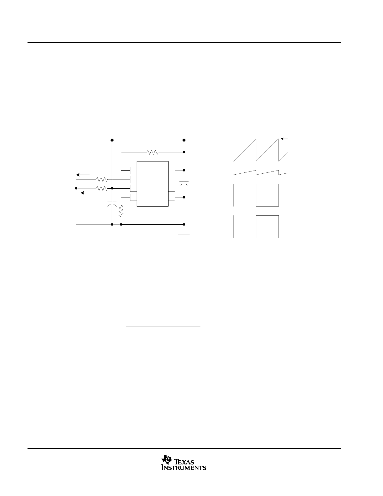
ISET: Program the slope compensation current ramp by connecting a resistor, RSET, from ISET to ground. The
voltage of the ISET pin tracks the 1.5-V internal oscillator ramp, as shown in Figure 1.
V(CS) VDD
10k
I
SET
I
RAMP
RSET
RF
1k
220pF
1
2
3
4
RT
165k
UCC38083
CTRL VDD
ISET
OUTA
CS
OUTB
RT
of 4.1 V. The UCC38083/UCC38084 family features a built-in
DD
I
RAMP, peak
IRAMP
GND
8
7
6
5
1uF
ISET
OUTA
OUTB
=5xI
SET, peak
Figure 1. Full Duty Cycle Output
The compensating current source, I
, at the CS pin is proportional to the ISET current, according to the
SLOPE
relation:
I
SLOPE
The ramping current due to I
= 5 × I
SET
develops a voltage across the effective filter impedance that is normally
SLOPE
(1)
connected from the current sense resistor to the CS input. In order to program a desired compensating slope
with a specific peak compensating ramp voltage at the CS pin, use the RSET value in the following equation:
RSET = V
Where V
OSC(peak)
OSC(peak)
×
RAMP VOLTAGE HEIGHT
= 1.5 V
5 × RF
(2)
Notice that the PWM Latch drives an internal MOSFET that will discharge an external filtering capacitor on the
CS pin. Thus, I
will appear to terminate when the PWM comparator or the cycle-by-cycle current limit
SLOPE
comparator sets the PWM latch. The actual compensating slope is not affected by premature termination of the
switching cycle.
6
www.ti.com
Page 7
UCC28083, UCC28084, UCC28085, UCC28086
UCC38083, UCC38084, UCC38085, UCC38086
SLUS488D -- SEPTEMBER 2002 -- REVISED AUGUST 2006
detailed pin descriptions (continued)
OUTA and OUTB: Alternating high-current output stages. Both stages are capable of driving the gate of a power
MOSFET. Each stage is capable of 500-mA peak-source current, and 1-A peak-sink current.
The output stages switch at half the oscillator frequency, in a push-pull configuration. When the voltage on the
internal oscillator capacitor is rising, one of the two outputs is high, but during fall time, both outputs are off. This
dead time between the two outputs, along with a slower output rise time than fall time, ensures that the two
outputs cannot be on at the same time. This dead time is typically 110 ns.
The high-current output drivers consist of MOSFET output devices, which switch from VDD to GND. Each output
stage also provides a very low impedance to overshoot and undershoot. This means that in many cases,
external Schottky clamp diodes are not required.
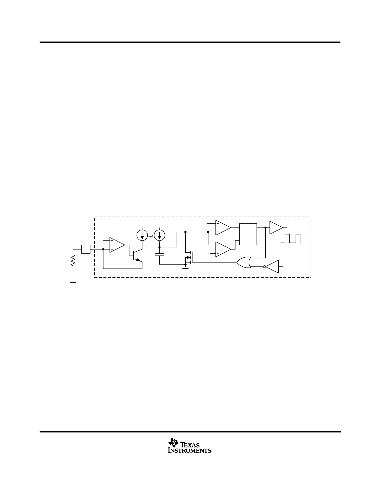
RT: The oscillator programming pin. The oscillator features an internal timing capacitor. An external resistor,
R
, sets a current from the RT pin to ground. Due to variations in the internal CT, nominal VRTof 1.5 V can vary
T
from 1.2 V to 1.6 V
Selecting RT as shown programs the oscillator frequency:
-- 1 2
1
f
OSC
− 2.0 × 10
-- 7
(3)
where f
RT =
OSC
1
28.7 × 10
is in Hz, resistance in Ω. The recommended range of timing resistors is between 25 kΩ and 698 kΩ.
For best performance, keep the timing resistor lead from the RT pin to GND (pin 5) as short as possible.
1.5 V
1.5 V
4
R
T
I
RT
Approximate Frequency =
I
CT
C
T
0.2 V
28.7 × 10
1
-- 1 2
× RT+2.0 × 10
SQ
R
-- 7
OSCILLATOR
OUTPUT
UDG--01083
Figure 2. Block Diagram for Oscillator
VDD: The power input connection for this device. Although quiescent VDD current is very low, total supply
current may be higher, depending on OUTA and OUTB current, and the programmed oscillator frequency. Total
VDD current is the sum of quiescent VDD current and the average OUT current. Knowing the operating
frequency and the MOSFET gate charge (Q
I
OUT
= QG× f
OSC
), average OUT current can be calculated from:
G
(4)
where f is the oscillator frequency.
To prevent noise problems, bypass VDD to GND with a ceramic capacitor as close to the chip as possible along
with an electrolytic capacitor. A 1-μF decoupling capacitor is recommended.
www.ti.com
7
Page 8
UCC28083, UCC28084, UCC28085, UCC28086
UCC38083, UCC38084, UCC38085, UCC38086
SLUS488D -- SEPTEMBER 2002 -- REVISED AUGUST 2006
APPLICATION INFORMATION
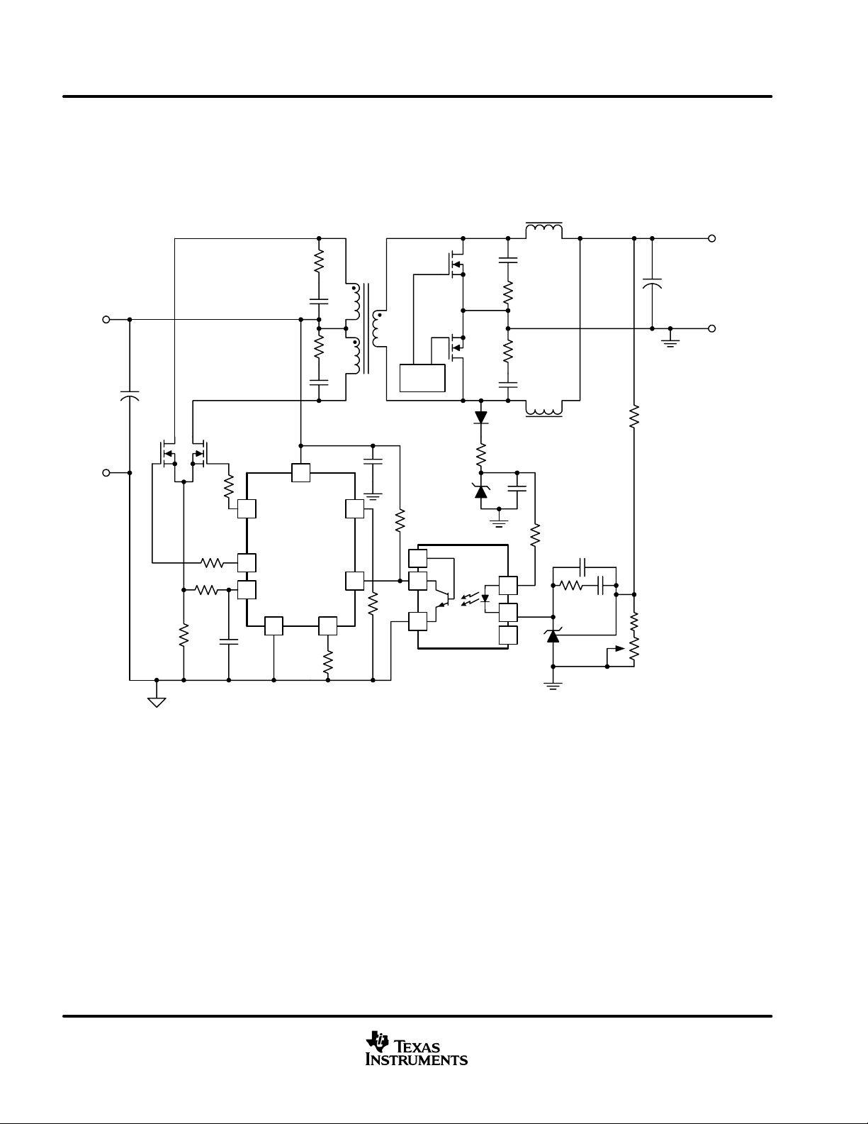
The following application circuit shows an isolated 12-VINto 2.5 V
push-pull converter with scalable output
OUT
power (20 W to 200 W). Note that the pinout shown is for SOIC-8 and PDIP-8 packages.
typical application
VIN=12V
+/--20%V
SR
DRIVE
F
1
ISET
2
μ
4RT
6
1CTRL
R
SET
165
k
Ω
5
4
1
2
3
TL431
8
4.7
Ω
7OUTA
4.7
Ω
6OUTB
1kΩ
R
F
R
3CS
S
C
220 pF
VDD
UCC3808x
GND
5
F
V
O
= 2.2 V TO 3.3 V
ADJUSTABLE
UDG--01084
8
www.ti.com
Page 9
UCC28083, UCC28084, UCC28085, UCC28086
UCC38083, UCC38084, UCC38085, UCC38086
SLUS488D -- SEPTEMBER 2002 -- REVISED AUGUST 2006
APPLICATION INFORMATION
operational waveforms
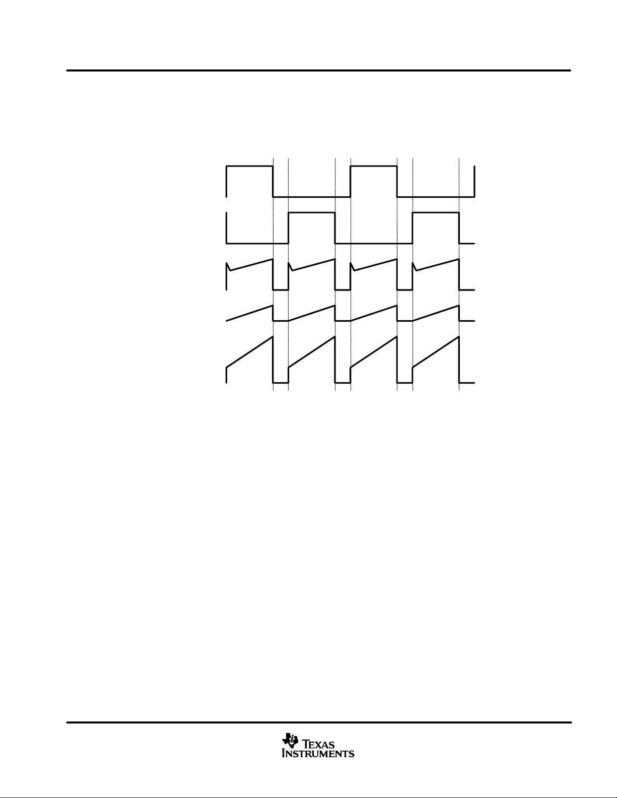
Figure 3 illustrates how the voltage ramp is effectively added to the voltage across the current sense element
V
, to implement slope compensation.
CS
OUTA
OUTB
V
RS
ADDED
RAMP
VO LTA G E
V
,Pin3
CS
UDG--01085
Figure 3. Typical Slope Compensation Waveforms at 80% Duty Cycle
In Figure 3, OUTA and OUTB are shown at a duty cycle of 80%, with the associated voltage VRS across the
current sense resistor of the primary push-pull power MOSFETs. The current flowing out of CS generates the
ramp voltage across the filter resistor R
that is positioned between the power current sense resistor and the
F
CS pin. This voltage is effectively added to VRS to provide slope compensation at VCS, pin 3. A capacitor C
is also recommended to filter the waveform at CS.
F
www.ti.com
9
Page 10

UCC28083, UCC28084, UCC28085, UCC28086
UCC38083, UCC38084, UCC38085, UCC38086
SLUS488D -- SEPTEMBER 2002 -- REVISED AUGUST 2006
layout considerations
To prevent noise problems, bypass VDD to GND with a ceramic capacitor as close to the chip as possible along
with an electrolytic capacitor. A 1-μF decoupling capacitor is recommended.
Use a local ground plane near the small signal pins (CTRL, ISET, CS and RT) of the IC for shielding. Connect
the local ground plane to the GND pin with a single trace. Do not extend the local ground plane under the power
pins (VDD, OUTA, OUTB and GND). Instead, use signal return traces to the GND pin for ground returns on the
side of the integrated circuit with the power pins.
For best performance, keep the timing resistor lead from RT pin (pin 4) to GND (pin 5) as short as possible.
special layout considerations for the TSSOP package
Due to the different pinout and smaller lead pitch of the TSSOP package, special attention must be paid to
minimize noise problems. The pinout is different because the device had to be rotated 90° to fit into the smaller
TSSOP package.
For example, the two output pins are now on opposite sides of the package. The traces should not run under
the package together as they will couple switching noise into analog pins.
Another common problem is when RT and OUTB (pins 6 and 8) are routed together for some distance even
though they are not immediate side by side pins. Because of this, when OUTB rises, a v oltage spike of upto
400 mV can couple into the RT. This spike causes the internal charge current into CT to be turned off
momentarily resulting in lower duty cycle. It is also important that note that the RT pin voltage cannot be
stabilized with a capacitor. The RT pin is just a dc voltage to program the internal CT. Instead, keep the OUTB
and RT runs short and far from each other and follow the printed wiring board layout suggestions above to fix
the problem.
reference design
A reference design is discussed in 50-W Push-Pull Converter Reference D esign Using the UCC38083,TI
Literature Number SLUU135. This design controls a push-pull synchronous rectified topology with input range
of 18 V to 35 V (24 nominal) and 3.3-V output at 15 A. The schematic is shown in Figure 5 and the board layout
for the reference design is s hown in Figure 4. Refer to the document for further details.
10
Figure 4. Reference Design Layout
www.ti.com
Page 11

UCC28083, UCC28084, UCC28085, UCC28086
UCC38083, UCC38084, UCC38085, UCC38086
SLUS488D -- SEPTEMBER 2002 -- REVISED AUGUST 2006
APPLICATION INFORMATION
+ +
3
1
2
1IN42IN
GND
REG_IN
VCC
REG_OUT
2OUT71OUT
8
5
6
+
Figure 5. Reference Design Schematic
www.ti.com
SeeNote2
Note 1. C28, R25, and D12 accelerate the control to the secondary side feedback at start-up and prevent output voltage overshoot.
Note 2. Components used for the UCC38085 only.
11
Page 12

UCC28083, UCC28084, UCC28085, UCC28086
Y
UCC38083, UCC38084, UCC38085, UCC38086
SLUS488D -- SEPTEMBER 2002 -- REVISED AUGUST 2006
TYPICAL CHARACTERISTICS
OSCILLATOR FREQUENCY
vs
TIMING RESISTANCE
1200
1000
800
600
400
Frequency -- kHz
200
0
T=40°C
=6V
V
DD
10 100 1000
RT -- Timing Resistance -- kΩ
T=85°C
VDD=15V
T=25°C
=10V
V
DD
Figure 6
OSCILLATOR FREQUENC
vs
TEMPERATURE
220
RT= 165 kΩ″
=1kΩ
R
F
= 220 kΩ
C
F
=50kΩ
R
SET
--50 50 125
--25 0 25 75 100
Temperature --
°C
Frequency -- kHz
215
210
205
200
195
190
185
180
Figure 7
IDD
vs
OSCILLATOR FREQUENCY, (NO LOAD)
12
10
8
6
IDD -- mA
4
2
0
10 1000
100
Frequency -- kHz
VDD=14V
V
DD
Figure 8
=10V
V
DD
=6V
IDD
vs
OSCILLATOR FREQUENCY, 1 nF LOAD
25
V
DD
=6V
VDD=14V
=10V
100
20
15
V
10
IDD -- mA
5
0
10 1000
DD
Frequency -- kHz
Figure 9
12
www.ti.com
Page 13

UCC28083, UCC28084, UCC28085, UCC28086
UCC38083, UCC38084, UCC38085, UCC38086
SLUS488D -- SEPTEMBER 2002 -- REVISED AUGUST 2006
TYPICAL CHARACTERISTICS
DEADTIME
vs
TIMING RESISTANCE OVER VDD
200
180
160
T=25°C
=6V*
140
120
100
80
Dead Time -- ns
60
40
20
* UCCx8084/6, only
0
10 1000
VDD=14V
T=--40°C
RT -- Timing Resistance -- kΩ
V
DD
100
=6V*
V
DD
T=85°C
V
V
DD
DD
Figure 10
=10V
=14V
DEAD TIME
vs
TEMPERATURE
160
RT= 165 kΩ″
=1kΩ
R
140
120
100
Dead Time -- ns
F
= 220 kΩ
C
F
=50kΩ
R
SET
80
60
40
20
0
--50 125
--25 0 25 75 100
Temperature --
50
°C
Figure 11
CONTROL TO CS OFFSET
vs
TEMPERATURE
2.0
1.8
1.6
V
=0V
50
°C
=0.40V
CS
1.4
1.2
1.0
0.8
-- Control Voltage -- V
0.6
CTRL
V
0.4
0.2
0.0
--50 125
--25 0 25 75 100
Temperature --
V
CS
Figure 12
RAMP HEIGHT
vs
0.6
0.5
0.4
-- V
0.3
PK(cs)
V
0.2
0.1
=25°C
T
A
=10kΩ
R
SET
R
=18kΩ
SET
R
=50kΩ
SET
R
= 100 kΩ
SET
0
015
VDD
5
(OC Clamped)
10
VDD -- Volts
Figure 13
www.ti.com
13
Page 14

UCC28083, UCC28084, UCC28085, UCC28086
UCC38083, UCC38084, UCC38085, UCC38086
SLUS488D -- SEPTEMBER 2002 -- REVISED AUGUST 2006
TYPICAL CHARACTERISTICS
RAMP HEIGHT
vs
RT
0.7
T
=25°C
A
0.6
(OC Clamped)
R
=10kΩ
0.5
0.4
-- V
PK(cs)
0.3
V
0.2
0.1
SET
R
=18kΩ
SET
=50kΩ
R
SET
R
= 100 kΩ
SET
0
RT -- k
100
Ω
10 1000
Figure 14
RAMP HEIGHT
vs
TEMPERATURE
0.6
=10kΩ
R
SET
0.5
R
=18kΩ
0.4
-- V
0.3
PK(cs)
V
0.2
0.1
0.0
SET
=50kΩ
R
SET
R
= 100 kΩ
SET
--50 125
--25 0 50 75 100
Temperature --
(OC Clamped)
25
°C
Figure 15
SOFT START
vs
TEMPERATURE
6
UCCx8083 AND UCCx8084
5
4
3
2
Soft Start Internal -- ms
1
0
--50 125
25
0--25 50 75 100
Temperature --
°C
Figure 16
SOFT START
vs
TEMPERATURE
100
UCCx8085 AND UCCx8086
95
90
85
80
75
70
Soft Start Internal -- μs
65
60
55
50
--50 125
25
Temperature --
50 75 1000-- 2 5
°C
Figure 17
14
www.ti.com
Page 15

UCC28083, UCC28084, UCC28085, UCC28086
UCC38083, UCC38084, UCC38085, UCC38086
SLUS488D -- SEPTEMBER 2002 -- REVISED AUGUST 2006
TYPICAL CHARACTERISTICS
CS TO OUTX DELAY TIME
vs
TEMPERATURE
150
140
130
120
110
100
90
CS Prop Delay -- ns
80
70
60
50
--50 125
Temperature --
25
50 75 1000-- 2 5
°C
Figure 18
RELATED PRODUCTS
UCC3808, 8-Pin Low Power Current Mode Push-Pull PWM, (SLUS168)
UCC3808A, 8-Pin Low-Power Current-Mode Push-Pull PWM, (SLUS456)
UCC3806, Low Power, Dual Output, Current Mode PWM Controller, (SLUS272)
Table 1. 8-Pin Push-Pull PWM Controller Family Feature Comparison
Part Number UVLO On UVLO Off
UCC38083 12.5 V 8.3 V Yes No Yes Yes
UCC38084 4.3 V 4.1 V Yes No Yes Yes
UCC38085 12.5 V 8.3 V Yes No Yes No
UCC38086 4.3 V 4.1 V Yes No Yes No
UCC3808A--1 12.5 V 8.3 V Yes Yes No Yes
UCC3808A--2 4.3 V 4.1 V Yes Yes No Yes
UCC3808--1 12.5 V 8.3 V No Yes No Yes
UCC3808--2 4.3 V 4.1 V No Ye s No Ye s
CS
Discharge FET
Error
Amplifier
Programmable
Slope
Compensation
Internal
Softstart
www.ti.com
15
Page 16

UCC28083, UCC28084, UCC28085, UCC28086
UCC38083, UCC38084, UCC38085, UCC38086
SLUS488D -- SEPTEMBER 2002 -- REVISED AUGUST 2006
MECHANICAL DATA
D (R-PDSO-G**) PLASTIC SMALL -OUTLINE PACKAGE
8PINSSHOWN
8 5
1 4
A
0.069 (1,75) MAX
0.020 (0,51)
0.014 (0,35)
0.157 (4,00)
0.150 (3,81)
0.010 (0,25)
0.004 (0,10)
0.244 (6,20)
0.228 (5,80)
0.010 (0,25)0.050 (1,27)
0.008 (0,20) NOM
Gage Plane
0.010 (0,25)
0°-- 8 °
0.044 (1,12)
0.016 (0,40)
Seating Plane
0.004 (0,10)
PINS **
DIM
AMAX
AMIN
NOTES: A. All linear dimensions are in inches (millimeters).
B. This drawing is subject to change without notice.
C. Body dimensions do not include mold flash or protrusion, not to exceed 0.006 (0,15).
D. Falls within JEDEC MS-012
8
0.197
(5,00)
0.189
(4,80)
14
0.344
(8,75)
0.337
(8,55)
16
0.394
(10,00)
0.386
(9,80)
4040047/E 09/01
16
www.ti.com
Page 17

UCC28083, UCC28084, UCC28085, UCC28086
f
/
/
UCC38083, UCC38084, UCC38085, UCC38086
SLUS488D -- SEPTEMBER 2002 -- REVISED AUGUST 2006
MECHANICAL DATA
P(PDIP) PLASTIC DUAL-IN-LINE
0.400 (10,60)
0.355 (9,02)
8
5
0.260 (6,60)
0.240 (6,10)
1
0.021 (0,53)
0.015 (0,38)
NOTES: A. All linear dimensions are in inches (millimeters).
B. This drawing is subject to change without notice.
C. Falls within JEDEC MS-001
4
0.070 (1,78) MAX
0.020 (0,51) MIN
0.200 (5,08) MAX
0.125 (3,18) MIN
0.100 (2,54)
0.010 (0,25)
Seating Plane
M
0.325 (8,26)
0.300 (7,62)
0.015 (0,38)
Gage Plane
0.010 (0,25) NOM
0.430 (10,92)
MAX
4040082/D 05/98
For the latest package in
ormation, go to http:
www.ti.com/sc/docs/package/pkg_info.htm
www.ti.com
17
Page 18

UCC28083, UCC28084, UCC28085, UCC28086
f
/
/
UCC38083, UCC38084, UCC38085, UCC38086
SLUS488D -- SEPTEMBER 2002 -- REVISED AUGUST 2006
MECHANICAL DATA
PW (R-PDSO-G**) PLASTIC SMALL-OUTLINE
PACKAGE
14 PINS SHOWN
0,65
1,20 MAX
14
0,30
0,19
8
4,50
4,30
PINS **
7
0,15
0,05
Seating Plane
8
14
1
A
DIM
0,10
6,60
6,20
M
0,10
0,15 NOM
0°-- 8 °
2016
Gage Plane
24
0,25
0,75
0,50
28
AMAX
AMIN
NOTES:A. All linear dimensions are in millimeters.
B. This drawing is subject to change without notice.
C. Body dimensions do not include mold flash or protrusion not to exceed 0,15.
D. Falls within JEDEC MO-153
For the latest package in
18
ormation, go to http:
3,10
2,90
www.ti.com/sc/docs/package/pkg_info.htm
5,10
4,90
www.ti.com
5,10
4,90
6,60
6,40
7,90
7,70
9,80
9,60
4040064/F 01/97
Page 19

PACKAGE OPTION ADDENDUM
www.ti.com
PACKAGING INFORMATION
Orderable Device Status
UCC28083D ACTIVE SOIC D 8 75 Green (RoHS &
UCC28083DG4 ACTIVE SOIC D 8 75 Green (RoHS &
UCC28083DR ACTIVE SOIC D 8 2500 Green (RoHS &
UCC28083DRG4 ACTIVE SOIC D 8 2500 Green (RoHS &
UCC28083P ACTIVE PDIP P 8 50 Green (RoHS &
UCC28083PG4 ACTIVE PDIP P 8 50 Green (RoHS &
UCC28083PW ACTIVE TSSOP PW 8 150 Green (RoHS &
UCC28083PWG4 ACTIVE TSSOP PW 8 150 Green (RoHS &
UCC28083PWR ACTIVE TSSOP PW 8 2000 Green (RoHS &
UCC28083PWRG4 ACTIVE TSSOP PW 8 2000 Green (RoHS &
UCC28084D ACTIVE SOIC D 8 75 Green (RoHS &
UCC28084DG4 ACTIVE SOIC D 8 75 Green (RoHS &
UCC28084DR ACTIVE SOIC D 8 2500 Green (RoHS &
UCC28084DRG4 ACTIVE SOIC D 8 2500 Green (RoHS &
UCC28084P ACTIVE PDIP P 8 50 Green (RoHS &
UCC28084PG4 ACTIVE PDIP P 8 50 Green (RoHS &
UCC28084PW ACTIVE TSSOP PW 8 150 Green (RoHS &
UCC28084PWG4 ACTIVE TSSOP PW 8 150 Green (RoHS &
UCC28084PWR ACTIVE TSSOP PW 8 2000 Green (RoHS &
UCC28084PWRG4 ACTIVE TSSOP PW 8 2000 Green (RoHS &
UCC28085D ACTIVE SOIC D 8 75 Green (RoHS &
UCC28085DG4 ACTIVE SOIC D 8 75 Green (RoHS &
UCC28085DR ACTIVE SOIC D 8 2500 Green (RoHS &
UCC28085DRG4 ACTIVE SOIC D 8 2500 Green (RoHS &
UCC28085P ACTIVE PDIP P 8 50 Green (RoHS &
(1)
Package
Type
Package
Drawing
Pins Package
Qty
Eco Plan
no Sb/Br)
no Sb/Br)
no Sb/Br)
no Sb/Br)
no Sb/Br)
no Sb/Br)
no Sb/Br)
no Sb/Br)
no Sb/Br)
no Sb/Br)
no Sb/Br)
no Sb/Br)
no Sb/Br)
no Sb/Br)
no Sb/Br)
no Sb/Br)
no Sb/Br)
no Sb/Br)
no Sb/Br)
no Sb/Br)
no Sb/Br)
no Sb/Br)
no Sb/Br)
no Sb/Br)
no Sb/Br)
(2)
Lead/Ball Finish MSL Peak Temp
CU NIPDAU Level-2-260C-1 YEAR
CU NIPDAU Level-2-260C-1 YEAR
CU NIPDAU Level-2-260C-1 YEAR
CU NIPDAU Level-2-260C-1 YEAR
CU NIPDAU N / A for Pkg Type
CU NIPDAU N / A for Pkg Type
CU NIPDAU Level-2-260C-1 YEAR
CU NIPDAU Level-2-260C-1 YEAR
CU NIPDAU Level-2-260C-1 YEAR
CU NIPDAU Level-2-260C-1 YEAR
CU NIPDAU Level-2-260C-1 YEAR
CU NIPDAU Level-2-260C-1 YEAR
CU NIPDAU Level-2-260C-1 YEAR
CU NIPDAU Level-2-260C-1 YEAR
CU NIPDAU N / A for Pkg Type
CU NIPDAU N / A for Pkg Type
CU NIPDAU Level-2-260C-1 YEAR
CU NIPDAU Level-2-260C-1 YEAR
CU NIPDAU Level-2-260C-1 YEAR
CU NIPDAU Level-2-260C-1 YEAR
CU NIPDAU Level-2-260C-1 YEAR
CU NIPDAU Level-2-260C-1 YEAR
CU NIPDAU Level-2-260C-1 YEAR
CU NIPDAU Level-2-260C-1 YEAR
CU NIPDAU N / A for Pkg Type
3-Mar-2008
(3)
Addendum-Page 1
Page 20

PACKAGE OPTION ADDENDUM
www.ti.com
Orderable Device Status
(1)
Package
Type
Package
Drawing
Pins Package
Qty
Eco Plan
(2)
UCC28085PG4 ACTIVE PDIP P 8 50 Green (RoHS &
no Sb/Br)
UCC28085PW ACTIVE TSSOP PW 8 150 Green (RoHS &
no Sb/Br)
UCC28085PWG4 ACTIVE TSSOP PW 8 150 Green (RoHS &
no Sb/Br)
UCC28085PWR ACTIVE TSSOP PW 8 2000 Green (RoHS &
no Sb/Br)
UCC28085PWRG4 ACTIVE TSSOP PW 8 2000 Green (RoHS &
no Sb/Br)
UCC28086D ACTIVE SOIC D 8 75 Green (RoHS &
no Sb/Br)
UCC28086DG4 ACTIVE SOIC D 8 75 Green (RoHS &
no Sb/Br)
UCC28086DR ACTIVE SOIC D 8 2500 Green (RoHS &
no Sb/Br)
UCC28086DRG4 ACTIVE SOIC D 8 2500 Green (RoHS &
no Sb/Br)
UCC28086P ACTIVE PDIP P 8 50 Green (RoHS &
no Sb/Br)
UCC28086PG4 ACTIVE PDIP P 8 50 Green (RoHS &
no Sb/Br)
UCC28086PW ACTIVE TSSOP PW 8 150 Green (RoHS &
no Sb/Br)
UCC28086PWG4 ACTIVE TSSOP PW 8 150 Green (RoHS &
no Sb/Br)
UCC28086PWR ACTIVE TSSOP PW 8 2000 Green (RoHS &
no Sb/Br)
UCC28086PWRG4 ACTIVE TSSOP PW 8 2000 Green (RoHS &
no Sb/Br)
UCC38083D ACTIVE SOIC D 8 75 Green (RoHS &
no Sb/Br)
UCC38083DG4 ACTIVE SOIC D 8 75 Green (RoHS &
no Sb/Br)
UCC38083DR ACTIVE SOIC D 8 2500 Green (RoHS &
no Sb/Br)
UCC38083DRG4 ACTIVE SOIC D 8 2500 Green (RoHS &
no Sb/Br)
UCC38083P ACTIVE PDIP P 8 50 Green (RoHS &
no Sb/Br)
UCC38083PG4 ACTIVE PDIP P 8 50 Green (RoHS &
no Sb/Br)
UCC38083PW ACTIVE TSSOP PW 8 150 Green (RoHS &
no Sb/Br)
UCC38083PWG4 ACTIVE TSSOP PW 8 150 Green (RoHS &
no Sb/Br)
UCC38083PWR ACTIVE TSSOP PW 8 2000 Green (RoHS &
no Sb/Br)
UCC38083PWRG4 ACTIVE TSSOP PW 8 2000 Green (RoHS &
no Sb/Br)
UCC38084D ACTIVE SOIC D 8 75 Green (RoHS &
no Sb/Br)
3-Mar-2008
Lead/Ball Finish MSL Peak Temp
CU NIPDAU N / A for Pkg Type
Call TI Level-2-260C-1 YEAR
Call TI Level-2-260C-1 YEAR
CU NIPDAU Level-2-260C-1 YEAR
CU NIPDAU Level-2-260C-1 YEAR
CU NIPDAU Level-2-260C-1 YEAR
CU NIPDAU Level-2-260C-1 YEAR
CU NIPDAU Level-2-260C-1 YEAR
CU NIPDAU Level-2-260C-1 YEAR
CU NIPDAU N / A for Pkg Type
CU NIPDAU N / A for Pkg Type
CU NIPDAU Level-2-260C-1 YEAR
CU NIPDAU Level-2-260C-1 YEAR
CU NIPDAU Level-2-260C-1 YEAR
CU NIPDAU Level-2-260C-1 YEAR
CU NIPDAU Level-2-260C-1 YEAR
CU NIPDAU Level-2-260C-1 YEAR
CU NIPDAU Level-2-260C-1 YEAR
CU NIPDAU Level-2-260C-1 YEAR
CU NIPDAU N / A for Pkg Type
CU NIPDAU N / A for Pkg Type
CU NIPDAU Level-2-260C-1 YEAR
CU NIPDAU Level-2-260C-1 YEAR
CU NIPDAU Level-2-260C-1 YEAR
CU NIPDAU Level-2-260C-1 YEAR
CU NIPDAU Level-2-260C-1 YEAR
(3)
Addendum-Page 2
Page 21

PACKAGE OPTION ADDENDUM
www.ti.com
Orderable Device Status
(1)
Package
Type
Package
Drawing
Pins Package
Qty
Eco Plan
(2)
UCC38084DG4 ACTIVE SOIC D 8 75 Green (RoHS &
no Sb/Br)
UCC38084DR ACTIVE SOIC D 8 2500 Green (RoHS &
no Sb/Br)
UCC38084DRG4 ACTIVE SOIC D 8 2500 Green (RoHS &
no Sb/Br)
UCC38084P ACTIVE PDIP P 8 50 Green (RoHS &
no Sb/Br)
UCC38084PG4 ACTIVE PDIP P 8 50 Green (RoHS &
no Sb/Br)
UCC38084PW ACTIVE TSSOP PW 8 150 Green (RoHS &
no Sb/Br)
UCC38084PWG4 ACTIVE TSSOP PW 8 150 Green (RoHS &
no Sb/Br)
UCC38084PWR ACTIVE TSSOP PW 8 2000 Green (RoHS &
no Sb/Br)
UCC38084PWRG4 ACTIVE TSSOP PW 8 2000 Green (RoHS &
no Sb/Br)
UCC38085D ACTIVE SOIC D 8 75 Green (RoHS &
no Sb/Br)
UCC38085DG4 ACTIVE SOIC D 8 75 Green (RoHS &
no Sb/Br)
UCC38085DR ACTIVE SOIC D 8 2500 Green (RoHS &
no Sb/Br)
UCC38085DRG4 ACTIVE SOIC D 8 2500 Green (RoHS &
no Sb/Br)
UCC38085P ACTIVE PDIP P 8 50 Green (RoHS &
no Sb/Br)
UCC38085PG4 ACTIVE PDIP P 8 50 Green (RoHS &
no Sb/Br)
UCC38085PW ACTIVE TSSOP PW 8 150 Green (RoHS &
no Sb/Br)
UCC38085PWG4 ACTIVE TSSOP PW 8 150 Green (RoHS &
no Sb/Br)
UCC38085PWR ACTIVE TSSOP PW 8 2000 Green (RoHS &
no Sb/Br)
UCC38085PWRG4 ACTIVE TSSOP PW 8 2000 Green (RoHS &
no Sb/Br)
UCC38086D ACTIVE SOIC D 8 75 Green (RoHS &
no Sb/Br)
UCC38086DG4 ACTIVE SOIC D 8 75 Green (RoHS &
no Sb/Br)
UCC38086DR ACTIVE SOIC D 8 2500 Green (RoHS &
no Sb/Br)
UCC38086DRG4 ACTIVE SOIC D 8 2500 Green (RoHS &
no Sb/Br)
UCC38086P ACTIVE PDIP P 8 50 Green (RoHS &
no Sb/Br)
UCC38086PG4 ACTIVE PDIP P 8 50 Green (RoHS &
no Sb/Br)
UCC38086PW ACTIVE TSSOP PW 8 150 Green (RoHS &
no Sb/Br)
3-Mar-2008
Lead/Ball Finish MSL Peak Temp
CU NIPDAU Level-2-260C-1 YEAR
CU NIPDAU Level-2-260C-1 YEAR
CU NIPDAU Level-2-260C-1 YEAR
CU NIPDAU N / A for Pkg Type
CU NIPDAU N / A for Pkg Type
CU NIPDAU Level-2-260C-1 YEAR
CU NIPDAU Level-2-260C-1 YEAR
CU NIPDAU Level-2-260C-1 YEAR
CU NIPDAU Level-2-260C-1 YEAR
CU NIPDAU Level-2-260C-1 YEAR
CU NIPDAU Level-2-260C-1 YEAR
CU NIPDAU Level-2-260C-1 YEAR
CU NIPDAU Level-2-260C-1 YEAR
CU NIPDAU N / A for Pkg Type
CU NIPDAU N / A for Pkg Type
CU NIPDAU Level-2-260C-1 YEAR
CU NIPDAU Level-2-260C-1 YEAR
CU NIPDAU Level-2-260C-1 YEAR
CU NIPDAU Level-2-260C-1 YEAR
CU NIPDAU Level-2-260C-1 YEAR
CU NIPDAU Level-2-260C-1 YEAR
Call TI Level-2-260C-1 YEAR
Call TI Level-2-260C-1 YEAR
CU NIPDAU N / A for Pkg Type
CU NIPDAU N / A for Pkg Type
CU NIPDAU Level-2-260C-1 YEAR
(3)
Addendum-Page 3
Page 22

PACKAGE OPTION ADDENDUM
www.ti.com
Orderable Device Status
(1)
Package
Type
Package
Drawing
Pins Package
Qty
Eco Plan
(2)
UCC38086PWG4 ACTIVE TSSOP PW 8 150 Green (RoHS &
Lead/Ball Finish MSL Peak Temp
CU NIPDAU Level-2-260C-1 YEAR
3-Mar-2008
(3)
no Sb/Br)
UCC38086PWR ACTIVE TSSOP PW 8 2000 Green (RoHS &
CU NIPDAU Level-2-260C-1 YEAR
no Sb/Br)
UCC38086PWRG4 ACTIVE TSSOP PW 8 2000 Green (RoHS &
CU NIPDAU Level-2-260C-1 YEAR
no Sb/Br)
(1)
The marketing status values are defined as follows:
ACTIVE: Product device recommended for new designs.
LIFEBUY: TI has announced that the device will be discontinued, and a lifetime-buy period is in effect.
NRND: Not recommended for new designs. Device is in production to support existing customers, but TI does not recommend using this part in
a new design.
PREVIEW: Device has been announced but is not in production. Samples may or may not be available.
OBSOLETE: TI has discontinued the production of the device.
(2)
Eco Plan - The planned eco-friendly classification: Pb-Free (RoHS), Pb-Free (RoHS Exempt), or Green (RoHS & no Sb/Br) - please check
http://www.ti.com/productcontent for the latest availability information and additional product content details.
TBD: The Pb-Free/Green conversion plan has not been defined.
Pb-Free (RoHS): TI's terms "Lead-Free" or "Pb-Free" mean semiconductor products that are compatible with the current RoHS requirements
for all 6 substances, including the requirement that lead not exceed 0.1% by weight in homogeneous materials. Where designed to be soldered
at high temperatures, TI Pb-Free products are suitable for use in specified lead-free processes.
Pb-Free (RoHS Exempt): This component has a RoHS exemption for either 1) lead-based flip-chip solder bumps used between the die and
package, or 2) lead-based die adhesive used between the die and leadframe. The component is otherwise considered Pb-Free (RoHS
compatible) as defined above.
Green (RoHS & no Sb/Br): TI defines "Green" to mean Pb-Free (RoHS compatible), and free of Bromine (Br) and Antimony (Sb) based flame
retardants (Br or Sb do not exceed 0.1% by weight in homogeneous material)
(3)
MSL, Peak Temp. -- The Moisture Sensitivity Level rating according to the JEDEC industry standard classifications, and peak solder
temperature.
Important Information and Disclaimer:The information provided on this page represents TI's knowledge and belief as of the date that it is
provided. TI bases its knowledge and belief on information provided by third parties, and makes no representation or warranty as to the
accuracy of such information. Efforts are underway to better integrate information from third parties. TI has taken and continues to take
reasonable steps to provide representative and accurate information but may not have conducted destructive testing or chemical analysis on
incoming materials and chemicals. TI and TI suppliers consider certain information to be proprietary, and thus CAS numbers and other limited
information may not be available for release.
In no event shall TI's liability arising out of such information exceed the total purchase price of the TI part(s) at issue in this document sold by TI
to Customer on an annual basis.
Addendum-Page 4
Page 23
PACKAGE MATERIALS INFORMATION
www.ti.com
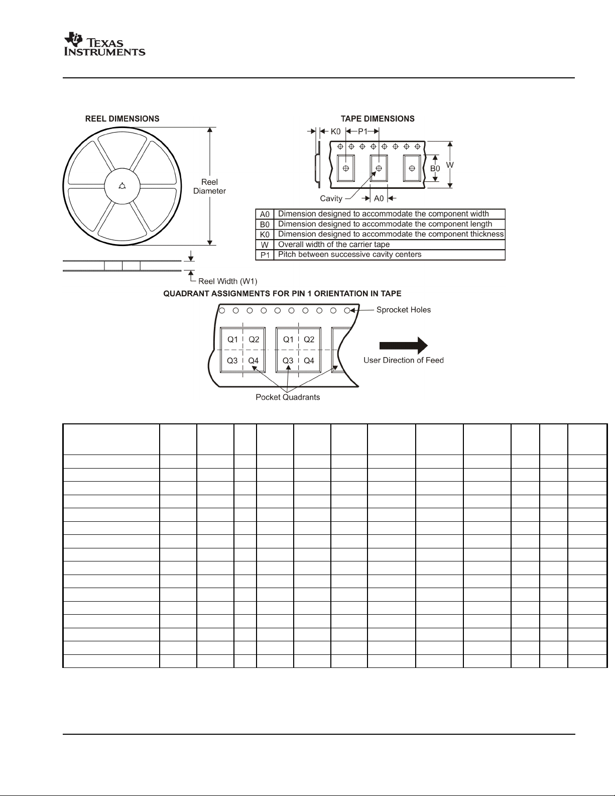
TAPE AND REEL INFORMATION
11-Mar-2008
*All dimensions are nominal
Device Package
Type
UCC28083DR SOIC D 8 2500 330.0 12.4 6.4 5.2 2.1 8.0 12.0 Q1
UCC28083PWR TSSOP PW 8 2000 330.0 12.4 7.0 3.6 1.6 8.0 12.0 Q1
UCC28084DR SOIC D 8 2500 330.0 12.4 6.4 5.2 2.1 8.0 12.0 Q1
UCC28084PWR TSSOP PW 8 2000 330.0 12.4 7.0 3.6 1.6 8.0 12.0 Q1
UCC28085DR SOIC D 8 2500 330.0 12.4 6.4 5.2 2.1 8.0 12.0 Q1
UCC28085PWR TSSOP PW 8 2000 330.0 12.4 7.0 3.6 1.6 8.0 12.0 Q1
UCC28086DR SOIC D 8 2500 330.0 12.4 6.4 5.2 2.1 8.0 12.0 Q1
UCC28086PWR TSSOP PW 8 2000 330.0 12.4 7.0 3.6 1.6 8.0 12.0 Q1
UCC38083DR SOIC D 8 2500 330.0 12.4 6.4 5.2 2.1 8.0 12.0 Q1
UCC38083PWR TSSOP PW 8 2000 330.0 12.4 7.0 3.6 1.6 8.0 12.0 Q1
UCC38084DR SOIC D 8 2500 330.0 12.4 6.4 5.2 2.1 8.0 12.0 Q1
UCC38084PWR TSSOP PW 8 2000 330.0 12.4 7.0 3.6 1.6 8.0 12.0 Q1
UCC38085DR SOIC D 8 2500 330.0 12.4 6.4 5.2 2.1 8.0 12.0 Q1
UCC38085PWR TSSOP PW 8 2000 330.0 12.4 7.0 3.6 1.6 8.0 12.0 Q1
UCC38086DR SOIC D 8 2500 330.0 12.4 6.4 5.2 2.1 8.0 12.0 Q1
UCC38086PWR TSSOP PW 8 2000 330.0 12.4 7.0 3.6 1.6 8.0 12.0 Q1
Package
Drawing
Pins SPQ Reel
Diameter
(mm)
Reel
Width
W1 (mm)
A0 (mm) B0 (mm) K0 (mm) P1
(mm)W(mm)
Pin1
Quadrant
Pack Materials-Page 1
Page 24
PACKAGE MATERIALS INFORMATION
www.ti.com
11-Mar-2008
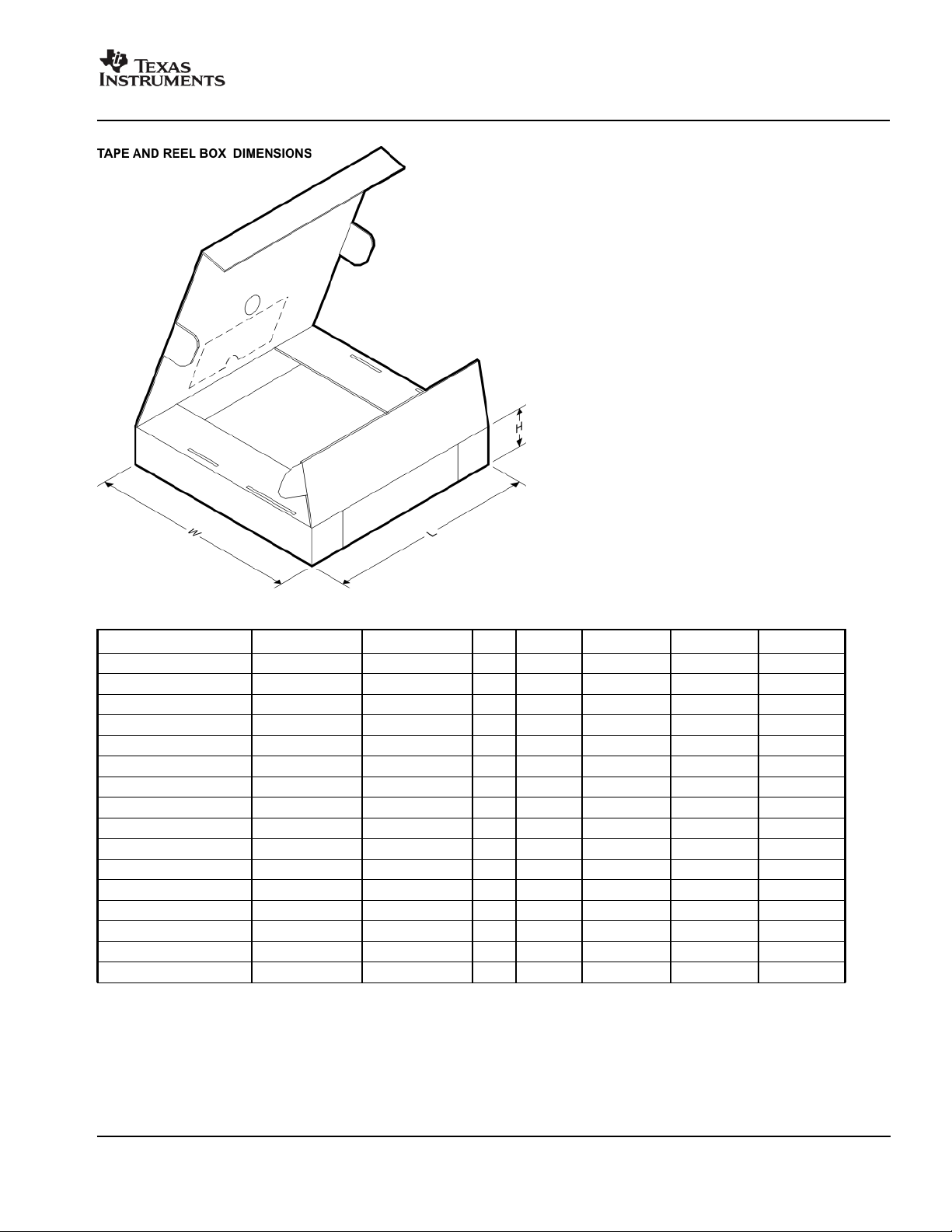
*All dimensions are nominal
Device Package Type Package Drawing Pins SPQ Length (mm) Width (mm) Height (mm)
UCC28083DR SOIC D 8 2500 346.0 346.0 29.0
UCC28083PWR TSSOP PW 8 2000 346.0 346.0 29.0
UCC28084DR SOIC D 8 2500 346.0 346.0 29.0
UCC28084PWR TSSOP PW 8 2000 346.0 346.0 29.0
UCC28085DR SOIC D 8 2500 346.0 346.0 29.0
UCC28085PWR TSSOP PW 8 2000 346.0 346.0 29.0
UCC28086DR SOIC D 8 2500 346.0 346.0 29.0
UCC28086PWR TSSOP PW 8 2000 346.0 346.0 29.0
UCC38083DR SOIC D 8 2500 346.0 346.0 29.0
UCC38083PWR TSSOP PW 8 2000 346.0 346.0 29.0
UCC38084DR SOIC D 8 2500 346.0 346.0 29.0
UCC38084PWR TSSOP PW 8 2000 346.0 346.0 29.0
UCC38085DR SOIC D 8 2500 346.0 346.0 29.0
UCC38085PWR TSSOP PW 8 2000 346.0 346.0 29.0
UCC38086DR SOIC D 8 2500 346.0 346.0 29.0
UCC38086PWR TSSOP PW 8 2000 346.0 346.0 29.0
Pack Materials-Page 2
Page 25

MECHANICAL DATA
MTSS001C – JANUARY 1995 – REVISED FEBRUARY 1999
PW (R-PDSO-G**) PLASTIC SMALL-OUTLINE PACKAGE
14 PINS SHOWN
0,65
1,20 MAX
14
0,30
0,19
8
4,50
4,30
PINS **
7
0,15
0,05
Seating Plane
8
14
1
A
DIM
0,10
6,60
6,20
0,10
M
0,15 NOM
Gage Plane
0,25
0°–8°
2016
24
28
0,75
0,50
A MAX
A MIN
NOTES: A. All linear dimensions are in millimeters.
B. This drawing is subject to change without notice.
C. Body dimensions do not include mold flash or protrusion not to exceed 0,15.
D. Falls within JEDEC MO-153
3,10
2,90
5,10
4,90
5,10
4,90
6,60
6,40
7,90
7,70
9,80
9,60
4040064/F 01/97
POST OFFICE BOX 655303 • DALLAS, TEXAS 75265
Page 26

Page 27
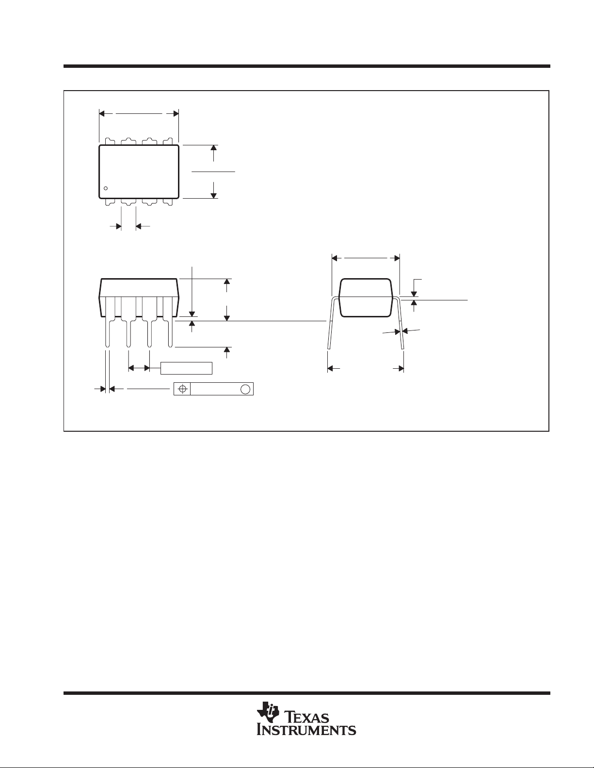
MECHANICAL DATA
MPDI001A – JANUARY 1995 – REVISED JUNE 1999
P (R-PDIP-T8) PLASTIC DUAL-IN-LINE
0.400 (10,60)
0.355 (9,02)
8
5
0.260 (6,60)
0.240 (6,10)
1
0.021 (0,53)
0.015 (0,38)
NOTES: A. All linear dimensions are in inches (millimeters).
B. This drawing is subject to change without notice.
C. Falls within JEDEC MS-001
4
0.070 (1,78) MAX
0.020 (0,51) MIN
0.200 (5,08) MAX
0.125 (3,18) MIN
0.100 (2,54)
0.010 (0,25)
Seating Plane
M
0.325 (8,26)
0.300 (7,62)
0.015 (0,38)
Gage Plane
0.010 (0,25) NOM
0.430 (10,92)
MAX
4040082/D 05/98
For the latest package information, go to http://www.ti.com/sc/docs/package/pkg_info.htm
POST OFFICE BOX 655303 • DALLAS, TEXAS 75265
Page 28

IMPORTANT NOTICE
Texas Instruments Incorporated and its subsidiaries (TI) reserve the right to make corrections, modifications, enhancements, improvements,
and other changes to its products and services at any time and to discontinue any product or service without notice. Customers should
obtain the latest relevant information before placing orders and should verify that such information is current and complete. All products are
sold subject to TI’s terms and conditions of sale supplied at the time of order acknowledgment.
TI warrants performance of its hardware products to the specifications applicable at the time of sale in accordance with TI’s standard
warranty. Testing and other quality control techniques are used to the extent TI deems necessary to support this warranty. Except where
mandated by government requirements, testing of all parameters of each product is not necessarily performed.
TI assumes no liability for applications assistance or customer product design. Customers are responsible for their products and
applications using TI components. To minimize the risks associated with customer products and applications, customers should provide
adequate design and operating safeguards.
TI does not warrant or represent that any license, either express or implied, is granted under any TI patent right, copyright, mask work right,
or other TI intellectual property right relating to any combination, machine, or process in which TI products or services are used. Information
published by TI regarding third-party products or services does not constitute a license from TI to use such products or services or a
warranty or endorsement thereof. Use of such information may require a license from a third party under the patents or other intellectual
property of the third party, or a license from TI under the patents or other intellectual property of TI.
Reproduction of TI information in TI data books or data sheets is permissible only if reproduction is without alteration and is accompanied
by all associated warranties, conditions, limitations, and notices. Reproduction of this information with alteration is an unfair and deceptive
business practice. TI is not responsible or liable for such altered documentation. Information of third parties may be subject to additional
restrictions.
Resale of TI products or services with statements different from or beyond the parameters stated by TI for that product or service voids all
express and any implied warranties for the associated TI product or service and is an unfair and deceptive business practice. TI is not
responsible or liable for any such statements.
TI products are not authorized for use in safety-critical applications (such as life support) where a failure of the TI product would reasonably
be expected to cause severe personal injury or death, unless officers of the parties have executed an agreement specifically governing
such use. Buyers represent that they have all necessary expertise in the safety and regulatory ramifications of their applications, and
acknowledge and agree that they are solely responsible for all legal, regulatory and safety-related requirements concerning their products
and any use of TI products in such safety-critical applications, notwithstanding any applications-related information or support that may be
provided by TI. Further, Buyers must fully indemnify TI and its representatives against any damages arising out of the use of TI products in
such safety-critical applications.
TI products are neither designed nor intended for use in military/aerospace applications or environments unless the TI products are
specifically designated by TI as military-grade or "enhanced plastic." Only products designated by TI as military-grade meet military
specifications. Buyers acknowledge and agree that any such use of TI products which TI has not designated as military-grade is solely at
the Buyer's risk, and that they are solely responsible for compliance with all legal and regulatory requirements in connection with such use.
TI products are neither designed nor intended for use in automotive applications or environments unless the specific TI products are
designated by TI as compliant with ISO/TS 16949 requirements. Buyers acknowledge and agree that, if they use any non-designated
products in automotive applications, TI will not be responsible for any failure to meet such requirements.
Following are URLs where you can obtain information on other Texas Instruments products and application solutions:
Products Applications
Amplifiers amplifier.ti.com Audio www.ti.com/audio
Data Converters dataconverter.ti.com Automotive www.ti.com/automotive
DSP dsp.ti.com Broadband www.ti.com/broadband
Clocks and Timers www.ti.com/clocks Digital Control www.ti.com/digitalcontrol
Interface interface.ti.com Medical www.ti.com/medical
Logic logic.ti.com Military www.ti.com/military
Power Mgmt power.ti.com Optical Networking www.ti.com/opticalnetwork
Microcontrollers microcontroller.ti.com Security www.ti.com/security
RFID www.ti-rfid.com Telephony www.ti.com/telephony
RF/IF and ZigBee® Solutions www.ti.com/lprf Video & Imaging www.ti.com/video
Mailing Address: Texas Instruments, Post Office Box 655303, Dallas, Texas 75265
Copyright © 2008, Texas Instruments Incorporated
Wireless www.ti.com/wireless
 Loading...