

Texas Instruments UCC3807N-3, UCC3807N-2, UCC3807N-1, UCC3807DTR-3, UCC3807DTR-1 Datasheet
...
Programmable Maximum Duty Cycle PWM Controller
UCC1807-1/-2/-3
UCC2807-1/-2/-3
UCC3807-1/-2/-3
FEATURES
• User Programmable
Maximum PWM
Duty Cycle
• 100µA Startup Current
• Operation to 1MHz
• Internal Full Cycle
Soft Start
• Internal Leading Edge
Blanking of Current
Sense Signal
• 1 Amp Totem Pole
Output
DESCRIPTION
The UCC3807 family of high speed, low power integrated circuits contains all of the
control and drive circuitry required for off-line and DC-to-DC fixed frequency current
mode switching power supplies with minimal external parts count.
These devices are similar to the UCC3800 family, but with the added feature of a
user programmable maximum duty cycle.Oscillator frequency and maximum duty
cycle are programmed with two resistors and a capacitor.The UCC3807 family also
features internal full cycle soft start and internal leading edge blanking of the current sense input.
The UCC3807 family offers a variety of package options, temperature range
options, and choice of critical voltage levels.The family has UVLO thresholds and
hysteresis levels for off-line and battery powered systems. Thresholds are shown in
the table below.
6/97
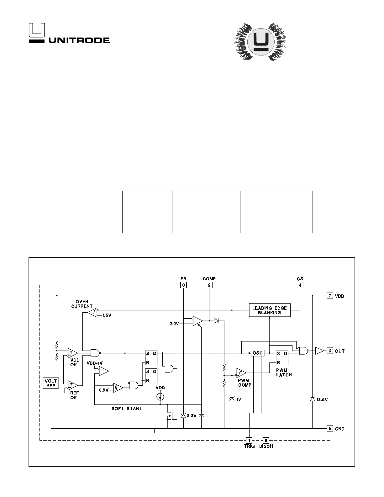
BLOCK DIAGRAM
Part Number Turn-on Threshold Turn-off Threshold
UCCx807-1 7.2V 6.9V
UCCx807-2 12.5V 8.3V
UCCx807-3 4.3V 4.1V
UDG-95001-1
2
UCC1807-1/-2/-3
UCC2807-1/-2/-3
UCC3807-1/-2/-3
ABSOLUTE MAXIMUM RATINGS
Supply Voltage (IDD ≤ 10mA) . . . . . . . . . . . . . . . . . . . . . . .13.5V
Supply Current . . . . . . . . . . . . . . . . . . . . . . . . . . . . . . . . .30mA
OUT Current . . . . . . . . . . . . . . . . . . . . . . . . . . . . . . . . . . . .±1A
Analog Inputs (FB, CS) . . . . . . . . . . . . .−0.3V to (VDD + 0.3V)
Power Dissipation at TA +25°C (N or J packages) . . . . . . . .1W
Power Dissipation at TA +25°C (D package) . . . . . . . . . .0.65W
Storage Temperature . . . . . . . . . . . . . . . . . . . .−65°C to +150°C
Junction Temperature . . . . . . . . . . . . . . . . . . .−65°C to +150°C
Lead Temperature (Soldering, 10 sec.) . . . . . . . . . . . . .+300°C
All currents are positive into, negative out of the specified terminal.
Consult Packaging Section of Databook for thermal limitations
and considerations of packages.
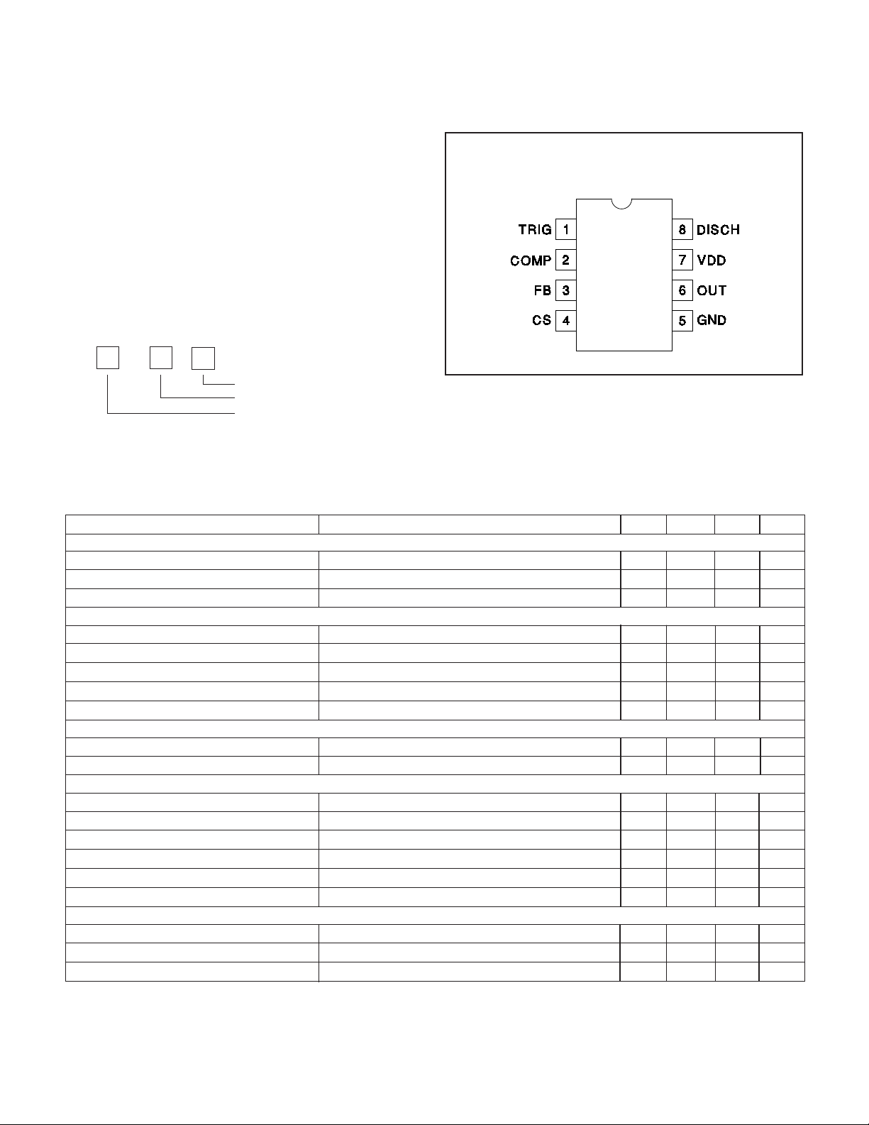
CONNECTION DIAGRAM
DIL-8,SOIC-8 (Top View)
J or N,D Packages
PARAMETER TEST CONDITION MIN TYP MAX UNITS
Oscillator Section
Frequency 175 202 228 kHz
Temperature Stability (Note 5) 2.5 %
Amplitude (Note 1) 1/3VDD V
Error Amplifier Section
Input Voltage COMP = 2.0V 1.95 2.00 2.05 V
Input Bias Current −1 1 µA
Open Loop Voltage Gain 60 80 dB
COMP Sink Current FB = 2.2V, COMP = 1.0V 0.3 2.5 mA
COMP Source Current FB = 1.3V, COMP = 4.0V −0.2 −0.5 mA
PWM Section
Maximum Duty Cycle 75 78 81 %
Minimum Duty Cycle COMP = 0V 0 %
Current Sense Section
Gain (Note 2) 1.1 1.65 1.8 V/V
Maximum Input Signal COMP = 5.0V (Note 3) 0.9 1.0 1.1 V
Input Bias Current −200 200 nA
CS Blank Time 50 100 150 ns
Overcurrent Threshold 1.4 1.5 1.6 V
COMP to CS Offset CS = 0V 0.55 1.1 1.65 V
Output Section
OUT Low Level I = 100mA 0.4 1 V
OUT High Level I = –100mA, VDD − OUT 0.4 1 V
Rise/Fall Time CL = 1nF (Note 5) 20 100 ns
ELECTRICAL CHARACTERISTICSUnless otherwise stated these specifications apply for TA = −55°C to +125°C for
UCC1807-1/-2/-3;−40°C to +85°C for UCC2807-1/-2/-3;and 0°C to +70°C for UCC3807-1/-2/-3;VDD = 10V (Note 6), RA = 12kΩ,
RB = 4.7kΩ, CT = 330pF, 1.0µF capacitor from VDD to GND, TA = TJ.
ORDERING INFORMATION
UCC 807 —
UVLO Threshold
Package
Temperature Range
PARAMETER TEST CONDITION MIN TYP MAX UNITS
Undervoltage Lockout Section
Start Threshold UCCx807-1 (Note 4) 6.6 7.2 7.8 V
UCCx807-2 11.5 12.5 13.5 V
UCCx807-3 4.1 4.3 4.5 V
Minimum Operating Voltage After Start UCCx807-1 (Note 4) 6.3 6.9 7.5 V
UCCx807-2 7.6 8.3 9.0 V
UCCx807-3 3.9 4.1 4.3 V
Hysteresis UCCx807-1 0.1 0.3 0.5 V
UCCx807-2 3.5 4.2 5.1 V
UCCx807-3 0.1 0.2 0.3 V
Soft Start Section
COMP Rise Time FB = 1.8V, From 0.5V to 4.0V 4 ms
Overall Section
Startup Current VDD < Start Threshold (UCCx807-1,-3) 0.1 0.2 mA
VDD < Start Threshold (UCCx807-2) 0.15 0.25 mA
Operating Supply Current FB = 0V, CS = 0V, No Load (Note 7) 1.3 2.1 mA
VDD Zener Shunt Voltage IDD = 10mA 12.0 13.5 15.0 V
Shunt to Start Difference 0.5 1.0 V
3
UCC1807-1/-2/-3
UCC2807-1/-2/-3
UCC3807-1/-2/-3
ELECTRICAL CHARACTERISTICS (cont.) Unless otherwise stated these specifications apply for TA = −55°C to
+125°C for UCC1807-1/-2/-3;−40°C to +85°C for UCC2807-1/-2/-3;and 0°C to +70°C for UCC3807-1/-2/-3;VDD = 10V (Note 6),
RA = 12kΩ, RB = 4.7kΩ, CT = 330pF, 1.0µF capacitor from VDD to GND, TA = TJ.
Note 1:Measured at TRIG;signal minimum = 1/3 VDD, maximum = 2/3 VDD.
Note 2:Gain is defined by:A = , 0
≤ VCS≤ 0.8V
Note 3:Parameter measured at trip point of latch with FB at 0V.
Note 4:Start Threshold and Zener Shunt thresholds track one another.
Note 5:Guaranteed by design.Not 100% tested in production.
Note 6:Adjust VDD above the start threshold before setting at 10V for UCC3807-2.
Note 7:Does not include current in external timing RC network.
COMP: COMP is the output of the error amplifier and the
input of the PWM comparator. The error amplifier in the
UCC3807 is a low output impedance, 2MHz operational
amplifier. COMP can both source and sink current. The
error amplifier is internally current limited, which allows
zero duty cycle by externally forcing COMP to GND.
The UCC3807 family features built-in full cycle soft start.
Soft start is implemented as a clamp on the maximum
COMP voltage.
CS: Current sense input. There are two current sense
comparators on the chip, the PWM comparator and an
overcurrent comparator.
The UCC3807 also contains a leading edge blanking circuit, which disconnects the external CS signal from the
current sense comparator during the 100ns interval
immediately following the rising edge of the signal at the
OUT pin. In most applications, no analog filtering is
required on CS. Compared to an external RC filtering
technique, leading edge blanking provides a smaller
effective CS to OUT propagation delay. Note, however,
that the minimum non-zero on-time of the OUT signal is
directly affected by the leading edge blanking and the CS
to OUT propagation delay.
The overcurrent comparator is only intended for fault
sensing. Exceeding the overcurrent threshold causes a
soft start cycle.
FB: The inverting input to the error amplifier. For best
stability, keep connections to FB as short as possible
and stray capacitance as small as possible.
GND: Reference ground and power ground for all functions of the part.
OUT: The output of a high current power driver capable
of driving the gate of a power MOSFET with peak currents exceeding 1A.OUT is actively held low when VDD
is below the UVLO threshold.
The high current power driver consists of MOSFET output devices in a totem pole configuration. This allows the
output to switch from VDD to GND.The output stage also
provides a very low impedance which minimizes overshoot and undershoot. In most cases, external Schottky
clamp diodes are not required.
PIN DESCRIPTIONS
∆ V
COMP
∆ V
CS
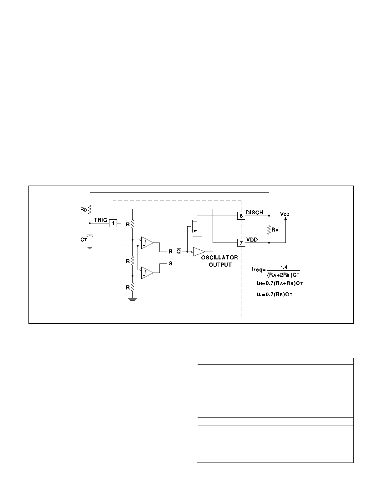
TRIG/DISCH: Oscillator control pins.TRIG is the oscillator timing input, which has an RC-type charge/discharge
signal controlling the chip’s internal oscillator. DISCH is
the pin which provides the low impedance discharge
path for the external RC network during normal operation. Oscillator frequency and maximum duty cycle are
computed as follows:
frequency ≈
duty cycle ≈
as shown in Figure 1.
For best performance, keep the lead from CT to GND as
short as possible.A separate ground connection for CT is
desirable.The minimum value of RA is 10kΩ, the minimum value of RB is 2.2kΩ, and the minimum value of CT
is 47pF.
VDD: The power input connection for this device. Total
VDD current is the sum of quiescent current and the
average OUT current. Knowing the operating frequency
and the MOSFET gate charge (Qg), average OUT current can be calculated from
IOUT = Qg ·F, where F is frequency.
To prevent noise problems, bypass VDD to GND with a
ceramic capacitor as close to the chip as possible in parallel with an electrolytic capacitor.
4
UCC1807-1/-2/-3
UCC2807-1/-2/-3
UCC3807-1/-2/-3
Figure 1.Oscillator Block Diagram
RA + RB
RA + 2RB
1.4
(RA + 2RB)CT
PIN DESCRIPTIONS (cont.)
APPLICATIONS INFORMATION
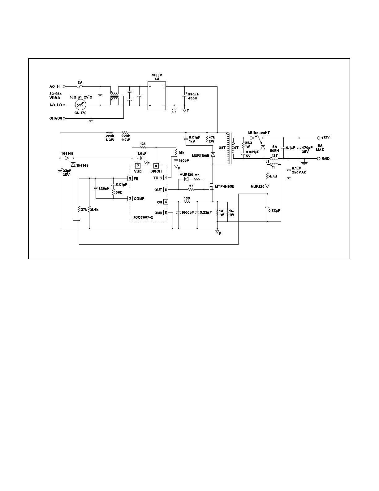
The circuit shown in Figure 2 illustrates the use of the
UCC3807 in a typical off-line application. The 100W,
200kHz, universal input forward converter produces a
regulated 12VDC at 8 Amps. The programmable maximum duty cycle of the UCC3807 allows operation down
to 80VRMS and up to 265VRMS with a simple RCD
clamp to limit the MOSFET voltage and provide core
reset. In this application the maximum duty cycle is set to
about 65%. Another feature of the design is the use of a
flyback winding on the output filter choke for both bootstrapping and voltage regulation. This method of loop
closure eliminates the optocoupler and secondary side
regulator, common to most off-line designs, while providing good line and load regulation.
T1:
Core: Magnetics Inc.#P-42625-UG (ungapped)
Primary: 28 turns of 2x #26AWG
Secondary: 6 turns of 50x0.2mm Litz wire
L1:
Core: Magnetics Inc.#P-42625-SG-37 (0.020” gap)
Main Winding: 13 turns of 2x #18AWG
Second Winding:11 turns of #26AWG
Magnetics Inc.
900 E.Butler Road
P.O.Box 391
Butler, PA 16003
Tel: (412) 282-8282
Fax:(412) 282-6955
UDG-95002-1
5
UNITRODE CORPORATION
7 CONTINENTAL BLVD. • MERRIMACK, NH 03054
TEL.(603) 424-2410 • FAX (603) 424-3460
Figure 2.Typical Off-line Application Using UCC3807-2
UDG-96174
UCC1807-1/-2/-3
UCC2807-1/-2/-3
UCC3807-1/-2/-3
APPLICATIONS INFORMATION (cont.)

IMPORTANT NOTICE
T exas Instruments and its subsidiaries (TI) reserve the right to make changes to their products or to discontinue
any product or service without notice, and advise customers to obtain the latest version of relevant information
to verify, before placing orders, that information being relied on is current and complete. All products are sold
subject to the terms and conditions of sale supplied at the time of order acknowledgement, including those
pertaining to warranty, patent infringement, and limitation of liability.
TI warrants performance of its semiconductor products to the specifications applicable at the time of sale in
accordance with TI’s standard warranty. Testing and other quality control techniques are utilized to the extent
TI deems necessary to support this warranty . Specific testing of all parameters of each device is not necessarily
performed, except those mandated by government requirements.
CERTAIN APPLICATIONS USING SEMICONDUCTOR PRODUCTS MAY INVOLVE POTENTIAL RISKS OF
DEATH, PERSONAL INJURY, OR SEVERE PROPERTY OR ENVIRONMENTAL DAMAGE (“CRITICAL
APPLICATIONS”). TI SEMICONDUCTOR PRODUCTS ARE NOT DESIGNED, AUTHORIZED, OR
WARRANTED TO BE SUITABLE FOR USE IN LIFE-SUPPORT DEVICES OR SYSTEMS OR OTHER
CRITICAL APPLICA TIONS. INCLUSION OF TI PRODUCTS IN SUCH APPLICATIONS IS UNDERST OOD TO
BE FULLY AT THE CUSTOMER’S RISK.
In order to minimize risks associated with the customer’s applications, adequate design and operating
safeguards must be provided by the customer to minimize inherent or procedural hazards.
TI assumes no liability for applications assistance or customer product design. TI does not warrant or represent
that any license, either express or implied, is granted under any patent right, copyright, mask work right, or other
intellectual property right of TI covering or relating to any combination, machine, or process in which such
semiconductor products or services might be or are used. TI’s publication of information regarding any third
party’s products or services does not constitute TI’s approval, warranty or endorsement thereof.
Copyright 1999, Texas Instruments Incorporated
 Loading...