

Page 1

ADVANCE INFORMATION
User's Guide
SLUUBS3A–October 2017–Revised January 2018
UCC28056EVM-296 Evaluation Module
This user’s guide provides basic evaluation instruction from a viewpoint of system operation of a standalone PFC boost power converter.
Contents
1 Introduction ................................................................................................................... 4
2 Description.................................................................................................................... 4
3 Performance Specifications ................................................................................................ 5
4 Test Setup .................................................................................................................... 5
5 Test Points.................................................................................................................... 7
6 Terminals ..................................................................................................................... 7
7 Test Procedure............................................................................................................... 7
8 Performance Data and Typical Characteristic Curves.................................................................. 9
9 Schematic, Assembly Drawing and Bill of Materials................................................................... 18
List of Figures
1 UCC28056EVM-296 Recommended Test Setup........................................................................ 6
2 Efficiency...................................................................................................................... 9
3 Load Regulation vs Output Power....................................................................................... 10
4 Line Regulation vs Input Voltage......................................................................................... 10
5 Power Factor vs Output Power........................................................................................... 11
6 THD vs Output Power ..................................................................................................... 11
7 85 VAC Startup No Load.................................................................................................. 11
8 85 VAC Startup Full Load................................................................................................. 11
9 115 VAC Startup No Load ................................................................................................ 11
10 115 VAC Startup Full Load ............................................................................................... 11
11 230 VAC Startup No Load ................................................................................................ 11
12 230 VAC Startup Full Load ............................................................................................... 11
13 265 VAC Startup No Load ................................................................................................ 12
14 265 VAC Startup Full Load ............................................................................................... 12
15 Low-Line Voltage and Current............................................................................................ 13
16 High-Line Voltage and Current........................................................................................... 14
17 85 VAC Valley Switching 50-mA Load .................................................................................. 14
18 115 VAC Valley Switching 50-mA Load................................................................................. 15
19 230 VAC Valley Switching 100-mA Load ............................................................................... 15
20 265 VAC Valley Switching 100-mA Load .............................................................................. 16
21 Q1 Max Vds Stress ........................................................................................................ 16
22 D4 Max Voltage Stress.................................................................................................... 17
23 UCC28056EVM-296 Schematic.......................................................................................... 18
24 UCC28056EVM-296 Top Assembly Drawing (Top view)............................................................. 19
25 UCC28056EVM-296 Bottom Layer Assembly Drawing (Top view).................................................. 19
26 UCC28056EVM-296 Top Copper Assembly Drawing (Top view) ................................................... 20
SLUUBS3A–October 2017–Revised January 2018
Submit Documentation Feedback
Copyright © 2017–2018, Texas Instruments Incorporated
UCC28056EVM-296 Evaluation Module
1
Page 2

27 UCC28056EVM-296 Bottom Copper Assembly Drawing (Top view)................................................ 20
1 EVM Performance Specification ........................................................................................... 5
2 Test Points.................................................................................................................... 7
3 List of Terminals ............................................................................................................. 7
4 Total Standby Power ........................................................................................................ 9
5 Bill of Materials ............................................................................................................. 21
Trademarks
All trademarks are the property of their respective owners.
ADVANCE INFORMATION
www.ti.com
List of Tables
2
UCC28056EVM-296 Evaluation Module
SLUUBS3A–October 2017–Revised January 2018
Copyright © 2017–2018, Texas Instruments Incorporated
Submit Documentation Feedback
Page 3

WARNING
ADVANCE INFORMATION
www.ti.com
General Texas Instruments High Voltage Evaluation (TI HV EVM) User Safety Guidelines
Always follow TI’s setup and application instructions, including use of all interface components within their
recommended electrical rated voltage and power limits. Always use electrical safety precautions to help
ensure your personal safety and those working around you. Contact TI's Product Information Center
http://support/ti./com for further information.
Save all warnings and instructions for future reference.
Failure to follow warnings and instructions may result in personal injury, property damage, or
death due to electrical shock and burn hazards.
The term TI HV EVM refers to an electronic device typically provided as an open framed, unenclosed
printed circuit board assembly. It is intended strictly for use in development laboratory environments,
solely for qualified professional users having training, expertise and knowledge of electrical safety
risks in development and application of high voltage electrical circuits. Any other use and/or
application are strictly prohibited by Texas Instruments. If you are not suitable qualified, you should
immediately stop from further use of the HV EVM.
1. Work Area Safety
1. Keep work area clean and orderly.
2. Qualified observer(s) must be present anytime circuits are energized.
3. Effective barriers and signage must be present in the area where the TI HV EVM and its interface
electronics are energized, indicating operation of accessible high voltages may be present, for the
purpose of protecting inadvertent access.
4. All interface circuits, power supplies, evaluation modules, instruments, meters, scopes and other
related apparatus used in a development environment exceeding 50Vrms/75VDC must be
electrically located within a protected Emergency Power Off EPO protected power strip.
5. Use stable and nonconductive work surface.
6. Use adequately insulated clamps and wires to attach measurement probes and instruments. No
freehand testing whenever possible.
2. Electrical Safety
As a precautionary measure, it is always a good engineering practice to assume that the entire EVM
may have fully accessible and active high voltages.
1. De-energize the TI HV EVM and all its inputs, outputs and electrical loads before performing any
electrical or other diagnostic measurements. Revalidate that TI HV EVM power has been safely
de-energized.
2. With the EVM confirmed de-energized, proceed with required electrical circuit configurations,
wiring, measurement equipment connection, and other application needs, while still assuming the
EVM circuit and measuring instruments are electrically live.
3. After EVM readiness is complete, energize the EVM as intended.
WARNING: WHILE THE EVM IS ENERGIZED, NEVER TOUCH THE EVM OR ITS ELECTRICAL
CIRCUITS AS THEY COULD BE AT HIGH VOLTAGES CAPABLE OF CAUSING ELECTRICAL
SHOCK HAZARD.
3. Personal Safety
1. Wear personal protective equipment (for example, latex gloves or safety glasses with side shields)
or protect EVM in an adequate lucent plastic box with interlocks to protect from accidental touch.
Limitation for safe use:
EVMs are not to be used as all or part of a production unit.
SLUUBS3A–October 2017–Revised January 2018
Submit Documentation Feedback
Copyright © 2017–2018, Texas Instruments Incorporated
UCC28056EVM-296 Evaluation Module
3
Page 4

ADVANCE INFORMATION
Introduction
1 Introduction
The purpose of the UCC28056EVM-296 (EVM) is to aid in evaluation of the UCC28056 transition mode
boost PFC converter. The EVM is a stand-alone PFC converter designed to operate with 85 to 265 V
47 to 63 Hz, AC input and up to 165-W DC output from 90 VAC to 265 VAC and 140 W at 85 VAC. The
EVM can be used as it is delivered without additional work, to evaluate a transition mode boost PFC
converter. This user’s guide provides basic evaluation instruction from a viewpoint of system operation of
a stand-alone PFC boost power converter.
2 Description
2.1 Typical Applications
This EVM is used in the following applications:
• AC adapter front end
• Set top box
• Desktop computing
• Gaming
• Electronic lamp ballast
• Digital TV
• Entry-level server and web server
www.ti.com
RMS
,
2.2 Features
This EVM has the following features:
• Unified algorithm for working in critical mode (CRM) and discontinuous conduction mode (DCM) with a
high power factor across the entire operating range
• AC input voltage from 85 to 265 V
• AC line frequency from 47 to 63 Hz
• Up to 165-W output power
• High efficiency
• TM, DCM control gives improved light-load efficiency
• Burst mode for reduced standby consumption
• Non-linear gain gives improved transient response
• User-adjustable valley switching
• Robust full-featured protection including overtemperature protection, brown-out protection, output
overvoltage, cycle-by-cycle overcurrent, and gross overcurrent protections
• Test points to facilitate device and topology evaluation
RMS
4
UCC28056EVM-296 Evaluation Module
SLUUBS3A–October 2017–Revised January 2018
Copyright © 2017–2018, Texas Instruments Incorporated
Submit Documentation Feedback
Page 5
ADVANCE INFORMATION
www.ti.com
3 Performance Specifications
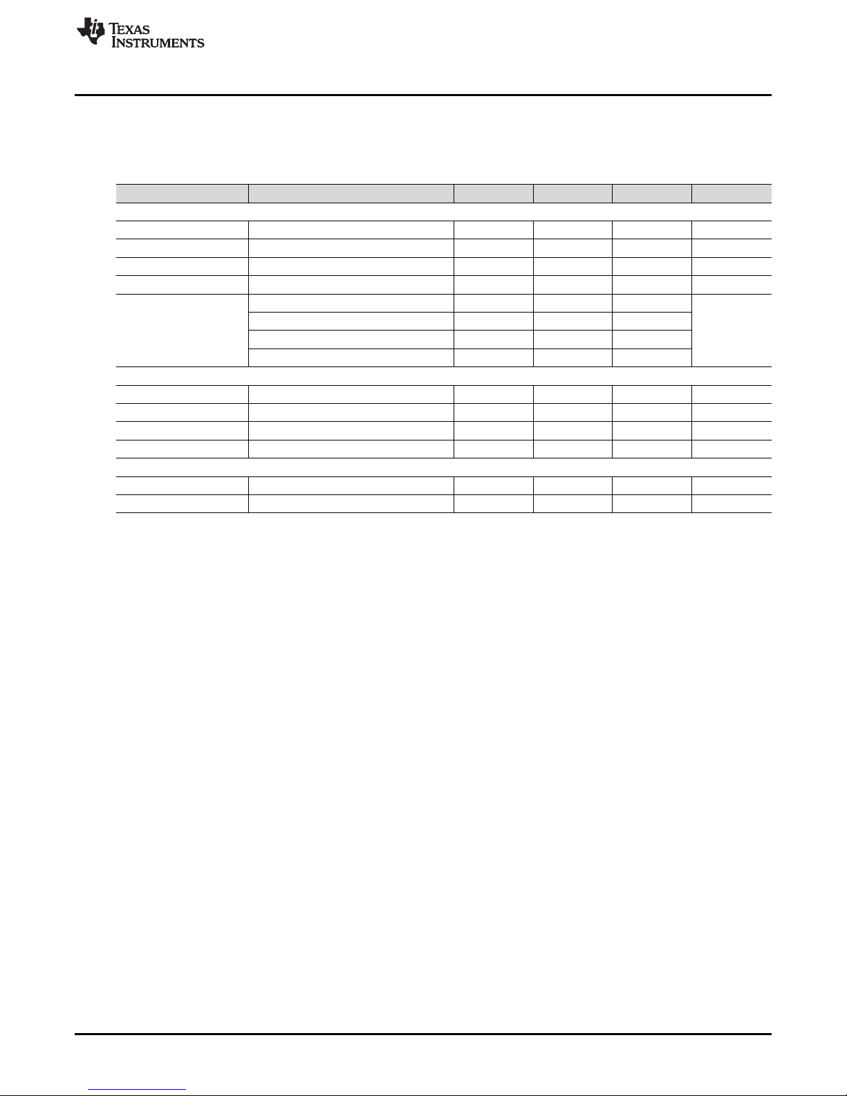
Table 1 displays the EVM performance specifications.
Parameter Test Conditions MIN TYP MAX Units
Input Characteristics
AC Voltage Range 85 265 V
AC Voltage Frequency 47 63 Hz
VCC UVLO On 10.65 VDC
VCC UVLO Off 8.85 VDC
Input = 85 VAC, Full Load = 165 W 1.85
Input DC Current
Output Characteristics
Output Voltage No Load to Full Load 390 VDC
Output Power 90 to 265 VAC 165 W
Output Power 85 VAC 140 W
Output Voltage Ripple 10 Vpp
System Characteristics
Peak Efficiency 97 %
Operating Temperature Natural Convection 25 °C
Input = 115 VAC, Full Load = 165 W 1.43
Input = 230 VAC, Full Load = 165 W 0.71
Input = 265 VAC, Full Load = 165 W 0.64
Performance Specifications
Table 1. EVM Performance Specification
RMS
Arms
4 Test Setup
4.1 Test Equipment
DC Voltage Source: External DC input for VCC. The DC source should be capable of supplying 12 V and
up to 100 mA.
AC Voltage Source: Capable of single-phase output AC voltage 85 to 265 VAC, 47 to 63 Hz, adjustable,
with minimum power rating 200 W and current limit function. The AC voltage source to be used should
meet IEC60950 reinforced insulation requirement.
DC Digital Multimeter: One unit capable of 0 to 450 VDC input range, four-digit display preferred.
Output Load: DC load capable of receiving 380 to 410 VDC, 0.5 A, and 0 to 200 W or greater, with the
capability to display load current, load power, and so forth.
Digital AC Power Meter: Capable of 0 to 300 VAC voltage measurement, 0 to 10 Arms current
measurement. Native power factor measurement and input current THD measurement is preferred.
Oscilloscope: Capable of 500-MHz full bandwidth, digital or analog: if digital, 5 Gsps, or better.
Fan: 200 to 400 LFM forced air cooling is recommended, but not required.
Recommended Wire Gauge: Capable of 10 A, or better than #14 AWG, with the total length of wire less
than 8 feet (4 feet input and 4 feet return).
SLUUBS3A–October 2017–Revised January 2018
Submit Documentation Feedback
Copyright © 2017–2018, Texas Instruments Incorporated
UCC28056EVM-296 Evaluation Module
5
Page 6
ADVANCE INFORMATION
Test Setup
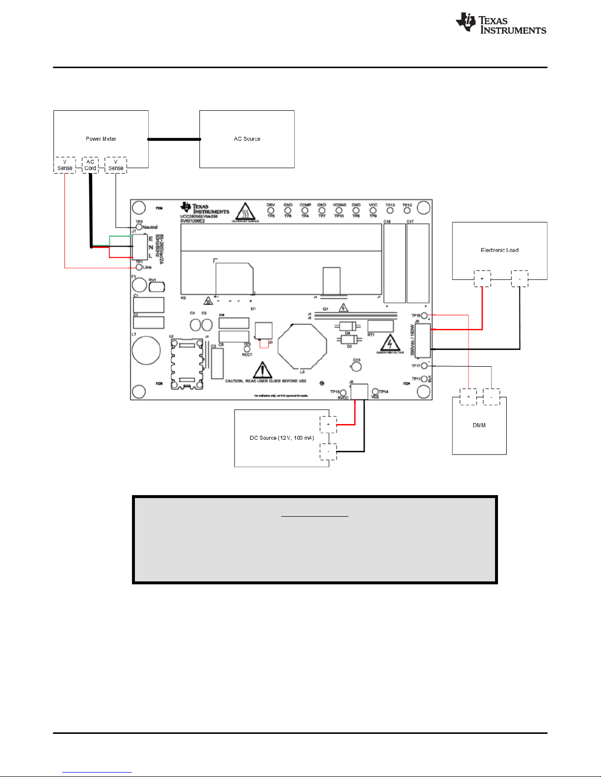
4.2 Recommended Test Setup
Figure 1 illustrates the recommended test setup.
www.ti.com
Figure 1. UCC28056EVM-296 Recommended Test Setup
High voltages that may cause injury exist on this evaluation
module (EVM). Please ensure all safety procedures are followed
when working on this EVM. Never leave a powered EVM
unattended.
6
UCC28056EVM-296 Evaluation Module
WARNING
SLUUBS3A–October 2017–Revised January 2018
Copyright © 2017–2018, Texas Instruments Incorporated
Submit Documentation Feedback
Page 7
ADVANCE INFORMATION
www.ti.com
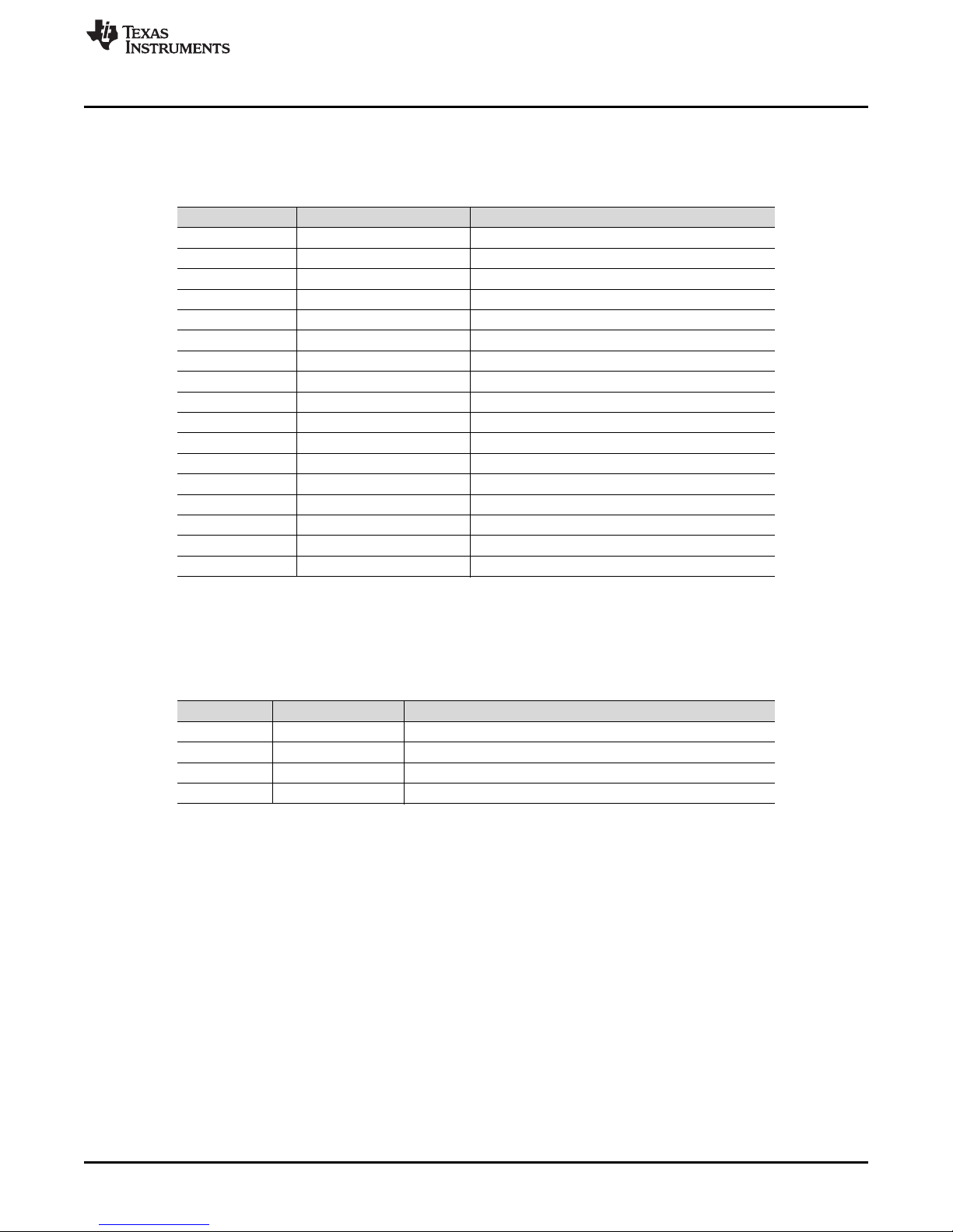
5 Test Points
Table 2 lists the EVM test points.
Test Points Name Description
Test Points
Table 2. Test Points
TP1 Line AC line
TP2 Neutral AC neutral
TP3 Rect AC rectifier output
TP4 COMP Transconductance amplifier output
TP5 DRV Gate-drive output
TP6 GND Ground
TP7 GND Ground
TP8 GND Ground
TP9 VCC VCCsense
TP10 VOSNS Voltage error amplifier inverting input
TP11 BLK Bulk sense
TP12 TP12 Small signal injection terminal
TP13 TP13 Small signal injection terminal
TP14 VEE DC input ground
TP15 RVCC Positive DC input
TP16 VOUT+ Output voltage
TP17 VOUT– Output voltage return
6 Terminals
Table 3 lists the EVM terminals.
Terminal Name Description
J1 AC Input 3-pin, AC power input, 85 V–265 V
J3 I_IND Inductor current sense
J8 RVCC 2-pin, DC power input, 12 V typical
J9 VOUT 4-pin, output voltage terminal, 390 V typical
7 Test Procedure
Use the following steps for the test procedure:
1. Refer to Figure 1 for basic setup. The required equipment for this measurement is listed in Table 2.
2. Before making electrical connections, visually check the board to make sure there are no suspected
spots of damage.
3. Use a loop of wire to short the J3 terminals. Connect a current probe around the wire loop to measure
the inductor current using an oscilloscope.
4. Keep the AC voltage source output off. Connect the AC source to the input of the AC power meter.
Connect the output of the AC power meter to J1 with AC_line to J1-3, AC_earth to J1-1, AC_neutral to
J1-2. Isolate the AC voltage source and meet the IEC60950 requirement. Set the AC output voltage
and frequency within the range specified in Table 1, between 85 and 265 VAC and 47 to 63 Hz. Set
the AC source current limit to 8.5 A.
Table 3. List of Terminals
SLUUBS3A–October 2017–Revised January 2018
Submit Documentation Feedback
Copyright © 2017–2018, Texas Instruments Incorporated
UCC28056EVM-296 Evaluation Module
7
Page 8

ADVANCE INFORMATION
Test Procedure
While the EVM does have a fuse installed, failure to set an appropriate current
limit may result in damage to the fuse or other EVM components.
5. Keep the DC voltage source output off. Connect the DC source to J2. Set the DC output voltage to
12 V and the current limit to 100 mA.
6. Connect an electronic load set to either constant-current mode or constant-resistance mode. The load
range is from 0 to 423 mA.
7. If the load does not have a current or a power display, TI recommends inserting a current meter
between the output voltage and the electronic load.
8. Connect a voltage meter to TP16 and TP17 to monitor the output voltage
9. Turn on the AC voltage source output.
10. Turn on the DC source output.
7.1 Equipment Shutdown
Shut down the equipment using the following steps:
1. Shut down the AC voltage source.
2. Shut down the DC voltage source.
3. Shut down the electronic load.
www.ti.com
CAUTION
WARNING
High voltage may still be present after turning off the AC and DC
sources. Use the electronic load to discharge the output
capacitance before handling the EVM.
8
UCC28056EVM-296 Evaluation Module
SLUUBS3A–October 2017–Revised January 2018
Copyright © 2017–2018, Texas Instruments Incorporated
Submit Documentation Feedback
Page 9
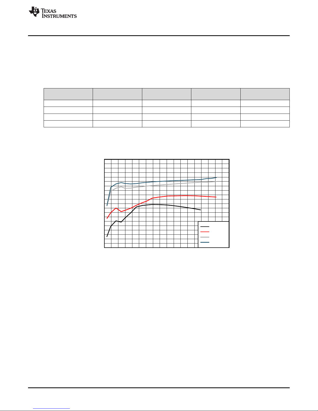
Output Power (W)
Efficiency (%)
0 20 40 60 80 100 120 140 160 180
0.9
0.91
0.92
0.93
0.94
0.95
0.96
0.97
0.98
0.99
1
d000
85Vac
115Vac
230Vac
265Vac
ADVANCE INFORMATION
www.ti.com
Performance Data and Typical Characteristic Curves
8 Performance Data and Typical Characteristic Curves
8.1 Standby Power
Table 4 lists the total standby power measurement. The electronic load is physically disconnected from J9
for this test. The average input power is measured at VIand external VCCover a 5 minute interval.
Table 4. Total Standby Power
Input Voltage (V
85 23 12.00743 104.0338 24.249
115 24 12.01006 107.022 25.285
230 39 12.00832 105.630 40.268
265 45 12.00830 105.902 46.272
) Input Power (mW) VCC Voltage (V) VCC Current (µA)
RMS
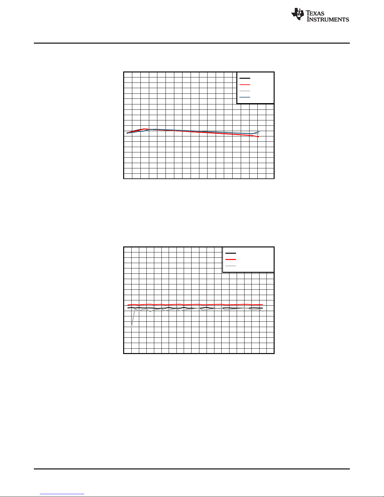
8.2 Efficiency
Figure 2 illustrates the EVM efficiency graph.
Total Standby Power
(mW)
SLUUBS3A–October 2017–Revised January 2018
Submit Documentation Feedback
Figure 2. Efficiency
Copyright © 2017–2018, Texas Instruments Incorporated
UCC28056EVM-296 Evaluation Module
9
Page 10
Line Voltage (Vrms)
Output Voltage (V)
80 100 120 140 160 180 200 220 240 260 280
380
382
384
386
388
390
392
394
396
398
400
d000
Iout = 0mA
Iout = 120mA
Iout = 420mA
Output Power (W)
Output Voltage (V)
0 20 40 60 80 100 120 140 160 180
380
382
384
386
388
390
392
394
396
398
400
d000
85Vac
115Vac
230Vac
265Vac
ADVANCE INFORMATION
Performance Data and Typical Characteristic Curves
8.3 Load Regulation
Figure 3 illustrates the load regulation versus output power graph.
Figure 3. Load Regulation vs Output Power
www.ti.com
8.4 Line Regulation
Figure 4 illustrates the line regulation versus input voltage graph.
Figure 4. Line Regulation vs Input Voltage
10
UCC28056EVM-296 Evaluation Module
Copyright © 2017–2018, Texas Instruments Incorporated
SLUUBS3A–October 2017–Revised January 2018
Submit Documentation Feedback
Page 11

Output Power (W)
THD (%)
40 60 80 100 120 140 160 180
8%
10%
12%
14%
16%
18%
20%
d000
85Vac
115Vac
230Vac
265Vac
Output Power (W)
Power Factor (%)
0 20 40 60 80 100 120 140 160 180
0.4
0.45
0.5
0.55
0.6
0.65
0.7
0.75
0.8
0.85
0.9
0.95
1
d000
85Vac
115Vac
230Vac
265Vac
ADVANCE INFORMATION
www.ti.com
8.5 Power Factor
Figure 5 illustrates the power factor versus output power graph.
Performance Data and Typical Characteristic Curves
Figure 5. Power Factor vs Output Power
8.6 THD
Figure 6 illustrates the THD versus output power graph.
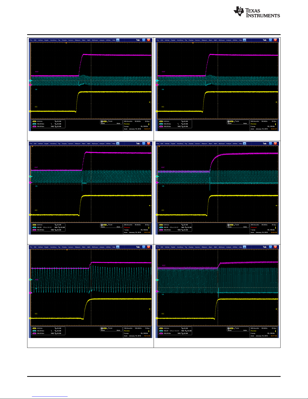
8.7 Startup
The following waveforms show the output voltage behavior when the line voltage has already been
applied and the instant the VCC voltage exceeds the startup threshold. From Figure 7 to Figure 14,
Channel 1 = VCC, Channel 2 = Input Voltage and Channel 3 = Output Voltage
SLUUBS3A–October 2017–Revised January 2018
Submit Documentation Feedback
Copyright © 2017–2018, Texas Instruments Incorporated
Figure 6. THD vs Output Power
UCC28056EVM-296 Evaluation Module
11
Page 12
ADVANCE INFORMATION
Performance Data and Typical Characteristic Curves
Figure 7. 85 VAC Startup No Load Figure 8. 85 VAC Startup Full Load
www.ti.com
Figure 9. 115 VAC Startup No Load Figure 10. 115 VAC Startup Full Load
Figure 11. 230 VAC Startup No Load Figure 12. 230 VAC Startup Full Load
12
UCC28056EVM-296 Evaluation Module
SLUUBS3A–October 2017–Revised January 2018
Copyright © 2017–2018, Texas Instruments Incorporated
Submit Documentation Feedback
Page 13
ADVANCE INFORMATION
www.ti.com
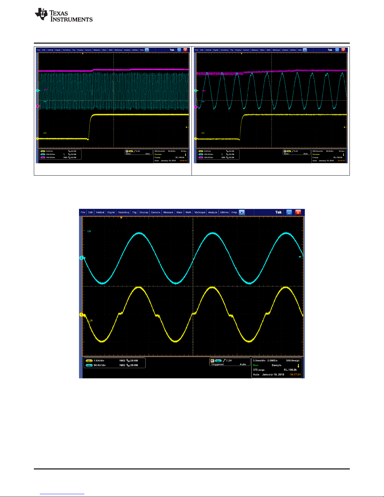
Figure 13. 265 VAC Startup No Load Figure 14. 265 VAC Startup Full Load
8.8 Line Voltage and Line Current
Figure 15 and Figure 16 illustrate the low- and high-line voltage and current waveforms.
Performance Data and Typical Characteristic Curves
SLUUBS3A–October 2017–Revised January 2018
Submit Documentation Feedback
Figure 15. Low-Line Voltage and Current
UCC28056EVM-296 Evaluation Module
Copyright © 2017–2018, Texas Instruments Incorporated
13
Page 14

ADVANCE INFORMATION
Performance Data and Typical Characteristic Curves
www.ti.com
8.9 Valley Switching
The following waveforms shows drain to source voltage of the MOSFET and the valley switching action on
the EVM.
Figure 16. High-Line Voltage and Current
Figure 17. 85 VAC Valley Switching 50-mA Load
14
UCC28056EVM-296 Evaluation Module
SLUUBS3A–October 2017–Revised January 2018
Copyright © 2017–2018, Texas Instruments Incorporated
Submit Documentation Feedback
Page 15

ADVANCE INFORMATION
www.ti.com
Performance Data and Typical Characteristic Curves
Figure 18. 115 VAC Valley Switching 50-mA Load
Figure 19. 230 VAC Valley Switching 100-mA Load
SLUUBS3A–October 2017–Revised January 2018
Submit Documentation Feedback
Copyright © 2017–2018, Texas Instruments Incorporated
UCC28056EVM-296 Evaluation Module
15
Page 16

ADVANCE INFORMATION
Performance Data and Typical Characteristic Curves
www.ti.com
8.10 Voltage Stress Q1
Figure 21 illustrates the voltage stress Q1 waveform.
Figure 20. 265 VAC Valley Switching 100-mA Load
16
UCC28056EVM-296 Evaluation Module
Figure 21. Q1 Max Vds Stress
SLUUBS3A–October 2017–Revised January 2018
Copyright © 2017–2018, Texas Instruments Incorporated
Submit Documentation Feedback
Page 17

ADVANCE INFORMATION
www.ti.com
8.11 Voltage Stress D4
Figure 22 illustrates the voltage stress D4 waveform.
Performance Data and Typical Characteristic Curves
Figure 22. D4 Max Voltage Stress
SLUUBS3A–October 2017–Revised January 2018
Submit Documentation Feedback
Copyright © 2017–2018, Texas Instruments Incorporated
UCC28056EVM-296 Evaluation Module
17
Page 18

600V
~
3
+
1
~
2
-
4
D1
VOSNS
Line
Neutral
GATE
30V
D3
DRAIN
453k
R11
0.13R90.13
R10
VCC
RV1
600V
D4
100V
D5
3.24M
R15
3.24M
R16
3.24M
R17
2 11
NC
4
NC
6
NC
8
240
µH
750317130
L3
68µF
C17
68µF
C16
6
7
1
12
20mH
L2
744825320
1000pF
C5
1000pF
C4
0.47µF
C6
220µH
L1
3.24M
R5
3.24M
R6
3.24M
R7
10.0
R22
10µF
C15
10pF
C13
0.22µF
C3
F1
37215000001
2200pF
C14
J3
J2
J5
J4
J7
TP3
TP16
TP17
TP6
OUTPUT: 390VDC NOMINAL, 0.423A M AX
1
2
J8
2
1
3
Q1
STF28N60DM2
51
R14
TP15
TP12
TP13
1
2
3
J1
TP5
TP10
TP4
DRV
GND
ZCD
COMP
1
2
3
4
J9
0.47µF
C12
10
R3
1.0
R2
TP1
TP2
PE
TP14
SOURCE
NOTES:
LINE INPUTVOLTAGE: 85VRMS - 265VRMS,
47Hz- 63Hz
OUTPUT VOLTAGE: 390VDC nominal
MAXIMUMOUTPUT POWER: 165W
VOUT+
DRV
5
COMP
6
GND
4
VOSNS
1
ZCD/CS
2
VCC
3
U1
UCC28056DBV
3.0k
R12
36.5k
R18
120k
R19
75k
R20
390k
R21
TP11
TP7 TP8
3300pF
C10
0
R13
0.033µF
C7
1µF
C8
180k
R1
J6
TP9
10pF
C9
82.5k
R4
24.3k
R8
600V
D2
RTN
VOUT-
VEE
GND
0.47µF
C18
0.33µFC10.33µF
C2
470pF
C11
4.70ohm
t°
RT1
Copyright © 2018, Texas Instruments Incorporated
Schematic, Assembly Drawing and Bill of Materials
www.ti.com
18
SLUUBS3A– October 2017–Revised January 2018
Submit Documentation Feedback
Copyright © 2017–2018, Texas Instruments Incorporated
UCC28056EVM-296 Evaluation Module
ADVANCE INFORMATION
9 Schematic, Assembly Drawing and Bill of Materials
9.1 Schematic
Figure 23 illustrates the EVM schematic.
Figure 23. UCC28056EVM-296 Schematic
Page 19

ADVANCE INFORMATION
www.ti.com
9.2 Assembly Drawing
Figure 24 through Figure 27 illustrate the EVM assembly drawings.
Schematic, Assembly Drawing and Bill of Materials
Figure 24. UCC28056EVM-296 Top Assembly Drawing (Top view)
Figure 25. UCC28056EVM-296 Bottom Layer Assembly Drawing (Top view)
SLUUBS3A–October 2017–Revised January 2018
Submit Documentation Feedback
Copyright © 2017–2018, Texas Instruments Incorporated
UCC28056EVM-296 Evaluation Module
19
Page 20

ADVANCE INFORMATION
Schematic, Assembly Drawing and Bill of Materials
www.ti.com
Figure 26. UCC28056EVM-296 Top Copper Assembly Drawing (Top view)
Figure 27. UCC28056EVM-296 Bottom Copper Assembly Drawing (Top view)
20
UCC28056EVM-296 Evaluation Module
SLUUBS3A–October 2017–Revised January 2018
Copyright © 2017–2018, Texas Instruments Incorporated
Submit Documentation Feedback
Page 21

ADVANCE INFORMATION
www.ti.com
9.3 Bill of Materials
Table 5 contains the EVM BOM.
Designator QTY Value Description Package Reference Part Number
PCB1 1 Printed Circuit Board SV601296
C1, C2 1 0.33uF CAP, Film, 0.33 µF, 630 V, ±20%, TH B32922_17.5mm BFC233841334
C3 2 0.22uF CAP, Film, 0.22 µF, 630 V, ±10%, TH B32922_12.5mm B32922C3224K
C4, C5 2 1000pF CAP, CERM, 1000 pF, V, ±20%, E, D7xT6mm D7xT6mm CD45-E2GA102M-NKA
C6 1 0.47uF CAP, Film, 0.47 µF, 450 V, ±5%, TH 18x6.5mm 450MPK474J
C7 1 0.033uF CAP, CERM, 0.033 µF, 50 V, ±5%, X7R, 0603 0603 06035C333JAT2A
C8 1 1uF CAP, CERM, 1 µF, 25 V, ±10%, X7R, 0603 0603 06033C105KAT2A
C9 1 10pF CAP, CERM, 10 pF, 1000 V, ±5%, C0G/NP0, 0805 0805 VJ0805A100JXGAT5Z
C10 1 3300pF CAP, CERM, 3300 pF, 100 V, ±5%, X7R, 0603 0603 06031C332JAT2A
C11 1 470pF CAP, CERM, 470 pF, 100 V, ±10%, X7R, 0603 0603 06031C471KAT2A
C12 1 0.47uF CAP, CERM, 0.47 µF, 50 V, ±10%, X7R, 0805 0805 GRM21BR71H474KA88L
C13 1 10pF CAP, CERM, 10 pF, 10 V, ±10%, X7R, 0603 0603 0603ZC100KAT2A
C14 1 2200pF CAP, CERM, 2200 pF, 50 V, ±5%, C0G/NP0, 1206 1206 GRM3195C1H222JA01D
C15 1 10uF CAP, AL, 10 µF, 50 V, ±20%, TH D5xL11mm EKMG500ELL100ME11D
C16, C17 2 68uF CAP, AL, 68 µF, 450 V, ±20%, TH D12.5xL45mm 450BXW68MEFC12.5X45
D1 1 600V Diode, P-N-Bridge, 600 V, 4 A, TH GBU GBU4J-BP
D2 1 600V Diode, Fast Rectifier, 600 V, 3 A, TH DO-201AD MR856G
D3 1 30V Diode,Schottky, 30 V, 0.35 A, SOD-323 SOD-323 BAT48JFILM
D4 1 600V Diode, Ultrafast, 600 V, 5 A, TH DO-201AD STTH5L06
D5 1 100V Diode, Switching, 100 V, 0.15 A, SOD-123FL SOD-123FL 1N4148WFL-G3-08
F1 1 Fuse, 5 A, 250VAC/VDC, TH TR5 fuse 8.5mm DIA 37215000001
H1, H4, H6, H8 4 HEX STANDOFF 6-32 NYLON 1-1/2" HEX STANDOFF 6-32
H2, H5, H7, H9 4 Standoff, Hex, 0.5"L #6-32 Nylon 6-32 HEX Nylon standoff
H3 1 Custom HeatSink, 120x42x10mm HeatSink, 120x42x10mm FL12-013-120x42
H10, H11, H12 3 MACHINE SCREW PAN PHILLIPS, 5/16", 4-40 PMSSS 440 0031 PH
H13, H14, H15 3 Washer, Split Lock, #4 4693
H16 1 TO-220 Mounting Kit TO-220 Mounting Kit 4880SG
H17, H18, H19 3 Nut, Hex, 1/4" Thick, #4-40 HNSS440
J1 1 Terminal Block, 5.08 mm, 3x1, Brass, TH 3x1 5.08 mm Terminal
J2, J4 2 Jumper Wire, 700mil spacing, Violet, pkg of 150, TH 700 mil Jumper Wire 923345-07-C
J3 1 Terminal Block, 5.08 mm, 2x1, TH 2POS Terminal Block 1715721
J5, J6 2 Jumper Wire, 2" spacing, Red, pkg of 100, TH Jumper Wire, 2" Spacing,
J7 1 Jumper Wire, 500mil spacing, Green, pkg of 200 500 mil Jumper Wire 923345-05-C
J8 1 Terminal Block, 5.08 mm, 2x1, Brass, TH 2x1 5.08 mm Terminal
J9 1 Terminal Block, 5.08 mm, 4x1, Brass, TH 4x1 5.08 mm Terminal
L1 1 220uH Inductor, Wirewound, Ferrite, 220 µH, 2.42 A, 0.168 ohm,THD630xH810mil DC630R-224K
Schematic, Assembly Drawing and Bill of Materials
Table 5. Bill of Materials
NYLON 1-1/2 inch
0.500 mil
Block
Red, Pkg of 100
Block
Block
4824
1903C
ED120/3DS
923345-20-C
ED120/2DS
ED120/4DS
L2 1 20mH Coupled inductor, 20 mH, 3 A, 0.16 ohm, TH 30x35x21mm 744825320
L3 1 200uH Inductor, 200 µH, 0.235 ohm, TH TH, 5-Leads, Body
LBL1 1 Thermal Transfer Printable Labels, 0.650" W x 0.200" H -
Q1 1 600V MOSFET, N-CH, 600 V, 21 A, TO-220FP TO-220FP STF28N60DM2
R1 1 180k RES, 180 k, 5%, 0.1 W, 0603 0603 CRCW0603180KJNEA
R2 1 1.0 RES, 1.0, 5%, 0.125 W, 0805 0805 CRCW08051R00JNEA
R3 1 10 RES, 10, 5%, 0.125 W, 0805 0805 CRCW080510R0JNEA
R4 1 82.5k RES, 82.5 k, 1%, 0.125 W, 0805 0805 ERJ-6ENF8252V
R5, R6, R7, R15,
R16, R17
R8 1 24.3k RES, 24.3 k, 1%, 0.1 W, 0603 0603 CRCW060324K3FKEA
R9, R10 2 0.13 RES, 0.13, 1%, 0.5 W, 1206 1206 CSR1206FTR130
6 3.24Meg RES, 3.24 M, 1%, 0.25 W, 1206 1206 CRCW12063M24FKEA
SLUUBS3A–October 2017–Revised January 2018
Submit Documentation Feedback
26.16x26.16mm
10,000 per roll
PCB Label 0.650"H x
0.200"W
Copyright © 2017–2018, Texas Instruments Incorporated
750316570
THT-14-423-10
UCC28056EVM-296 Evaluation Module
21
Page 22
ADVANCE INFORMATION
Revision History
Table 5. Bill of Materials (continued)
Designator QTY Value Description Package Reference Part Number
R11 1 453k RES, 453 k, 1%, 0.25 W, 1206 1206 CRCW1206453KFKEA
R12 1 3.0k RES, 3.0 k, 5%, 0.1 W, 0603 0603 CRCW06033K00JNEA
R13 1 0 RES, 0, 5%, 0.25 W, 1206 1206 CRCW12060000Z0EA
R14 1 51 RES, 51, 5%, 0.25 W, 1206 1206 CRCW120651R0JNEA
R18 1 36.5k RES, 36.5 k, 1%, 0.25 W, 1206 1206 CRCW120636K5FKEA
R19 1 120k RES, 120 k, 5%, 0.25 W, 1206 1206 CRCW1206120KJNEA
R20 1 75k RES, 75 k, 5%, 0.25 W, 1206 1206 CRCW120675K0JNEA
R21 1 390k RES, 390 k, 5%, 0.25 W, 1206 1206 CRCW1206390KJNEA
R22 1 10.0 RES, 10.0, 1%, 0.25 W, 1206 1206 CRCW120610R0FKEA
RT1 1 4.70 ohm Thermistor NTC, 4.70 ohm, 20%, 8.5mm Disc 8.5mm Disc B57153S0479M000
RV1 1 VARISTOR 490V 1.2KA DISC 7MM Dia. 7mm V300LA2P
SIL1 1 Silcon Thermal Pad 24x21 mm SP900S-0.009-00-114
TP1, TP3, TP9,
TP12, TP15, TP16
TP2, TP4, TP5,
TP10, TP11
TP6, TP7, TP8,
TP13, TP14, TP17
U1 1 6-Pin Single-Phase Transition-Mode PFC Controller,
6 Test Point, Multipurpose, Red, TH Red Multipurpose Testpoint 5010
5 Test Point, Multipurpose, White, TH White Multipurpose
6 Test Point, Multipurpose, Black, TH BlackMultipurpose
DBV0006A (SOT-23-6)
Testpoint
Testpoint
DBV0006A UCC28056DBV
Revision History
NOTE: Page numbers for previous revisions may differ from page numbers in the current version.
www.ti.com
5012
5011
Changes from Original (October 2017) to A Revision .................................................................................................... Page
• Updated graphs and waveforms in Section 8.......................................................................................... 9
• Added Standby Power section........................................................................................................... 9
• Added Startup section................................................................................................................... 11
• Added Valley Switching section........................................................................................................ 14
• Moved C2 in the bill of materials....................................................................................................... 21
• Changed the Q1 part number in the bill of materials................................................................................ 21
• Changed parameters on RT1 in the bill of materials................................................................................ 21
22
Revision History
SLUUBS3A–October 2017–Revised January 2018
Copyright © 2017–2018, Texas Instruments Incorporated
Submit Documentation Feedback
Page 23

STANDARD TERMS FOR EVALUATION MODULES
1. Delivery: TI delivers TI evaluation boards, kits, or modules, including any accompanying demonstration software, components, and/or
documentation which may be provided together or separately (collectively, an “EVM” or “EVMs”) to the User (“User”) in accordance
with the terms set forth herein. User's acceptance of the EVM is expressly subject to the following terms.
1.1 EVMs are intended solely for product or software developers for use in a research and development setting to facilitate feasibility
evaluation, experimentation, or scientific analysis of TI semiconductors products. EVMs have no direct function and are not
finished products. EVMs shall not be directly or indirectly assembled as a part or subassembly in any finished product. For
clarification, any software or software tools provided with the EVM (“Software”) shall not be subject to the terms and conditions
set forth herein but rather shall be subject to the applicable terms that accompany such Software
1.2 EVMs are not intended for consumer or household use. EVMs may not be sold, sublicensed, leased, rented, loaned, assigned,
or otherwise distributed for commercial purposes by Users, in whole or in part, or used in any finished product or production
system.
2 Limited Warranty and Related Remedies/Disclaimers:
2.1 These terms do not apply to Software. The warranty, if any, for Software is covered in the applicable Software License
Agreement.
2.2 TI warrants that the TI EVM will conform to TI's published specifications for ninety (90) days after the date TI delivers such EVM
to User. Notwithstanding the foregoing, TI shall not be liable for a nonconforming EVM if (a) the nonconformity was caused by
neglect, misuse or mistreatment by an entity other than TI, including improper installation or testing, or for any EVMs that have
been altered or modified in any way by an entity other than TI, (b) the nonconformity resulted from User's design, specifications
or instructions for such EVMs or improper system design, or (c) User has not paid on time. Testing and other quality control
techniques are used to the extent TI deems necessary. TI does not test all parameters of each EVM.
User's claims against TI under this Section 2 are void if User fails to notify TI of any apparent defects in the EVMs within ten (10)
business days after delivery, or of any hidden defects with ten (10) business days after the defect has been detected.
2.3 TI's sole liability shall be at its option to repair or replace EVMs that fail to conform to the warranty set forth above, or credit
User's account for such EVM. TI's liability under this warranty shall be limited to EVMs that are returned during the warranty
period to the address designated by TI and that are determined by TI not to conform to such warranty. If TI elects to repair or
replace such EVM, TI shall have a reasonable time to repair such EVM or provide replacements. Repaired EVMs shall be
warranted for the remainder of the original warranty period. Replaced EVMs shall be warranted for a new full ninety (90) day
warranty period.
3 Regulatory Notices:
3.1 United States
3.1.1 Notice applicable to EVMs not FCC-Approved:
FCC NOTICE: This kit is designed to allow product developers to evaluate electronic components, circuitry, or software
associated with the kit to determine whether to incorporate such items in a finished product and software developers to write
software applications for use with the end product. This kit is not a finished product and when assembled may not be resold or
otherwise marketed unless all required FCC equipment authorizations are first obtained. Operation is subject to the condition
that this product not cause harmful interference to licensed radio stations and that this product accept harmful interference.
Unless the assembled kit is designed to operate under part 15, part 18 or part 95 of this chapter, the operator of the kit must
operate under the authority of an FCC license holder or must secure an experimental authorization under part 5 of this chapter.
3.1.2 For EVMs annotated as FCC – FEDERAL COMMUNICATIONS COMMISSION Part 15 Compliant:
CAUTION
This device complies with part 15 of the FCC Rules. Operation is subject to the following two conditions: (1) This device may not
cause harmful interference, and (2) this device must accept any interference received, including interference that may cause
undesired operation.
Changes or modifications not expressly approved by the party responsible for compliance could void the user's authority to
operate the equipment.
FCC Interference Statement for Class A EVM devices
NOTE: This equipment has been tested and found to comply with the limits for a Class A digital device, pursuant to part 15 of
the FCC Rules. These limits are designed to provide reasonable protection against harmful interference when the equipment is
operated in a commercial environment. This equipment generates, uses, and can radiate radio frequency energy and, if not
installed and used in accordance with the instruction manual, may cause harmful interference to radio communications.
Operation of this equipment in a residential area is likely to cause harmful interference in which case the user will be required to
correct the interference at his own expense.
Page 24

FCC Interference Statement for Class B EVM devices
NOTE: This equipment has been tested and found to comply with the limits for a Class B digital device, pursuant to part 15 of
the FCC Rules. These limits are designed to provide reasonable protection against harmful interference in a residential
installation. This equipment generates, uses and can radiate radio frequency energy and, if not installed and used in accordance
with the instructions, may cause harmful interference to radio communications. However, there is no guarantee that interference
will not occur in a particular installation. If this equipment does cause harmful interference to radio or television reception, which
can be determined by turning the equipment off and on, the user is encouraged to try to correct the interference by one or more
of the following measures:
• Reorient or relocate the receiving antenna.
• Increase the separation between the equipment and receiver.
• Connect the equipment into an outlet on a circuit different from that to which the receiver is connected.
• Consult the dealer or an experienced radio/TV technician for help.
3.2 Canada
3.2.1 For EVMs issued with an Industry Canada Certificate of Conformance to RSS-210 or RSS-247
Concerning EVMs Including Radio Transmitters:
This device complies with Industry Canada license-exempt RSSs. Operation is subject to the following two conditions:
(1) this device may not cause interference, and (2) this device must accept any interference, including interference that may
cause undesired operation of the device.
Concernant les EVMs avec appareils radio:
Le présent appareil est conforme aux CNR d'Industrie Canada applicables aux appareils radio exempts de licence. L'exploitation
est autorisée aux deux conditions suivantes: (1) l'appareil ne doit pas produire de brouillage, et (2) l'utilisateur de l'appareil doit
accepter tout brouillage radioélectrique subi, même si le brouillage est susceptible d'en compromettre le fonctionnement.
Concerning EVMs Including Detachable Antennas:
Under Industry Canada regulations, this radio transmitter may only operate using an antenna of a type and maximum (or lesser)
gain approved for the transmitter by Industry Canada. To reduce potential radio interference to other users, the antenna type
and its gain should be so chosen that the equivalent isotropically radiated power (e.i.r.p.) is not more than that necessary for
successful communication. This radio transmitter has been approved by Industry Canada to operate with the antenna types
listed in the user guide with the maximum permissible gain and required antenna impedance for each antenna type indicated.
Antenna types not included in this list, having a gain greater than the maximum gain indicated for that type, are strictly prohibited
for use with this device.
Concernant les EVMs avec antennes détachables
Conformément à la réglementation d'Industrie Canada, le présent émetteur radio peut fonctionner avec une antenne d'un type et
d'un gain maximal (ou inférieur) approuvé pour l'émetteur par Industrie Canada. Dans le but de réduire les risques de brouillage
radioélectrique à l'intention des autres utilisateurs, il faut choisir le type d'antenne et son gain de sorte que la puissance isotrope
rayonnée équivalente (p.i.r.e.) ne dépasse pas l'intensité nécessaire à l'établissement d'une communication satisfaisante. Le
présent émetteur radio a été approuvé par Industrie Canada pour fonctionner avec les types d'antenne énumérés dans le
manuel d’usage et ayant un gain admissible maximal et l'impédance requise pour chaque type d'antenne. Les types d'antenne
non inclus dans cette liste, ou dont le gain est supérieur au gain maximal indiqué, sont strictement interdits pour l'exploitation de
l'émetteur
3.3 Japan
3.3.1 Notice for EVMs delivered in Japan: Please see http://www.tij.co.jp/lsds/ti_ja/general/eStore/notice_01.page 日本国内に
輸入される評価用キット、ボードについては、次のところをご覧ください。
http://www.tij.co.jp/lsds/ti_ja/general/eStore/notice_01.page
3.3.2 Notice for Users of EVMs Considered “Radio Frequency Products” in Japan: EVMs entering Japan may not be certified
by TI as conforming to Technical Regulations of Radio Law of Japan.
If User uses EVMs in Japan, not certified to Technical Regulations of Radio Law of Japan, User is required to follow the
instructions set forth by Radio Law of Japan, which includes, but is not limited to, the instructions below with respect to EVMs
(which for the avoidance of doubt are stated strictly for convenience and should be verified by User):
1. Use EVMs in a shielded room or any other test facility as defined in the notification #173 issued by Ministry of Internal
Affairs and Communications on March 28, 2006, based on Sub-section 1.1 of Article 6 of the Ministry’s Rule for
Enforcement of Radio Law of Japan,
2. Use EVMs only after User obtains the license of Test Radio Station as provided in Radio Law of Japan with respect to
EVMs, or
3. Use of EVMs only after User obtains the Technical Regulations Conformity Certification as provided in Radio Law of Japan
with respect to EVMs. Also, do not transfer EVMs, unless User gives the same notice above to the transferee. Please note
that if User does not follow the instructions above, User will be subject to penalties of Radio Law of Japan.
Page 25

【無線電波を送信する製品の開発キットをお使いになる際の注意事項】 開発キットの中には技術基準適合証明を受けて
いないものがあります。 技術適合証明を受けていないもののご使用に際しては、電波法遵守のため、以下のいずれかの
措置を取っていただく必要がありますのでご注意ください。
1. 電波法施行規則第6条第1項第1号に基づく平成18年3月28日総務省告示第173号で定められた電波暗室等の試験設備でご使用
いただく。
2. 実験局の免許を取得後ご使用いただく。
3. 技術基準適合証明を取得後ご使用いただく。
なお、本製品は、上記の「ご使用にあたっての注意」を譲渡先、移転先に通知しない限り、譲渡、移転できないものとします。
上記を遵守頂けない場合は、電波法の罰則が適用される可能性があることをご留意ください。 日本テキサス・イ
ンスツルメンツ株式会社
東京都新宿区西新宿6丁目24番1号
西新宿三井ビル
3.3.3 Notice for EVMs for Power Line Communication: Please see http://www.tij.co.jp/lsds/ti_ja/general/eStore/notice_02.page
電力線搬送波通信についての開発キットをお使いになる際の注意事項については、次のところをご覧ください。http:/
/www.tij.co.jp/lsds/ti_ja/general/eStore/notice_02.page
3.4 European Union
3.4.1 For EVMs subject to EU Directive 2014/30/EU (Electromagnetic Compatibility Directive):
This is a class A product intended for use in environments other than domestic environments that are connected to a
low-voltage power-supply network that supplies buildings used for domestic purposes. In a domestic environment this
product may cause radio interference in which case the user may be required to take adequate measures.
4 EVM Use Restrictions and Warnings:
4.1 EVMS ARE NOT FOR USE IN FUNCTIONAL SAFETY AND/OR SAFETY CRITICAL EVALUATIONS, INCLUDING BUT NOT
LIMITED TO EVALUATIONS OF LIFE SUPPORT APPLICATIONS.
4.2 User must read and apply the user guide and other available documentation provided by TI regarding the EVM prior to handling
or using the EVM, including without limitation any warning or restriction notices. The notices contain important safety information
related to, for example, temperatures and voltages.
4.3 Safety-Related Warnings and Restrictions:
4.3.1 User shall operate the EVM within TI’s recommended specifications and environmental considerations stated in the user
guide, other available documentation provided by TI, and any other applicable requirements and employ reasonable and
customary safeguards. Exceeding the specified performance ratings and specifications (including but not limited to input
and output voltage, current, power, and environmental ranges) for the EVM may cause personal injury or death, or
property damage. If there are questions concerning performance ratings and specifications, User should contact a TI
field representative prior to connecting interface electronics including input power and intended loads. Any loads applied
outside of the specified output range may also result in unintended and/or inaccurate operation and/or possible
permanent damage to the EVM and/or interface electronics. Please consult the EVM user guide prior to connecting any
load to the EVM output. If there is uncertainty as to the load specification, please contact a TI field representative.
During normal operation, even with the inputs and outputs kept within the specified allowable ranges, some circuit
components may have elevated case temperatures. These components include but are not limited to linear regulators,
switching transistors, pass transistors, current sense resistors, and heat sinks, which can be identified using the
information in the associated documentation. When working with the EVM, please be aware that the EVM may become
very warm.
4.3.2 EVMs are intended solely for use by technically qualified, professional electronics experts who are familiar with the
dangers and application risks associated with handling electrical mechanical components, systems, and subsystems.
User assumes all responsibility and liability for proper and safe handling and use of the EVM by User or its employees,
affiliates, contractors or designees. User assumes all responsibility and liability to ensure that any interfaces (electronic
and/or mechanical) between the EVM and any human body are designed with suitable isolation and means to safely
limit accessible leakage currents to minimize the risk of electrical shock hazard. User assumes all responsibility and
liability for any improper or unsafe handling or use of the EVM by User or its employees, affiliates, contractors or
designees.
4.4 User assumes all responsibility and liability to determine whether the EVM is subject to any applicable international, federal,
state, or local laws and regulations related to User’s handling and use of the EVM and, if applicable, User assumes all
responsibility and liability for compliance in all respects with such laws and regulations. User assumes all responsibility and
liability for proper disposal and recycling of the EVM consistent with all applicable international, federal, state, and local
requirements.
5. Accuracy of Information: To the extent TI provides information on the availability and function of EVMs, TI attempts to be as accurate
as possible. However, TI does not warrant the accuracy of EVM descriptions, EVM availability or other information on its websites as
accurate, complete, reliable, current, or error-free.
Page 26

6. Disclaimers:
6.1 EXCEPT AS SET FORTH ABOVE, EVMS AND ANY MATERIALS PROVIDED WITH THE EVM (INCLUDING, BUT NOT
LIMITED TO, REFERENCE DESIGNS AND THE DESIGN OF THE EVM ITSELF) ARE PROVIDED "AS IS" AND "WITH ALL
FAULTS." TI DISCLAIMS ALL OTHER WARRANTIES, EXPRESS OR IMPLIED, REGARDING SUCH ITEMS, INCLUDING BUT
NOT LIMITED TO ANY EPIDEMIC FAILURE WARRANTY OR IMPLIED WARRANTIES OF MERCHANTABILITY OR FITNESS
FOR A PARTICULAR PURPOSE OR NON-INFRINGEMENT OF ANY THIRD PARTY PATENTS, COPYRIGHTS, TRADE
SECRETS OR OTHER INTELLECTUAL PROPERTY RIGHTS.
6.2 EXCEPT FOR THE LIMITED RIGHT TO USE THE EVM SET FORTH HEREIN, NOTHING IN THESE TERMS SHALL BE
CONSTRUED AS GRANTING OR CONFERRING ANY RIGHTS BY LICENSE, PATENT, OR ANY OTHER INDUSTRIAL OR
INTELLECTUAL PROPERTY RIGHT OF TI, ITS SUPPLIERS/LICENSORS OR ANY OTHER THIRD PARTY, TO USE THE
EVM IN ANY FINISHED END-USER OR READY-TO-USE FINAL PRODUCT, OR FOR ANY INVENTION, DISCOVERY OR
IMPROVEMENT, REGARDLESS OF WHEN MADE, CONCEIVED OR ACQUIRED.
7. USER'S INDEMNITY OBLIGATIONS AND REPRESENTATIONS. USER WILL DEFEND, INDEMNIFY AND HOLD TI, ITS
LICENSORS AND THEIR REPRESENTATIVES HARMLESS FROM AND AGAINST ANY AND ALL CLAIMS, DAMAGES, LOSSES,
EXPENSES, COSTS AND LIABILITIES (COLLECTIVELY, "CLAIMS") ARISING OUT OF OR IN CONNECTION WITH ANY
HANDLING OR USE OF THE EVM THAT IS NOT IN ACCORDANCE WITH THESE TERMS. THIS OBLIGATION SHALL APPLY
WHETHER CLAIMS ARISE UNDER STATUTE, REGULATION, OR THE LAW OF TORT, CONTRACT OR ANY OTHER LEGAL
THEORY, AND EVEN IF THE EVM FAILS TO PERFORM AS DESCRIBED OR EXPECTED.
8. Limitations on Damages and Liability:
8.1 General Limitations. IN NO EVENT SHALL TI BE LIABLE FOR ANY SPECIAL, COLLATERAL, INDIRECT, PUNITIVE,
INCIDENTAL, CONSEQUENTIAL, OR EXEMPLARY DAMAGES IN CONNECTION WITH OR ARISING OUT OF THESE
TERMS OR THE USE OF THE EVMS , REGARDLESS OF WHETHER TI HAS BEEN ADVISED OF THE POSSIBILITY OF
SUCH DAMAGES. EXCLUDED DAMAGES INCLUDE, BUT ARE NOT LIMITED TO, COST OF REMOVAL OR
REINSTALLATION, ANCILLARY COSTS TO THE PROCUREMENT OF SUBSTITUTE GOODS OR SERVICES, RETESTING,
OUTSIDE COMPUTER TIME, LABOR COSTS, LOSS OF GOODWILL, LOSS OF PROFITS, LOSS OF SAVINGS, LOSS OF
USE, LOSS OF DATA, OR BUSINESS INTERRUPTION. NO CLAIM, SUIT OR ACTION SHALL BE BROUGHT AGAINST TI
MORE THAN TWELVE (12) MONTHS AFTER THE EVENT THAT GAVE RISE TO THE CAUSE OF ACTION HAS
OCCURRED.
8.2 Specific Limitations. IN NO EVENT SHALL TI'S AGGREGATE LIABILITY FROM ANY USE OF AN EVM PROVIDED
HEREUNDER, INCLUDING FROM ANY WARRANTY, INDEMITY OR OTHER OBLIGATION ARISING OUT OF OR IN
CONNECTION WITH THESE TERMS, , EXCEED THE TOTAL AMOUNT PAID TO TI BY USER FOR THE PARTICULAR
EVM(S) AT ISSUE DURING THE PRIOR TWELVE (12) MONTHS WITH RESPECT TO WHICH LOSSES OR DAMAGES ARE
CLAIMED. THE EXISTENCE OF MORE THAN ONE CLAIM SHALL NOT ENLARGE OR EXTEND THIS LIMIT.
9. Return Policy. Except as otherwise provided, TI does not offer any refunds, returns, or exchanges. Furthermore, no return of EVM(s)
will be accepted if the package has been opened and no return of the EVM(s) will be accepted if they are damaged or otherwise not in
a resalable condition. If User feels it has been incorrectly charged for the EVM(s) it ordered or that delivery violates the applicable
order, User should contact TI. All refunds will be made in full within thirty (30) working days from the return of the components(s),
excluding any postage or packaging costs.
10. Governing Law: These terms and conditions shall be governed by and interpreted in accordance with the laws of the State of Texas,
without reference to conflict-of-laws principles. User agrees that non-exclusive jurisdiction for any dispute arising out of or relating to
these terms and conditions lies within courts located in the State of Texas and consents to venue in Dallas County, Texas.
Notwithstanding the foregoing, any judgment may be enforced in any United States or foreign court, and TI may seek injunctive relief
in any United States or foreign court.
Mailing Address: Texas Instruments, Post Office Box 655303, Dallas, Texas 75265
Copyright © 2018, Texas Instruments Incorporated
Page 27

IMPORTANT NOTICE FOR TI DESIGN INFORMATION AND RESOURCES
Texas Instruments Incorporated (‘TI”) technical, application or other design advice, services or information, including, but not limited to,
reference designs and materials relating to evaluation modules, (collectively, “TI Resources”) are intended to assist designers who are
developing applications that incorporate TI products; by downloading, accessing or using any particular TI Resource in any way, you
(individually or, if you are acting on behalf of a company, your company) agree to use it solely for this purpose and subject to the terms of
this Notice.
TI’s provision of TI Resources does not expand or otherwise alter TI’s applicable published warranties or warranty disclaimers for TI
products, and no additional obligations or liabilities arise from TI providing such TI Resources. TI reserves the right to make corrections,
enhancements, improvements and other changes to its TI Resources.
You understand and agree that you remain responsible for using your independent analysis, evaluation and judgment in designing your
applications and that you have full and exclusive responsibility to assure the safety of your applications and compliance of your applications
(and of all TI products used in or for your applications) with all applicable regulations, laws and other applicable requirements. You
represent that, with respect to your applications, you have all the necessary expertise to create and implement safeguards that (1)
anticipate dangerous consequences of failures, (2) monitor failures and their consequences, and (3) lessen the likelihood of failures that
might cause harm and take appropriate actions. You agree that prior to using or distributing any applications that include TI products, you
will thoroughly test such applications and the functionality of such TI products as used in such applications. TI has not conducted any
testing other than that specifically described in the published documentation for a particular TI Resource.
You are authorized to use, copy and modify any individual TI Resource only in connection with the development of applications that include
the TI product(s) identified in such TI Resource. NO OTHER LICENSE, EXPRESS OR IMPLIED, BY ESTOPPEL OR OTHERWISE TO
ANY OTHER TI INTELLECTUAL PROPERTY RIGHT, AND NO LICENSE TO ANY TECHNOLOGY OR INTELLECTUAL PROPERTY
RIGHT OF TI OR ANY THIRD PARTY IS GRANTED HEREIN, including but not limited to any patent right, copyright, mask work right, or
other intellectual property right relating to any combination, machine, or process in which TI products or services are used. Information
regarding or referencing third-party products or services does not constitute a license to use such products or services, or a warranty or
endorsement thereof. Use of TI Resources may require a license from a third party under the patents or other intellectual property of the
third party, or a license from TI under the patents or other intellectual property of TI.
TI RESOURCES ARE PROVIDED “AS IS” AND WITH ALL FAULTS. TI DISCLAIMS ALL OTHER WARRANTIES OR
REPRESENTATIONS, EXPRESS OR IMPLIED, REGARDING TI RESOURCES OR USE THEREOF, INCLUDING BUT NOT LIMITED TO
ACCURACY OR COMPLETENESS, TITLE, ANY EPIDEMIC FAILURE WARRANTY AND ANY IMPLIED WARRANTIES OF
MERCHANTABILITY, FITNESS FOR A PARTICULAR PURPOSE, AND NON-INFRINGEMENT OF ANY THIRD PARTY INTELLECTUAL
PROPERTY RIGHTS.
TI SHALL NOT BE LIABLE FOR AND SHALL NOT DEFEND OR INDEMNIFY YOU AGAINST ANY CLAIM, INCLUDING BUT NOT
LIMITED TO ANY INFRINGEMENT CLAIM THAT RELATES TO OR IS BASED ON ANY COMBINATION OF PRODUCTS EVEN IF
DESCRIBED IN TI RESOURCES OR OTHERWISE. IN NO EVENT SHALL TI BE LIABLE FOR ANY ACTUAL, DIRECT, SPECIAL,
COLLATERAL, INDIRECT, PUNITIVE, INCIDENTAL, CONSEQUENTIAL OR EXEMPLARY DAMAGES IN CONNECTION WITH OR
ARISING OUT OF TI RESOURCES OR USE THEREOF, AND REGARDLESS OF WHETHER TI HAS BEEN ADVISED OF THE
POSSIBILITY OF SUCH DAMAGES.
You agree to fully indemnify TI and its representatives against any damages, costs, losses, and/or liabilities arising out of your noncompliance with the terms and provisions of this Notice.
This Notice applies to TI Resources. Additional terms apply to the use and purchase of certain types of materials, TI products and services.
These include; without limitation, TI’s standard terms for semiconductor products http://www.ti.com/sc/docs/stdterms.htm), evaluation
modules, and samples (http://www.ti.com/sc/docs/sampterms.htm).
Mailing Address: Texas Instruments, Post Office Box 655303, Dallas, Texas 75265
Copyright © 2018, Texas Instruments Incorporated
 Loading...