

Texas Instruments UCC21520EVM-286, UCC20520EVM286, UCC21530EVM286, UCC21521CEVM-286 User Manual
Page 1

Using the UCC21520EVM-286, UCC20520EVM286, UCC21521CEVM-286, and UCC21530EVM286
User's Guide
Literature Number: SLUUBG8B
June 2016–Revised November 2018
Page 2

Contents
1 Trademarks......................................................................................................................... 4
2 Introduction......................................................................................................................... 4
3 Description.......................................................................................................................... 4
3.1 Features................................................................................................................... 5
3.2 I/O Description............................................................................................................ 5
3.3 Jumpers (Shunt) Setting ................................................................................................ 6
4 Electrical Specifications........................................................................................................ 6
5 Test Summary ..................................................................................................................... 7
5.1 Definitions................................................................................................................. 7
5.2 Equipment................................................................................................................. 7
5.3 Equipment Setup......................................................................................................... 7
6 Power-Up and Power-Down Procedure ................................................................................. 10
6.1 Power Up ................................................................................................................ 10
6.2 Power Down............................................................................................................. 10
7 Test Waveforms (C
7.1 DT Connected to VCCI(J-DT Option B in ).......................................................................... 11
7.2 DT Pin Floating or Left Open (J-DT Option A in ).................................................................. 11
7.3 DT Pin Connected to RDT (J-DT Option C in )..................................................................... 12
8 Schematic ......................................................................................................................... 13
9 Layout Diagrams ................................................................................................................ 14
10 List of Materials ................................................................................................................. 16
Revision History.......................................................................................................................... 17
=0pF) With Different DT Configurations .................................................... 11
L
2
Table of Contents
Copyright © 2016–2018, Texas Instruments Incorporated
SLUUBG8B–June 2016–Revised November 2018
Submit Documentation Feedback
Page 3

www.ti.com
1 Jumpers Installation Position............................................................................................... 8
2 Bench Setup Diagram and Configuration................................................................................. 9
3 Example Input and Output Waveforms (Channels 3 and 4 are PWM Inputs, Channels 1 and 2 are Outputs) 10
4 Overlap is Allowed When DT Connected to VCCI (Channels 3 and 4 are PWM Inputs, Channels 1 and 2
5 Test Waveforms if DT is Left Open (Channel 3 and 4 are PWM Inputs, and Channel 1 and 2 are Driver
6 Test Waveforms if DT Connected to RDT(Channel 3 and 4 is PWM Inputs, and Channel 1 and 2 is Driver
7 UCC21520EVM-286 Schematic.......................................................................................... 13
8 Top Overlay................................................................................................................. 14
9 Top Layer.................................................................................................................... 14
10 Bottom Layer................................................................................................................ 15
11 Bottom Overlay ............................................................................................................. 15
1 Jumpers Setting.............................................................................................................. 5
2 Jumpers Setting.............................................................................................................. 6
3 UCC2x5xxEVM-286 Electrical Specifications............................................................................ 6
4 Two-Channel Function Generator Settings............................................................................... 8
5 Oscilloscope Settings ....................................................................................................... 8
6 UCC2x5xxEVM-286 List of Materials.................................................................................... 16
List of Figures
are Driver Outputs) ........................................................................................................ 11
Outputs) ..................................................................................................................... 11
Outputs) ..................................................................................................................... 12
List of Tables
SLUUBG8B–June 2016–Revised November 2018
Submit Documentation Feedback
Copyright © 2016–2018, Texas Instruments Incorporated
List of Figures
3
Page 4

User's Guide
SLUUBG8B–June 2016–Revised November 2018
Using the UCC21520EVM-286, UCC20520EVM-286,
UCC21521CEVM-286, and UCC21530EVM-286
UCC2x5xxEVM-286 evaluation modules are designed for evaluation of TI's 5.7-kV
channel gate driver family with 4-A source and 6-A sink peak current for driving Si MOSFETs, IGBTs and
WBG devices such as SiC and GaN transistors. This user's guide covers the UCC21520EVM-286,
UCC20520EVM-286, UCC21521CEVM-286, and UCC21530EVM-286 used to evaluate the
UCC21520DW, UCC20520DW, UCC21521CDW, and UCC21530DWK, respectively. To evaluate other
Iso-Drivers in the UCC2x5xx family, TI recommends that the user read the data sheet thoroughly before
switching the part in the EVMs covered by this user guide. In this user guide, the UCC21520EVM-286
evaluation module is shown as the primary example, and the key differences between the
UCC21520EVM-286 and the UCC20520EVM-286, UCC21521CEVM-286, and UCC21530EVM-286 will be
highlighted accordingly.
SPACER
1 Trademarks
All trademarks are the property of their respective owners.
2 Introduction
Developed for high voltage applications where isolation and reliability is required, the UCC2x5xx delivers
reinforced isolation of 5.7 kV
transient immunity (CMTI) greater than 100 V/ns. It has the industry’s fastest propagation delay of 19 ns
and the tightest channel-to-channel delay matching of less than 5 ns to enable high-switching frequency,
high-power density, and efficiency.
The flexible, universal capability of the UCC2x5xx with up to 18-V VCCI and 25-V VDDA/VDDB allows the
device to be used as a low-side, high-side, high-side/low-side, or half-bridge drivers with dual PWM input
or single PWM input. With its integrated components, advanced protection features (UVLO, dead time and
enable/disable), and optimized switching performances, the UCC2x5xx enables designers to build smaller,
more robust designs for enterprise, telecom, automotive, and industrial applications with a faster time to
market.
isolated dual-
RMS
and a surge immunity tested up to 12.8 kV along with a common-mode
RMS
3 Description
The UCC2x5xx evaluation board has three independent screw terminal blocks for VCCI, VDDA, and
VDDB. The 3-position headers with jumpers for all the key input signals, such as PWM INPUTs (INA, INB
or PWM), dead time (DT) programming and enable/disable function (EN/DIS), allow designers to easily
evaluate different protection functions. A variety of testing points also support most of the key feature
probing of the UCC2x5xx. Moreover, the PCB layout is not only optimized with minimized loop area in
each gate driver loop and power supply loop with bypassing capacitors, but the layout also supports high
voltage test between the primary side and secondary side with 120-mil PCB board cutout. Importantly, the
creepage distance between two output channels are maximized with bootstrap diode in footprint of
TO252-2(DPAK), which facilitates high-voltage, half-bridge testing for a wide variety of power converter
topologies. For detail device information, refer to UCC21520DW, UCC20520DW, UCC21521CDW and
UCC21530DWK data sheets and TI's Isolated gate driver solutions.
4
Using the UCC21520EVM-286, UCC20520EVM-286, UCC21521CEVM-286,
and UCC21530EVM-286
SLUUBG8B–June 2016–Revised November 2018
Copyright © 2016–2018, Texas Instruments Incorporated
Submit Documentation Feedback
Page 5
www.ti.com
3.1 Features
• Evaluation module for the UCC21520DW, UCC20520DW, and UCC21521CDW in a wide body SOIC16 (DW), along with the UCC21530DWK in wide body SOIC-14 (DWK) package
• 3-V to 18-V VCCI power supply range, and up to 25-V VDDA/VDDB power supply range
• 4-A and 6-A source/sink current capability
• 5.7-kV
Isolation for 1 minute per UL 1577
RMS
• TTL/CMOS-compatible inputs
• Onboard trimmer potentiometer for dead-time programming
• 3-position header with for INA, INB, DT and enable/disable
• PCB layout optimized for power supply bypassing cap, gate driver loop
• PCB board cutout that facilitates high voltage isolation test between primary side and secondary side
• Maximized creepage distance between two output channels
• Support for half-bridge test with MOSFETs, IGBTs and SiC MOSFETs with connection to external
power stage
• Testing points allows probing all the key pins of the UCC21520DW, UCC20520DW, UCC21521CDW,
UCC21530DWK, and other wide-body ISO driver family parts.
3.2 I/O Description
Description
Table 1. Jumpers Setting
PINS DESCRIPTION
J1–1 VCCI positive input
J1–2 VCCI negative input
J2–1 VDDA negative input
J2–2 Driver A output
J2–3 VDDA positive input
J3–1 VDDB negative input
J3–2 Driver B output
J3–3 VDDB positive input
J-INA-1 Primary ground
J-INA-2 INA/PWM signal input
J-INA-3 Primary VCC
J-INB-1 Primary ground
J-INB-2 INB signal input
J-INB-3 Primary VCC
J-DIS-1 or J-DIS/EN-1 Primary VCC
J-DIS-2 or J-DIS/EN-2 Enable/Disable signal input
J-DIS-3 or J-DIS/EN-3 Primary ground
J-DT-1 Primary VCC
J-DT-2 Dead-time programming pin
J-DT-3 Connects to trimmer potentiometer
SLUUBG8B–June 2016–Revised November 2018
Submit Documentation Feedback
Copyright © 2016–2018, Texas Instruments Incorporated
Using the UCC21520EVM-286, UCC20520EVM-286, UCC21521CEVM-286,
and UCC21530EVM-286
5
Page 6
Description
3.3 Jumpers (Shunt) Setting
JACK Jumper Setting Options FACTORY SETTING
Jumper not installed, INA/PWM signal provided by external signal and this
pin is default low if left open
Jumper not installed, INB signal provided by external signal and this pin is
default low if left open
enable/disable pin
Jumper on J-DT-2 and J-DT-1 allows driver output overlap or driver output
follows PWM input for UCC21520EVM and UCC21521CEVM. The dead
time will be around 0 ns in this option for UCC20520EVM
Jumper on J-DT-2 and J-DT-3 set the dead time by DT (in ns) = RDT(in kΩ)
× 10. For better noise immunity and dead-time matching, TI recommends
to parallel a 2.2-nF or above bypassing capacitor from DT pin to GND.
J-INA
J-INB
J-DIS or J-
DIS/EN
J-DT
Option A:
Option B: Jumper on J-INA-2 and J-INA-1 set INA low
Option C: Jumper on J-INA-2 and J-INA-3 set INA high
Option A:
Option B: Jumper on J-INB-2 and J-INB-1 set INB low
Option C: Jumper on J-INB-2 and J-INB-3 set INB high
Option D: Header J-INB is not installed, and no connection on the device under test
Option A: Jumper not installed, the devices under test are enabled when left open on
Option B: Jumper on J-DIS-2 and J-DIS-1 or J-DIS/EN-2 and J-DIS/EN-1
Option C: Jumper on J-DIS-2 and J-DIS-3 or J-DIS/EN-2 and J-DIS/EN-3
Option A: Jumper not installed, interlock with 8-ns dead time
Option B:
Option C:
www.ti.com
Table 2. Jumpers Setting
Option A
Option A for
UCC21520EVM-286,
UCC21521CEM-286 and
UCC21530EVM-286;
Option D for
UCC20520EVM-286
Option C for
UCC21520EVM-286 and
UCC20520EVM-286;
Option B for
UCC21521CEVM-286 and
UCC21530EVM-286
Option B
4 Electrical Specifications
Table 3. UCC2x5xxEVM-286 Electrical Specifications
DESCRIPTION MIN TYP MAX UNIT
V
CCI
V
DDA,VDDB
F
S
T
J
Primary-side power supply 3 18 V
Driver output power supply for UCC21520EVM-286 and
UCC20520EVM-286
Driver output power supply for UCC21521CEM-286 and
UCC21530EVM
Switching frequency 0 5 MHz
Operating junction temperature range –40 125 °C
9.2 25 V
14.7 25 V
6
Using the UCC21520EVM-286, UCC20520EVM-286, UCC21521CEVM-286,
and UCC21530EVM-286
Copyright © 2016–2018, Texas Instruments Incorporated
SLUUBG8B–June 2016–Revised November 2018
Submit Documentation Feedback
Page 7

www.ti.com
5 Test Summary
The UCC21520EVM-286 is used as the primary example for this section. Different Jumper settings, PWM
signal input options and voltage source settings can be found in Section 3 and Section 4
5.1 Definitions
This procedure details how to configure the UCC2x5xx evaluation board. Within this test procedure the
following naming conventions are followed. Refer to the UCC21520EVM-286 Schematic in Figure 7 for
details.
VXX: External voltage supply name.
V
: Voltage at test point TPxx. For example, V(TP12) means the voltage at TP12.
(TPxx)
V
: Voltage at jack terminal Jxx.
(Jxx)
J
: Terminal or pin yy of jack xx.
xx(yy)
DMM: Digital multi-meters.
UUT: Unit under test
EVM: Evaluation module assembly, in this case the UUT assembly drawings have location for jumpers,
test points and individual components.
5.2 Equipment
Test Summary
5.2.1 Power Supplies
Three DC power supply with voltage/current above 25 V/1 A (for example: Agilent E3634A)
5.2.2 Function Generators
One two-channel function generator over 20 MHz (for example: Tektronics AFG3252)
5.3 Equipment Setup
5.3.1 DC Power Supply Settings
• DC power supply #1
– Voltage setting: 5 V
– Current limit: 0.05 A
• DC power supply #2
– Voltage setting: 12 V for UCC21520EVM and UCC20520EVM
– Voltage setting: 15 V for UCC21521CEVM and UCC21530EVM
– Current limit: 0.1 A
• DC power supply #3
– Voltage setting: 12 V for UCC21520EVM and UCC20520EVM
– Voltage setting: 15 V for UCC21521CEVM and UCC21530EVM
– Current limit: 0.1 A
SLUUBG8B–June 2016–Revised November 2018
Submit Documentation Feedback
Copyright © 2016–2018, Texas Instruments Incorporated
Using the UCC21520EVM-286, UCC20520EVM-286, UCC21521CEVM-286,
and UCC21530EVM-286
7
Page 8

Test Summary
5.3.2 Digital Multi-Meter Settings
• Digital multi-meter #1
– DC current measurement, auto-range.
• Digital multi-meter #2
– DC current measurement, auto-range.
5.3.3 Two-Channel Function Generator Settings
Table 4. Two-Channel Function Generator Settings
www.ti.com
MODE FREQUENCY DUTY DELAY HIGH LOW OUTPUT
Channel A
Channel B 100 ns
Pulse DC ~ 5 MHz 50%
5.3.4 Oscilloscope Setting
BANDWIDTH COUPLING TERMINATION SCALE SETTINGS INVERTING
Channel A
Channel B
500 MHz or above DC 1 MΩ or automatic 10× or automatic OFF
5.3.5 Jumper (Shunt) Settings
There are two jumpers (shunts) need to be installed before test:
1. Install shunt #1 for header J-DIS on pin 2-3 for the UCC21520EVM shown in Figure 1. For the
UCC20520EVM, UCC21521CEVM and the UCC21530EVM, refer to Table 1. The UCC20520EVM is
set as disable high on the DIS pin while the UCC21521CEM and UCC21530EVM is set as enable high
on the EN pin.
2. Install shunt #2 on header J-DT on pin 1-2 as shown in Figure 1.
0 ns
Table 5. Oscilloscope Settings
IMPEDANCE
3.3 V 0 V High Z
Figure 1. Jumpers Installation Position
8
Using the UCC21520EVM-286, UCC20520EVM-286, UCC21521CEVM-286,
and UCC21530EVM-286
Copyright © 2016–2018, Texas Instruments Incorporated
SLUUBG8B–June 2016–Revised November 2018
Submit Documentation Feedback
Page 9

+
s
Power
Supply #1
(5V/0.05A)
+
s
Power
Supply #2
(12V/0.1A)
+
s
DMM #2
DC Current
+
s
DMM #1
DC Current
+
s
Power
Supply #2
(12V/0.1A)
CH1 CH2
EVM
Function
Generator
Oscilloscope
www.ti.com
5.3.6 Bench Setup Diagram
The current bench setup diagram includes the function generator and oscilloscope connections.
Follow the connection procedure below and use Figure 2 as a reference:
• Make sure all the output of the function generator, voltage source are disabled before connection;
• Function generator channel-A channel applied on JINA ←→ TP14 as seen in Figure 2;
• Function generator channel-B channel applied on JINB ←→ TP15 as seen in Figure 2. For the
UCC20520EVM, JINB, J-INB and TP15 are not installed because the UCC20520 is a single PWM
input, dual-channel output Iso-Driver;
• Power supply #1: positive node applied on J1 pin-1 (or TP0), and negative node applied on J1 pin-2
(or TP13);
• Power supply #2: positive node connected to input of DMM #1 and DMM #1 output connected to J2
pin-3 (or TP10), negative node connected directly to J2 pin-1 (or TP17);
• Power supply #3: positive node connected to input of DMM #2 and DMM #2 output connected to J3
pin-3 (or TP 11), negative node connected directly to J3 pin-1 (or TP19);
• Oscilloscope channel-A probes TP9 ←→ TP17, smaller measurement loop is preferred;
• Oscilloscope channel-B probes TP12 ←→ TP19, smaller measurement loop is preferred;
Test Summary
SLUUBG8B–June 2016–Revised November 2018
Submit Documentation Feedback
Figure 2. Bench Setup Diagram and Configuration
Using the UCC21520EVM-286, UCC20520EVM-286, UCC21521CEVM-286,
Copyright © 2016–2018, Texas Instruments Incorporated
and UCC21530EVM-286
9
Page 10

Power-Up and Power-Down Procedure
6 Power-Up and Power-Down Procedure
6.1 Power Up
1. Make sure that Section 5.3.6 is implemented for setting up all the equipment before starting the powerup sequence. Figure 3 can be used as a reference.
2. Enable supply #1;
3. Enable supply #2 and #3, the quiescent current on DMM1 and DMM2 ranges from 1 mA to
approximately 3 mA if everything is set correctly;
4. Enable the function generator, two-channel outputs: channel-A and channel-B;
5. There will be:
1. Stable pulse output on the channel-A and channel-B in the oscilloscope (refer to Figure 3);
2. Scope frequency measurement is the same with function generator output;
3. DMM #1 and #2 read measurement results should be around 10 mA, ±2 mA under no load
conditions. For more information about operating current, refer to the UCC21520 data sheet.
www.ti.com
Figure 3. Example Input and Output Waveforms (Channels 3 and 4 are PWM Inputs, Channels 1 and 2 are
Outputs)
6.2 Power Down
1. Disable function generator;
2. Disable power supply #2 and #3;
3. Disable power supply #1;
4. Disconnect cables and probes;
10
Using the UCC21520EVM-286, UCC20520EVM-286, UCC21521CEVM-286,
and UCC21530EVM-286
Copyright © 2016–2018, Texas Instruments Incorporated
SLUUBG8B–June 2016–Revised November 2018
Submit Documentation Feedback
Page 11

www.ti.com
Test Waveforms (CL=0pF) With Different DT Configurations
7 Test Waveforms (CL=0pF) With Different DT Configurations
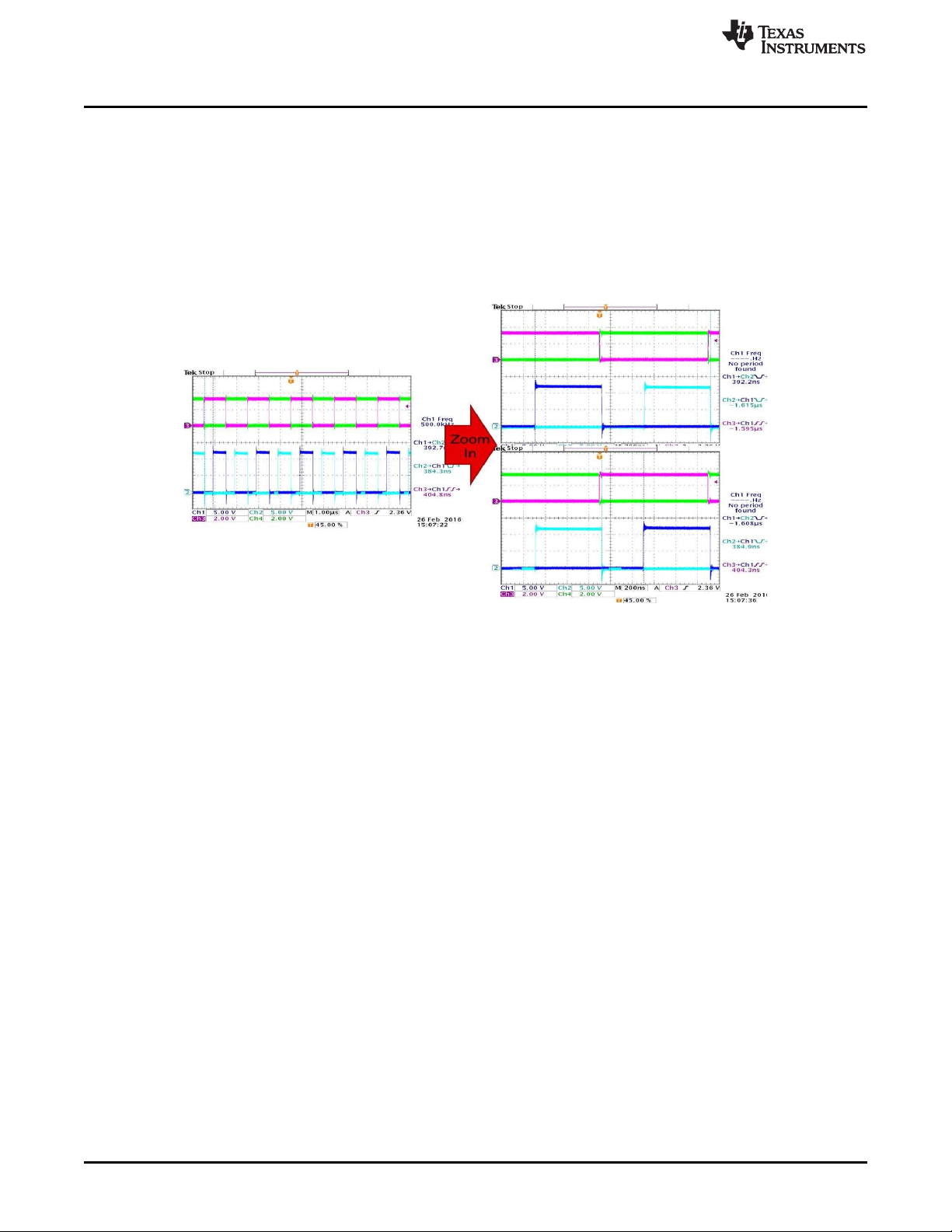
7.1 DT Connected to VCCI(J-DT Option B in Table 2)
The dead time (DT) between the outputs of the two channels is decided by inputs (see Figure 4). Overlap
between two output channels is allowed. Figure 4 shows a waveform with overlapped operations.
Figure 4. Overlap is Allowed When DT Connected to VCCI
(Channels 3 and 4 are PWM Inputs, Channels 1 and 2 are Driver Outputs)
7.2 DT Pin Floating or Left Open (J-DT Option A in Table 2)
The dead time (DT) between the outputs of the two channels is around 8 ns, which is preset for interlock
protections (see Figure 5).
Figure 5. Test Waveforms if DT is Left Open
(Channel 3 and 4 are PWM Inputs, and Channel 1 and 2 are Driver Outputs)
SLUUBG8B–June 2016–Revised November 2018
Submit Documentation Feedback
Copyright © 2016–2018, Texas Instruments Incorporated
Using the UCC21520EVM-286, UCC20520EVM-286, UCC21521CEVM-286,
and UCC21530EVM-286
11
Page 12
Test Waveforms (CL=0pF) With Different DT Configurations
7.3 DT Pin Connected to RDT (J-DT Option C in Table 2)
The dead time (DT) between the outputs of the two channels is set according to: DT (in ns) = 10 × RDT
(in kΩ).
The steady-state voltage at DT pin is around 0.8 V, and the DT pin current will be less than 10 µA when
RDT= 100 kΩ. Therefore, TI recommends to parallel a ceramic bypass capacitor (2.2 nF or above) with
RDTto achieve better noise immunity and better dead-time matching between two channels, especially
when the dead time is larger than 300 ns. The major consideration is that the current through the RDTis
used to set the dead time, and this current decreases as RDTincreases. This bypass capacitor is not
installed in the EVM, but the user can easily install it on the bottom layer where the RDTis located.
www.ti.com
Figure 6. Test Waveforms if DT Connected to R
DT
(Channel 3 and 4 is PWM Inputs, and Channel 1 and 2 is Driver Outputs)
12
Using the UCC21520EVM-286, UCC20520EVM-286, UCC21521CEVM-286,
and UCC21530EVM-286
Copyright © 2016–2018, Texas Instruments Incorporated
SLUUBG8B–June 2016–Revised November 2018
Submit Documentation Feedback
Page 13

0.22µF
C11
0.22µF
C12
0.22µF
C13
1µF
C14
1µF
C15
GND
GNDA
GNDB
GNDA
GNDB
1
2
J1
1727010
1
2
3
J-INA
TSW-103-07-G-S
1
2
3
J-INB
TSW-103-07-G-S
1
2
3
J-DIS
TSW-103-07-G-S
1
2
3
J-DT
TSW-103-07-G-S
GND
GND
GND
VCCIN VCC
VCC
VCC
GND
GND
DT
VCC
VCC
GND
INA
INB
1.00
R11
0
R_LB
GNDA
GNDB
GNDA
GNDB
GND
OUTA
OUTB
V_GA
VDDAIN
V_GB
VDDBIN
DISABLE
VCC
VDDA
VDDB
1
2
3
J2
1727023
1
2
3
J3
1727023
TP1
TP2
TP3
TP4
TP5
TP6
TP7
TP8
TP10
TP11
TP13
TP14
TP15
TP16
TP20
TP0
0
R_LA
1000pF
CL_A
1000pF
CL_B
GND
GND
GND
GND
GND
TP19
10pF
C1
10pF
C2
2.2
R12
2.2
R13
10µF
CIN
10µF
C16
100k
RDT
3266W-1-104LF
JINA
JINB
TP9
TP12
TP17
2.2
RB
i Ch-A
ClassName: Ch-A
i Ch-B
ClassName: Ch-B
GNDA
GNDB
INA
1
INB
2
VCCI
3
GND
4
DISABLE
5
DT
6
NC
7
VCCI
8
VSSB
9
OUTB
10
VDDB
11
NC
12
NC
13
VSSA
14
OUTA
15
VDDA
16
U1
UCC21520DW
VDDB
51
R4
51
R5
1
4
3
DB
C3D02060E
www.ti.com
8 Schematic
Figure 7 only shows the schematic diagram for UCC21520EVM. The schematic diagrams for the UCC20520EVM, UCC21521CEVM, and
UCC21530EVM are similar to Figure 7, with the exception that the device under test (U1) could be in one of the following driver ICs:
UCC21520DW, UCC20520DW, UCC21521CDW, or UCC21530DWK.
Schematic
SLUUBG8B–June 2016–Revised November 2018
Submit Documentation Feedback
Figure 7. UCC21520EVM-286 Schematic
Using the UCC21520EVM-286, UCC20520EVM-286, UCC21521CEVM-286,
Copyright © 2016–2018, Texas Instruments Incorporated
13
and UCC21530EVM-286
Page 14

Layout Diagrams
9 Layout Diagrams
The PCB layout information for UCC21520EVM is shown in Figure 8, Figure 9, Figure 10, and Figure 11.
The layouts are the same for UCC20520EVM, UCC21521CEVM, and UCC21530EVM except for the
labels that designate the EVM part number with the device under test.
www.ti.com
Figure 8. Top Overlay
14
Figure 9. Top Layer
Using the UCC21520EVM-286, UCC20520EVM-286, UCC21521CEVM-286,
and UCC21530EVM-286
Copyright © 2016–2018, Texas Instruments Incorporated
SLUUBG8B–June 2016–Revised November 2018
Submit Documentation Feedback
Page 15

www.ti.com
Layout Diagrams
Figure 10. Bottom Layer
SLUUBG8B–June 2016–Revised November 2018
Submit Documentation Feedback
Copyright © 2016–2018, Texas Instruments Incorporated
Figure 11. Bottom Overlay
Using the UCC21520EVM-286, UCC20520EVM-286, UCC21521CEVM-286,
and UCC21530EVM-286
15
Page 16

List of Materials
10 List of Materials
QTY DES DESCRIPTION MANUFACTURE PART NUMBER
2 C1, C2 Capacitor, ceramic, 10 pF, 50 V, ±5%, C0G/NP0, 0603. C2 is
3 C11, C12,
C13
2 C14, C15 Capacitor, ceramic, 1 μF, 50 V, ±10%, X5R, 0603 Std Std
2 C16, CIN Capacitor, ceramic, 10 μF, 50 V, ±10%, X5R, 1206_190 Std Std
0 CL_A, CL_B Capacitor, ceramic, 1000 pF, 50 V, ±5%, C0G/NP0, 0805 Not Populated Not Populated
0 DB Diode, Schottky, 600 V, 8 A, DPAK Not Populated Not Populated
4 H1, H2, H3,H4Machine screw, round, #4-40 x 1/4, nylon, philips panhead Std Std
4 H5, H6, H7,H8Standoff, hex, 0.5"L #4-40 nylon Std Std
www.ti.com
Table 6. UCC2x5xxEVM-286 List of Materials
Std Std
not populated in UCC20520EVM.
Capacitor, ceramic, 0.22 μF, 50 V, ±10%, X7R, 0603 Std Std
4 J-DIS, J-DT,
J-INA, J-INB
1 J1 Connection terminal block, 2 position, 3.81 mm, TH Std Std
2 J2, J3 Terminal block receptacle, 3 × 1, 3.81 mm, R/A, TH Std Std
15 JINA, JINB,
TP0, TP1,
TP2, TP3,
TP4, TP5,
TP6, TP7,
TP8, TP9,
TP10, TP11,
TP12
0 R4, R5 Resistor, 51 Ω, 5%, 0.1 W, 0603 Not Populated Not Populated
1 R11 Resistor, 1.00 Ω, 1%, 0.125 W, 0805 Std Std
2 R12, R13 Resistor, 2.2 Ω, 5%, 0.1 W, 0603 Std Std
1 RB Resistor, 2.2 Ω, 5%, 0.125 W, 0805 Std Std
2 R_LA, R_LB Resistor, 0 Ω, 5%, 0.125 W, 0805 Std Std
1 RDT Trimmer, 100 kΩ, 0.25 W, TH Std Std
2 SH1, SH2 Shunt, 100 mil, flash gold, black Std Std
6 TP13, TP14,
TP15, TP16,
TP19, TP20
1 TP17 Test point, miniature, SMT Std Std
1 U1 UCC21520DW, UCC20520DW, UCC21521CDW and
Header, 100 mil, 3 × 1, gold, TH. J-INB is not installed in
UCC20520EVM.
Test point, miniature, red, TH. JINB and TP4 are not installed
in UCC20520EVM.
Test point, miniature, black, TH. TP15 is not installed in
UCC20520EVM.
UCC21530DWK, 4-A and 6-A, 5-KV
Universal Gate Driver, DW0016A and DWK0014 for
UCC21530DWK
Dual Isolated-channel
RMS
Std Std
Std Std
Std Std
Texas Instruments UCC21520DW,
UCC20520DW,
UCC21521CDW,
or UCC21530DWK
16
Using the UCC21520EVM-286, UCC20520EVM-286, UCC21521CEVM-286,
and UCC21530EVM-286
Copyright © 2016–2018, Texas Instruments Incorporated
SLUUBG8B–June 2016–Revised November 2018
Submit Documentation Feedback
Page 17

www.ti.com
Revision History
Revision History
NOTE: Page numbers for previous revisions may differ from page numbers in the current version.
Changes from A Revision (November 2016) to B Revision ........................................................................................... Page
• Added device type to include the UCC21530EVM-286 Evalustion Module ....................................................... 4
Changes from Original (June 2016) to A Revision ......................................................................................................... Page
• Added device type to include the UCC20520EVM-286 and UCC21521CEVM-286 Evalustion Modules ..................... 4
SLUUBG8B–June 2016–Revised November 2018
Submit Documentation Feedback
Copyright © 2016–2018, Texas Instruments Incorporated
Revision History
17
Page 18

IMPORTANT NOTICE AND DISCLAIMER
TI PROVIDES TECHNICAL AND RELIABILITY DATA (INCLUDING DATASHEETS), DESIGN RESOURCES (INCLUDING REFERENCE
DESIGNS), APPLICATION OR OTHER DESIGN ADVICE, WEB TOOLS, SAFETY INFORMATION, AND OTHER RESOURCES “AS IS”
AND WITH ALL FAULTS, AND DISCLAIMS ALL WARRANTIES, EXPRESS AND IMPLIED, INCLUDING WITHOUT LIMITATION ANY
IMPLIED WARRANTIES OF MERCHANTABILITY, FITNESS FOR A PARTICULAR PURPOSE OR NON-INFRINGEMENT OF THIRD
PARTY INTELLECTUAL PROPERTY RIGHTS.
These resources are intended for skilled developers designing with TI products. You are solely responsible for (1) selecting the appropriate
TI products for your application, (2) designing, validating and testing your application, and (3) ensuring your application meets applicable
standards, and any other safety, security, or other requirements. These resources are subject to change without notice. TI grants you
permission to use these resources only for development of an application that uses the TI products described in the resource. Other
reproduction and display of these resources is prohibited. No license is granted to any other TI intellectual property right or to any third
party intellectual property right. TI disclaims responsibility for, and you will fully indemnify TI and its representatives against, any claims,
damages, costs, losses, and liabilities arising out of your use of these resources.
TI’s products are provided subject to TI’s Terms of Sale (www.ti.com/legal/termsofsale.html) or other applicable terms available either on
ti.com or provided in conjunction with such TI products. TI’s provision of these resources does not expand or otherwise alter TI’s applicable
warranties or warranty disclaimers for TI products.
Mailing Address: Texas Instruments, Post Office Box 655303, Dallas, Texas 75265
Copyright © 2018, Texas Instruments Incorporated
 Loading...