10/94
Note: Pin numbers refer to PLCC packag e.
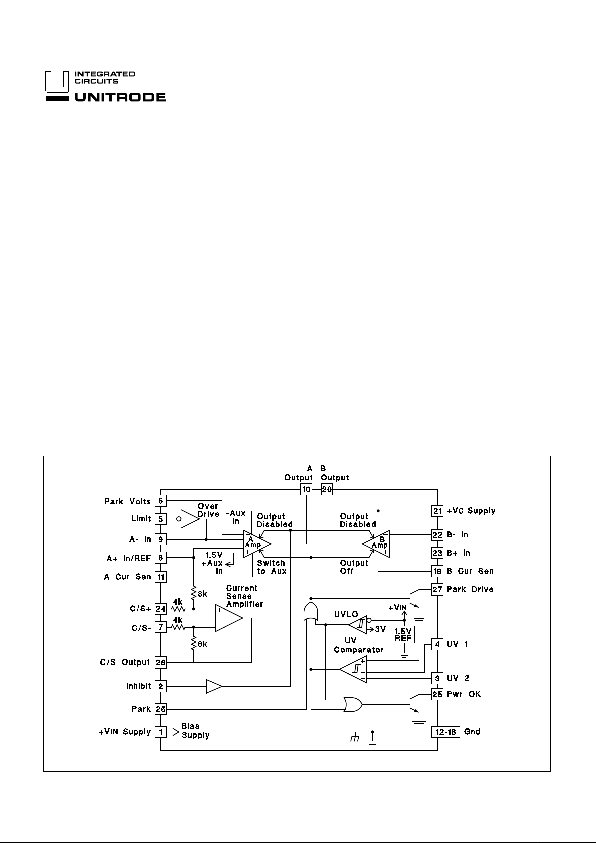
BLOCK DIAGRAM
• Precision Current Control
•
±
800mA Load Current
• 1.25V Total V
SAT at 800mA
• Controlled Velocity Head Parking
• Precision Dual Supply Monitor
with Indicator
• Limit Input to Force Output
Extremes
• Inhibit Input and UVLO
• 4V to 15V operation
This full-bridge power amplifier is rated for continuous output current of 0.8 Amperes and is intended for use in demanding servo applications such as head
positioning for high-d ensi ty disk drives. The device includes a precision current
sense amplifier that provides accurate control of load current. Current is
sensed with a single resi s tor in seri es with the load. The power amplifier has a
very low output saturation voltage and will operate down to 4V supply levels.
Power output stage protection includes current l imiting and thermal shutdown.
Auxiliary functions on this device include a dual-input under-voltage comparator, which can monitor two independent supply voltages and force a built-in
head park function when either is below minimum. When activated by e ither the
UV comparator, or a command at the separate PARK input, the park circuitry
will override the amplifier i nputs to convert the power outputs to a programmable constant voltage source which will h old regula tion as th e supply voltage
falls to below 3.0 Volts. Added features include a POWER OK flag output, a
LIMIT input to force the drive output to its maximum level in either polarity, and
a over-riding INHIBIT input to disable al l amplifiers and reduce quiescent supply current.
This device is packaged in a power PLCC surface mount configuration which
maintains a standard 28-pin outline, but with 7 pins along one edge allocated to
ground for optimum thermal transfer. And is also available in a 24-pin surface
mount SOIC package.
UC3175B
Full-Bridge Power Amplifier
FEATURES DESCRIPTION
UDG-92054-1

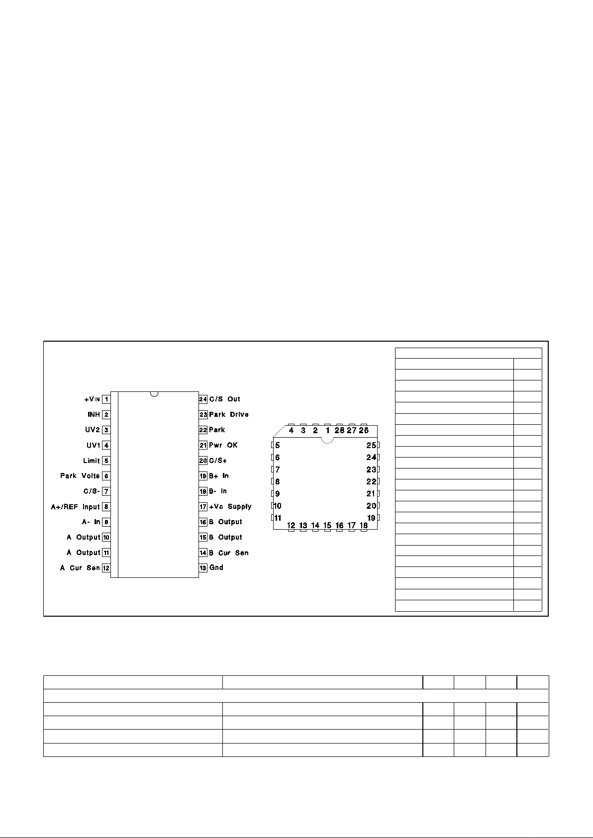
CONNECTION DIAG RAMS
UC3175B
PACKAGE PIN FUNCTION
FUNCTION PIN
+VIN 1
INH 2
UV2 3
UV1 4
Limit 5
Park Volts 6
C/S- 7
A+/REF Input 8
A- In 9
A Output 10
A Cur Sen 11
Gnd (Heat Dissipat io n Pins) 12-18
B Cur Sen 19
B Output 20
+V
C Supply 21
B- In 22
B+ In 23
C/S+ 24
Pwr OK 25
Park 26
Park Drive 27
C/S Out 28
PLCC-28 (Top View)
QP Package
ABSOLUTE MAXIMUM RATINGS
Input Supply Vo ltag e, (+VIN,+VC). . . . . . . . . . . . . . . . . . . . . . . . . . . . . . . . 20V
UV Comparator, and Digital Input s
Maximum forced vo ltag e. . . . . . . . . . . . . . . . . . . . . . . . . . . . . -0.3V to 10V
Maximum forced cu rrent. . . . . . . . . . . . . . . . . . . . . . . . . . . . . . . . . ±10mA
C/S Inputs
Maximum forced vo ltag e. . . . . . . . . . . . . . . . . . . . . . . . . . . . . -0.3V to 20V
A and B Amplifier Inpu ts . . . . . . . . . . . . . . . . . . . . . . . . . . . . -0.3V to +V
IN
Open Collector Out put Voltages. . . . . . . . . . . . . . . . . . . . . . . . . . . . . . . . . 20V
A and B Output Curren ts (continu ous)
Source . . . . . . . . . . . . . . . . . . . . . . . . . . . . . . . . . . . . . . . Internally Limited
Sink . . . . . . . . . . . . . . . . . . . . . . . . . . . . . . . . . . . . . . . . . . . . . . . . . . . 1.0A
Parking Drive Output Curr ent
Continuous . . . . . . . . . . . . . . . . . . . . . . . . . . . . . . . . . . . . . . . . . . . 150mA
Pulsed . . . . . . . . . . . . . . . . . . . . . . . . . . . . . . . . . . . . . . . . . . . . . . . . . . . 1A
Output Diode Current (pulsed). . . . . . . . . . . . . . . . . . . . . . . . . . . . . . . . . . . 1A
Power OK Output Cu rrent (c ont inuou s) . . . . . . . . . . . . . . . . . . . . . . . . . 30mA
Operating Jun ctio n Tem per atur e. . . . . . . . . . . . . . . . . . . . . . -55°C to +150 °C
Storage Temperature . . . . . . . . . . . . . . . . . . . . . . . . . . . . . . . -65°C to +150°C
Note 1: Unless other w ise indicat ed, volt age s are
reference d to grou nd and current s are pos itive
into, negat ive out of, the sp ecif ied te rminals.
"Pulsed" is defined as a less than 10% duty cycle
pulse with a maximum dur ation of 500µs.
Note 2: See Unitrode Int egr at ed Circ uits databoo k
for informat ion regarding thermal specif ic atio ns
and limitat ions of packages.
PARAMETER TEST CONDITION S MIN TYP MAX UNITS
INPUT SUPPLY
+V
IN Supply Current All Amplifier Outpu ts = 6V 35 42 mA
+V
C Supply Current IOUT = 0A 1 mA
+V
IN UVLO Threshold Low to High 2.8 3.0 V
UVLO Threshold Hysteresis 200 mV
ELECTRICAL CHARACTERISTICS:
Unless otherwise stated spec ifications apply for 0°C ≤ TA ≤ 70°C, +VIN = 12V, +VC
= +VIN, A+/REF Inp ut = 6 V. TA=TJ.
SOIC-24 (Top View)
DW Package
Thermal Data
QP Package:
Thermal Resistance Junction to Leads,
θ
JL . . . . . . . . . . . . . . . . . . . . . . . 15°C/W
Thermal Resistance Junction to Ambient,
θ
JA . . . . . . . . . . . . . . . . . . . . . . . 40°C/W
2
 Loading...