

6/98
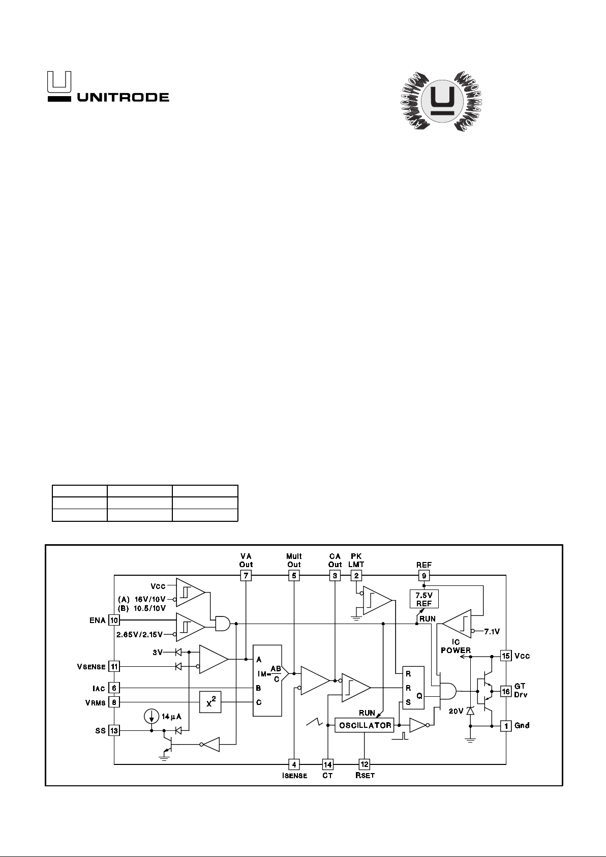
BLOCK DIAGRAM
• Controls Boost PWM to Near Unity
Power Fac tor
• Limits Line Current Distortion To <3%
• World-Wide Operation Without Switches
• Accurate Power Limiting
• Fixed Frequency Average Current Mode
Control
• High Bandwidth (5MHz), Low Offset
Current Am p lifier
• Integrated Current and Voltage Amp
Output Clamps
• Multiplier Improvem ents: Linearity,
500mV VAC Offset (eliminates external
resistor), 0-5V Multout Common Mode
Range
• V
REF
"GOOD" Comparator
• Faster and Improved Accuracy ENABLE
Comparator
• UVLO Threshold Options
(16/10V / 10.5/10V)
• 300µA Startup Supply Current
The UC1854A/B pro duct s are pin compatible enhan ced versi ons of the
UC1854. Li ke the UC1854, these pr oducts prov ide all of the functions
necessary for active power factor corrected preregulators. The
controller achieves near unity power factor by shaping the AC input line
current wav ef or m to corres pond to the AC input line voltage. To do this
the UC185 4A/B uses a verage current mode control. Average c urrent
mode control maintains stable, low distortion sinusoidal line current
without the need for slope compensation, unlike peak current mode
control.
The UC1854A/B products i mprove upon t he UC 1854 by offering a wide
bandwidth, low offset Current Amplifier, a faster responding and
improved accuracy enable comparator, a V
REF
"good" comparator,
UVLO thresh old options (16/ 10V for offline, 10.5/10V for startup from
an auxiliary 12V regulator), lower startup supply current, and an
enhanced m ultiply/ divide circui t. New featu res like the ampli fier output
clamps, improved amplifier current sinking capability, and low offset
VAC pin reduce the external component count while improving
performance. Improved common mode input range of the Multiplier
output/Current Amp input allow the designer greater flexibility in
choosing a method for current sensing. U nlike its pre decessor, R
SET
controls onl y oscillator charging curr ent and has no effect on clamping
the maximum multiplier output curr ent. This current is no w clamped to
a maximu m of 2 * IAC at all t imes which simplifies the desi gn process
and pro vides foldb ack power lim iting dur ing brow nout and extrem e low
line conditions.
A 1% 7.5V reference, fixed frequency oscillator, PWM, Voltage
Amplifier w ith softstar t, line voltage feedforwar d (V
RMS
squarer) , input
supply vol tage clamp, and over current com par ator roun d out the list of
features.
UC1854A/B
UC2854A/B
UC3854A/B
Enhanced High Power Factor Preregulator
FEATURES
DESCRIPTION
UVLO Turn on UVLO Turn off
UC1854A 16V 10V
UC1854B 10.5V 10V
UDG-93001-1
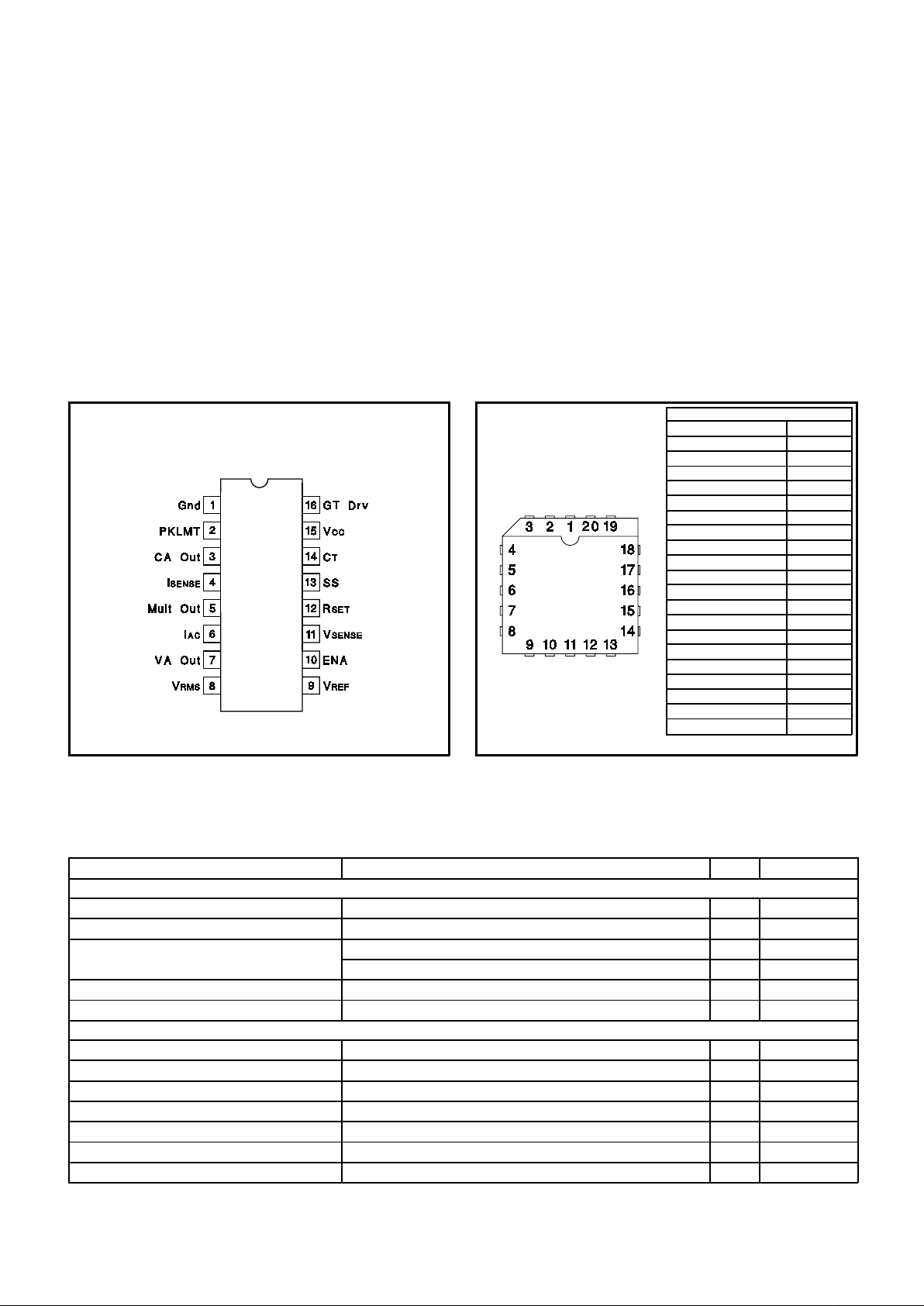
DIL–16 & SOIC-16
(Top V ie w )
J, N & DW Packages
PACKAGE PIN FUNCTION
FUNCTION PIN
N/C 1
Gnd 2
PKLMT 3
CA Out 4
I
SENSE
5
N/C 6
Mult Out 7
I
AC
8
VA Out 9
V
RMS
10
N/C 11
V
REF
12
ENA 13
V
SENSE
14
R
SET
15
N/C 16
SS 17
C
T
18
V
CC
19
GT Drv 20
PLCC-20 & LCC-20
(Top View)
Q & L Packages
CONNECTION DIAGRAMS
Supply Voltage VCC. . . . . . . . . . . . . . . . . . . . . . . . . . . . . . 22V
GT Drv Current, Continuous. . . . . . . . . . . . . . . . . . . . . . . 0.5A
GT Drv Current, 50% Duty Cycle. . . . . . . . . . . . . . . . . . . . 1.5A
Input Voltage, V
SENSE
, V
RMS
. . . . . . . . . . . . . . . . . . . . . . . 11V
Input Voltage, I
SENSE
, Mult Out . . . . . . . . . . . . . . . . . . . . . 11V
Input Voltage, PKLMT . . . . . . . . . . . . . . . . . . . . . . . . . . . . . 5V
Input Current, R
SET
, IAC, PKLMT, ENA . . . . . . . . . . . . . . 10mA
Power Dissipation . . . . . . . . . . . . . . . . . . . . . . . . . . . . . . . . 1W
Storage Temperature . . . . . . . . . . . . . . . –65°C to +150°C
Lead Temperature (Soldering, 10 Seconds) . . . . . . . . . +300°C
ABSOLUTE MAXIMUM RATINGS
UC1854A/B
UC2854A/B
UC3854A/B
Note 1: All voltages with respect to Gnd (Pin 1).
Note 2: All currents are positive into the specified terminal.
Note 3: ENA imput is internally clamped to approximately 10V.
Note 4: Consult Unitrode Integrated Circuits databook for
information regarding thermal specifications and limitations of
packages.
PARAMETER TEST CONDITIONS MIN TYP MAX UNITS
OVERALL
Supply Current, Off CAO, VAO = 0V, VCC = UVLO - 0.3V 250 400 µA
Supply Current, On 12 18 mA
VCC Turn-On Threshold UC1854A 16 17.5 V
UC1854B 10.5 11.2 V
VCC Turn-Off Threshold UC1854A / B 9 10 V
V
CC
Clamp I(VCC) = ICC(on) + 5mA 18 20 22 V
VOLTAGE AMPLIFIER
Input Voltage 2.9 3.0 3.1 V
V
SENSE
Bias Current –500 –25 500 nA
Open Loop Gain V
OUT
= 2 to 5V 70 100 dB
V
OUT
High I
LOAD
= –500µA6V
V
OUT
Low I
LOAD
= 500µA 0.3 0.5 V
Output Short Circuit Current V
OUT
= 0V 1.5 3.5 mA
Gain Bandwidth Product Fin = 100kHz, 10mV p-p, (Note 1) 1 mHz
Unless otherwise stated, V
CC
=18V, RT=8.2k, CT=1.5nF, PKLMT=1V, V
RMS
=1.5V,
I
AC
=100µA, I
SENSE
=0V, CA Out=3.5V, VA Out=5V, V
SENSE
=3V, –55oC<TA<125oC
for the UC1854A/B, –40
o
C<TA<85oC for the UC2854A/B, and 0oC<TA<70oC for the
UC3854A/B, and T
A=TJ
.
ELECTRICAL CHARACTERISTICS
2
ELECTRICAL
CHARACTERISTICS (cont.)
PARAMETER TEST CONDITIONS MIN TYP MAX UNITS
CURRENT AMPLIFIER
Input Offset Voltage V
CM
= 0V TA = +25°C −40mV
OverTemp –5.5 0 mV
Input Bias Current(sense) VCM = 0V –500 500 nA
Open Loop Gain VCM = 0V, V
OUT
= 2 to 6V 80 110 dB
V
OUT
High I
LOAD
= –500µA8V
V
OUT
Low ILOAD = 500µA 0.3 0.5 V
Output Short Circuit Current V
OUT
= 0V 1.5 3.5 mA
Common Mode Range –0.3 5 V
Gain Bandwidth Product Fin = 100kHz, 10mV p-p, (Note 1) 3 5 mHz
REFERENCE
Output Voltage I
REF
= 0mA, TA = 25oC 7.4 7.5 7.6 V
I
REF
= 0mA 7.35 7.5 7.65 V
Load Regulation I
REF
= 1 to 10mA 0 8 20 mV
Line Regulation V
CC =
12 to 18V 0 14 25 mV
Short Circuit Current V
REF
= 0V 25 35 60 mA
OSCILLATOR
Initial Accuracy TA = 25oC 85 100 115 kHz
Voltage Stability V
CC =
12 to 18V 1 %
Total Variation Line, Temp 80 120 kHz
Ramp Amplitude (p-p) 4.9 5.9 V
Ramp Valley Voltage 0.8 1.3 V
ENABLE / SOFTSTART / CURRENT LIMIT
Enable Threshold 2.35 2.55 2.8 V
Enable Hysteresis V
FAULT
= 2.5V 500 600 mV
Enable Input Bias Current V
ENABLE
= 0V –2 –5 µA
Propagation Delay to Disable Enable Overdrive = –100mV,(Note 1) 300 ns
SS Charge Current V
SOFTSTART
= 2.5V 10 14 24
PKLMT Offset Voltage –15 15 mV
PKLMT Input Current V
PKLMT
= –0.1V –200 –100 µA
PKLMT Propagation Delay (Note 1) 150 ns
MULTIPLIER
Output Current - IAC Limited IAC=100µA, V
RMS
= 1V, R
SET
= 10k –220 –200 –170 µA
Output Current - Zero IAC=0µA, R
SET
= 10k –2.0 –0.2 2.0 µA
Output Current - Power Limited V
RMS
= 1.5V, Va = 6V –230 –200 –170 µA
Output Current V
RMS
= 1.5V, Va = 2V –22 µA
V
RMS
= 1.5V, Va = 5V –156 µA
V
RMS
= 5V, Va = 2V –2 µA
V
RMS
= 5V, Va = 5V –14 µA
Gain Constant (Note 2) V
RMS
= 1.5V, TJ = 25°C, Va = 6V –1.1 –1.0 –0.9 A/A
UC1854A/B
UC2854A/B
UC3854A/B
Unless otherwise stated, VCC=18V, RT=8.2k, CT=1.5nF, PKLMT=1V, V
RMS
=1.5V,
I
AC
=100µA, I
SENSE
=0V, CA Out=3.5V, VA Out=5V, V
SENSE
=3V, –55oC<TA<125oC for the
UC1854A/B, –40
o
C<TA<85oC for the UC2854A/B, and 0oC<TA<70oC for the UC3854A/B,
and T
A=TJ
.
Note 1: Guaranteed by design, not 100% tested in production.
Note 2: Gain constant (K) =
I
AC
× (Va − 1.5
V
)
V
RMS
2 ×
I
MO
3

PARAMETER TEST CONDITIONS MIN TYP MAX UNITS
GATE DRIVER
Output High Voltage I
OUT
= –200mA, VCC = 15V 12 12.8 V
Output Low Voltage I
OUT
= 200mA 1 2.2 V
I
OUT
= 10mA 300 500 mV
Output Low (UVLO) I
OUT
= 50mA, VCC = 0V 0.9 1.5 V
Output Rise / Fall Time C
LOAD
= 1nF, (Note 1) 35 ns
Output Peak Current C
LOAD
= 10nF, (Note 1) 1.0 A
UC1854A/B
UC2854A/B
UC3854A/B
Note 1: Guaranteed by design, not 100% tested in production.
Note 2: Gain constant (K) =
I
AC
× (Va − 1.5
V
)
V
RMS
2 ×
I
MO
ELECTRICAL
CHARACTERISTICS (cont.)
Unless otherwise stated, VCC=18V, RT=8.2k, CT=1.5nF, PKLMT=1V, V
RMS
=1.5V, IAC=100µA,
I
SENSE
=0V, CA Out=3.5V, VA Out=5V, V
SENSE
=3V, –55oC<TA<125oC for the UC1854A/B,
–40
o
C<TA<85oC for the UC2854A/B, and 0oC<TA<70oC for the UC3854A/B, and TA=TJ.
The UC1854A/B products were designed as pin
compatible upgrades to the industry standard UC1854
active Power Factor correction circuits. The circuit
enhancem ents a llow the use r to el iminat e in m ost cases
several external components currently required to
successfully apply the UC1854. In addition, linearity
improve me nts to the Mul ti pl y, Square, and D ivid e circ uitry
optimizes overall system performance. Detailed
descriptions of the circuit enhancements are provided
below. For in-depth design applications reference data
refer to Unitrode application notes U-134 and DN-44.
MULTIPLY / SQUARE AND DIVIDE
The UC1854A/B Multiplier design maintains the same
gain constant (K = −1), as the U C1854. The relations hip
between the inputs and output current is given as:
IMO = IAC(VAO - 1.5V) / K•V
RMS
2
This is nearly the same as the UC1854, but circuit
differences have improved the performance and
application.
The firs t difference is with the IAC input. The U C1854A/B
regulates this pin voltage to a nominal 500mV over the full
operating temperature range, rather than the 6.0V used
on the UC1854. This low offset voltage eliminates the
need for a line zero crossing compensating resistor to
V
REF
from IAC that UC1854 designs require. The
maximum current at high line into IAC shoul d be limited t o
250µA for best performance. Therefore, if VAC (max) =
270V, then RAC = 270(1.414) / 250µA = 1.53MΩ.
The V
RMS
pin linear operating ra nge is improved with the
UC1854A/B as well. The input range for V
RMS
extends
from 0 to 5.5V. Since the UC1854A squaring circuit
employs an analog multiplier, rather than a linear
approxim ation, accuracy i s improved, and dis continuities
are eliminated. Th e external divider networ k c onnected to
V
RMS
should produc e 1.5V at low line (85VAC). This will
put 4.77V on V
RMS
at high line (27VAC) which is well
within its operating range.
The Voltage Ampl ifier outpu t form s the third input t o the
Multiplier and is internally clamped to 6.0V. This
eliminates an ext ernal zener clamp often u sed in UC1854
designs. The offset voltage at this input to the Multiplier
has been raised on the UC1854A/B to 1.5V.
The Multiplier output pin, which is also common to the
Current Am pl if ie r n on- inverting input, has a −0.3V to 5.0V
output range,compared to the −0.3 to 2.5V range of the
UC1854. This im prov ement al lows t he UC1854A/ B to be
used in applications where the current sense signal
amplitude is very large.
VOLTAGE AM PLIFIE R
The UC1854A/B Voltage Amplifier design is essentially
similar to the UC1854 with two exceptions. The first is with
the internal connection. The lower voltage reduces the
amount of charge on the compensation capacitor, which
provides improved recovery from large signal events,
such as line dropouts, or power interruption. It also
minimizes the DC current flowing through the feedback.
The output of the Voltage amplifier is also changed. In
addition to a 6.0V temperature compensated clamp, the
output short circuit current has been lowered to 2mA
typical, and an act ive pull down has replaced the passive
pulldown of the UC1854.
CURRENT AM PLIFIE R
The Current Amplifier for an average current PFC
controll er needs a low offset v oltage i n order to minimize
AC line current distortion. With this in mind, the
UC1854A/B Current Amplifier has improved the input
offset voltage from ±4mV to 0 to −3mV. The negative
FUNCTIONAL DESCRIPT ION
4

offset of the UC1854A/ B guarantees that the PWM circuit
will not dr ive the M OS FET if t he cur ren t command is ze ro
(both Current amplifier inputs zero.).Previous designs
required an external offset cancellation network to
implement this key f eature. The bandw idth of the Current
Amplifier has been improved as well to 5mHz typical.
While this i s not generally an issue at 50 or 60Hz inputs, it
is essential for 400Hz input avionics applications.
MISC ELL ANEO US
Several other important enhancements have been
implemented in the UC1854A/B. A VCC supply voltage
clamp at 20V allows the controller to be current fed if
desired. The lower star tup supply c urrent ( 250µA typical),
substa nti ally reduces the power requireme nts of an offline
startup resistor. The 10.5/10V UVLO option (UC1854B)
enables the controller to be powered off of an auxiliary
12V supply .
The V
REF
"GOOD" comparator guarantees that the
MOSFET driver output remains low if the supply or the
7.5V reference are not yet up. This improvement
eliminates the need for external Schottky diodes on the
PKL and CA+ pins that some UC1854 de signs require.
The propagation delay of the disable feature has been
impro ved to 300ns typic al. This delay was proportional to
FUNCTIONAL DESCRIPT ION (cont.)
UC1854A/B
UC2854A/B
UC3854A/B
TYPICAL CHARACTERIS TICS at T
A
= TJ = 25°C
Load Capacitance,µF
ns
0
100
200
300
400
500
600
700
0 0.01 0.02 0.03 0.04 0.05
Rise Time
Fall Time
Gate Drive Rise and Fall Time
R
SET
, k
Ω
Duty
Cycle
70%
75%
80%
85%
90%
95%
100%
1 10 100
Gate Drive Maximum Duty Cycle
0 50 100 150 200 250
0.8
0.84
0.88
0.92
0.96
1
1.04
1.08
1.12
1.16
1.2
K
IACCurrent (µA)
V
RMS
=
1.5V
V
RMS
=
3.0V
V
RMS
=
5.0V
UC1854A/B Multipli er Linearity
VA
OUT
= 3.5V
0 50 100 150 200 250
0.8
0.84
0.88
0.92
0.96
1
1.04
1.08
1.12
1.16
1.2
K
I
AC
Current (µA)
V
RMS
=
3.0V
V
RMS
=
1.5V
V
RMS
=
5.0V
UC1854A/B Multiplier Linearity
VA
OUT
= 5V
5

TYPICAL CHARACTERIS TICS at TA = TJ = 25°C (cont.)
UNITRODE CORP ORA TION
7 CONTINENTAL BLVD . • MER RIMACK, NH 03054
TEL. (603) 424-2410 FAX (603) 424-3460
These product s conta in patent ed circuitry and are sold under li cense from Pi oneer M agnet ics, Inc.
UC1854A/B
UC2854A/B
UC3854A/B
log f
Gain (dB)
-60
-40
-20
0
20
40
60
0
80
-45
Phase
Degrees
100
-90
120
10kHz 1MHz 10MHz
100kHz
Gain
Phase
5.992 496 516 MHz
Current Amplifier Frequency Response
R
SET
, k Ω
Frequency
kHz
10
100
1000
1
10
100
100pF
200pF
5nF
10nF
3nF
500pF
2nF
1nF
Oscill ator Frequency vs R
SET
and C
T
Frequency
kHz
Phase
Margin
degrees
Open-Loop
Gain
dB
-20
0
20
40
60
80
100
120
0.1 1 10 100 1000 10000
Voltage Amplifier Gain and Phase vs Frequency
6

IMPORTANT NOTICE
T exas Instruments and its subsidiaries (TI) reserve the right to make changes to their products or to discontinue
any product or service without notice, and advise customers to obtain the latest version of relevant information
to verify, before placing orders, that information being relied on is current and complete. All products are sold
subject to the terms and conditions of sale supplied at the time of order acknowledgement, including those
pertaining to warranty, patent infringement, and limitation of liability.
TI warrants performance of its semiconductor products to the specifications applicable at the time of sale in
accordance with TI’s standard warranty. Testing and other quality control techniques are utilized to the extent
TI deems necessary to support this warranty. Specific testing of all parameters of each device is not necessarily
performed, except those mandated by government requirements.
CERT AIN APPLICATIONS USING SEMICONDUCTOR PRODUCTS MAY INVOLVE POTENTIAL RISKS OF
DEATH, PERSONAL INJURY, OR SEVERE PROPERTY OR ENVIRONMENTAL DAMAGE (“CRITICAL
APPLICATIONS”). TI SEMICONDUCTOR PRODUCTS ARE NOT DESIGNED, AUTHORIZED, OR
WARRANTED TO BE SUITABLE FOR USE IN LIFE-SUPPORT DEVICES OR SYSTEMS OR OTHER
CRITICAL APPLICATIONS. INCLUSION OF TI PRODUCTS IN SUCH APPLICA TIONS IS UNDERSTOOD T O
BE FULLY AT THE CUSTOMER’S RISK.
In order to minimize risks associated with the customer’s applications, adequate design and operating
safeguards must be provided by the customer to minimize inherent or procedural hazards.
TI assumes no liability for applications assistance or customer product design. TI does not warrant or represent
that any license, either express or implied, is granted under any patent right, copyright, mask work right, or other
intellectual property right of TI covering or relating to any combination, machine, or process in which such
semiconductor products or services might be or are used. TI’s publication of information regarding any third
party’s products or services does not constitute TI’s approval, warranty or endorsement thereof.
Copyright 1999, Texas Instruments Incorporated
 Loading...