

High Power Factor Preregulator
UC1853
UC2853
UC3853
FEATURES
• Complete 8-pin Power Factor
Solution
• Reduced External Components
• RMS Line Voltage Compensation
• Precision Multiplier/Squarer/Divider
• Internal 75kHz Synchronizable
Oscillator
• Average Current Mode PWM
Control
• Overvoltage Protection Comparator
• High Current, Clamped Gate Driver
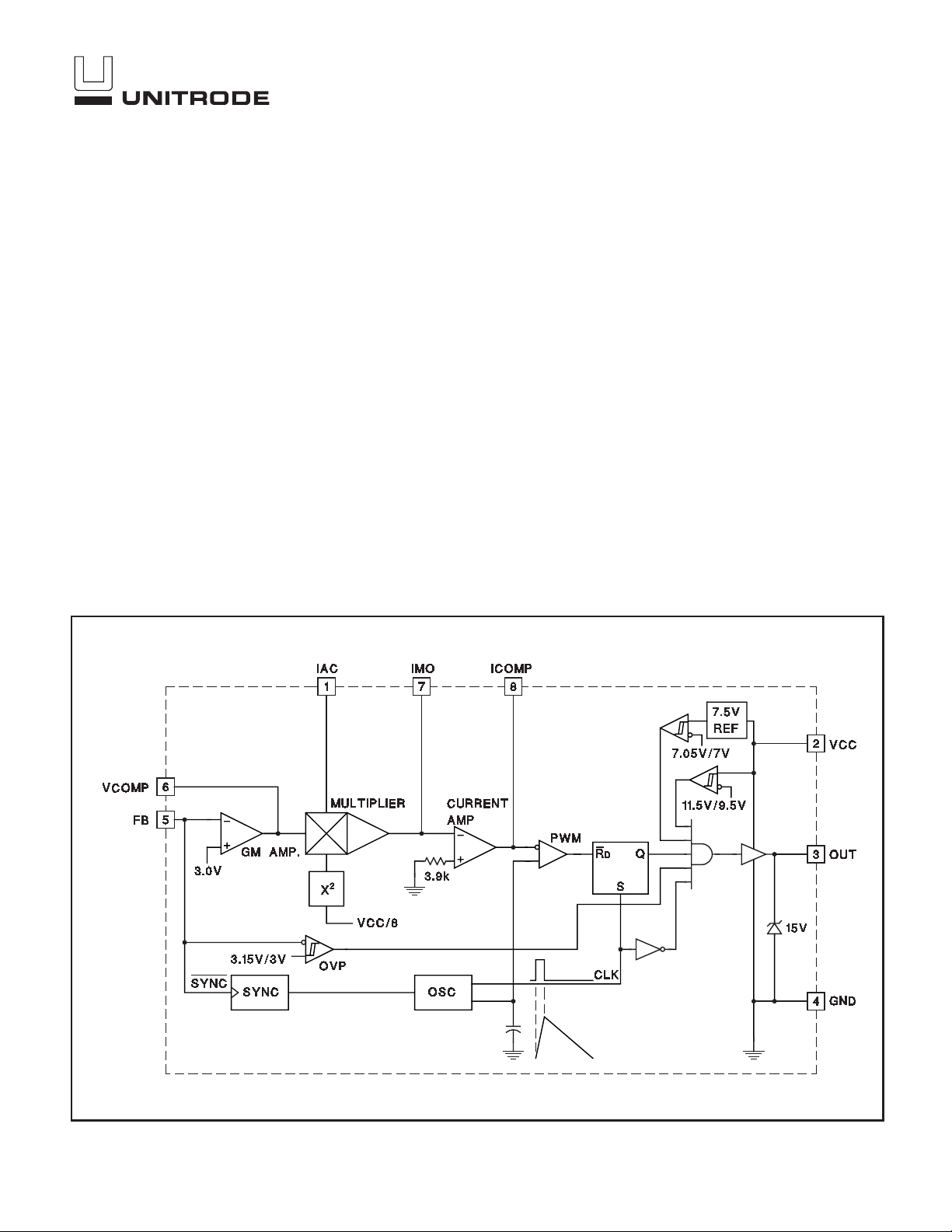
BLOCK DIAGRAM
DESCRIPTION
The UC3853 provides simple, yet high performance active power factor
correction. Using the same control technique as the UC1854, this 8-pin device exploits a simplified architecture and an internal oscillator to minimize
external component count. The UC3853 incorporates a precision multiplier/squarer/divider circuit, voltage and current loop error amplifiers, and a
precision voltage reference to implement average current mode control
with RMS line voltage compensation. This control technique maintains constant loop gain with changes in input voltage, which minimizes input line
current distortion over the worldwide input voltage range.
The internal 75kHz oscillator includes an external clock input, allowing synchronization to downstream converters. Additionally, the device features an
overvoltage protection comparator, a clamped MOSFET gate driver which
self-biases low during undervoltage lockout, and low startup and supply
current.
These devices are available in 8-pin plastic and ceramic dual in-line (DIP)
packages, and 8-lead small outline (SOIC) packages. The UC1853 is
specified for operation from –55°C to +125°C, the UC2853 is specified for
operation from –25°C to +85°C, and the UC3853 is specified for operation
from 0°C to +70°C.
11/97
UDG-94120-1
UC1853
UC2853
UC3853
ABSOLUTE MAXIMUM RATINGS
Supply Voltage (VCC) .............................40V
Output Drive Current,
Continuous ................................0.125A
Peak .......................................0.5A
Output Minimum Voltage.........................–0.3V
IAC Maximum Input Current........................1mA
IMO Maximum Output Current .....................–2mA
IMO Minimum Voltage ...........................–0.3V
FB Maximum Input Voltage ..........................5V
VCOMP Maximum Voltage.........................6.2V
ICOMP Sourcing Current ....................Self-Limiting
ICOMP Sinking Current ..........................20mA
ICOMP Maximum Voltage .........................7.2V
Storage Temperature ...................–65°C to +150°C
Junction Temperature...................–55°C to +150°C
Lead Temperature (Soldering, 10 sec.).............+300°C
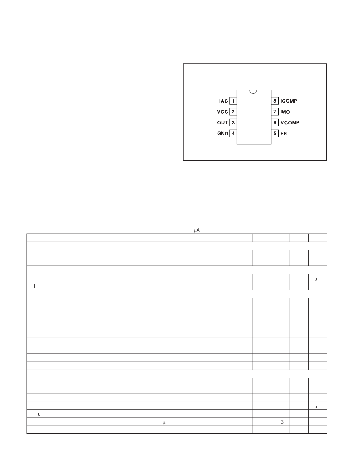
CONNECTION DIAGRAM
DIL-8, SOIC-8 (Top View)
JorN,DPackage
All voltages with respect to GND.Currents are positive into,
negative out of the specified terminal. Consult Packaging Section
of Databook for thermal limitations and considerations of
packages.
ELECTRICAL CHARACTERISTICS
PARAMETER TEST CONDITIONS MIN TYP MAX UNITS
Undervoltage Lockout Section
VCC Turn-on Threshold V
Hysteresis 1.5 1.8 2.1 V
Supply Current Section
CC Startup VCC = 8V, IAC = 100µA; VVCOMP,VICOMP Open 250 500
IV
IVCC IAC=0µA, VICOMP =0V 10 15 mA
Voltage Loop Error Amplifier Section
Transconductance IOUT=±20µA 0-70C 300 450 575 µmho
Input Voltage 0-70C 2.925 3 3.075 V
AVOL V
Output Sink Current V
Output Source Current VFB = 2.8V, VVCOMP = 3.75V –50 –20 µA
Output Voltage High 5.5 6 V
Output Voltage Low 0.6 0.9 V
Current Loop Error Amplifier Section
Offset Voltage 06mV
Voltage Gain V
Sink Current VIMO = 100mV, VICOMP =3V 1 mA
Source Current VIMO = –0.1V, VICOMP = 3V –150 –80
Output High I
Output Low IICOMP =50mA 0.3 0.8 V
PWM Modulator Gain VICOMP = 2V – 3V (Note 1) 20 %/V
Unless otherwise stated, these parameters apply for TA = –55°C to +125°C for the
UC1853; –25°C to +85°C for the 2853; and 0°C to +70°C for the UC3853; VCC =
16V, VFB = 3V, IAC = 100mA, VVCOMP = 3.75V, VICOMP = 3V, TA =TJ.
VCOMP,VICOMP Open 11.5 13 V
m
A
Temperature 135 640 µmho
Temperature 2.9 3.1 V
VCOMP =1V–4V 50 60 dB
FB = 3.2V, VVCOMP = 3.75V 20 50 µA
ICOMP =1V–4V 70 dB
m
A
ICOMP = –50mA 6 6.8 V
2

UC1853
UC2853
UC3853
ELECTRICAL CHARACTERISTICS
(continued)
PARAMETER TEST CONDITIONS MIN TYP MAX UNITS
Multiplier Section
Output Current – IAC Limited VCC = 11V, VVCOMP = 6V –230 –200 –170 µA
Output Current – Zero IAC = 0µA –2 –0.2 2 µA
Output Current – Power Limited VCC = 12V, V
Output Current VCC= 12V, V
Multiplier Gain Constant VCC= 12V, VVCOMP = 5.5V (Note 2) –1.05 –0.9 –0.75 V
Oscillator Section
Oscillator Initial Frequency TA = 25°C 67.5 75 82.5 kHz
Oscillator Frequency Line, Load, Temperature 56 75 94 kHz
Synchronization Frequency Range 100 kHz
Synchronization Pulse Amplitude Pulse slew rate = 100V/msec (Note 3) 2 V
Output Driver Section
Maximum Output Voltage 0mA load, VCC = 20V 12 15 17.5 V
Output High 0mA load, VCC = 12V, ref. to VCC –2.7 –1.7 V
Output Low (Device Inactive) Vcc = 0V, 20mA load (Sinking) 0.9 2.0 V
Output Low (Device Active) 50mA load (Sinking) 0.5 1 V
OUT Rise Time 1nF from OUT to GND 55 100 ns
OUT Fall Time 1nF from OUT to GND 35 100 ns
OUT Maximum Duty Cycle V
OVP Comparator Section
Threshold Voltage Volts Above EA Input V 90 150 mV
Hysteresis 80 mV
Unless otherwise stated, these parameters apply for TA = –55°C to +125°C for the
UC1853; –25°C to +85°C for the 2853; and 0°C to +70°C for the UC3853; VCC =
16V, VFB = 3V, IAC = 100mA, VVCOMP = 3.75V, VICOMP = 3V, TA =TJ.
VCOMP = 5.5V –236 –178 –168 µA
VCOMP = 2V –22 µA
VCC= 12V, VVCOMP = 5V –156 µA
VCC= 40V, VVCOMP =2V –2 µA
VCC= 40V, V
–50mA load, VCC = 12V, ref. to VCC –3 –2.2 V
ICOMP =0V 88 93 %
VCOMP = 5V –14 µA
–1
Note 1:
DutyCycle
PWM modulator gain
∆
=
ICOMP
V
∆
Note 2:
Gain constant K
()
=
•
IMO VCC
••
15
VCC
64
, VCC = 12V.
IAC VCOMP V
(.)
Note 3.
Synchronization is accomplished with a falling edge of 2V mag-
µ
nitude and 100V/
sec slew rate.
3

PIN DESCRIPTIONS
FB: Voltage Amplifier Inverting Input, Overvoltage
Comparator Input, Sync Input. This pin serves three
functions. FB accepts a fraction of the power factor
corrected output voltage through a voltage divider, and is
nominally regulated to 3V. FB voltages 5% greater than
nominal will trip the overvoltage comparator, and shut
down the output stage until the output voltage drops 5%.
The internal oscillator can be synchronized through FB by
injecting a 2V clock signal though a capacitor. To prevent
false tripping of the overvoltage comparator, the clock
signal must have a fast falling edge, but a slow rising
edge.See Application Note U-159 for more information.
GND: Ground. All voltages are measured with respect to
GND. The VCC bypass capacitor should be connected to
ground as close to the GND pin as possible.
IAC: AC Waveform Input. This input provides voltage
waveform information to the multiplier. The current loop
will try to produce a current waveform with the same
shape as the IAC signal. IAC is a low impedance input,
nominally at 2V, which accepts a current proportional to
the input voltage. Connect a resistor from the rectified input line to IAC which will conduct 500mA at maximum line
voltage.
IMO: Multiplier Output and Current Sense Inverting Input.
The output of the multiplier and the inverting input of the
current amplifier are connected together at IMO. Avoid
bringing this input below –0.5V to prevent the internal protection diode from conducting. The multiplier output is a
current, making this a summing node and allowing a differential current error amplifier configuration to reject
ground noise. The input resistance at this node should be
3.9k to minimize input bias current induced offset voltage.
See the Applications section for the recommended circuit
configuration.
OUT: Gate Driver Output.OUT provides high current gate
drive for the external power MOSFET. A 15V clamp pre-
UC1853
UC2853
UC3853
vents excessive MOSFET gate-to-source voltage so that
the UC3853 can be operated with VCC and high as 40V.
A series gate resistor of at least 5 ohms should be used
to minimize clamp voltage overshoot. In addition, a
Schottky diode such as a 1N5818 connected between
OUT and GND may be necessary to prevent parasitic
substrate diode conduction.
ICOMP: Current Loop Error Amplifier Output. The current loop error amplifier is a conventional operational
amplifier with a 150µA current source class A output
stage. Compensate the current loop by placing an impedance between ICOMP and IMO. This output can
swing above the oscillator peak voltage, allowing zero
duty cycle when necessary.
VCC: Input Supply Voltage. This pin serves two functions. It supplies power to the chip, and an input voltage
level signal to the squarer circuit. When this input is connected to a DC voltage proportional to the AC input RMS
voltage, the voltage loop gain is reduced by
.
2
CC
This configuration maintains constant loop gain. The
UC3853 input voltage range extends from 12V to 40V,
allowing an AC supply voltage range in excess of 85VAC
to 265VAC. Bypass VCC with at least a 0.1µF ceramic
capacitor to ensure proper operation. See the Applications section for the recommended circuit configuration.
VCOMP: Voltage Loop Error Amplifier Output. The
voltage loop error amplifier is a transconductance type
operational amplifier. A feedback impedance between
VCOMP and FB for loop compensation must be avoided
to maintain proper operation of the overvoltage
protection comparator. Instead, compensate the voltage
loop with an impedance between VCOMP and GND.
When VCOMP is below 1.5V, the multiplier output
current is zero.
4

UC3853 TYPICAL APPLICATION
UC1853
UC2853
UC3853
Note: the application circuit shownis a 100W, 75KHz design.
Additional application information can be found in Application
Note U–159 and Design Note DN–78.
UNITRODE CORPORATION
7 CONTINENTAL BLVD.• MERRIMACK, NH 03054
TEL. (603) 424-2410 • FAX (603) 424-3460
UDG-97127
5

IMPORTANT NOTICE
T exas Instruments and its subsidiaries (TI) reserve the right to make changes to their products or to discontinue
any product or service without notice, and advise customers to obtain the latest version of relevant information
to verify, before placing orders, that information being relied on is current and complete. All products are sold
subject to the terms and conditions of sale supplied at the time of order acknowledgement, including those
pertaining to warranty, patent infringement, and limitation of liability.
TI warrants performance of its semiconductor products to the specifications applicable at the time of sale in
accordance with TI’s standard warranty. Testing and other quality control techniques are utilized to the extent
TI deems necessary to support this warranty . Specific testing of all parameters of each device is not necessarily
performed, except those mandated by government requirements.
CERTAIN APPLICA TIONS USING SEMICONDUCT OR PRODUCTS MAY INVOLVE POTENTIAL RISKS OF
DEATH, PERSONAL INJURY, OR SEVERE PROPERTY OR ENVIRONMENTAL DAMAGE (“CRITICAL
APPLICATIONS”). TI SEMICONDUCTOR PRODUCTS ARE NOT DESIGNED, AUTHORIZED, OR
WARRANTED TO BE SUITABLE FOR USE IN LIFE-SUPPORT DEVICES OR SYSTEMS OR OTHER
CRITICAL APPLICA TIONS. INCLUSION OF TI PRODUCTS IN SUCH APPLICATIONS IS UNDERST OOD TO
BE FULLY AT THE CUSTOMER’S RISK.
In order to minimize risks associated with the customer’s applications, adequate design and operating
safeguards must be provided by the customer to minimize inherent or procedural hazards.
TI assumes no liability for applications assistance or customer product design. TI does not warrant or represent
that any license, either express or implied, is granted under any patent right, copyright, mask work right, or other
intellectual property right of TI covering or relating to any combination, machine, or process in which such
semiconductor products or services might be or are used. TI’s publication of information regarding any third
party’s products or services does not constitute TI’s approval, warranty or endorsement thereof.
Copyright 1999, Texas Instruments Incorporated
 Loading...