

UC1851
UC2851
UC3851
Programmable, Off-Line, PWM Controller
FEATURES
• All Control, Driving, Monitoring, and Protection
Functions Included
• Low-Current Off Line Start Circuit
• Voltage Feed Forward or Current Mode Control
• High Current Totem Pole Output
• 50% Absolute Max Duty Cycle
• PWM Latch for Single Pulse Per Period
• Pulse-by-Pulse Current Limiting plus Shutdown
for Over-Current Fau lt
• No Start-Up or Shutdown Transients
• Slow Turn-On Both Initially and After Fau lt
Shutdown
• Shutdown Upon Over or Under Voltage Sensing
• Latch Off or Continuous Retry After Fault
• 1% Reference Accuracy
• 500kHz Operation
• 18 Pin DIL or 20 Pin PLCC Package
DESCRIPTI ON
The UC1851 fami ly of PWM controllers are optimized for offline primary side control. These devices include a hi gh current
totem pole output stage and a toggle flip-flop for absolute 50%
duty cycle limiting. In all other respects this line of controllers is
pin for pin compatibl e with the UC1841 series. Inclusion of all
major housekee ping functions in these high performance controllers makes them ideal for use in cost sensitive applications.
Important features of these controllers include low current
start-up, linear feed-forward for constant volt-second operation,
and compatibility with both vol tage or curre nt mode control. In
addition, these devices include a programmable start threshold, as well as programmable over-voltage, under-voltage, and
over current fault threshol ds. The fault latch on these devices
can be configured for automatic restart, or latched off response
to a fault.
These devices are packaged in 18-pin plastic or ceramic dualin-line packages, or for surface mount applications, a 20 Pin
PLCC. The UC1851 is characterized for -55°C to +125°C op-
eration while the UC28 51 and UC3851 are designed for -40°C
to +85°C and 0°C to +70°C, respectively.
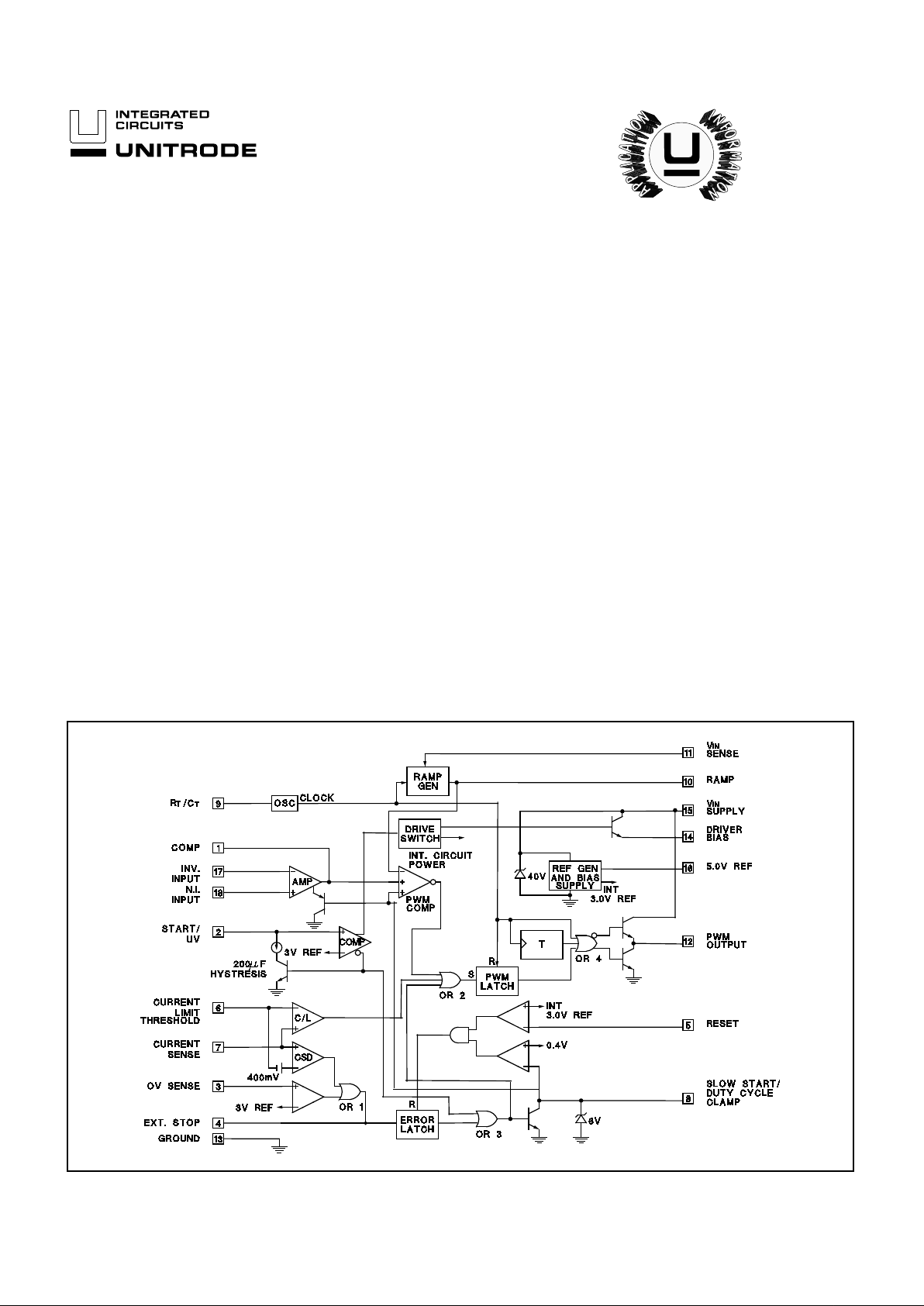
BLOCK DIAGRAM
10/94
UC1851
UC2851
UC3851
Supply Voltage, +V IN (Pin 15)
Voltage Driven. . . . . . . . . . . . . . . . . . . . . . . . . . . . . . . . +32V
Current Driven, 100 mA m aximum. . . . . . . . . . . Self-limiting
PWM Output Volta ge (Pin 12 ) . . . . . . . . . . . . . . . . . . . . . . . 40V
PWM Out put Current, Ste ady-State (Pin 12). . . . . . . . . 400mA
PWM Output Peak Energy Disc harge . . . . . . . . . . . . 20 µJo ules
Driver Bias Current (Pin 14). . . . . . . . . . . . . . . . . . . . . -200mA
Reference Output Current (Pin 16) . . . . . . . . . . . . . . . . -50mA
Slow-Start Sink Curren t (Pin 8) . . . . . . . . . . . . . . . . . . . . 20mA
V
IN Sense Current (Pin 11). . . . . . . . . . . . . . . . . . . . . . . . 10mA
Current Limit Input s (Pins 6 & 7) . . . . . . . . . . . . . -0.5 to +5. 5V
Stop Input (Pin 4) . . . . . . . . . . . . . . . . . . . . . . . . . -0.3 to +5.5V
Compara to r Inputs
(Pins 1–7, 9–11, 16). . . . . . . . . . . . . . Internal ly clamp ed at 12V
Power Dissipation at T
A
= 25°C (Note 3). . . . . . . . . . . 1000mW
Power Dissipation at T
C
= 25°C (Note 3). . . . . . . . . . . 2000mW
Operating Junct ion Te mp era tu re. . . . . . . . . . . -55°C to +150°C
Storage Temperature Ra nge. . . . . . . . . . . . . . -65°C to +150°C
Lead Temp era ture (Solder ing, 10 sec) . . . . . . . . . . . . . +300°C
Note 1:All voltages are with res pect to gro und, Pin 13.
Currents are positive-into, negative-out of the
specified terminal
Note 2:All pin number s are refer enc ed t o DIL-18 packa ge.
Note 3:Co nsult Packaging Sect ion of Dat abo ok for ther m al
limitations and cons id era tion s of packa ge.
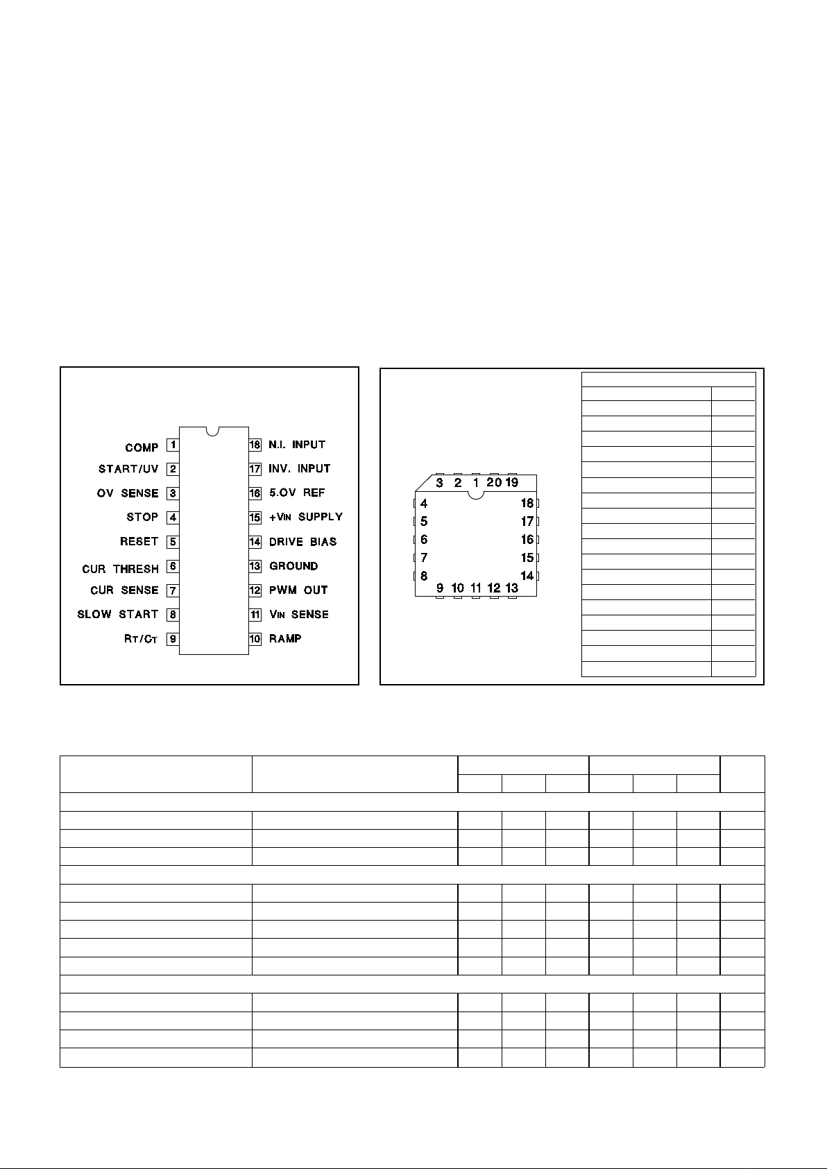
DIL-18, SOIC- 18 (T O P VIEW)
J or N, DW Package
CONNECTION DIAGRAMS
PACKAGE PIN FUNCTIONS
FUNCTION PIN
COMP 1
START/UV 2
OV SENSE 3
STOP 4
RESET 5
CUR THRESH 7
CUR SENSE 8
SLOW START 9
RT/CT 10
RAMP 11
VIN SENSE 12
PWM OUT 13
GROUND 14
DRIVE BIAS 15
+VIN SUPPLY 17
5.0V REF 18
INV. INPUT 19
N.I. INPUT 20
PLCC-20, LCC-20
(TOP VIEW)
Q, L PACKAGE
ABSOLUTE MAXI MUM RATING S (Note 1)
Unless otherw ise stat ed, these sp ecif icat io ns apply for TA = -55°C to +125°C for the
UC1851, -40°C to +85°C for the UC2851, and 0°C to 70°C for the UC3851; V
IN =
20V, R
T = 20kΩ, C T = .001 m fd , RR = 10kΩ, CR = .001mfd. Current Limit Threshold
= 200mV, T
A = TJ.
ELECTRICAL CHARACTERISTICS:
PARAMETER TEST CONDITIONS
UC1851 / UC2851 UC3851 UNITS
MIN TYP MAX MIN TYP MAX
Power Inputs
Start-Up Curr ent V
IN = 30V, Pin 2 = 2.5V 4.5 6 4.5 6 mA
Operating Cur ren t V
IN = 30V, Pin 2 = 3.5V 15 21 15 21 mA
Supply OV Clamp V
IN
= 20mA 333945333945V
Reference Sec tio n
Reference Voltage T
J = 25°C 4.95 5.0 5.05 4.9 5.0 5.1 V
Line Regulation V
IN
= 8 to 30V 10 15 10 20 mV
Load Regulation I
L = 0 to 10mA 1020 1030mV
Total Ref Variatio n Over Operating Temper at ure Range 4.9 5.1 4.85 5.15 V
Short Circuit Current V
REF = 0, TJ = 25°C -80 -100 -80 -100 mA
Oscillator
Nominal Frequency T
J = 25°C 47 50 53 45 50 55 kHz
Voltage Stability VIN = 8 to 30V 0.5 1 0.5 1 %
Total Ref Variatio n Over Operating Temper at ure Range 45 55 43 57 kH z
Maximum Frequency
R
T = 2kΩ, CT = 330pF
500 500 kHz
2
ELECTRICAL CHARACTERISTICS:
PARAMETER TEST CONDITIONS UC1851 / UC2851 UC3851 UNITS
MIN TYP MAX MIN TYP MAX
Ramp Ge nerator
Ramp Curren t, M in imum
I
SENSE = −10µA
-11 -14 -11 -14 µA
Ramp Current, Maximum I
SENSE = 1.0mA -0.9 -.95 -0.9 -.95 mA
Ramp Valley 0.3 0.4 0.6 0.3 0.4 0.6 V
Ramp Peak Clamping Level 3.9 4.2 4.5 3.9 4.2 4.5 V
Error Amplifier
Input Offs et Vo lta g e V
CM = 5.0V 0.5 5 2 10 m V
Input Bias Cur ren t 0.5 2 1 5 µA
Input Offs et Cu rr ent 0.5 0.5 µA
Open Loop Gain
∆V
O = 1 to 3V
60 66 60 66 dB
Output Swing (Max Ou tp ut ≤
Ramp Peak - 100mV)
Minimum Total Range 0.3 3.5 0.3 3.5 V
CMRR V
CM = 1.5 to 5.5V 70 80 70 80 dB
PSRR V
IN = 8 to 30V 70 80 70 80 dB
Short Circuit Current V
COMP = 0V -4 -10 -4 -10 mA
Gain Bandwidth (Not e 1) T
J = 25°C, AVOL = 0dB 1 2 1 2 MHz
Slew Rate (Note 1) T
J = 25°C, AVCL = 0dB 0.8 0.8 V/µs
PWM Section
Continuous Duty Cycle Range
(other than zero) (Note 1)
Minimum Total Cont inuou s Range
Ramp Peak < 4.2V
246246%
Output High Leve l I
SOURCE = 20mA 18 18.5 18 18. 5 V
I
SOURCE = 200mA 17 18.5 17 18.5 V
Rise Time (Note 1) T
J = 25°C, CL = 1nF 50 150 50 150 ns
Fall Time (Note 1) T
J = 25°C, CL = 1nF 50 150 50 150 ns
Output Saturation I
OUT = 20mA 0.2 0.4 0.2 0.4 V
I
OUT = 200mA 1.7 2.2 1.7 2.2 V
Comparator Delay (Note 1)
Pin 8 to Pin 12, T
J = 25°C, RL = 1kΩ
300 500 300 500 ns
Sequencing Functions
Comparator Thre sholds P ins 2, 3, 5 2.8 3.0 3.2 2.8 3.0 3.2 V
Input Bias Curren t Pins 3, 5 = 0V -1.0 -4.0 -1.0 -4.0 µA
Input Leakage Pins 3, 5 = 10V 0.1 2.0 0.1 2.0 µA
Start/UV Hyster esis Cur ren t Pin 2 = 2.5V 170 200 220 17 0 200 2 30 µA
Ext. Stop Threshold Pin 4 0.8 1.6 2.4 0.8 1.6 2.4 V
Error Latch Activat e Cur ren t Pin 4 = 0V, Pin 3 > 3V -120 -200 -120 -200 µA
Driver Bias Saturation Volta ge,
V
IN-VOH
IB = -50mA 2 3 2 3 V
Driver Bias Leakage V
B = 0V -0.1 -10 -0.1 -10 µA
Slow-Start Saturation I
S = 10mA 0.2 0.5 0.2 0.5 V
Slow-Start Leakage V
S = 4.5V 0.1 2.0 0.1 2.0 µA
Current Control
Current Limit Off set 0 5 0 10 mV
Current Shutdown O ffs et 370 400 430 360 400 440 mV
Input Bias Current Pin 7 = 0V -2 -5 -2 -5 µA
Common Mode Ran ge (No te 1) -0.4 3.0 -0.4 3.0 V
Current Limit Delay (Note 1) T
J = 25°C, Pin 7 to 12, RL = 1k 200 400 200 400 ns
Note 1:Guaranteed by d esign. Not 100% test ed in production.
UC1851
UC2851
UC3851
Unless otherw ise stat ed, these sp ecif icat io ns apply for TA = -55°C to +125°C for the
UC1851, -40°C to +85°C for the UC2851, and 0°C to 70°C for the UC3851; VIN =
20V, RT = 20 kΩ, CT = .0 01 mfd , R R = 10kΩ, CR = .001mfd. Current Limit Threshold
= 200mV, T A = TJ.
3

UC1851
UC2851
UC3851
PWM CONTROL
1. Oscillator Gener ates a fixed- frequ ency internal clock from an external R
T and CT.
Frequenc y =
K
C
RTCT
where KC is a f irst-orde r cor re ct ion factor ≈ 0.3 log (CT x 1012).
2. Ramp Gener ator:
Develops linear ramp with slope defined exter nally by
d
V
dT
=
sense voltage
R
RCR
.
C
R is normally selected ≤ CT and its value wi ll have some eff ect upon val ley dut y cycle .
Limiting th e minimum value for I
SENSE into pin 11 will establish a maximum dut y cycle clam p.
C
R terminal can be used as an input port for curre nt mode cont rol.
3. Error Amplifier Convention al oper at ional am p lifier for closed-loop gain and ph ase co mp ensa tion .
Low output impedance; unit y-gain stable.
The outpu t is held low by the slow start volta ge at tu rn on in order to minimiz e oversho ot .
4. Reference Ge n era tor: Precision 5.0V for inte rna l and exter nal usag e to 50mA.
Tracking 3.0V re fe ren ce f or inter nal usag e only with nom inal a ccur acy of ±2%.
40V clamp zener for chip OV protect ion, 100 mA maxim um curren t.
5. PWM Comparat or : Generates outpu t pulse which st arts at termina tion of clock pulse an d ends when t he ra mp input
crosses the lowes t of two posit ive input s.
6. PWM Latch: Terminates the PWM output pulse wh en set by inputs from either the PWM co mp arator, the
pulse-by- pulse co mparator, or the error latch. Reset s with each inter nal clock pulse.
7. PWM Output Switch: Totem pole out put stage capab le of sourc in g and sink ing 1 amp peak current . The active "on" stat e
is high.
SEQUENCING FUNCTIONS
1. Start/UV Sense: With an increasing voltage, this compar at or gener at es a turn -on signal and r elease s the slow st art
clamp at a start thresh old.
With a decreas ing volt age, it gener at es a turn -off comm and at a lower level separ at ed by a 200µA
hysteresis cur re nt .
2. Drive Switch: Disables most of the chip to hold interna l curr ent cons um ptio n low, and Driver Bias OFF, unt i l input
voltage reache s start thre shold.
3. Driver Bias: Supplies drive to external circuit ry upon star t -up .
4. Slow Start: Clamps low to hold PWM OFF. Upon rele ase, rise s with rat e contr o lled by R
SCS for slow increase of
output pulse width.
Can also be used as an alter nat e maxim um dut y cycle clamp with an ex terna l voltag e divider .
PROTECTION FUNCTIO NS
1. Error Latch: When set by moment ar y input , this latch insures immediat e PW M shutdown an d hold of f unt il reset.
Inputs to Error Latch are:
a. OV > 3.2V (Typically 3V)
b. Stop > 2.4V (Typically 1.6V)
c. Current Sense 40 0m V over thresh old. (Typic al).
Error Latch rese ts when slow st ar t voltag e falls to 0.4V if Res et Pin < 2.8V. W ith Pin 5 > 3.2V,
Error Latch will remain set.
2. Current Limiting: Different ial input comp ara to r terminat es indiv idual out put pulse s each time sense volt age r ises
above threshold.
When sense volt age r ises t o 400mV (t yp ical) abo ve t hre shold, a shutd own signa l is sent to Error
Latch.
3. External Stop : A volt ag e over 2.4 w ill set th e Error La tc h and ho ld the out put off.
A voltage less than 0. 8V will defeat the error latch and prevent shutd own.
A capacitor here will slow the actio n of the error latch for transien t protect ion by provid ing a Typical
Delay of 13ms/µF.
FUNCTIONAL DES CRIP TIO N
4

UC1851
UC2851
UC3851
Start/UV Hysteresis Current Output Saturation Characteristics
Oscillato r Frequen c y PWM Output Minimum Pulse Width
Error Amplifier O pen-Loo p Gain and Ph ase Shutdown Timing
5

UC1851
UC2851
UC3851
OPEN-LOOP CIRCUIT
High Peak currents a ssocia ted w ith capaci tive loads necessitate careful grounding techniques. Timing and bypass
capacitors should be connected close to pin 13 in a single ground point.
Programmable Soft Start and Restart Delay Circuit
For further application information see UC1840/UC1841
Data Sheets
UC1851 Power MOSFET Drive Inte rfac e
UNITRODE INTEGRATED CIRCUITS
7 CONTINENTAL BLVD. • MERRIMACK, NH 03054
TEL. (603) 424-2410 • FAX (603) 424-3460
Nominal Frequency =
1
RTCT
= 50kHz
Start Voltage = 3
R1
+ R2 + R3
R2 + R3
+0.2R1 = 12V
UV Fault Volt age
=
3
R1
+ R2 + R3
R2 + R3
= 8V
OV Fault V olt age
=
3
R1
+ R2 + R3
R3
=
32V
Current Limit = 200mV
Current Fault Volt age = 600mV
Duty Cycle Clamp = 50%
@V
IN = 15V, Duty Cycle = 48%
@V
IN = 30V, Duty Cycle = 24%
6

IMPORTANT NOTICE
T exas Instruments and its subsidiaries (TI) reserve the right to make changes to their products or to discontinue
any product or service without notice, and advise customers to obtain the latest version of relevant information
to verify, before placing orders, that information being relied on is current and complete. All products are sold
subject to the terms and conditions of sale supplied at the time of order acknowledgement, including those
pertaining to warranty, patent infringement, and limitation of liability.
TI warrants performance of its semiconductor products to the specifications applicable at the time of sale in
accordance with TI’s standard warranty. Testing and other quality control techniques are utilized to the extent
TI deems necessary to support this warranty. Specific testing of all parameters of each device is not necessarily
performed, except those mandated by government requirements.
CERT AIN APPLICATIONS USING SEMICONDUCTOR PRODUCTS MAY INVOLVE POTENTIAL RISKS OF
DEATH, PERSONAL INJURY, OR SEVERE PROPERTY OR ENVIRONMENTAL DAMAGE (“CRITICAL
APPLICATIONS”). TI SEMICONDUCTOR PRODUCTS ARE NOT DESIGNED, AUTHORIZED, OR
WARRANTED TO BE SUITABLE FOR USE IN LIFE-SUPPORT DEVICES OR SYSTEMS OR OTHER
CRITICAL APPLICATIONS. INCLUSION OF TI PRODUCTS IN SUCH APPLICA TIONS IS UNDERSTOOD T O
BE FULLY AT THE CUSTOMER’S RISK.
In order to minimize risks associated with the customer’s applications, adequate design and operating
safeguards must be provided by the customer to minimize inherent or procedural hazards.
TI assumes no liability for applications assistance or customer product design. TI does not warrant or represent
that any license, either express or implied, is granted under any patent right, copyright, mask work right, or other
intellectual property right of TI covering or relating to any combination, machine, or process in which such
semiconductor products or services might be or are used. TI’s publication of information regarding any third
party’s products or services does not constitute TI’s approval, warranty or endorsement thereof.
Copyright 1999, Texas Instruments Incorporated
 Loading...