

www.ti.com
11
A/B
V
cc
7 12
5 9
GROUND
4 7
RT/C
T
2 3
V
FB
1 1COMP
3 5
CURRENT
SENSE
34 V
2.50 V
OSC
UVLO
S/R
5 V
REF
VREF
Good
Logic
Internal
BIAS
Error
Amp
2R
R
1 V
CURRENT
SENSE
COMPARATOR
PWM
LATCH
S
R
T
8 14
V
REF
5 V
50 mA
7
V
C
106
OUTPUT
85
POWER
GROUND
Note 1:
Note 2:
A = DIL−8 Pin Number. B = SO−14 and CFP−14 Pin Number.
Toggle flip flop used only in 1844 and 1845.
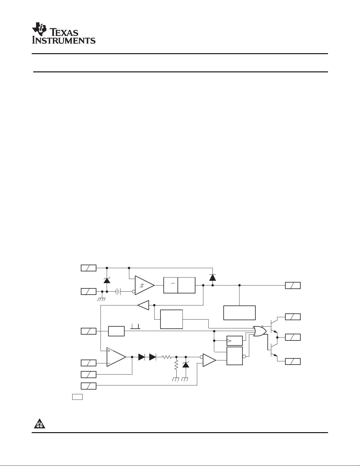
CURRENT MODE PWM CONTROLLER
FEATURES DESCRIPTION
• Optimized For Off-line and DC-to-DC
Converters
• Low Start-Up Current (<1 mA)
• Automatic Feed Forward Compensation
• Pulse-by-Pulse Current Limiting
• Enhanced Load Response Characteristics
• Under-Voltage Lockout With Hysteresis
• Double Pulse Suppression
• High Current Totem Pole Output
• Internally Trimmed Bandgap Reference
• 500-kHz Operation
• Low R
Error Amp
O
UC1842/3/4/5
UC2842/3/4/5
UC3842/3/4/5
SLUS223C – APRIL 1997 – REVISED JUNE 2007
The UC1842/3/4/5 family of control devices provides
the necessary features to implement off-line or
dc-to-dc fixed frequency current mode control
schemes with a minimal external parts count.
Internally implemented circuits include under-voltage
lockout featuring start up current less than 1 mA, a
precision reference trimmed for accuracy at the error
amp input, logic to insure latched operation, a PWM
comparator which also provides current limit control,
and a totem pole output stage designed to source or
sink high peak current. The output stage, suitable for
driving N-Channel MOSFETs, is low in the off state.
Differences between members of this family are the
under-voltage lockout thresholds and maximum duty
cycle ranges. The UC1842 and UC1844 have UVLO
thresholds of 16 V
off-line applications. The corresponding thresholds
for the UC1843 and UC1845 are 8.4 V and 7.6 V.
The UC1842 and UC1843 can operate to duty cycles
approaching 100%. A range of zero to 50% is
obtained by the UC1844 and UC1845 by the addition
of an internal toggle flip flop which blanks the output
off every other clock cycle.
ON
and 10 V
, ideally suited to
OFF
PRODUCTION DATA information is current as of publication date.
Products conform to specifications per the terms of the Texas
Instruments standard warranty. Production processing does not
necessarily include testing of all parameters.
Please be aware that an important notice concerning availability, standard warranty, and use in critical applications of Texas
Instruments semiconductor products and disclaimers thereto appears at the end of this data sheet.
BLOCK DIAGRAM
Copyright © 1997–2007, Texas Instruments Incorporated
www.ti.com
1
2
3
4
8
7
6
5
COMP
V
FB
I
SENSE
RT/C
T
V
REF
V
CC
OUTPUT
GROUND
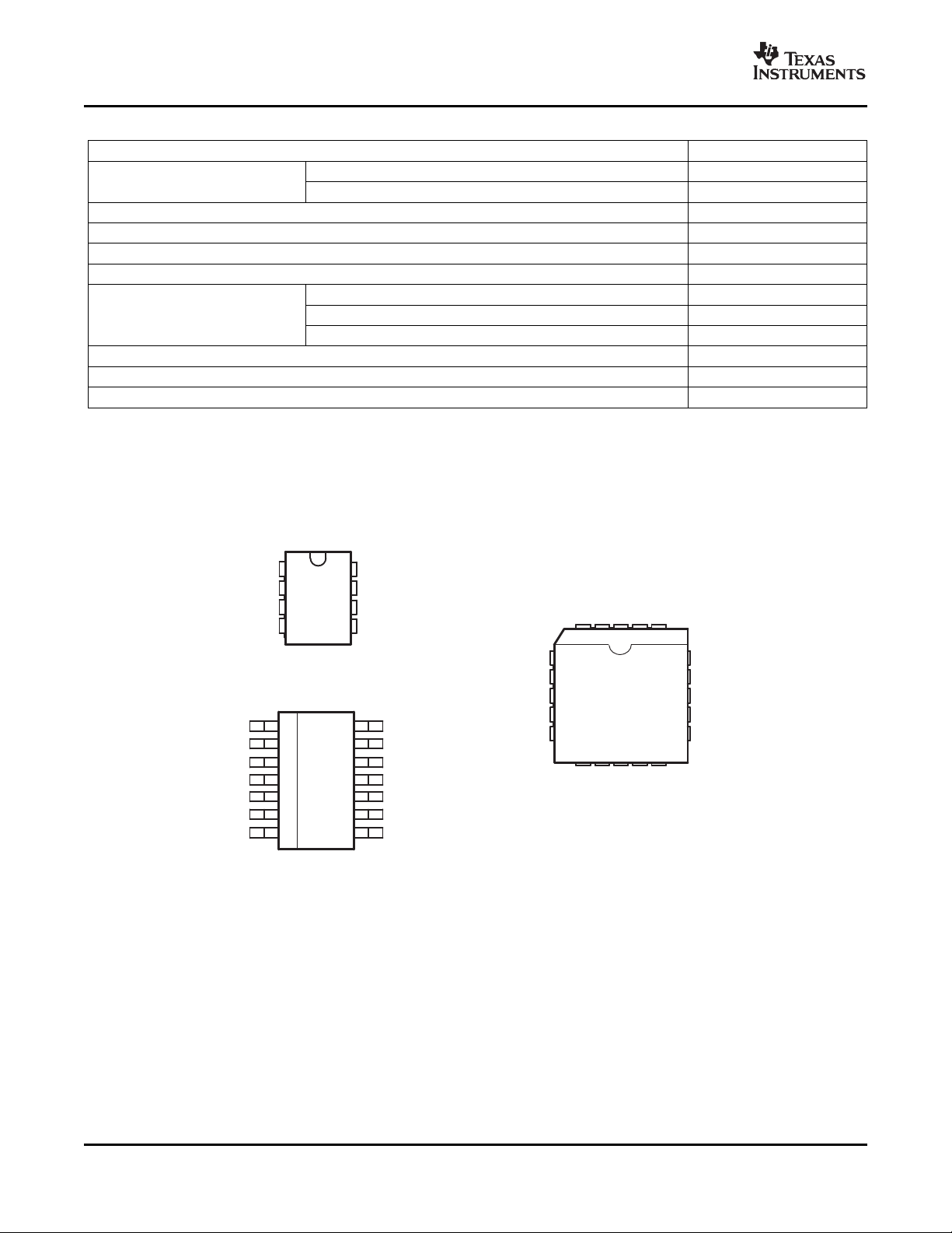
DIL-8, SOIC-8
N or J PACKAGE, D8 PACKAGE
(TOP VIEW)
NC − No internal connection
1
2
3
4
5
6
7
14
13
12
11
10
9
8
COMP
NC
V
FB
NC
I
SENSE
NC
RT/C
T
SOIC-14, CFP-14
D or W PACKAGE
(TOP VIEW)
V
REF
NC
V
CC
V
C
OUTPUT
GROUND
PWR GND
3 2 1 20 19
9 10 11 12 13
4
5
6
7
8
18
17
16
15
14
V
CC
V
C
NC
OUTPUT
NC
NC
V
FB
NC
I
SENSE
NC
PLCC-20
Q PACKAGE
(TOP VIEW)
NC
COMP
NC
PWR GND
GROUND
NC
NC
NC
R
T
/C
T
V
REF
UC1842/3/4/5
UC2842/3/4/5
UC3842/3/4/5
SLUS223C – APRIL 1997 – REVISED JUNE 2007
ABSOLUTE MAXIMUM RATINGS
Supply voltage
Output current ± 1 A
Output energy (capacitive load) 5 µ J
Analog inputs (Pins 2, 3) –0.3 V to 6.3 V
Error amp output sink current 10 mA
Power dissipation TA≤ 25 ° C (SOIC-14) 725 mW
Storage temperature range –65 ° C to 150 ° C
Junction temperature range –55 ° C to 150 ° C
Lead temperature (soldering, 10 seconds) 300 ° C
(1) All voltages are with respect to Pin 5. All currents are positive into the specified terminal. Consult Packaging Section of Databook for
thermal limitations and considerations of packages.
(1)
UNIT
Low impedance source 30 V
ICC< 30 mA Self Limiting
TA≤ 25 ° C (DIL-8) 1 W
TA≤ 25 ° C (SOIC-8) 650 mW
CONNECTION DIAGRAMS
2
Submit Documentation Feedback
www.ti.com
TempStability +
V
REF
(max)* VREF (min)
TJ(max)* TJ (min)
SLUS223C – APRIL 1997 – REVISED JUNE 2007
THERMAL CHARACTERISTICS
over operating free-air temperature range (unless otherwise noted)
PACKAGE θ
DIL-8 J 28
N 25 110
SOIC-8 D8 42 84-160
SOIC-14 D14 35 50-120
CFP-14 W 5.49 ° C/W 175.4C/W
PLCC-20 Q 34 43-75
(1) θJCdata values stated were derived from MIL-STD-1835B.
(2) Specified θJA(junction to ambient) is for devices mounted to 5 in2FR4 PC board with one ounce copper where noted. When resistance
range is given, lower values are for 5 in2. Test PWB was 0.062 in thick and typically used 0.635-mm trace widths for power packages
and 1.3-mm trace widths for non-power packages with 100 x 100-mil probe land area at the end of each trace.
JC
(1)
DISSIPATION RATINGS
PACKAGE
W 700 mW 5.5 mW/ ° C 452 mW 370 mW 150 mW
TA≤ 25 ° C DERATING FACTOR TA≤ 70 ° C TA≤ 85 ° CPO TA≤ 125 ° C
POWER RATING ABOVE TA≤ 25 ° C POWER RATING WER RATING POWER RATING
UC1842/3/4/5
UC2842/3/4/5
UC3842/3/4/5
θ
JA
125-160
(2)
(2)
(2)
(2)
ELECTRICAL CHARACTERISTICS
Unless otherwise stated, these specifications apply for –55 ° C ≤ TA≤ 125 ° C for the UC184X; –40 ° C ≤ TA≤ 85 ° C for the
UC284X; 0 ° C ≤ TA≤ 70 ° C for the 384X; V
PARAMETER TEST CONDITIONS UNIT
REFERENCE SECTION
Output Voltage TJ= 25 ° C, IO= 1 mA 4.95 5.00 5.05 4.90 5.00 5.10 V
Line Regulation 12 ≤ VIN≤ 25 V 6 20 6 20
Load Regulation 1 ≤ I0≤ 20 mA 6 25 6 25
Temp. Stability See
Total Output Variation Line, load, tempature
Output Noise Voltage 10 Hz ≤ f ≤ 10 kHz, TJ= 25 ° C
Long Term Stability TA= 125 ° C, 1000 Hrs
Output Short Circuit –30 –100 –180 –30 –100 –180 mA
OSCILLATOR SECTION
Initial Accuracy TJ= 25 ° C
Voltage Stability 12 ≤ VCC≤ 25 V 0.2% 1% 0.2% 1%
Temp. Stability T
Amplitude V
(1) Adjust V
(2) These parameters, although specified, are not 100% tested in production.
above the start threshold before setting at 15 V.
CC
(3) Temperature stability, sometimes referred to as average temperature coefficient, is described by the equation:
MIN
PIN
(2) (3)
≤ TA≤ T
4 peak-to-peak
CC
(4)
MAX
= 15 V
(2)
(1)
; RT= 10 k Ω ; CT= 3.3 nF, TA= TJ.
UC1842/3/4/5
UC2842/3/4/5
MIN TYP MAX MIN TYP MAX
(2)
(2)
(2)
4.9 5.1 4.82 5.18 V
47 52 57 47 52 57 kHz
(2)
UC3842/3/4/5
0.2 0.4 0.2 0.4 mV/ ° C
50 50 µ V
5 25 5 25 mV
5% 5%
1.7 1.7 V
mV
the appropriate temperature range. Note that the extremes in voltage do not necessarily occur at the extremes in temperature.
V
and V
REF(max)
are the maximum and minimum reference voltages measured over
REF(min)
(4) Output frequency equals oscillator frequency for the UC1842 and UC1843.
Output frequency is one half oscillator frequency for the UC1844 and UC1845.
Submit Documentation Feedback
3
www.ti.com
A +
DVPIN 1
DVPIN 3
, 0 v VPIN 3 v 0.8 V
UC1842/3/4/5
UC2842/3/4/5
UC3842/3/4/5
SLUS223C – APRIL 1997 – REVISED JUNE 2007
ELECTRICAL CHARACTERISTICS (continued)
Unless otherwise stated, these specifications apply for –55 ° C ≤ TA≤ 125 ° C for the UC184X; –40 ° C ≤ TA≤ 85 ° C for the
UC284X; 0 ° C ≤ TA≤ 70 ° C for the 384X; V
PARAMETER TEST CONDITIONS UNIT
ERROR AMP SECTION
Input Voltage V
Input Bias Current –0.3 –1 –0.3 –2 µ A
A
VOL
Unity Gain Bandwidth TJ= 25 ° C
PSRR 12 ≤ VCC≤ 25 V 60 70 60 70 dB
Output Sink Current V
Output Source Current V
V
High V
OUT
V
Low V
OUT
CURRENT SENSE SECTION
Gain See
Maximum Input Signal V
PSRR 12 ≤ VCC≤ 25 V
Input Bias Current –2 –10 –2 –10 µ A
Delay to Output V
OUTPUT SECTION
Output Low Level
Output High Level
Rise Time TJ= 25°C, CL= 1 nF
Fall Time TJ= 25 ° C, CL= 1nF
UNDER-VOLTAGE LOCKOUT SECTION
Start Threshold
Min. Operating Voltage After
Turn On
PWM SECTION
Maximum Duty Cycle
Minimum Duty Cycle 0% 0%
TOTAL STANDBY CURRENT
Start-Up Current 0.5 1 0.5 1
Operating Supply Current V
V
Zener Voltager ICC= 25 mA 30 34 30 34 V
CC
PIN 1
2 ≤ VO≤ 4 V 65 90 65 90 dB
PIN 2
PIN 2
PIN 2
PIN 2
(6) (7)
PIN 1
PIN 3
I
= 20 mA 0.1 0.4 0.1 0.4
SINK
I
= 200 mA 1.5 2.2 1.5 2.2
SINK
I
SOURCE
I
SOURCE
X842/4 15 16 17 14.5 16 17.5
X843/5 7.8 8.4 9.0 7.8 8.4 9.0
X842/4 9 10 11 8.5 10 11.5
X843/5 7.0 7.6 8.2 7.0 7.6 8.2
X842/3 95% 97% 100% 95% 97% 100%
X844/5 46% 48% 50% 47% 48% 50%
PIN 2
= 15 V ; RT= 10 k Ω ; CT= 3.3 nF, TA= TJ.
CC
UC1842/3/4/5
UC2842/3/4/5
UC3842/3/4/5
MIN TYP MAX MIN TYP MAX
= 2.5 V 2.45 2.50 2.55 2.42 2.50 2.58 V
(5)
= 2.7 V, V
= 2.3 V, V
= 1.1 V 2 6 2 6
PIN 1
= 5 V –0.5 –0.8 –0.5 –0.8
PIN 1
0.7 1 0.7 1 MHz
= 2.3 V, RL= 15 k Ω to ground 5 6 5 6
= 2.7 V, RL= 15 k Ω to Pin 8 0.7 1.1 0.7 1.1
2.85 3 3.15 2.85 3 3.15 V/V
(6)
= 5 V
= 0 V to 2 V
(5) (6)
(5)
0.9 1 1.1 0.9 1 1.1 V
70 70 dB
150 300 150 300 ns
= 20 mA 13 13.5 13 13.5
= 200 mA 12 13.5 12 13.5
(5)
(5)
= V
= 0 V 11 17 11 17
PIN 3
50 150 50 150
50 150 50 150
mA
V
V
ns
V
mA
(5) These parameters, although specified, are not 100% tested in production.
(6) Parameter measured at trip point of latch with V
(7) Gain defined as:
4
= 0.
PIN 2
Submit Documentation Feedback
www.ti.com
_
+
2.5 V
2
1
V
FB
COMP
Z
F
Z
I
0.5 mA
V
CC
<17 mA
<1 mA
V
OFF
V
ON
V
CC
7
V
CC
ON/OFF Command
to REST of IC
UC1842
UC1844
UC1843
UC1845
V
ON
V
OFF
16 V
10 V
8.4 V
7.6 V
Peak Current (IS) is Determined By The Formula
ERROR
AMP
2R
R
1 V
5
COMP
CURRENT
SENSE
GND
I
S
R
C
R
S
CURRENT
SENSE
COMPARATOR
,1.0 V
RS
I
SMAX
1
3
5
UC1842/3/4/5
UC2842/3/4/5
UC3842/3/4/5
SLUS223C – APRIL 1997 – REVISED JUNE 2007
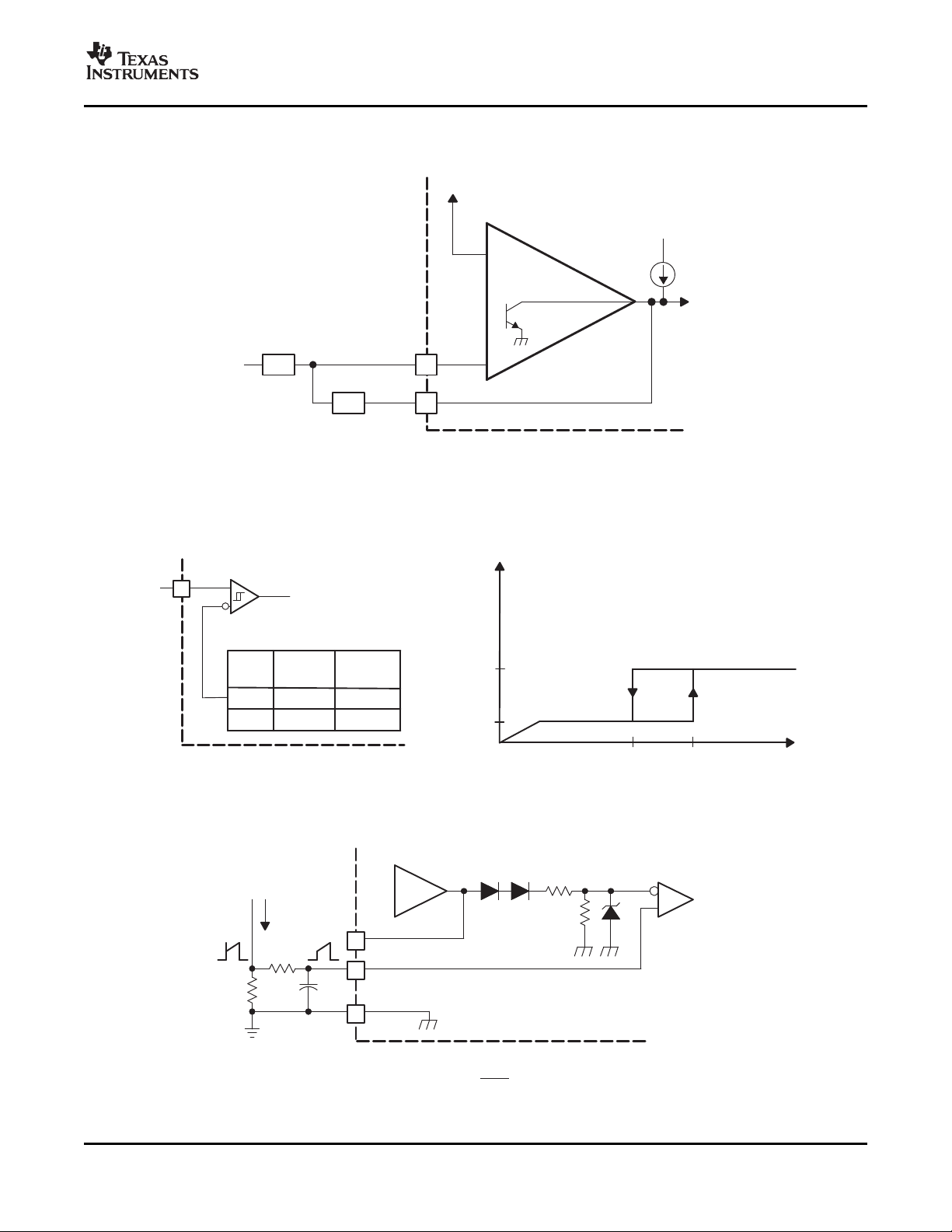
ERROR AMP CONFIGURATION
Error amp can source or sink up to 0.5 mA.
UNDER-VOLTAGE LOCKOUT
During under-voltage lock-out, the output drive is biased to sink minor amounts of current. Pin 6 should be
shunted to ground with a bleeder resistor to prevent activating the power switch with extraneous leakage
currents.
CURRENT SENSE CIRCUIT
A small RC filter may be required to suppress switch transients.
Submit Documentation Feedback
5
www.ti.com
8
4
5
V
REF
RT/C
T
GROUND
R
T
C
T
For RT> 5 K f
~
1.72
RTC
T
30
10
3
1
0.3
t
d
− ms
1 2.2 4.7 10 22 47 100
CT − nF
Deadtime vs CT (RT >5 kW)
R
T
− (k )W
100
30
10
3
100 1 k 10 k 100 k 1 M
f − Frequency − Hz
Timing Resistance vs Frequency
4
3
2
1
0
.01 .02 .03 .04 .05 .07 .1 .2 .3 .4 .5 .7 1
SINK SAT (VOL)
SOURCE SAT
(V
CC − VOH)
VCC = 15 V
TA = 25°C
TA = −55°C
Output Current, Source or Sink − A
Saturation Voltage − V
80
60
40
20
0
0
−45
−90
−135
−180
Voltage Gain − dB
Phase Margin − °
Av
θ
10 100 1 k 10 k 100 k 1 M 10 M
f − Frequency − Hz
UC1842/3/4/5
UC2842/3/4/5
UC3842/3/4/5
SLUS223C – APRIL 1997 – REVISED JUNE 2007
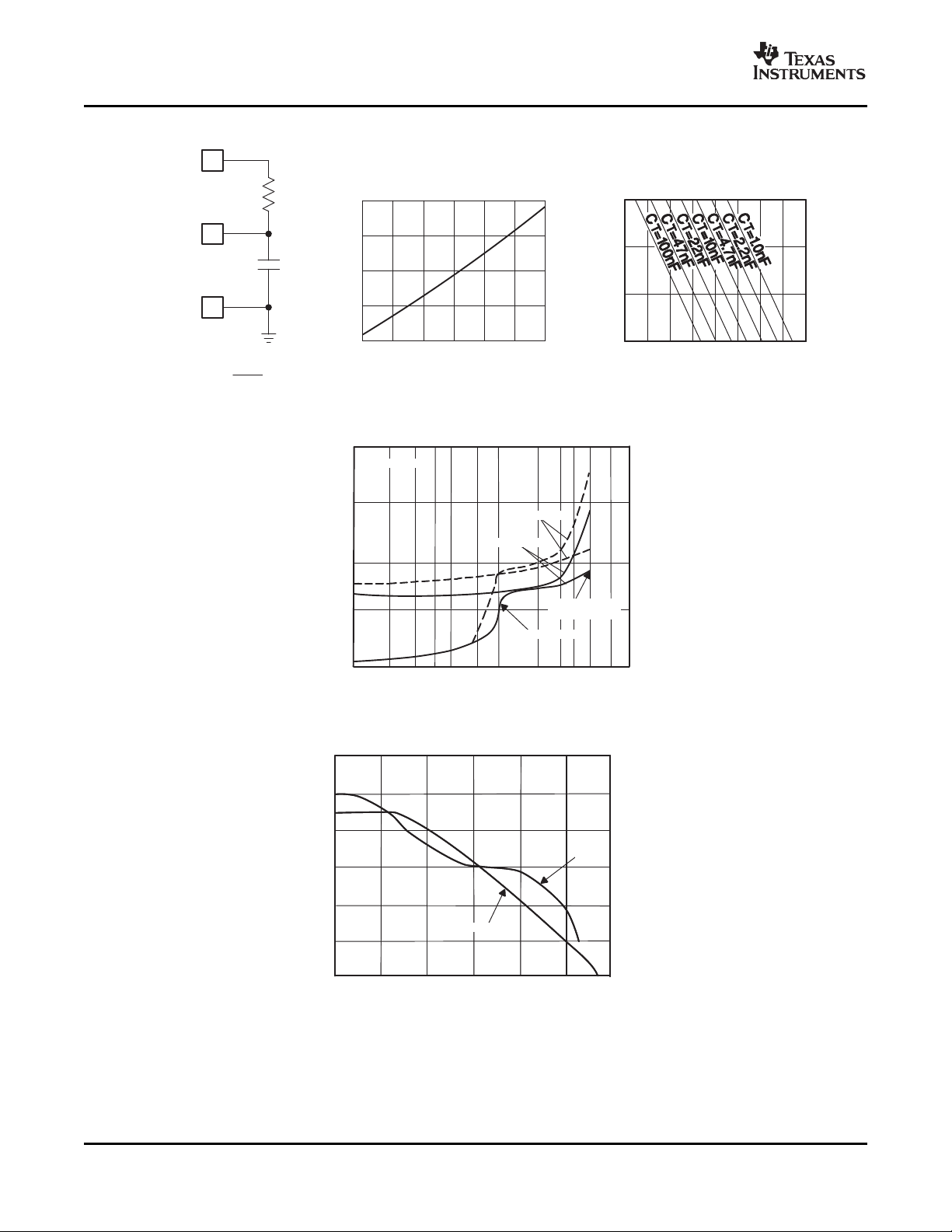
OSCILLATOR SECTION
OUTPUT SATURATION CHARACTERISTICS
ERROR AMPLIFIER OPEN-LOOP FREQUENCY RESPONSE
6
Submit Documentation Feedback
www.ti.com
4.7 kW
1 kW
ERROR AMP
ADJUST
4.7 kW
5 kW
I
SENSE
ADJUST
2N2222
100 kW
R1
1
2
3
4
8
7
6
5
COMP
UC1842
V
FB
I
SENSE
RT / C
T
C
T
0.1 mF
0.1 mF
A
1 kW
1 W
V
REF
V
CC
OUTPUT
GROUND
V
REF
V
CC
OUTPUT
GROUND
8
3
1 kW
330 W
SHUTDOWN
500 W
To Current
SENSE RESISTOR
V
REF
I
SENSE
1
SHUTDOWN
COMP
UC1842/3/4/5
UC2842/3/4/5
UC3842/3/4/5
SLUS223C – APRIL 1997 – REVISED JUNE 2007
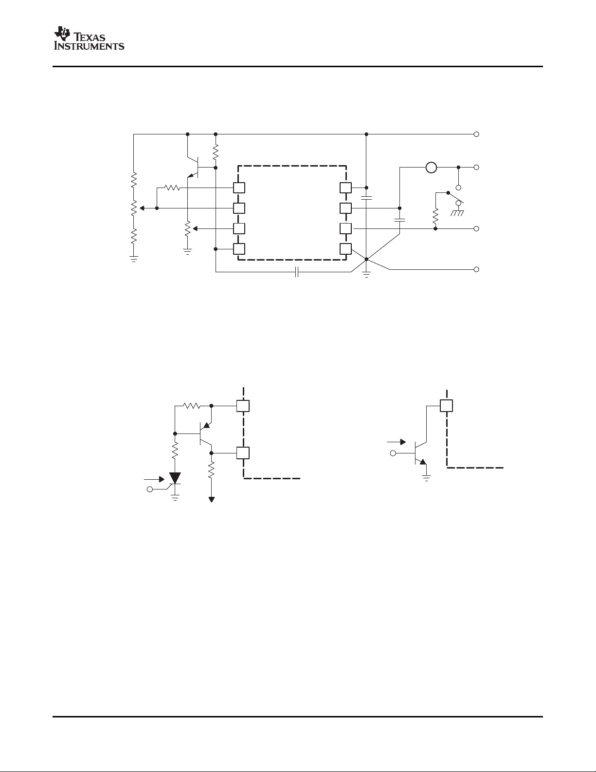
OPEN-LOOP LABORATORY FIXTURE
High peak currents associated with capacitive loads necessitate careful grounding techniques. Timing and bypas
capacitors should be conected close to pin 5 in a single point ground. The transistor and 5k potentiometer are
used to sample the oscillator waveform and apply an adjustable ramp to pin 3.
SHUTDOWN TECHNIQUES
Shutdown of the UC1842 can be accomplished by two methods; either raise pin 3 above 1 V or pull pin 1 below
a voltage two diode drops above ground. Either method causses the output of the PWM comparator to be high
(refer to block diagram). The PWM latch is reset dominant so that the output will remain low until the next clock
cycle after the shutdown condition at pin 1 and/or 3 is removed. In one example, an externally latched shutdown
may be accomplished by adding an SCR which will be reset by cycling V
this pint the reference turns off, allowing the SCR to reset.
below the lower UVLO threshold. At
CC
Submit Documentation Feedback
7
www.ti.com
R1
5 Ω 1 W
117 VAC
VARO
VM 68
C1
250 µF
250 V
R2
56 kΩ
2 W
R12
4.7 kΩ
2 W
C9
3300 pF
600 V
N
P
D4
1N3613
D2
1N3612
D3
1N3612
NC
R3
20 kΩ
R4
4.7 kΩ
C4
47 µF
25 V
R9
68 Ω
3 W
C3
22 µF
C2
100 µF
25 V
7
2
1
8
4
5
3
6
UC3844
R5 150 kΩ
C14
100 pF
R6
10 kΩ
C5
0.01 µF
C6
0.0022 µF
USD1120
R7
22 Ω
R8
1 kΩ
C7
470 pF
R13
20 kΩ
R10
0.55 Ω
1 W
Q1
UFN833
T1 D6
U9D946
L1
N5
C10
4700 µF
10 V
C11
4700 µF
10 V
+6 V
COM
+12 V
±12 V COM
−12 V
D7
UF81002
N12
N12
C12
2200 µF
16 V
C13
2200 µF
16 V
D8
UES1002
C8
680 pF
600 V
D8
1N3613
R11
2.7 kΩ
2 W
8
4
3
V
REF
RT / C
T
I
SENSE
UC1842/3
0.1 mF
R
T
C
T
R1
R2
C
I
SENSE
R
SENSE
UC1842/3/4/5
UC2842/3/4/5
UC3842/3/4/5
SLUS223C – APRIL 1997 – REVISED JUNE 2007
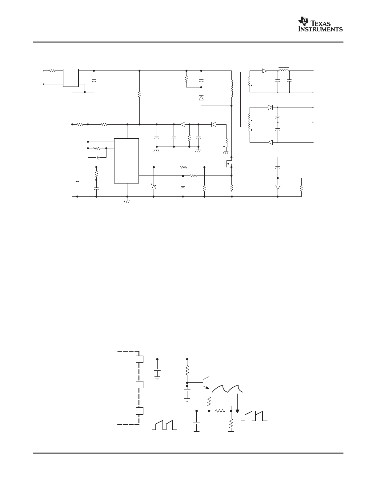
OFFLINE FLYBACK REGULATOR
Power Supply Specifications
1. Input Voltages
a. 5VAC to 130VA (50 Hz/60 Hz)
2. Line Isolation: 3750 V
3. Switchng Frequency: 40 kHz
4. Efficiency at Full Load 70%
5. Output Voltage:
a. +5 V, ± 5%; 1A to 4A load
Ripple voltage: 50 mV P-P Max
b. +12 V, ± 3%; 0.1A to 0.3A load
Ripple voltage: 100 mV P-P Max
c. –12 V, ± 3%; 0.1A to 0.3A load
Ripple voltage: 100 mV P-P Max
SLOPE COMPENSATION
A fraction of the oscillator ramp can be resistively summed with the current sense signal to provide slope
compensation for converters requiring duty cycles over 50%.
8
Submit Documentation Feedback

PACKAGE OPTION ADDENDUM
www.ti.com
PACKAGING INFORMATION
Orderable Device Status
5962-8670404DA ACTIVE CFP W 14 1 TBD A42 SNPB N / A for Pkg Type
5962-8670405PA ACTIVE CDIP JG 8 1 TBD A42 SNPB N / A for Pkg Type
5962-8670405VPA ACTIVE CDIP JG 8 1 TBD A42 N / A for Pkg Type
5962-8670405VXA ACTIVE LCCC FK 20 1 TBD POST-PLATE N / A for Pkg Type
5962-8670405XA ACTIVE LCCC FK 20 1 TBD POST-PLATE N / A for Pkg Type
5962-8670406PA ACTIVE CDIP JG 8 1 TBD A42 SNPB N / A for Pkg Type
5962-8670406VPA ACTIVE CDIP JG 8 1 TBD A42 N / A for Pkg Type
5962-8670406VXA ACTIVE LCCC FK 20 1 TBD POST-PLATE N / A for Pkg Type
5962-8670406XA ACTIVE LCCC FK 20 1 TBD POST-PLATE N / A for Pkg Type
5962-8670407PA ACTIVE CDIP JG 8 1 TBD A42 SNPB N / A for Pkg Type
5962-8670407VPA ACTIVE CDIP JG 8 1 TBD A42 N / A for Pkg Type
5962-8670407VXA ACTIVE LCCC FK 20 1 TBD POST-PLATE N / A for Pkg Type
5962-8670407XA ACTIVE LCCC FK 20 1 TBD POST-PLATE N / A for Pkg Type
5962-8670408PA ACTIVE CDIP JG 8 1 TBD A42 SNPB N / A for Pkg Type
5962-8670408VPA ACTIVE CDIP JG 8 1 TBD A42 N / A for Pkg Type
5962-8670408VXA ACTIVE LCCC FK 20 1 TBD POST-PLATE N / A for Pkg Type
5962-8670408XA ACTIVE LCCC FK 20 1 TBD POST-PLATE N / A for Pkg Type
UC1842AJ ACTIVE CDIP JG 8 1 TBD A42 SNPB N / A for Pkg Type
UC1842AJ883B ACTIVE CDIP JG 8 1 TBD A42 SNPB N / A for Pkg Type
UC1842AJQMLV ACTIVE CDIP JG 8 TBD Call TI Call TI
UC1842AL883B ACTIVE LCCC FK 20 1 TBD POST-PLATE N / A for Pkg Type
UC1842ALQMLV ACTIVE LCCC FK 20 TBD Call TI Call TI
UC1843AJ ACTIVE CDIP JG 8 1 TBD A42 SNPB N / A for Pkg Type
UC1843AJ883B ACTIVE CDIP JG 8 1 TBD A42 SNPB N / A for Pkg Type
UC1843AJQMLV ACTIVE CDIP JG 8 TBD Call TI Call TI
UC1843AL883B ACTIVE LCCC FK 20 1 TBD POST-PLATE N / A for Pkg Type
UC1843ALQMLV ACTIVE LCCC FK 20 TBD Call TI Call TI
UC1844AJ ACTIVE CDIP JG 8 1 TBD A42 SNPB N / A for Pkg Type
UC1844AJ883B ACTIVE CDIP JG 8 1 TBD A42 SNPB N / A for Pkg Type
UC1844AJQMLV ACTIVE CDIP JG 8 TBD Call TI Call TI
UC1844AL883B ACTIVE LCCC FK 20 1 TBD POST-PLATE N / A for Pkg Type
UC1844ALQMLV ACTIVE LCCC FK 20 TBD Call TI Call TI
UC1845AJ ACTIVE CDIP JG 8 1 TBD A42 SNPB N / A for Pkg Type
UC1845AJ883B ACTIVE CDIP JG 8 1 TBD A42 SNPB N / A for Pkg Type
UC1845AJQMLV ACTIVE CDIP JG 8 TBD Call TI Call TI
UC1845AL883B ACTIVE LCCC FK 20 1 TBD POST-PLATE N / A for Pkg Type
UC1845ALQMLV ACTIVE LCCC FK 20 TBD Call TI Call TI
UC1845W883B ACTIVE CFP W 14 1 TBD A42 SNPB N / A for Pkg Type
UC2842D ACTIVE SOIC D 14 50 Green (RoHS &
UC2842D8 ACTIVE SOIC D 8 75 Green (RoHS &
(1)
Package
Type
Package
Drawing
Pins Package
Qty
Eco Plan
no Sb/Br)
no Sb/Br)
(2)
Lead/Ball Finish MSL Peak Temp
CU NIPDAU Level-1-260C-UNLIM
CU NIPDAU Level-1-260C-UNLIM
27-Feb-2008
(3)
Addendum-Page 1

PACKAGE OPTION ADDENDUM
www.ti.com
Orderable Device Status
(1)
Package
Type
Package
Drawing
Pins Package
Qty
Eco Plan
UC2842D8G4 ACTIVE SOIC D 8 75 Green (RoHS &
(2)
Lead/Ball Finish MSL Peak Temp
CU NIPDAU Level-1-260C-UNLIM
no Sb/Br)
UC2842D8TR ACTIVE SOIC D 8 2500 Green (RoHS &
CU NIPDAU Level-1-260C-UNLIM
no Sb/Br)
UC2842D8TRG4 ACTIVE SOIC D 8 2500 Green (RoHS &
CU NIPDAU Level-1-260C-UNLIM
no Sb/Br)
UC2842DG4 ACTIVE SOIC D 14 50 Green (RoHS &
CU NIPDAU Level-1-260C-UNLIM
no Sb/Br)
UC2842DR ACTIVE SOIC D 14 TBD Call TI Call TI
UC2842DTR ACTIVE SOIC D 14 2500 Green (RoHS &
CU NIPDAU Level-1-260C-UNLIM
no Sb/Br)
UC2842DTRG4 ACTIVE SOIC D 14 2500 Green (RoHS &
CU NIPDAU Level-1-260C-UNLIM
no Sb/Br)
UC2842DW ACTIVE SOIC DW 16 40 Green (RoHS &
CU NIPDAU Level-2-260C-1 YEAR
no Sb/Br)
UC2842DWG4 ACTIVE SOIC DW 16 40 Green (RoHS &
CU NIPDAU Level-2-260C-1 YEAR
no Sb/Br)
UC2842DWTRG4 ACTIVE SOIC DW 16 TBD Call TI Call TI
UC2842J OBSOLETE CDIP JG 8 TBD Call TI Call TI
UC2842N ACTIVE PDIP P 8 50 Green (RoHS &
CU NIPDAU N / A for Pkg Type
no Sb/Br)
UC2842NG4 ACTIVE PDIP P 8 50 Green (RoHS &
CU NIPDAU N / A for Pkg Type
no Sb/Br)
UC2842P OBSOLETE PDIP P 8 TBD Call TI Call TI
UC2843D ACTIVE SOIC D 14 50 Green (RoHS &
CU NIPDAU Level-1-260C-UNLIM
no Sb/Br)
UC2843D8 ACTIVE SOIC D 8 75 Green (RoHS &
CU NIPDAU Level-1-260C-UNLIM
no Sb/Br)
UC2843D8G4 ACTIVE SOIC D 8 75 Green (RoHS &
CU NIPDAU Level-1-260C-UNLIM
no Sb/Br)
UC2843D8TR ACTIVE SOIC D 8 2500 Green (RoHS &
CU NIPDAU Level-1-260C-UNLIM
no Sb/Br)
UC2843D8TRG4 ACTIVE SOIC D 8 2500 Green (RoHS &
CU NIPDAU Level-1-260C-UNLIM
no Sb/Br)
UC2843DG4 ACTIVE SOIC D 14 50 Green (RoHS &
CU NIPDAU Level-1-260C-UNLIM
no Sb/Br)
UC2843DR OBSOLETE SOIC D 14 TBD Call TI Call TI
UC2843DTR ACTIVE SOIC D 14 2500 Green (RoHS &
CU NIPDAU Level-1-260C-UNLIM
no Sb/Br)
UC2843DTRG4 ACTIVE SOIC D 14 2500 Green (RoHS &
CU NIPDAU Level-1-260C-UNLIM
no Sb/Br)
UC2843J OBSOLETE CDIP JG 8 TBD Call TI Call TI
UC2843N ACTIVE PDIP P 8 50 Green (RoHS &
CU NIPDAU N / A for Pkg Type
no Sb/Br)
UC2843NG4 ACTIVE PDIP P 8 50 Green (RoHS &
CU NIPDAU N / A for Pkg Type
no Sb/Br)
UC2844D ACTIVE SOIC D 14 50 Green (RoHS &
CU NIPDAU Level-1-260C-UNLIM
no Sb/Br)
UC2844D8 ACTIVE SOIC D 8 75 Green (RoHS &
CU NIPDAU Level-1-260C-UNLIM
no Sb/Br)
27-Feb-2008
(3)
Addendum-Page 2

PACKAGE OPTION ADDENDUM
www.ti.com
Orderable Device Status
(1)
Package
Type
Package
Drawing
Pins Package
Qty
Eco Plan
UC2844D8G4 ACTIVE SOIC D 8 75 Green (RoHS &
(2)
Lead/Ball Finish MSL Peak Temp
CU NIPDAU Level-1-260C-UNLIM
no Sb/Br)
UC2844D8TR ACTIVE SOIC D 8 2500 Green (RoHS &
CU NIPDAU Level-1-260C-UNLIM
no Sb/Br)
UC2844D8TRG4 ACTIVE SOIC D 8 2500 Green (RoHS &
CU NIPDAU Level-1-260C-UNLIM
no Sb/Br)
UC2844DG4 ACTIVE SOIC D 14 50 Green (RoHS &
CU NIPDAU Level-1-260C-UNLIM
no Sb/Br)
UC2844DTR ACTIVE SOIC D 14 2500 Green (RoHS &
CU NIPDAU Level-1-260C-UNLIM
no Sb/Br)
UC2844DTRG4 ACTIVE SOIC D 14 2500 Green (RoHS &
CU NIPDAU Level-1-260C-UNLIM
no Sb/Br)
UC2844N ACTIVE PDIP P 8 50 Green (RoHS &
CU NIPDAU N / A for Pkg Type
no Sb/Br)
UC2844NG4 ACTIVE PDIP P 8 50 Green (RoHS &
CU NIPDAU N / A for Pkg Type
no Sb/Br)
UC2845D ACTIVE SOIC D 14 50 Green (RoHS &
CU NIPDAU Level-1-260C-UNLIM
no Sb/Br)
UC2845D8 ACTIVE SOIC D 8 75 Green (RoHS &
CU NIPDAU Level-1-260C-UNLIM
no Sb/Br)
UC2845D8G4 ACTIVE SOIC D 8 75 Green (RoHS &
CU NIPDAU Level-1-260C-UNLIM
no Sb/Br)
UC2845D8TR ACTIVE SOIC D 8 2500 Green (RoHS &
CU NIPDAU Level-1-260C-UNLIM
no Sb/Br)
UC2845D8TRG4 ACTIVE SOIC D 8 2500 Green (RoHS &
CU NIPDAU Level-1-260C-UNLIM
no Sb/Br)
UC2845DG4 ACTIVE SOIC D 14 50 Green (RoHS &
CU NIPDAU Level-1-260C-UNLIM
no Sb/Br)
UC2845DTR ACTIVE SOIC D 14 2500 Green (RoHS &
CU NIPDAU Level-1-260C-UNLIM
no Sb/Br)
UC2845DTRG4 ACTIVE SOIC D 14 2500 Green (RoHS &
CU NIPDAU Level-1-260C-UNLIM
no Sb/Br)
UC2845J OBSOLETE CDIP JG 8 TBD Call TI Call TI
UC2845N ACTIVE PDIP P 8 50 Green (RoHS &
CU NIPDAU N / A for Pkg Type
no Sb/Br)
UC2845NG4 ACTIVE PDIP P 8 50 Green (RoHS &
CU NIPDAU N / A for Pkg Type
no Sb/Br)
UC3842D ACTIVE SOIC D 14 50 Green (RoHS &
CU NIPDAU Level-1-260C-UNLIM
no Sb/Br)
UC3842D8 ACTIVE SOIC D 8 75 Green (RoHS &
CU NIPDAU Level-1-260C-UNLIM
no Sb/Br)
UC3842D8G4 ACTIVE SOIC D 8 75 Green (RoHS &
CU NIPDAU Level-1-260C-UNLIM
no Sb/Br)
UC3842D8TR ACTIVE SOIC D 8 2500 Green (RoHS &
CU NIPDAU Level-1-260C-UNLIM
no Sb/Br)
UC3842D8TRG4 ACTIVE SOIC D 8 2500 Green (RoHS &
CU NIPDAU Level-1-260C-UNLIM
no Sb/Br)
UC3842DG4 ACTIVE SOIC D 14 50 Green (RoHS &
CU NIPDAU Level-1-260C-UNLIM
no Sb/Br)
UC3842DTR ACTIVE SOIC D 14 2500 Green (RoHS &
CU NIPDAU Level-1-260C-UNLIM
no Sb/Br)
27-Feb-2008
(3)
Addendum-Page 3

PACKAGE OPTION ADDENDUM
www.ti.com
Orderable Device Status
(1)
Package
Type
Package
Drawing
Pins Package
Qty
Eco Plan
UC3842DTRG4 ACTIVE SOIC D 14 2500 Green (RoHS &
(2)
Lead/Ball Finish MSL Peak Temp
CU NIPDAU Level-1-260C-UNLIM
no Sb/Br)
UC3842N ACTIVE PDIP P 8 50 Green (RoHS &
CU NIPDAU N / A for Pkg Type
no Sb/Br)
UC3842NG4 ACTIVE PDIP P 8 50 Green (RoHS &
CU NIPDAU N / A for Pkg Type
no Sb/Br)
UC3842P OBSOLETE PDIP P 8 TBD Call TI Call TI
UC3843D ACTIVE SOIC D 14 50 Green (RoHS &
CU NIPDAU Level-1-260C-UNLIM
no Sb/Br)
UC3843D8 ACTIVE SOIC D 8 75 Green (RoHS &
CU NIPDAU Level-1-260C-UNLIM
no Sb/Br)
UC3843D8G4 ACTIVE SOIC D 8 75 Green (RoHS &
CU NIPDAU Level-1-260C-UNLIM
no Sb/Br)
UC3843D8TR ACTIVE SOIC D 8 2500 Green (RoHS &
CU NIPDAU Level-1-260C-UNLIM
no Sb/Br)
UC3843D8TRG4 ACTIVE SOIC D 8 2500 Green (RoHS &
CU NIPDAU Level-1-260C-UNLIM
no Sb/Br)
UC3843DG4 ACTIVE SOIC D 14 50 Green (RoHS &
CU NIPDAU Level-1-260C-UNLIM
no Sb/Br)
UC3843DTR ACTIVE SOIC D 14 2500 Green (RoHS &
CU NIPDAU Level-1-260C-UNLIM
no Sb/Br)
UC3843DTRG4 ACTIVE SOIC D 14 2500 Green (RoHS &
CU NIPDAU Level-1-260C-UNLIM
no Sb/Br)
UC3843N ACTIVE PDIP P 8 50 Green (RoHS &
CU NIPDAU N / A for Pkg Type
no Sb/Br)
UC3843NG4 ACTIVE PDIP P 8 50 Green (RoHS &
CU NIPDAU N / A for Pkg Type
no Sb/Br)
UC3843P OBSOLETE PDIP P 8 TBD Call TI Call TI
UC3843QTR OBSOLETE PLCC FN 20 TBD Call TI Call TI
UC3844D ACTIVE SOIC D 14 50 Green (RoHS &
CU NIPDAU Level-1-260C-UNLIM
no Sb/Br)
UC3844D8 ACTIVE SOIC D 8 75 Green (RoHS &
CU NIPDAU Level-1-260C-UNLIM
no Sb/Br)
UC3844D8G4 ACTIVE SOIC D 8 75 Green (RoHS &
CU NIPDAU Level-1-260C-UNLIM
no Sb/Br)
UC3844D8TR ACTIVE SOIC D 8 2500 Green (RoHS &
CU NIPDAU Level-1-260C-UNLIM
no Sb/Br)
UC3844D8TRG4 ACTIVE SOIC D 8 2500 Green (RoHS &
CU NIPDAU Level-1-260C-UNLIM
no Sb/Br)
UC3844DG4 ACTIVE SOIC D 14 50 Green (RoHS &
CU NIPDAU Level-1-260C-UNLIM
no Sb/Br)
UC3844DTR ACTIVE SOIC D 14 2500 Green (RoHS &
CU NIPDAU Level-1-260C-UNLIM
no Sb/Br)
UC3844DTRG4 ACTIVE SOIC D 14 2500 Green (RoHS &
CU NIPDAU Level-1-260C-UNLIM
no Sb/Br)
UC3844N ACTIVE PDIP P 8 50 Green (RoHS &
CU NIPDAU N / A for Pkg Type
no Sb/Br)
UC3844NG4 ACTIVE PDIP P 8 50 Green (RoHS &
CU NIPDAU N / A for Pkg Type
no Sb/Br)
UC3844P OBSOLETE PDIP P 8 TBD Call TI Call TI
UC3845AJ ACTIVE CDIP JG 8 1 TBD A42 SNPB N / A for Pkg Type
27-Feb-2008
(3)
Addendum-Page 4

PACKAGE OPTION ADDENDUM
www.ti.com
Orderable Device Status
(1)
Package
Type
Package
Drawing
Pins Package
Qty
Eco Plan
UC3845D ACTIVE SOIC D 14 50 Green (RoHS &
(2)
Lead/Ball Finish MSL Peak Temp
CU NIPDAU Level-1-260C-UNLIM
27-Feb-2008
(3)
no Sb/Br)
UC3845D8 ACTIVE SOIC D 8 75 Green (RoHS &
CU NIPDAU Level-1-260C-UNLIM
no Sb/Br)
UC3845D8G4 ACTIVE SOIC D 8 75 Green (RoHS &
CU NIPDAU Level-1-260C-UNLIM
no Sb/Br)
UC3845D8TR ACTIVE SOIC D 8 2500 Green (RoHS &
CU NIPDAU Level-1-260C-UNLIM
no Sb/Br)
UC3845D8TRG4 ACTIVE SOIC D 8 2500 Green (RoHS &
CU NIPDAU Level-1-260C-UNLIM
no Sb/Br)
UC3845DG4 ACTIVE SOIC D 14 50 Green (RoHS &
CU NIPDAU Level-1-260C-UNLIM
no Sb/Br)
UC3845DTR ACTIVE SOIC D 14 2500 Green (RoHS &
CU NIPDAU Level-1-260C-UNLIM
no Sb/Br)
UC3845DTRG4 ACTIVE SOIC D 14 2500 Green (RoHS &
CU NIPDAU Level-1-260C-UNLIM
no Sb/Br)
UC3845N ACTIVE PDIP P 8 50 Green (RoHS &
CU NIPDAU N / A for Pkg Type
no Sb/Br)
UC3845NG4 ACTIVE PDIP P 8 50 Green (RoHS &
CU NIPDAU N / A for Pkg Type
no Sb/Br)
UC3845P OBSOLETE PDIP P 8 TBD Call TI Call TI
(1)
The marketing status values are defined as follows:
ACTIVE: Product device recommended for new designs.
LIFEBUY: TI has announced that the device will be discontinued, and a lifetime-buy period is in effect.
NRND: Not recommended for new designs. Device is in production to support existing customers, but TI does not recommend using this part in
a new design.
PREVIEW: Device has been announced but is not in production. Samples may or may not be available.
OBSOLETE: TI has discontinued the production of the device.
(2)
Eco Plan - The planned eco-friendly classification: Pb-Free (RoHS), Pb-Free (RoHS Exempt), or Green (RoHS & no Sb/Br) - please check
http://www.ti.com/productcontent for the latest availability information and additional product content details.
TBD: The Pb-Free/Green conversion plan has not been defined.
Pb-Free (RoHS): TI's terms "Lead-Free" or "Pb-Free" mean semiconductor products that are compatible with the current RoHS requirements
for all 6 substances, including the requirement that lead not exceed 0.1% by weight in homogeneous materials. Where designed to be soldered
at high temperatures, TI Pb-Free products are suitable for use in specified lead-free processes.
Pb-Free (RoHS Exempt): This component has a RoHS exemption for either 1) lead-based flip-chip solder bumps used between the die and
package, or 2) lead-based die adhesive used between the die and leadframe. The component is otherwise considered Pb-Free (RoHS
compatible) as defined above.
Green (RoHS & no Sb/Br): TI defines "Green" to mean Pb-Free (RoHS compatible), and free of Bromine (Br) and Antimony (Sb) based flame
retardants (Br or Sb do not exceed 0.1% by weight in homogeneous material)
(3)
MSL, Peak Temp. -- The Moisture Sensitivity Level rating according to the JEDEC industry standard classifications, and peak solder
temperature.
Important Information and Disclaimer:The information provided on this page represents TI's knowledge and belief as of the date that it is
provided. TI bases its knowledge and belief on information provided by third parties, and makes no representation or warranty as to the
accuracy of such information. Efforts are underway to better integrate information from third parties. TI has taken and continues to take
reasonable steps to provide representative and accurate information but may not have conducted destructive testing or chemical analysis on
incoming materials and chemicals. TI and TI suppliers consider certain information to be proprietary, and thus CAS numbers and other limited
information may not be available for release.
In no event shall TI's liability arising out of such information exceed the total purchase price of the TI part(s) at issue in this document sold by TI
to Customer on an annual basis.
Addendum-Page 5

PACKAGE MATERIALS INFORMATION
www.ti.com
TAPE AND REEL INFORMATION
19-Mar-2008
*All dimensions are nominal
Device Package
UC2842D8TR SOIC D 8 2500 330.0 12.4 6.4 5.2 2.1 8.0 12.0 Q1
UC2842DTR SOIC D 14 2500 330.0 16.4 6.5 9.0 2.1 8.0 16.0 Q1
UC2843D8TR SOIC D 8 2500 330.0 12.4 6.4 5.2 2.1 8.0 12.0 Q1
UC2843DTR SOIC D 14 2500 330.0 16.4 6.5 9.0 2.1 8.0 16.0 Q1
UC2844D8TR SOIC D 8 2500 330.0 12.4 6.4 5.2 2.1 8.0 12.0 Q1
UC2844DTR SOIC D 14 2500 330.0 16.4 6.5 9.0 2.1 8.0 16.0 Q1
UC2845D8TR SOIC D 8 2500 330.0 12.4 6.4 5.2 2.1 8.0 12.0 Q1
UC2845DTR SOIC D 14 2500 330.0 16.4 6.5 9.0 2.1 8.0 16.0 Q1
UC3842D8TR SOIC D 8 2500 330.0 12.4 6.4 5.2 2.1 8.0 12.0 Q1
UC3842DTR SOIC D 14 2500 330.0 16.4 6.5 9.0 2.1 8.0 16.0 Q1
UC3843D8TR SOIC D 8 2500 330.0 12.4 6.4 5.2 2.1 8.0 12.0 Q1
UC3843DTR SOIC D 14 2500 330.0 16.4 6.5 9.0 2.1 8.0 16.0 Q1
UC3844D8TR SOIC D 8 2500 330.0 12.4 6.4 5.2 2.1 8.0 12.0 Q1
UC3844DTR SOIC D 14 2500 330.0 16.4 6.5 9.0 2.1 8.0 16.0 Q1
UC3845D8TR SOIC D 8 2500 330.0 12.4 6.4 5.2 2.1 8.0 12.0 Q1
UC3845DTR SOIC D 14 2500 330.0 16.4 6.5 9.0 2.1 8.0 16.0 Q1
Type
Package
Drawing
Pins SPQ Reel
Diameter
(mm)
Reel
Width
W1 (mm)
A0 (mm) B0 (mm) K0 (mm) P1
(mm)W(mm)
Pin1
Quadrant
Pack Materials-Page 1

PACKAGE MATERIALS INFORMATION
www.ti.com
19-Mar-2008
*All dimensions are nominal
Device Package Type Package Drawing Pins SPQ Length (mm) Width (mm) Height (mm)
UC2842D8TR SOIC D 8 2500 340.5 338.1 20.6
UC2842DTR SOIC D 14 2500 333.2 345.9 28.6
UC2843D8TR SOIC D 8 2500 340.5 338.1 20.6
UC2843DTR SOIC D 14 2500 333.2 345.9 28.6
UC2844D8TR SOIC D 8 2500 340.5 338.1 20.6
UC2844DTR SOIC D 14 2500 333.2 345.9 28.6
UC2845D8TR SOIC D 8 2500 340.5 338.1 20.6
UC2845DTR SOIC D 14 2500 333.2 345.9 28.6
UC3842D8TR SOIC D 8 2500 340.5 338.1 20.6
UC3842DTR SOIC D 14 2500 333.2 345.9 28.6
UC3843D8TR SOIC D 8 2500 340.5 338.1 20.6
UC3843DTR SOIC D 14 2500 333.2 345.9 28.6
UC3844D8TR SOIC D 8 2500 340.5 338.1 20.6
UC3844DTR SOIC D 14 2500 333.2 345.9 28.6
UC3845D8TR SOIC D 8 2500 340.5 338.1 20.6
UC3845DTR SOIC D 14 2500 333.2 345.9 28.6
Pack Materials-Page 2


MECHANICAL DATA
MLCC006B – OCTOBER 1996
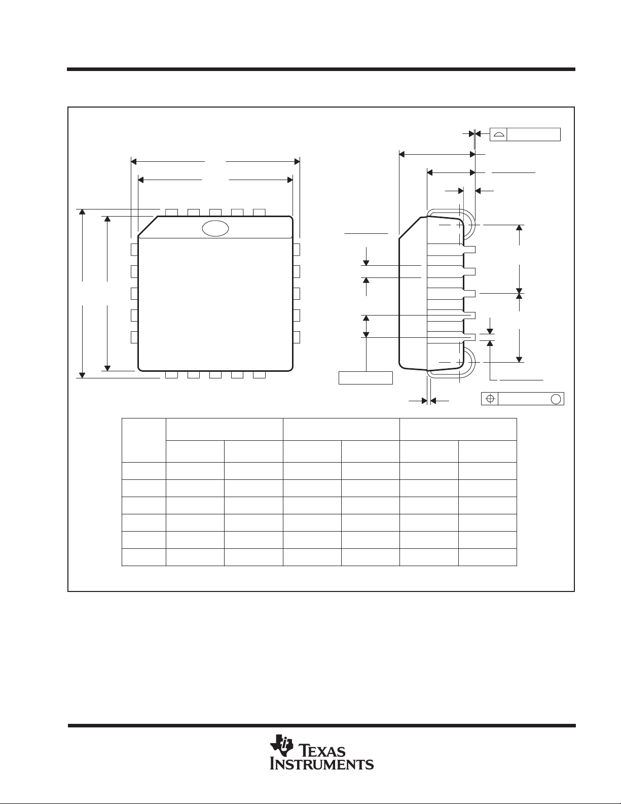
FK (S-CQCC-N**) LEADLESS CERAMIC CHIP CARRIER
28 TERMINAL SHOWN
A SQ
B SQ
19
20
21
22
23
24
25
12826 27
1314151618 17
0.020 (0,51)
0.010 (0,25)
12
MIN
0.342
(8,69)
0.442
0.640
0.739
0.938
1.141
A
0.358
(9,09)
0.458
(11,63)
0.660
(16,76)
0.761
(19,32)(18,78)
0.962
(24,43)
1.165
(29,59)
NO. OF
TERMINALS
**
11
10
9
8
7
6
5
432
20
28
44
52
68
84
0.020 (0,51)
0.010 (0,25)
(11,23)
(16,26)
(23,83)
(28,99)
MINMAX
0.307
(7,80)
0.406
(10,31)
0.495
(12,58)
0.495
(12,58)
0.850
(21,6)
1.047
(26,6)
0.080 (2,03)
0.064 (1,63)
B
MAX
0.358
(9,09)
0.458
(11,63)
0.560
(14,22)
0.560
(14,22)
0.858
(21,8)
1.063
(27,0)
0.055 (1,40)
0.045 (1,14)
0.028 (0,71)
0.022 (0,54)
0.050 (1,27)
NOTES: A. All linear dimensions are in inches (millimeters).
B. This drawing is subject to change without notice.
C. This package can be hermetically sealed with a metal lid.
D. The terminals are gold plated.
E. Falls within JEDEC MS-004
POST OFFICE BOX 655303 • DALLAS, TEXAS 75265
0.045 (1,14)
0.035 (0,89)
0.045 (1,14)
0.035 (0,89)
4040140/D 10/96


MECHANICAL DATA
MPLC004A – OCT OBER 1994
FN (S-PQCC-J**) PLASTIC J-LEADED CHIP CARRIER
20 PIN SHOWN
Seating Plane
0.004 (0,10)
D
D1
13
4
E1E
8
9
NO. OF
PINS
**
D/E
19
13
18
14
0.032 (0,81)
0.026 (0,66)
0.050 (1,27)
0.008 (0,20) NOM
D1/E1
MINMAXMIN
MAX
D2/E2
MIN
0.180 (4,57) MAX
0.120 (3,05)
0.090 (2,29)
0.020 (0,51) MIN
D2/E2
D2/E2
0.021 (0,53)
0.013 (0,33)
0.007 (0,18)
MAX
M
20
28
44
52
68
84
NOTES: A. All linear dimensions are in inches (millimeters).
B. This drawing is subject to change without notice.
C. Falls within JEDEC MS-018
0.385 (9,78)
0.485 (12,32)
0.685 (17,40)
0.785 (19,94)
0.985 (25,02)
1.185 (30,10)
0.395 (10,03)
0.495 (12,57)
0.695 (17,65)
0.795 (20,19)
0.995 (25,27)
1.195 (30,35)
0.350 (8,89)
0.450 (11,43)
0.650 (16,51)
0.750 (19,05)
0.950 (24,13)
1.150 (29,21)
0.356 (9,04)
0.456 (11,58)
0.656 (16,66)
0.756 (19,20)
0.958 (24,33)
1.158 (29,41)
0.141 (3,58)
0.191 (4,85)
0.291 (7,39)
0.341 (8,66)
0.441 (11,20)
0.541 (13,74)
0.169 (4,29)
0.219 (5,56)
0.319 (8,10)
0.369 (9,37)
0.469 (11,91)
0.569 (14,45)
4040005/B 03/95
POST OFFICE BOX 655303 • DALLAS, TEXAS 75265
1

MECHANICAL DATA
MPDI001A – JANUARY 1995 – REVISED JUNE 1999
P (R-PDIP-T8) PLASTIC DUAL-IN-LINE
0.400 (10,60)
0.355 (9,02)
8
5
0.260 (6,60)
0.240 (6,10)
1
0.021 (0,53)
0.015 (0,38)
NOTES: A. All linear dimensions are in inches (millimeters).
B. This drawing is subject to change without notice.
C. Falls within JEDEC MS-001
4
0.070 (1,78) MAX
0.020 (0,51) MIN
0.200 (5,08) MAX
0.125 (3,18) MIN
0.100 (2,54)
0.010 (0,25)
Seating Plane
M
0.325 (8,26)
0.300 (7,62)
0.015 (0,38)
Gage Plane
0.010 (0,25) NOM
0.430 (10,92)
MAX
4040082/D 05/98
For the latest package information, go to http://www.ti.com/sc/docs/package/pkg_info.htm
POST OFFICE BOX 655303 • DALLAS, TEXAS 75265


MECHANICAL DATA
MCER001A – JANUARY 1995 – REVISED JANUARY 1997
JG (R-GDIP-T8) CERAMIC DUAL-IN-LINE
0.400 (10,16)
0.355 (9,00)
0.063 (1,60)
0.015 (0,38)
0.100 (2,54)
8
1
5
4
0.065 (1,65)
0.045 (1,14)
0.020 (0,51) MIN
0.023 (0,58)
0.015 (0,38)
0.280 (7,11)
0.245 (6,22)
0.310 (7,87)
0.290 (7,37)
0.200 (5,08) MAX
Seating Plane
0.130 (3,30) MIN
0°–15°
0.014 (0,36)
0.008 (0,20)
NOTES: A. All linear dimensions are in inches (millimeters).
B. This drawing is subject to change without notice.
C. This package can be hermetically sealed with a ceramic lid using glass frit.
D. Index point is provided on cap for terminal identification.
E. Falls within MIL STD 1835 GDIP1-T8
4040107/C 08/96
POST OFFICE BOX 655303 • DALLAS, TEXAS 75265

IMPORTANT NOTICE
Texas Instruments Incorporated and its subsidiaries (TI) reserve the right to make corrections, modifications, enhancements, improvements,
and other changes to its products and services at any time and to discontinue any product or service without notice. Customers should
obtain the latest relevant information before placing orders and should verify that such information is current and complete. All products are
sold subject to TI’s terms and conditions of sale supplied at the time of order acknowledgment.
TI warrants performance of its hardware products to the specifications applicable at the time of sale in accordance with TI’s standard
warranty. Testing and other quality control techniques are used to the extent TI deems necessary to support this warranty. Except where
mandated by government requirements, testing of all parameters of each product is not necessarily performed.
TI assumes no liability for applications assistance or customer product design. Customers are responsible for their products and
applications using TI components. To minimize the risks associated with customer products and applications, customers should provide
adequate design and operating safeguards.
TI does not warrant or represent that any license, either express or implied, is granted under any TI patent right, copyright, mask work right,
or other TI intellectual property right relating to any combination, machine, or process in which TI products or services are used. Information
published by TI regarding third-party products or services does not constitute a license from TI to use such products or services or a
warranty or endorsement thereof. Use of such information may require a license from a third party under the patents or other intellectual
property of the third party, or a license from TI under the patents or other intellectual property of TI.
Reproduction of TI information in TI data books or data sheets is permissible only if reproduction is without alteration and is accompanied
by all associated warranties, conditions, limitations, and notices. Reproduction of this information with alteration is an unfair and deceptive
business practice. TI is not responsible or liable for such altered documentation. Information of third parties may be subject to additional
restrictions.
Resale of TI products or services with statements different from or beyond the parameters stated by TI for that product or service voids all
express and any implied warranties for the associated TI product or service and is an unfair and deceptive business practice. TI is not
responsible or liable for any such statements.
TI products are not authorized for use in safety-critical applications (such as life support) where a failure of the TI product would reasonably
be expected to cause severe personal injury or death, unless officers of the parties have executed an agreement specifically governing
such use. Buyers represent that they have all necessary expertise in the safety and regulatory ramifications of their applications, and
acknowledge and agree that they are solely responsible for all legal, regulatory and safety-related requirements concerning their products
and any use of TI products in such safety-critical applications, notwithstanding any applications-related information or support that may be
provided by TI. Further, Buyers must fully indemnify TI and its representatives against any damages arising out of the use of TI products in
such safety-critical applications.
TI products are neither designed nor intended for use in military/aerospace applications or environments unless the TI products are
specifically designated by TI as military-grade or "enhanced plastic." Only products designated by TI as military-grade meet military
specifications. Buyers acknowledge and agree that any such use of TI products which TI has not designated as military-grade is solely at
the Buyer's risk, and that they are solely responsible for compliance with all legal and regulatory requirements in connection with such use.
TI products are neither designed nor intended for use in automotive applications or environments unless the specific TI products are
designated by TI as compliant with ISO/TS 16949 requirements. Buyers acknowledge and agree that, if they use any non-designated
products in automotive applications, TI will not be responsible for any failure to meet such requirements.
Following are URLs where you can obtain information on other Texas Instruments products and application solutions:
Products Applications
Amplifiers amplifier.ti.com Audio www.ti.com/audio
Data Converters dataconverter.ti.com Automotive www.ti.com/automotive
DSP dsp.ti.com Broadband www.ti.com/broadband
Clocks and Timers www.ti.com/clocks Digital Control www.ti.com/digitalcontrol
Interface interface.ti.com Medical www.ti.com/medical
Logic logic.ti.com Military www.ti.com/military
Power Mgmt power.ti.com Optical Networking www.ti.com/opticalnetwork
Microcontrollers microcontroller.ti.com Security www.ti.com/security
RFID www.ti-rfid.com Telephony www.ti.com/telephony
RF/IF and ZigBee® Solutions www.ti.com/lprf Video & Imaging www.ti.com/video
Mailing Address: Texas Instruments, Post Office Box 655303, Dallas, Texas 75265
Copyright © 2008, Texas Instruments Incorporated
Wireless www.ti.com/wireless
 Loading...