

UC1842/3/4/5
UC2842/3/4/5
UC3842/3/4/5
Current Mode PWM Controller
FEATURES
•
Optimized For Off-line And DC
To DC Converters
•
Low Start Up Current (<1mA)
•
Automatic Feed Forward
Compensation
•
Pulse-by-pulse Current Limiting
•
Enhanced Load Response
Characteristics
•
Under-voltage Lockout With
Hysteresis
•
Double Pulse Suppression
•
High Current Totem Pole
Output
•
Internally Trimmed Bandgap
Reference
•
500khz Operation
•
Low R
O
Error Amp
DESCRIPTION
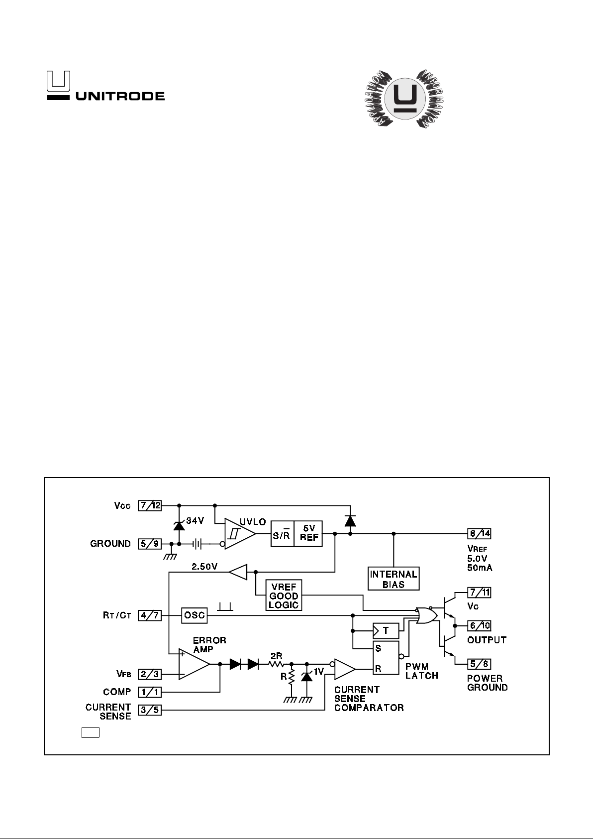
The UC1842/3/4/5 family of control ICs provides the necessary features to implement off-line or DC to DC fixed frequency cur rent mode control schemes
with a minimal external parts count . Interna l l y impleme nt ed circuits include under-voltage lockout featuring start up current less than 1mA, a precision reference trimmed for accuracy at the error amp input, logic to insure latched
operation, a PW M com parator whic h also provides current limit contr ol, and a
totem pole output stage designed to source or sink high peak current. The output stage, suitable for driving N Channel MOSFETs, is low in the off state.
Differences between members of this family are the under-voltage lockout
thresholds and maximum du ty cycle ranges. The UC1842 and UC1844 have
UVLO thresholds of 16V (on) and 10V (off), ideally suited to off-line applic ations. The correspondin g thresholds for the UC 1843 and UC1845 are 8.4V
and 7.6V. The UC1842 and UC1843 c an operate to duty cyc les approaching
100%. A range of zero t o 50 % i s o bt ain ed by t he UC 1844 and UC1845 by the
addition of an i nternal toggle flip flop which blanks the output off every other
clock cycle.
BLOCK DIAGRAM
A/B
Note 1: A = DIL-8 Pin Number. B = SO-14 Pin Number.
Note 2: Toggle flip flop used only in 1844 and 1845.
4/97
UC1842/3/4/5
UC2842/3/4/5
UC3842/3/4/5
ABSOLUTE MAXIMUM RATINGS (Note 1)
Supply Voltage (Low Impedance Source) . . . . . . . . . . . . . . . . . . . . . . . . . . . . . . . . . . 30V
Supply Voltage (ICC <30mA) . . . . . . . . . . . . . . . . . . . . . . . . . . . . . . . . . . . . . Self Limiting
Output Current . . . . . . . . . . . . . . . . . . . . . . . . . . . . . . . . . . . . . . . . . . . . . . . . . . . . . . . ±1A
Output Energy (Capacitive Load). . . . . . . . . . . . . . . . . . . . . . . . . . . . . . . . . . . . . . . . . 5µJ
Analog Inputs (Pins 2, 3) . . . . . . . . . . . . . . . . . . . . . . . . . . . . . . . . . . . . . . . -0.3V to +6.3V
Error Amp Output Sink Current . . . . . . . . . . . . . . . . . . . . . . . . . . . . . . . . . . . . . . . . . 10mA
Power Dissipation at TA ≤ 25°C (DIL-8) . . . . . . . . . . . . . . . . . . . . . . . . . . . . . . . . . . . . 1W
Power Dissipation at TA ≤ 25°C (SOIC-14). . . . . . . . . . . . . . . . . . . . . . . . . . . . . . 725mW
Storage Temperature Range . . . . . . . . . . . . . . . . . . . . . . . . . . . . . . . . . . -65°C to +150°C
Lead Temperature (Soldering, 10 Seconds) . . . . . . . . . . . . . . . . . . . . . . . . . . . . . . 300°C
Note 1: All voltages are with respect to Pin 5.
All currents are positive into the specified terminal.
Consult Packaging Section of Databook for thermal limitations and considerations
of packages.
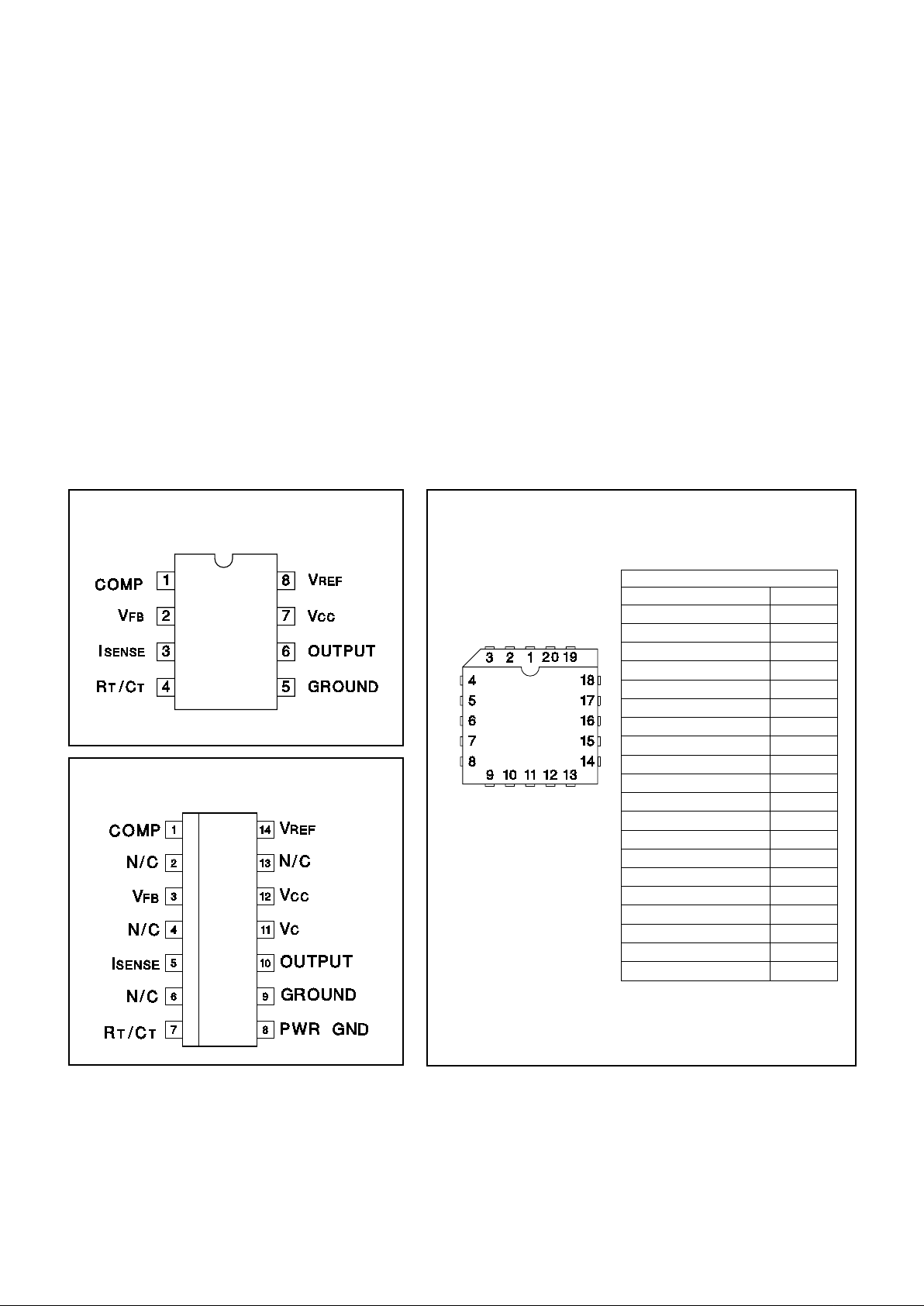
CONNECTION DIAGRAMS
DIL-8, SOIC-8 (TOP VIEW)
N or J Package, D8 Package
PLCC-20 (TOP VIEW)
Q Package
SOIC-14 (TOP VIEW)
D Package
PACKAGE PIN FUNCTION
FUNCTION PIN
N/C 1
COMP 2
N/C 3
N/C 4
V
FB
5
N/C 6
I
SENSE
7
N/C 8
N/C 9
R
T/CT
10
N/C 11
PWR GND 12
GROUND 13
N/C 14
OUTPUT 15
N/C 16
V
C
17
V
CC
18
N/C 19
V
REF
20
2
PARAMETER TEST CONDITIONS
UC1842/3/4/5
UC2842/3/4/5
UC3842/3/4/5 UNITS
MIN TYP MAX MIN TYP MAX
Reference Section
Output Voltage TJ = 25°C, IO = 1mA 4.95 5.00 5.05 4.90 5.00 5.10 V
Line Regulation 12 ≤ V
IN
≤
25V 6 20 6 20 mV
Load Regulation 1 ≤ I
0
≤ 20mA 6 25 6 25 mV
Temp. Stability (Note 2) (Note 7) 0.2 0.4 0.2 0.4 mV/°C
Total Output Variation Line, Load, Temp. (Note 2) 4.9 5.1 4.82 5.18 V
Output Noise Voltage 10Hz ≤ f ≤ 10kHz, T
J
= 25°C (Note2) 50 50
µ
V
Long Term Stability T
A
= 125°C, 1000Hrs. (Not e 2) 5 25 5 25 mV
Output Short Circuit -30 -100 -180 -30 -100 -180 mA
Oscillator Section
Initial Accuracy T
J
= 25°C (Note 6) 47 52 57 47 52 57 kHz
Voltage Stability 12 ≤ V
CC
≤ 25V 0.2 1 0.2 1 %
Temp. Stability T
MIN
≤ T
A
≤
T
MAX
(Note 2) 5 5 %
Amplitude V
PIN 4
peak to peak (Note 2) 1.7 1.7 V
Error Amp Section
Input Voltage V
PIN 1
= 2.5V 2.45 2.50 2.55 2.42 2.50 2.58 V
Input Bias Current -0.3 -1 -0. 3 -2
µ
A
A
VOL
2 ≤ V
O
≤
4V 65 90 65 90 dB
Unity Gain Bandwidth (Note 2) TJ = 25°C 0.7 1 0.7 1 MHz
PSRR 12 ≤ V
CC
≤
25V 6070 6070 dB
Output Sink Current V
PIN 2
= 2.7V, V
PIN 1
= 1.1V 2 6 2 6 mA
Output Source Current V
PIN 2
= 2.3V, V
PIN 1
= 5V -0.5 -0.8 -0.5 -0.8 mA
V
OUT
High V
PIN 2
= 2.3V, RL = 15k to ground 5 6 5 6 V
V
OUT
Low V
PIN 2
= 2.7V, RL = 15k to Pin 8 0.7 1.1 0.7 1.1 V
Current Sense Section
Gain (Notes 3 and 4) 2.85 3 3.15 2.85 3 3.15 V/V
Maximum Input Signal V
PIN 1
= 5V (Note 3) 0.9 1 1.1 0.9 1 1.1 V
PSRR 12 ≤ V
CC
≤ 25V (Note 3) (Note 2) 70 70 dB
Input Bias Current -2 -10 -2 -10
µ
A
Delay to Output V
PIN 3
= 0 to 2V (Note 2) 150 300 150 300 ns
UC1842/3/4/5
UC2842/3/4/5
UC3842/3/4/5
ELECTRICAL CHARACTERISTICS:
Unless otherwise st ated, these specific at ions apply for -55°C ≤ TA ≤ 125°C for the
UC184X; -40°C ≤ TA ≤ 85°C for the UC284X; 0°C ≤ TA ≤ 70°C for the 384X; VCC =
15V (Note 5); RT = 10k; CT =3.3nF, TA=T
J.
Note 2: These parameters, although guaranteed, are not 100% tested in production.
Note 3: Parameter measured at trip point of latch with V
PIN 2
= 0.
Note 4: Gain defined as
A
=
∆
V
PIN
1
∆
V
PIN
3
, 0 ≤
V
PIN
3
≤ 0.8
V
Note 5: Adjust V
CC
above the start thre sh old before setting at 15V.
Note 6: Output frequenc y eq ua ls osc il la t o r fr eq ue nc y fo r the UC1842 and UC1843.
Output frequency is one half oscillator frequency for the UC1844 and UC1845.
Note 7: Temperature stability, sometimes referred to as average temperature coefficient, is described by the equation:
Temp
Stability
=
V
REF
(
max
) −
V
REF
(
min
)
T
J
(
max
) −
T
J
(
min
)
V
REF
(max) and V
REF
(min) are the maximum and minimum r eference voltages measured over the appropriate
temperature range. Note that the ex tremes in voltage do not necessarily occur at the extremes in temperature.
3

PARAMETER TEST CONDITION
UC1842/3/4/5
UC2842/3/4/5
UC3842/3/4/5 UNITS
MIN TYP MAX MIN TYP MAX
Output Section
Output Low Level I
SINK
= 20mA 0.1 0.4 0.1 0.4 V
I
SINK
= 200mA 1.5 2.2 1.5 2.2 V
Output High Level I
SOURCE
= 20mA 13 13.5 13 13.5 V
I
SOURCE
= 200mA 12 13.5 12 13.5 V
Rise Time TJ = 25°C, CL = 1nF (Note 2) 50 150 50 150 ns
Fall Time T
J
= 25°C, CL = 1nF (Note 2) 50 150 50 150 ns
Under-voltage Lock ou t Secti on
Start Threshold X842/4 15 16 17 14.5 16 17.5 V
X843/5 7.8 8.4 9.0 7.8 8.4 9.0 V
Min. Operating Vol ta ge
After Turn On
X842/4 9 10 11 8.5 10 11.5 V
X843/5 7.0 7.6 8.2 7.0 7.6 8.2 V
PWM Section
Maximum Duty Cyc le X842/3 95 97 100 95 97 100 %
X844/5 46 48 50 47 48 50 %
Minimum Duty C yc le 0 0 %
Total Standby Current
Start-Up Current 0.5 1 0.5 1 mA
Operating Supply Current V
PIN 2
= V
PIN 3
= 0V 11 17 11 17 mA
V
CC
Zener Voltage I
CC
= 25mA 30 34 30 34 V
Note 2: These parameters, although guaranteed, are not 100% tested in production.
Note 3: Parameter measured at trip point of latch with V
PIN 2
= 0.
Note 4: Gain defined as:
A
=
∆
V
PIN
1
∆
V
PIN
3
; 0 ≤
V
PIN
3 ≤ 0.8
V.
Note 5: Adjust VCC above the start thre sh old before setting at 15V.
Note 6: Output frequenc y eq ua ls osc il la t o r fr eq ue nc y fo r the UC1842 and UC1843.
Output frequency is one half oscillator frequency for the UC1844 and UC1845.
UC1842/3/4/5
UC2842/3/4/5
UC3842/3/4/5
ELECTRICAL CHARACTERISTICS:
Unless otherwise st ated, these specific at ions apply for −55°C ≤ TA ≤ 125°C for the
UC184X; −40°C≤ TA ≤ 85°C for the UC284X; 0°C ≤ TA ≤ 70°C for the 384X; VCC =
15V (Note 5); RT = 10k; CT =3.3nF, TA=T
J.
ERROR AMP CONFIGURATION
Error Amp can Source or Sink up to 0.5mA
4

UC1842/3/4/5
UC2842/3/4/5
UC3842/3/4/5
UNDER-VOLTAGE LOCKOUT
CURRENT SENSE CIRCUIT
OSCILLATOR SECTION
During under-voltage lock-out, the output driver is biased to
sink minor amounts of current. Pin 6 should be shunted to
ground with a bleeder resistor to prevent activating the power
switch with extraneous leakage currents.
A small RC filter may be required to suppress switch transients
.
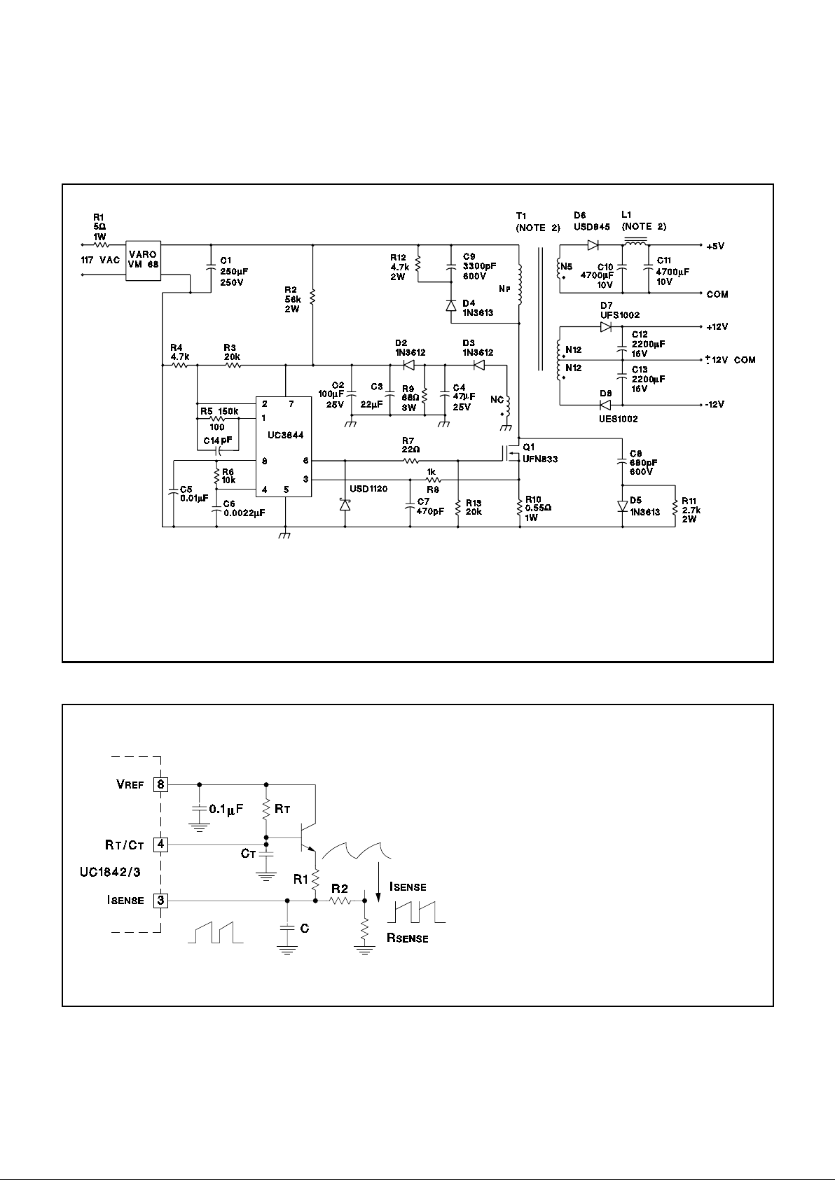
Peak Current (IS) is Determined By The Formula
I
SMAX
≈
1.0V
R
S
5

High peak currents associated with capacitive loads necessitate careful grounding techniques. Timing and bypass capacitors should be connected close to pin 5 in a single point
ground. The transistor and 5k potentiometer are used to sample the oscillator waveform and apply an adjustable ramp to
pin 3.
Shutdown of the UC1842 can be accomplished by two methods; either raise pin 3 above 1V or pull pin 1 below a voltage
two diode drops above ground. Either method causes the output of the PWM comparator to be high (refer to block diagram).
The PWM latch is reset dominant so that the output will remain
low until the next clock cycle after the shutdown condition at
pin 1 and/or 3 is removed. In one example, an externally
latched shutdown may be accomplished by adding an SCR
which will be reset by cycling V
CC
below the lower UVLO
threshold. At this point the reference turns off, allowing the
SCR to reset.
UC1842/3/4/5
UC2842/3/4/5
UC3842/3/4/5
OUTPUT SATURATION CHARACTERISTICS
ERROR AMPLIFIER OPEN-LOOP
FREQUENCY RESPONSE
OPEN-LOOP LABORATORY FIXTURE
SHUT DOWN TECHNIQUES
6
UNITRODE CORPORATION
7 CONTINENTAL BLVD. • MERRIMACK, NH 03054
TEL. (603) 424-2410 • FAX (603 ) 42 4- 34 60
UC1842/3/4/5
UC2842/3/4/5
UC3842/3/4/5
OFFLINE FLYBACK REGULATOR
SLOPE COMPENSATION
A fraction of the oscillator ramp can be resistively
summed with the current sense signal to provide slope
compensation for converters requiring duty cycles over
50%.
Note that capacitor, C forms a filter with R2 to suppress
the leading edge switch spikes.
Power Suppl y Specifications
1. Input Voltage 95VAC to 130VA
(50 Hz/60Hz)
2. Line Isolation 3750V
3. Switching Frequency 40kHz
4. Efficiency @ Full Load 70%
5. Output Voltage:
A. +5V, ±5%; 1A to 4A load
Ripple voltage: 50mV P-P Max
B. +12V, ±3%; 0.1A to 0.3A load
Ripple voltage: 100mV P-P Max
C. -12V ,±3%; 0.1A to 0.3A load
Ripple voltage: 100mV P-P Max
7

IMPORTANT NOTICE
T exas Instruments and its subsidiaries (TI) reserve the right to make changes to their products or to discontinue
any product or service without notice, and advise customers to obtain the latest version of relevant information
to verify, before placing orders, that information being relied on is current and complete. All products are sold
subject to the terms and conditions of sale supplied at the time of order acknowledgement, including those
pertaining to warranty, patent infringement, and limitation of liability.
TI warrants performance of its semiconductor products to the specifications applicable at the time of sale in
accordance with TI’s standard warranty. Testing and other quality control techniques are utilized to the extent
TI deems necessary to support this warranty. Specific testing of all parameters of each device is not necessarily
performed, except those mandated by government requirements.
CERT AIN APPLICATIONS USING SEMICONDUCTOR PRODUCTS MAY INVOLVE POTENTIAL RISKS OF
DEATH, PERSONAL INJURY, OR SEVERE PROPERTY OR ENVIRONMENTAL DAMAGE (“CRITICAL
APPLICATIONS”). TI SEMICONDUCTOR PRODUCTS ARE NOT DESIGNED, AUTHORIZED, OR
WARRANTED TO BE SUITABLE FOR USE IN LIFE-SUPPORT DEVICES OR SYSTEMS OR OTHER
CRITICAL APPLICATIONS. INCLUSION OF TI PRODUCTS IN SUCH APPLICA TIONS IS UNDERSTOOD T O
BE FULLY AT THE CUSTOMER’S RISK.
In order to minimize risks associated with the customer’s applications, adequate design and operating
safeguards must be provided by the customer to minimize inherent or procedural hazards.
TI assumes no liability for applications assistance or customer product design. TI does not warrant or represent
that any license, either express or implied, is granted under any patent right, copyright, mask work right, or other
intellectual property right of TI covering or relating to any combination, machine, or process in which such
semiconductor products or services might be or are used. TI’s publication of information regarding any third
party’s products or services does not constitute TI’s approval, warranty or endorsement thereof.
Copyright 1999, Texas Instruments Incorporated
 Loading...